EP3157067A1 - Fabrication d'une matrice de photodiodes multispectrale en cdhgte par diffusion de cadmium - Google Patents
Fabrication d'une matrice de photodiodes multispectrale en cdhgte par diffusion de cadmium Download PDFInfo
- Publication number
- EP3157067A1 EP3157067A1 EP16192974.0A EP16192974A EP3157067A1 EP 3157067 A1 EP3157067 A1 EP 3157067A1 EP 16192974 A EP16192974 A EP 16192974A EP 3157067 A1 EP3157067 A1 EP 3157067A1
- Authority
- EP
- European Patent Office
- Prior art keywords
- cadmium
- semiconductor layer
- rich
- pixel
- photodiodes
- Prior art date
- Legal status (The legal status is an assumption and is not a legal conclusion. Google has not performed a legal analysis and makes no representation as to the accuracy of the status listed.)
- Granted
Links
Images


Classifications
-
- H—ELECTRICITY
- H10—SEMICONDUCTOR DEVICES; ELECTRIC SOLID-STATE DEVICES NOT OTHERWISE PROVIDED FOR
- H10F—INORGANIC SEMICONDUCTOR DEVICES SENSITIVE TO INFRARED RADIATION, LIGHT, ELECTROMAGNETIC RADIATION OF SHORTER WAVELENGTH OR CORPUSCULAR RADIATION
- H10F39/00—Integrated devices, or assemblies of multiple devices, comprising at least one element covered by group H10F30/00, e.g. radiation detectors comprising photodiode arrays
- H10F39/011—Manufacture or treatment of image sensors covered by group H10F39/12
- H10F39/022—Manufacture or treatment of image sensors covered by group H10F39/12 of image sensors having active layers comprising only Group II-VI materials, e.g. CdS, ZnS or CdTe
-
- H—ELECTRICITY
- H10—SEMICONDUCTOR DEVICES; ELECTRIC SOLID-STATE DEVICES NOT OTHERWISE PROVIDED FOR
- H10F—INORGANIC SEMICONDUCTOR DEVICES SENSITIVE TO INFRARED RADIATION, LIGHT, ELECTROMAGNETIC RADIATION OF SHORTER WAVELENGTH OR CORPUSCULAR RADIATION
- H10F30/00—Individual radiation-sensitive semiconductor devices in which radiation controls the flow of current through the devices, e.g. photodetectors
- H10F30/20—Individual radiation-sensitive semiconductor devices in which radiation controls the flow of current through the devices, e.g. photodetectors the devices having potential barriers, e.g. phototransistors
- H10F30/21—Individual radiation-sensitive semiconductor devices in which radiation controls the flow of current through the devices, e.g. photodetectors the devices having potential barriers, e.g. phototransistors the devices being sensitive to infrared, visible or ultraviolet radiation
- H10F30/22—Individual radiation-sensitive semiconductor devices in which radiation controls the flow of current through the devices, e.g. photodetectors the devices having potential barriers, e.g. phototransistors the devices being sensitive to infrared, visible or ultraviolet radiation the devices having only one potential barrier, e.g. photodiodes
- H10F30/221—Individual radiation-sensitive semiconductor devices in which radiation controls the flow of current through the devices, e.g. photodetectors the devices having potential barriers, e.g. phototransistors the devices being sensitive to infrared, visible or ultraviolet radiation the devices having only one potential barrier, e.g. photodiodes the potential barrier being a PN homojunction
- H10F30/2212—Individual radiation-sensitive semiconductor devices in which radiation controls the flow of current through the devices, e.g. photodetectors the devices having potential barriers, e.g. phototransistors the devices being sensitive to infrared, visible or ultraviolet radiation the devices having only one potential barrier, e.g. photodiodes the potential barrier being a PN homojunction the devices comprising active layers made of only Group II-VI materials, e.g. HgCdTe infrared photodiodes
-
- H—ELECTRICITY
- H10—SEMICONDUCTOR DEVICES; ELECTRIC SOLID-STATE DEVICES NOT OTHERWISE PROVIDED FOR
- H10F—INORGANIC SEMICONDUCTOR DEVICES SENSITIVE TO INFRARED RADIATION, LIGHT, ELECTROMAGNETIC RADIATION OF SHORTER WAVELENGTH OR CORPUSCULAR RADIATION
- H10F30/00—Individual radiation-sensitive semiconductor devices in which radiation controls the flow of current through the devices, e.g. photodetectors
- H10F30/20—Individual radiation-sensitive semiconductor devices in which radiation controls the flow of current through the devices, e.g. photodetectors the devices having potential barriers, e.g. phototransistors
- H10F30/21—Individual radiation-sensitive semiconductor devices in which radiation controls the flow of current through the devices, e.g. photodetectors the devices having potential barriers, e.g. phototransistors the devices being sensitive to infrared, visible or ultraviolet radiation
- H10F30/288—Individual radiation-sensitive semiconductor devices in which radiation controls the flow of current through the devices, e.g. photodetectors the devices having potential barriers, e.g. phototransistors the devices being sensitive to infrared, visible or ultraviolet radiation the devices being sensitive to multiple wavelengths, e.g. multi-spectrum radiation detection devices
-
- H—ELECTRICITY
- H10—SEMICONDUCTOR DEVICES; ELECTRIC SOLID-STATE DEVICES NOT OTHERWISE PROVIDED FOR
- H10F—INORGANIC SEMICONDUCTOR DEVICES SENSITIVE TO INFRARED RADIATION, LIGHT, ELECTROMAGNETIC RADIATION OF SHORTER WAVELENGTH OR CORPUSCULAR RADIATION
- H10F39/00—Integrated devices, or assemblies of multiple devices, comprising at least one element covered by group H10F30/00, e.g. radiation detectors comprising photodiode arrays
- H10F39/011—Manufacture or treatment of image sensors covered by group H10F39/12
- H10F39/028—Manufacture or treatment of image sensors covered by group H10F39/12 performed after manufacture of the image sensors, e.g. annealing, gettering of impurities, short-circuit elimination or recrystallisation
-
- H—ELECTRICITY
- H10—SEMICONDUCTOR DEVICES; ELECTRIC SOLID-STATE DEVICES NOT OTHERWISE PROVIDED FOR
- H10F—INORGANIC SEMICONDUCTOR DEVICES SENSITIVE TO INFRARED RADIATION, LIGHT, ELECTROMAGNETIC RADIATION OF SHORTER WAVELENGTH OR CORPUSCULAR RADIATION
- H10F39/00—Integrated devices, or assemblies of multiple devices, comprising at least one element covered by group H10F30/00, e.g. radiation detectors comprising photodiode arrays
- H10F39/10—Integrated devices
- H10F39/12—Image sensors
- H10F39/18—Complementary metal-oxide-semiconductor [CMOS] image sensors; Photodiode array image sensors
- H10F39/184—Infrared image sensors
-
- H—ELECTRICITY
- H10—SEMICONDUCTOR DEVICES; ELECTRIC SOLID-STATE DEVICES NOT OTHERWISE PROVIDED FOR
- H10F—INORGANIC SEMICONDUCTOR DEVICES SENSITIVE TO INFRARED RADIATION, LIGHT, ELECTROMAGNETIC RADIATION OF SHORTER WAVELENGTH OR CORPUSCULAR RADIATION
- H10F39/00—Integrated devices, or assemblies of multiple devices, comprising at least one element covered by group H10F30/00, e.g. radiation detectors comprising photodiode arrays
- H10F39/80—Constructional details of image sensors
- H10F39/803—Pixels having integrated switching, control, storage or amplification elements
- H10F39/8033—Photosensitive area
-
- H—ELECTRICITY
- H10—SEMICONDUCTOR DEVICES; ELECTRIC SOLID-STATE DEVICES NOT OTHERWISE PROVIDED FOR
- H10F—INORGANIC SEMICONDUCTOR DEVICES SENSITIVE TO INFRARED RADIATION, LIGHT, ELECTROMAGNETIC RADIATION OF SHORTER WAVELENGTH OR CORPUSCULAR RADIATION
- H10F71/00—Manufacture or treatment of devices covered by this subclass
- H10F71/125—The active layers comprising only Group II-VI materials, e.g. CdS, ZnS or CdTe
- H10F71/1253—The active layers comprising only Group II-VI materials, e.g. CdS, ZnS or CdTe comprising at least three elements, e.g. HgCdTe
Definitions
- the invention relates to the field of infrared photodiodes in CdHgTe, used to detect infrared radiation, especially for applications in infrared imaging. It relates more particularly to a method of manufacturing a matrix of multi-spectral photodiodes.
- a matrix of photodiodes is said to be multi-spectral when it has a cut-off wavelength that varies in time or in space.
- the cut-off wavelength is the wavelength above which radiation is no longer detected by the photodiode.
- the cut-off wavelength of a CdHgTe photodiode depends on the cadmium concentration.
- the document EP 2 432 033 A2 describes two embodiments of a bi-spectral matrix matrix of cadmium alloy, mercury and tellurium type Cd x Hg 1-x Te.
- the matrix comprises doublets of two photodiodes mounted head to tail, separated by a barrier layer.
- a disadvantage of this embodiment is that it does not make it possible to obtain a temporal coherence of the bi-spectral detection.
- a second disadvantage is that the detection is limited to bi-spectral.
- the matrix comprises a Cd x Hg 1-x Te layer and a Cd y Hg 1-y Te layer, located one above the other and separated by a barrier layer. Trenches locally reveal the bottom layer in Cd y Hg 1-y Te, which allows for PN junctions in each of these two layers.
- a first disadvantage which is also found in the first embodiment, is that the etching of the trenches creates material defects at the etched interfaces. These defects cause a dark current and an additional noise level for the detector.
- a second disadvantage which is also found in the first embodiment, is that several growths of crystalline layers of high quality and variable composition are necessary.
- MBE molecular beam epitaxy
- EPL liquid phase epitaxy
- An object of the present invention is to provide a matrix of multi-spectral photodiodes and a related manufacturing method, not having at least one of the disadvantages of the prior art.
- a first object of the present invention is to provide a manufacturing method compatible with EPL growth techniques in addition to the EJM techniques.
- a second objective of the present invention is to propose a method of manufacturing a multi-spectral photodiode matrix of CdHgTe type which has a reduced dark current and noise level.
- a third objective of the present invention is to propose a method of manufacturing a matrix of CdHgTe type photodiodes offering multi-spectral detection, not limited to bi-spectral.
- This objective is achieved with a method for producing a matrix of multi-spectral photodiodes in a Cd x Hg 1-x Te semiconductor layer consisting of juxtaposed regions called pixels, the method comprising a step of producing a PN junction in each pixel.
- the semiconductor layer may be structured so that pixels are surmounted by respective portions of the cadmium-rich structure having different volumes (a volume being defined by a thickness and a section of said portion) and or initial concentrations, the volume may be zero.
- the concentration is said initial, to designate the concentration prior to the inter-diffusion annealing. This is a volume concentration.
- a pixel can be surmounted by a zero amount of cadmium atoms. In other words, a pixel may not be overcome by a portion of cadmium rich structure.
- the cadmium atoms of the cadmium-rich structure migrated totally or partially in the semiconductor layer below, locally modifying the cadmium concentration therein.
- the amount of cadmium atoms surmounting a pixel before annealing differs from pixel to pixel.
- the amount of cadmium atoms migrating in a pixel after annealing differs from pixel to pixel.
- not all pixels have the same cutoff wavelength.
- a matrix of multi-spectral photodiodes is thus produced, since each pixel corresponds to a photodiode.
- the method according to the invention does not impose an etching step. This eliminates the negative consequences of this etching on the electro-optical performance of the detector.
- the electro-optical performance is also improved and the manufacturing process simplified because we start from a single semiconductor layer (a single layer growth).
- the different photodiodes are not superimposed on each other, and can therefore each detect infrared radiation simultaneously.
- a multi-spectral detector with temporal coherence is thus produced.
- the invention is not limited to bi-spectral, and detectors with more than two different cutoff wavelengths can easily be made, using a plurality of possible dimensions for the portions of structure rich in cadmium.
- the process does not impose a crystalline growth of CdHgTe layer by EJM, since it implements only one CdHgTe semiconductor layer.
- a crystalline growth of HgCdTe layer by EPL is possible, with ultimately an expected gain on the manufacturing cost of the photodiode array.
- the cadmium-rich structure consists of portions, each centered on a pixel of the semiconductor layer.
- Each portion may have a form of stud, full in the center and spaced from other pads.
- each portion may have a form of stud, open in the center and spaced from other pads.
- the different portions may together form a grid having apertures each centered on a pixel.
- the cadmium-rich structure consists of portions each surmounting a pixel of the semiconductor layer, each portion being off-center relative to the corresponding pixel and several portions being formed in one piece.
- the rich cadmium structure advantageously has portions of different thicknesses.
- the cadmium-rich structure may have portions of different sections.
- the cadmium-rich structure may have portions of different initial concentrations.
- the cadmium-rich structure consists of portions each surmounting one pixel of the semiconductor layer, and comprises at least two types of portions which differ in their sections, thicknesses and / or initial concentrations.
- the cadmium-rich structure is periodic, and an elementary pattern of the periodic structure extends over a plurality of pixels of the semiconductor layer.
- the method according to the invention may comprise several cycles of the cadmium-rich material steps on the semiconductor layer and then inter-diffusion annealing.
- the semiconductor layer may have a mesa structure in which trenches separating neighboring photodiodes extend over the entire height of said semiconductor layer, the method further comprising a metallization of these trenches, making an electrical connection between the photodiodes .
- the semiconductor layer has a mesa structure in which trenches separating neighboring photodiodes do not extend over the entire height of the semiconductor layer. said semiconductor layer, so as to preserve the electrical continuity between the photodiodes.
- the invention also relates to a multi-spectral photodiode matrix obtained by a method according to the invention, in which the semiconductor layer consists of at least two types of pixels which differ in their cut-off wavelength.
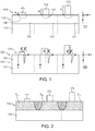
- the figure 1 illustrates a first embodiment of a method according to the invention.
- the method according to the invention is intended for the manufacture of a matrix of multi-spectral photodiodes, that is to say comprising photodiodes having different cut-off wavelengths.
- the cut-off wavelengths of two adjacent photodiodes differ by at least 1% relative to one another, preferably at least 3%.
- a matrix of planar photodiodes is produced.
- the figure 1 illustrates a matrix of photodiodes according to the invention, at different stages of its production, and in sectional views along the plane (xOz).
- the axis (Oz) is parallel to the axis of growth of the crystalline layers on a substrate 110, oriented from said crystalline layer towards the substrate.
- the axis (Ox) is orthogonal to (Oz).
- the substrate 110 is grown on the substrate 110 a single semiconductor layer 120 of Cd x Hg 1-x Te type semiconductor material.
- the substrate 110 is for example CdZnTe, or Si, or AsGa, or Ge. Growth is preferably by liquid phase epitaxy, although molecular beam epitaxy is also possible.
- composition of the Cd x Hg 1-x Te semiconductor layer is defined by the real x between 0 and 1, the terminals being excluded.
- x is considered initially constant, at least in planes orthogonal to the axis (Oz), and possibly throughout the volume of the semiconductor layer 120.
- the semiconductor layer generally has a thickness of between 100 nm and 30 ⁇ m, preferably between 100 nm and 3 ⁇ m.
- the semiconductor layer 120 consists of pixels 121. These pixels are regions of the semiconductor layer 120. These pixels are adjacent to each other. Preferably, they all have the same dimensions. On the figure 1 , the pixels 121 are delimited by vertical mixed lines. For example, they each have a rectangular parallelepiped shape.
- the figure 1 only shows three pixels.
- Each pixel 121 receives a PN junction 141.
- Each PN junction 141 separates an N or P-doped casing 140, obtained by implanting or by diffusion of doping impurities, from the remainder of this P or N-doped semiconductor layer.
- the casing is specific to the photodiode and advantageously flush with the photodiode.
- upper face of the semiconductor layer 120. The upper face of the semiconductor layer is located on the opposite side to the substrate 110.
- the semiconductor layer 120 will therefore form an optically active semiconductor layer.
- the boxes 140 are made before, after or during the implementation of the steps of the method according to the invention. To facilitate the understanding of the invention, however, they are represented in figure 1 .
- a material rich in cadmium is deposited on the semiconductor layer 120, said high cadmium material being structured to form a cadmium-rich structure 170 on the semiconductor layer 120.
- the cadmium-rich structure is deposited directly on the semiconductor layer 120, in direct physical contact with its upper face, on the opposite side to the substrate.
- the structure 170 is said to be rich in cadmium because it has a higher concentration of cadmium than that of the semiconductor layer 120.
- the initial average concentration of cadmium in the material rich in cadmium is greater than the initial average concentration of cadmium in the semiconductor layer 120.
- the cadmium-rich structure 170 is formed for example of a binary, ternary, or quaternary material, or more.
- This material advantageously comprises elements belonging to columns II and VI of the periodic table of the elements. This is for example and without limitation CdS, CdSe, CdTe, CdZnSe, CdMnSe, etc.
- the cadmium-rich structure 170 is said to be structured because it comprises through openings defining a plurality of portions of said structure.
- the cadmium-rich structure 170 consists of portions 171, 172, 173, each surmounting a pixel 121 of the semiconductor layer.
- each portion 171, 172, 173 is deposited directly on a respective pixel, in direct physical contact with its upper face, on the opposite side to the substrate.
- Each portion 171, 172, 173 covers only partially the corresponding pixel.
- Each portion 171, 172, 173 extends only above the corresponding pixel, without overflowing above a neighboring pixel.
- Each portion 171, 172, 173 has a thickness of between 10 nm and 10 ⁇ m, for example between 100 nm and 500 nm, preferably less than 300 nm.
- each pixel is surmounted by a portion of the cadmium-rich structure.
- some pixels are not overcome by any portion of the cadmium-rich structure.
- the portions 171, 172, 173 here have flat shapes, solid in the center and each centered on a pixel 121, all of which have the same initial cadmium concentration.
- the center of a pixel is defined as the center of the volume occupied by this pixel.
- These pads have here different thicknesses according to (Oz), and the same section in a plane orthogonal to the axis (Oz), parallel to the upper face of the semiconductor layer 120.
- the stud 171 has a thickness e 1 , the plot 172 a thickness e 2 , and the stud 173 a thickness e 3 , with e 1 ⁇ e 2 ⁇ e 3 .
- These pads may each have a cylinder shape of revolution. Other shapes can be used, including non-circular cylinders, square for example.
- the width of the pads, a function of the pixel pitch can for example be between 300 nm and 10 ⁇ m, for a pixel pitch of 15 ⁇ m. Each pad may cover more than 50% of the upper face of a pixel 121.
- cadmium-rich structure such as pixels being surmounted by a different quantity of cadmium atoms, for example portions of different sections or different initial concentrations. It is also possible to implement all possible combinations of thickness, section and initial concentration, such that at least one of these parameters varies from one pixel to another. More complex embodiments can also be implemented through several deposition steps of cadmium-rich material, the initial cadmium concentration and / or the shape of the pads deposited at each deposition step may vary.
- the cadmium-rich structure may have at least two types of portions that differ in their sections, thicknesses and / or initial concentrations, preferably at least two types. In a variant, all the portions forming the cadmium-rich structure are identical, and certain pixels of the semiconductor layer are not covered by any portion of the cadmium-rich structure.
- the structure rich in cadmium 170 can be achieved by a so-called lift-off photolithography technique.
- a layer of resin is deposited on the semiconductor layer 120.
- the resin is locally etched and a material rich in cadmium is deposited directly on the resin.
- the cadmium-rich material is in direct contact with the semiconductor layer 120, and forms said portions 171, 172, 173.
- the cadmium-rich material is extends on the resin.
- the resin is then removed. The cadmium-rich material is only preserved where it was in direct contact with the semiconductor layer 120.
- the thickness of the resin layer is greater than or equal to the desired thickness of the cadmium-rich structure 170. It is possible to use several resin deposition cycles, and deposition of material rich in cadmium, in particular for making plots. of different thicknesses. Materials of different initial concentrations of cadmium may be used during successive deposits.
- the cadmium-rich structure can be made by depositing a cadmium-rich material directly on the semiconductor layer 120, followed by local etching to keep the cadmium-rich material only in certain locations.
- the etching step may use a resin mask deposited on the cadmium rich material.
- the cadmium-rich material can be etched by chemical etching through through apertures in the resin mask, for example using a bromine solution. Physical engraving is also possible.
- step 102 annealing of the assembly formed by the semiconductor layer 120 and the cadmium-rich structure 170 is carried out.
- This annealing effects an inter-diffusion of the cadmium atoms, between the cadmium atoms of each portion 171, 172, 173 of the cadmium-rich structure, and the mercury atoms of the corresponding pixel.
- the annealing is preferably carried out at a temperature between 100 ° C and 500 ° C, for a period of between a few minutes and several days.
- Annealing temperature and / or duration are all the higher as the initial concentration of cadmium in the semiconductor layer 120 is important.
- the annealing temperature and duration increase with the thickness of the semiconductor layer 120.
- the annealing is carried out under saturated mercury vapor pressure.
- the annealing can be performed in one or more times.
- the annealing can also be carried out under vacuum.
- the inter-diffusion will then be slower (a mechanism limited by the displacement of mercury gaps while under saturated mercury vapor pressure, the mechanism is dominated by the diffusion of interstitials, a faster phenomenon).
- the temperature and the duration of the annealing can also take into account the technological steps used to fabricate a matrix of photodiodes according to the invention, so that the pixels of the final photodiode matrix always have different minimum concentrations of cadmium.
- L d the diffusion length of cadmium in the cadmium-rich structure 170
- t the duration of the annealing
- D the coefficient of diffusion of cadmium in the cadmium-rich structure 170, which depends on the temperature of the annealing and the concentration in cadmium. This diffusion coefficient therefore evolves during annealing in the cadmium-rich structure 170 as well as in the semiconductor layer 120, because of the inter-diffusion.
- each of the cadmium-rich pads must have a thickness less than the diffusion length of the cadmium atoms within these pads.
- the thickness of these pads can be defined as a thin layer vis-à-vis the diffusion length of cadmium.
- a semiconductor layer 120 in Cd x Hg 1-x Te with a thickness of 3 ⁇ m, with initially x 0.22, and the implementation of a P / N type technology, ie the layer semiconductor 120 is N-doped, the annealing is carried out at 300 ° C. for 40 hours, under saturated mercury vapor pressure, for cadmium-rich structures of circular dimensions 10 ⁇ m in the xOy plane and having a thickness of 100, 200 and 300nm respectively (according to Fig.1 ), for pixels with a pitch of 15 ⁇ m.
- the annealing conditions are adapted so that at the end of the annealing, the pixels do not all have the same cut-off wavelength.
- this cut-off wavelength is defined by the minimum concentration of cadmium in the pixel.
- step 102 there is shown, for each pixel and schematically, as a function of the depth z, the distribution at the end of the annealing of the cadmium atoms from the cadmium-rich structure.
- the caissons 140 are not illustrated in step 102.
- each portion 171, 172, 173 forms a finite reservoir of cadmium atoms available to diffuse into the pixel below. During annealing, the cadmium of each portion 171, 172, 173 diffuses into the corresponding pixel.
- the pixel located under the portion 171 of the cadmium-rich structure has a minimum concentration C 1 associated with a cut-off wavelength ⁇ 1
- the pixel located under the portion 172 has a minimum concentration C 2 associated a cutoff wavelength ⁇ 2
- the pixel located below the portion 173 has a minimum concentration C 3 associated with a cutoff wavelength ⁇ 3, with C 1 ⁇ C 2 ⁇ C 3.
- the concentration of cadmium in each pixel as a function of the depth may have a decreasing exponential type of form, or complementary error.
- one of the pixels of the semiconductor layer is not covered by any portion of the cadmium-rich structure, so that the annealing step does not change its minimum concentration of cadmium and the length associated cutoff waveform.
- the PN junctions are made after completion of the rich cadmium structure and annealing. It is then preferred, prior to dopant implantation, to remove what remains of the cadmium-rich structure at the end of the annealing.
- these residues of cadmium-rich structures will be removed (to maintain a better flatness of the matrix if necessary).
- the method according to the invention makes it possible to increase an average cadmium concentration at the upper face of the semiconductor layer 120, which limits the appearance of conduction channels between the photodiodes. It is therefore not necessary to delete these channels by other means. These channels of Conductions degrade the fidelity of the formed image, after reading the photodiode array by a read circuit. This increase in cadmium concentration at the upper surface of the semiconductor layer 120 also makes it possible to reduce the occurrence of pixel defects in low-frequency noise of the type 1 / f, which is beneficial for an operation of the detector. higher temperatures.
- the first embodiment of a method as illustrated in figure 1 , will advantageously be used for the manufacture of multiphase photodiodes of low pixel pitch, typically 15 ⁇ m and smaller.
- the figure 2 schematically illustrates the diffusion of cadmium the pads 171, 172, 173, in the process shown in FIG. figure 1 .
- each pad 171, 172, 173 each diffuse in a respective diffusion volume located in the corresponding pixel and may also spread on neighboring pixels.
- each diffusion volume V d1 , V d2 , V d3 includes a pixel and the edges of the adjacent pixels.
- each pad has a thickness less than the diffusion length of the cadmium in said pad (condition H ⁇ L d )
- the quantity of cadmium atoms originating from a pad of the cadmium-rich structure, and diffusing into the volume of associated diffusion increases with the dimensions of said portion. In the example illustrated here, this quantity increases with the thickness of the pads.
- the volume V d1 receives a number N 1 of cadmium atoms
- the volume V d2 V d1 receives a number N 2 > N 1 of cadmium atoms
- the volume V d3 V d2 receives a number N 3 > N 2 of cadmium atoms.
- the cadmium atoms of each pad 171, 172, 173, diffuse substantially throughout the volume of the corresponding pixel (that is to say the pixel surmounted by said pad).
- the ratio between the diffusion volume and the pixel volume may be between 1 and 1.2.
- the annealing is then adapted so that the cadmium of a portion of the cadmium-rich structure diffuses substantially throughout the volume of the pixel located below.
- the diffusion volume is not necessary, however, for the diffusion volume to be greater than or equal to the volume of a pixel so that the minimum cadmium concentration varies from pixel to pixel. Indeed, cadmium inter-diffusion can occur during the growth of the semiconductor layer 121 on a substrate comprising cadmium, which increases the concentration of cadmium throughout the bottom of the semiconductor layer 121. For this reason, the cadmium concentration in a pixel may be minimal in an area of the pixel, located at a depth z ⁇ Z0, with Z0 the thickness of the semiconductor layer 120, so not necessarily at the interface with the substrate 110.
- the diffusion volume is equal to the volume of a pixel.
- the cadmium of a portion of the rich cadmium structure diffuses throughout the volume of the pixel below without overflowing on neighboring pixels.
- the thickness of the semiconductor layer 120 may be substantially equal to half of a minimum distance between two adjacent portions of the cadmium-rich structure (taken from all the possible couples).
- the temperature and duration of the annealing are further adapted, so that the lateral diffusion length of the cadmium is equal to the depth diffusion length of the cadmium and equal to the thickness of the semiconductor layer 120.
- the lateral diffusion length of the cadmium is equal to half the minimum distance between two adjacent portions of the cadmium-rich structure, and the thickness of the semiconductor layer 120 is less than said half.
- the figure 3 schematically illustrates a matrix of photodiodes 300, obtained using the method shown in FIG. figure 1 .
- the pads 171, 172, 173 were removed after the inter-diffusion annealing step.
- the lateral dimension of the caissons 140 is advantageously of the order of the pixel pitch minus 4 to 5 ⁇ m, for example 11 ⁇ m for a pixel pitch of 15 ⁇ m. This makes it possible to improve the modulation transfer function of the pixel.
- the PN junction extends to about 1 ⁇ m below the upper surface of the semiconductor layer 120.
- the semiconductor layer 120 is covered by a passivation layer 381, open above each box to pass a metal connector 382.
- the width of a metal connector 382 is advantageously of the order of magnitude of the width of a box, or slightly less than 1 to 2 microns, for example 10 microns for a pixel pitch of 15 microns. This makes it possible to improve the quantum efficiency of the pixel while avoiding the surface inversions between the passivation and the semiconductor layer 120, specific to the presence of MIS (Metal-Insulator-Semiconductor) structure, the metallization of which is inversely polarized in the normal operating mode of the photodiode.
- MIS Metal-Insulator-Semiconductor
- the substrate can be removed before, during or after the implementation of the steps of the process according to the invention.
- matrix 300 there exists in matrix 300 at least two photodiodes each having a difference cut-off wavelength.
- the matrix 300 is therefore multi-spectral.
- the difference between their respective minimum cadmium concentrations is greater than 3% of the maximum value, or even 5%, and even 10%.
- the different types of photodiodes which differ in their cut-off wavelength, are regularly distributed in space.
- they can be distributed according to a periodic arrangement of the different types of photodiodes, with an elementary pattern comprising at least one photodiode of each type.
- An elementary pattern of the periodic structure may extend over a plurality of pixels of the semiconductor layer, of which at least one pixel is not surmounted by any portion of the cadmium rich structure.
- the photodiodes of the matrix are then divided into groups of photodiodes, respectively grouping portions, each group corresponding to an elementary pattern.
- the different types of photodiodes are distributed according to a Bayer type matrix.
- each photodiode differs in their cut-off wavelength, each photodiode providing a broadband signal which extends in the first approximation of zero (if the substrate has been removed) to the cut-off wavelength of the pixel.
- the signals of all the photodiodes of the matrix are read at the same time.
- the signals associated with photodiodes of the same group can be combined together, for example to subtract two by two, in order to have short-band signals.
- a dual-spectral detector having a small width is produced. band using the signals S 1 -S 2 and S 0 -S 1 .
- a dual-spectral detector is produced with the broadband signal S 1 and the short-wave signal S 0 -S 1 .
- a tri-spectral detector is produced at using the signals S 2 , S 1 -S 2 and S 0 -S 1 .
- a tri-color short-band detector is made using the signals S 2 -S 3 , S 1 -S 2 and S 0 -S 1 .
- the figure 4 illustrates a variant of the method and matrix of photodiodes illustrated in FIGS. Figures 1 to 3 .
- the matrix 400 illustrated in figure 4 differs from the previously disclosed embodiment in that it does not have a planar structure, but mesa.
- the mesa structure pre-exists the implementation of the method according to the invention. This type of structure offers a better quality of the modulation transfer function.
- Each photodiode has a PN junction between a box 140 having a P or N doping, and a soleplate 142 having a doping of opposite nature N or P.
- the trenches 490 separating neighboring photodiodes do not extend over the entire thickness of the semiconductor layer 120, to provide electrical continuity between the soles of the different photodiodes of the matrix. It is thus possible to polarize simultaneously all the soles of the photodiodes, with the aid of a remote electrode generally at the periphery of the matrix.
- the ratio between the depth of the trenches along the axis (Oz) and the maximum thickness of the semiconductor layer 120 along this same axis is, for example, between 0.8 and 0.9.
- This variant makes it possible very easily to obtain diffusion volumes of each portion of the cadmium-rich structure, substantially equal to the volume of a pixel of the semiconductor layer 120.
- the diffusion volume can be between 1 and 1.1 times the volume of the pixel.
- the figure 4 illustrates more particularly the matrix obtained directly after the inter-diffusion annealing.
- the semiconductor layer is covered by a passivation layer, open above each PN junction to let through a metal connector.
- the residues of the cadmium-rich structure may have been removed.
- FIGS. 5A and 5B illustrate examples of structures rich in cadmium, having portions of different thicknesses and same initial concentration of cadmium.
- FIG. 1 a perspective view of a group of photodiodes as defined above is shown.
- the pixels 121 of the semiconductor layer are delimited by dashed lines.
- the cadmium-rich structure consists of pads 570A each centered on a pixel 121, in the form of cylinders of revolution of the same diameters.
- two pixels 121 are surmounted by respective pads of thickness e 1 , and a third pixel 121 is surmounted by a pad of thickness e 2 .
- a fourth pixel is not covered by a pad of the cadmium rich structure.
- the pads are centered on the center of the PN junctions of each photodiode. They may be of greater diameter, less than or equal to the width of the PN junction.
- the cadmium-rich structures are in the form of rectangular parallelepipeds with a square base of different thicknesses, and centered on the center of the PN junctions of each photodiode.
- This embodiment in which the cadmium-rich structure consists of solid pads, is particularly suitable for matrices with a small pixel pitch.
- the Figure 5B illustrates a variant in which the pads 570B are open at the center and spaced from each other. They each have a tube shape, that is to say a cylinder of revolution open in the center, the opening being in the form of a cylinder of concentric revolution and of the same height.
- the tubes have the same internal and external diameters, and different thicknesses.
- the opening may be of smaller diameter, greater than or equal to the diameter of each PN junction, and even greater in diameter than the diameter of the space charge zones.
- the cadmium-rich structures are in the form of rectangular parallelepipeds with a square base open at the center, the opening also being in the form of rectangular parallelepipeds of the same thickness.
- This embodiment in which the cadmium-rich structure consists of open-center pads, also makes it possible to improve a modulation transfer function of the photodiode array.
- the width of these tubes will then advantageously be less than 2 .mu.m.
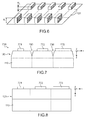
- the figure 6 illustrates another example of a cadmium-rich structure used in the process described above.
- the cadmium rich structure portions each associated with a pixel 121 of the semiconductor layer, are not centered on the associated pixel. They are also formed in one piece two by two, centered on the intersection between two neighboring pixels. They all have the same initial concentration of cadmium.
- each intersection between two neighboring studs is surmounted by a stud of height e 1 , or a stud of height e 2 , or no stud.
- the figure 6 illustrates in particular a variant according to which there are two possible geometries for the pads, and some pixels of the semiconductor layer are not covered by any portion of the cadmium-rich structure.
- the figure 7 schematically illustrates a second embodiment of a method and a matrix of photodiodes 700 according to the invention, which will be described only for its differences relative to the first embodiment.
- the semiconductor layer 120 has a mesa structure, as illustrated in FIG. figure 4 .
- the portions 771, 772, 773 of the cadmium-rich structure present this time all the same thickness according to (Oz), but different sections in a plane orthogonal to the axis (Oz) (and the same initial concentration of cadmium).
- This embodiment is particularly advantageous, since with the faded 790, the diffusion volume associated with each portion 771, 772, 773 is substantially the same, as in the case of the photodiode array 400. Indeed, these trenches limit the diffusion cadmium side in each pixel of the semiconductor layer.
- Another advantage of this embodiment is that the cadmium-rich structure portions can be deposited here in a single step, without resorting to photolithography and successive deposition as in the case described above. This simply the realization of the matrix of multi-spectral photodiodes.
- the figure 7 illustrates more particularly the matrix obtained directly after the inter-diffusion annealing.
- the semiconductor layer is covered by a passivation layer, open above each PN junction to pass a metal connector.
- the residues of the cadmium-rich structure may have been removed.
- the figure 8 schematically illustrates a variant of the method and matrix of photodiodes illustrated in FIG. figure 7 in which the matrix 800 does not have a mesa structure but a planar structure.
- the person skilled in the art may also combine the embodiments of the figures 8 and 1 to make cadmium rich structure portions having different thicknesses and sections, from one pixel to the other of the semiconductor layer.
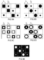
- FIGS. 9A to 9E illustrate different variants of a rich cadmium structure according to the invention, having portions of different sections.
- the Figure 9A illustrates, in top view, a series of twelve photodiodes.
- the cadmium-rich structure consists of pads (in black). Each block is a rectangular parallelepiped with a square base, centered on a photodiode and full in the center. All the pads have the same thickness. All pads do not have the same section.
- a first type of stud has a square base with a side D 1
- a second type of stud has a square base with a side D 2 ⁇ D 1 .
- the pads have a periodic arrangement, with a periodic pattern extending over a square surface of three photodiodes by three photodiodes.
- the Figure 9B does not differ from the Figure 9A that the studs have shapes of revolution cylinders of diameters D 1 or D 2 ⁇ D 1 .
- the Figure 9C does not differ from the Figure 9A that the studs all have the same external dimensions, and are crossed at the center by a through opening. (The pattern of distribution of the pads also differs very slightly.) Each pad has a section in an orthogonal plane to (Oz) in the form of a square with broad edges. All the studs have external dimensions defined by a rectangular parallelepiped with a square base of side D 1 .
- a first type of stud has a through opening in the form of a rectangular parallelepiped with a square base D 3 side.
- a second type of stud has a through opening in the form of a rectangular parallelepiped with a square base of side D 4 > D 3 .
- the Figure 9D does not differ from the Figure 9C that the studs and the through openings are each in the form of a cylinder of revolution centered on a photodiode. (The pattern of distribution of the studs corresponds to that of the Figure 9D ).
- the rich cadmium structure consists of three types of pads each associated with a photodiode.
- Each stud has external dimensions that correspond to those of the upper face of a photodiode.
- a first type of plot is full in the center.
- a second type of stud is traversed by a cylindrical through opening centered on a photodiode and first diameter.
- a third type of stud is crossed by a through opening cylindrical centered on a photodiode and second diameter. All the pads are formed in one piece so as to form a grid.
- the process may include several cadmium rich and interdiffusion annealing material deposition cycles.
- the several stages of deposition of cadmium-rich material together define a step of producing a cadmium-rich structure according to the invention.
- the several inter-diffusion annealing steps are called partial annealing. It can be considered that these partial anneals together define a single inter-diffusion annealing said fractional, after which all the pixels of the semiconductor layer do not have the same cutoff wavelength. In other words, the partial annealings are adapted so that, after these partial annealings, all the pixels of the semiconductor layer do not have the same cut-off wavelength.
- FIGS. 10A and 10B schematically illustrate a third embodiment of the method according to the invention, corresponding to this variant of the invention.
- steps are performed successively cadmium-rich material deposition and inter-diffusion annealing, said partial annealing.
- the set of partial anneals form the inter-diffusion annealing according to the invention. All deposits of cadmium-rich material form the realization of a rich cadmium structure according to the invention.
- Each deposit of cadmium-rich material may comprise the deposition of pads of the same thickness, deposited at different places on the semiconductor layer before each partial annealing.
- the residue of the studs can be removed, or preserved after annealing part.
- a stud may be superimposed, entirely or partially, on a stud that has been previously deposited and annealed.
- Plots of the same thickness may have different sections, or the same sections.
- the diffusion volume at the end of each partial annealing may be less than or equal to or the volume of the pixel.
- This embodiment is particularly advantageous with a planar semiconductor layer.
- FIGS. 10A and 10B illustrate an example of a method comprising several partial inter-scattering anneals to control the total amount of cadmium entering the pixels 121 of a planar structure.
- a first deposit of cadmium-rich material is made.
- the pad 1001 centered on the pixel 121, on the left in the figure.
- the upper face of the pixel on the right in the figure is left free.
- a first partial annealing is carried out. At the end of this first annealing, the cadmium atoms of the pad 1001 have diffused into an intermediate diffusion volume V 11 .
- a pad 1002 is added above the pixel 121 on the right in the figure.
- the pad 1002 has a much wider section than the pad 1001.
- a second partial annealing is carried out.
- the cadmium atoms of the pad 1001 have continued to diffuse in the left pixel, to finally extend into the total diffusion volume V 12 , and the cadmium atoms of pad 1002 have diffused in the total broadcast volume V 22 .
- the volumes V 12 and V 22 are substantially equal to each other, and substantially equal to the volume of a pixel of the semiconductor layer.
- the first partial annealing and the second partial annealing together form an inter-diffusion annealing as described above, here divided into two partial anneals, after which the left pixel and the right pixel on the Figures 10A and 10B do not have the same cutoff wavelength.
- This embodiment makes it possible in particular to obtain substantially equal diffusion volumes for each pixel, despite cadmium-rich pads whose section may differ greatly from one pixel to another.
- the semiconductor layer 120 is preferably very thin, for example less than the diffusion length of the minority carriers therein.
- the inter-diffusion annealing is adapted accordingly.
- a reduced thickness makes it possible to improve the FTM since the probability that a light-carrier diffuses in the neighboring pixel is reduced.
- the dark current is further reduced.
- the trenches to be engraved are shallower and therefore easier to make; thus the current of darkness will be potentially less degraded than for a deeper etching.
- a semiconductor layer of small thickness makes it possible to obtain greater variations in the cutoff wavelength within the same matrix.
- FIGS. figures 4 and 7 schematically illustrate a variant of the methods and matrices of photodiodes illustrated in FIGS. figures 4 and 7 .
- the matrix 1100 has a mesa structure, in which the trenches 1190 separating the photodiodes extend over the entire thickness of the semiconductor layer 120, up to the substrate 110.
- the matrix then has an excellent FTM.
- the cadmium diffusion volume of each cadmium rich portion of structure is limited to the pixel below. It is thus possible to use longer annealing and / or higher temperature annealing, making it possible to obtain in each pixel a homogeneous concentration of cadmium and distinct from the cadmium concentration of a neighboring pixel. Finally, greater variations in the cut-off wavelength within the same matrix can be obtained more easily.
- the figure 11A represents a sectional view of said matrix.
- the Figure 11B represents a view from above.
- metallizations 1193 are made in the trenches.
- Each metallization consists of a thin layer of electrically conductive metal covering the bottom of the trenches.
- the metallizations extend over the entirety of the inner faces of these trenches, and slightly exceed the upper face of the semiconductor layer 120, parallel to the plane (xOy).
- the metallizations together form a continuous mesh extending between the photodiodes, and connected to an electrode 1194 offset at the periphery of the matrix.
- the space charge area surrounding the PN junctions must be located away from the edges of the metallizations, to avoid a short circuit.
- An alternative to this embodiment consists in eliminating the continuity of this metallic mesh so as to relax the possible mechanical stresses induced by the deposition of a metal layer ( figure 11C ), while ensuring a low series resistance to the scale of the matrix.
- a very small rectangle is cut across the entire width of a metal line, to form an opening of the order of one micron, for example (exaggerated in figure 11C for the sake of illustration). This will be particularly advantageous for large formats of photodiode arrays.
- a last variant of this embodiment consists in eliminating metallizations in the trenches, and instead using a stronger substrate doping locally (n + or p + depending on the type of junction, obtained for example by implantation) to ensure low series resistance. at the scale of the matrix. The metallization of recovery of the substrate contact then extends only at the periphery of the matrix.
- This variant makes it possible to produce a matrix of photodiodes with very small pixel steps ( ⁇ 15 ⁇ m) for which it would be difficult to deposit a metallization in the trenches.
Landscapes
- Light Receiving Elements (AREA)
- Solid State Image Pick-Up Elements (AREA)
Abstract
- réalisation (101) d'une structure riche en cadmium (170) sur la couche semi-conductrice, structurée de façon à ce que tous les pixels (121) ne soient pas surmontés d'une même quantité d'atomes de cadmium, cette quantité pouvant être nulle ; et
- recuit d'inter-diffusion (102), réalisant la diffusion des atomes de cadmium depuis la structure riche en cadmium (170) vers la couche semi-conductrice (120).
Description
- L'invention concerne le domaine des photodiodes infrarouges en CdHgTe, utilisées pour détecter un rayonnement infrarouge, notamment pour des applications en imagerie infrarouge. Elle concerne plus particulièrement un procédé de fabrication d'une matrice de photodiodes multi-spectrale.
- Une matrice de photodiodes est dite multi-spectrale, lorsqu'elle présente une longueur d'onde de coupure qui varie dans le temps ou dans l'espace.
- La longueur d'onde de coupure est la longueur d'onde au-dessus de laquelle un rayonnement n'est plus détecté par la photodiode.
- La longueur d'onde de coupure d'une photodiode en CdHgTe dépend de la concentration en cadmium.
- Le document
EP 2 432 033 A2 , décrit deux modes de réalisation d'une matrice de photodiodes bi-spectrale en alliage de cadmium, mercure et tellure de type CdxHg1-xTe. - Dans un premier cas illustré en
figure 6 de ce document, la matrice comprend des doublets de deux photodiodes montées tête-bêche, séparées par une couche barrière. - Un inconvénient de ce mode de réalisation est qu'il ne permet pas d'obtenir une cohérence temporelle de la détection bi-spectrale.
- Un deuxième inconvénient est que la détection est limitée à du bi-spectral.
- Dans un second cas illustré en
figure 2 , la matrice comprend une couche en CdxHg1-xTe et une couche en CdyHg1-yTe, situées l'une au-dessus de l'autre et séparées par une couche barrière. Des tranchées découvrent localement la couche inférieure en CdyHg1-yTe, ce qui permet de réaliser des jonctions PN dans chacune de ces deux couches. - Un premier inconvénient, que l'on retrouve également dans le premier mode de réalisation, est que la gravure des tranchées crée des défauts de matériau aux interfaces gravées. Ces défauts sont à l'origine d'un courant d'obscurité ainsi qu'un niveau de bruit additionnel pour le détecteur.
- Un deuxième inconvénient, que l'on retrouve également dans le premier mode de réalisation, est que plusieurs croissances de couches cristallines de haute qualité et de composition variable sont nécessaires. Il est notamment nécessaire d'utiliser une croissance par épitaxie par jet moléculaire (EJM), ce type de croissance étant plus complexe qu'une croissance par épitaxie en phase liquide (EPL).
- Un objectif de la présente invention est de proposer une matrice de photodiodes multi-spectrale et un procédé de fabrication associé, ne présentant pas l'un au moins des inconvénients de l'art antérieur.
- Un premier objectif de la présente invention est de proposer un procédé de fabrication compatible avec des techniques de croissance par EPL en plus des techniques EJM.
- Un deuxième objectif de la présente invention est de proposer un procédé de fabrication d'une matrice de photodiodes multi-spectrale de type CdHgTe qui présente un courant d'obscurité et un niveau de bruit réduits.
- Un troisième objectif de la présente invention est de proposer un procédé de fabrication d'une matrice de photodiodes de type CdHgTe offrant une détection multi-spectrale, non limité à du bi-spectral.
- Cet objectif est atteint avec un procédé pour fabriquer une matrice de photodiodes multi-spectrale dans une couche semi-conductrice en CdxHg1-xTe constituée de régions juxtaposées dites pixels, le procédé comprenant une étape de réalisation d'une jonction PN dans chaque pixel.
- Le procédé selon l'invention comprend les étapes suivantes, mises en oeuvre au moins une fois :
- dépôt de matériau riche en cadmium sur la couche semi-conductrice en CdxHg1-xTe, le matériau riche en cadmium présentant une concentration en cadmium supérieure celle de la couche semi-conductrice ; puis
- recuit d'inter-diffusion, réalisant la diffusion des atomes de cadmium depuis le matériau riche en cadmium vers la couche semi-conductrice ;
l'au moins une étape de dépôt de matériau riche en cadmium formant une étape de réalisation d'une structure riche en cadmium, la structure riche en cadmium étant structurée de façon à ce que tous les pixels de la couche semi-conductrice ne soient pas surmontés d'une même quantité d'atomes de cadmium, cette quantité pouvant être nulle ; et
l'au moins un recuit d'inter-diffusion étant adapté pour qu'à l'issue de cet au moins un recuit, tous les pixels ne présentent pas la même longueur d'onde de coupure. - En d'autres termes, on peut considérer que le procédé selon l'invention comprend les étapes suivantes :
- réalisation d'une structure riche en cadmium sur la couche semi-conductrice en CdxHg1-xTe, structurée de façon à ce que tous les pixels ne soient pas surmontés d'une même quantité d'atomes de cadmium, cette quantité pouvant être nulle ; et
- recuit d'inter-diffusion, réalisant la diffusion des atomes de cadmium depuis la structure riche en cadmium vers la couche semi-conductrice, de sorte qu'à l'issue du recuit tous les pixels ne présentent pas la même longueur d'onde de coupure.
- En particulier, la couche semi-conductrice peut être structurée de façon à ce que des pixels soient surmontés de portions respectives de la structure riche en cadmium, présentant différents volumes (un volume étant défini par une épaisseur et une section de ladite portion) et/ou concentrations initiales, le volume pouvant être nul.
- La concentration est dite initiale, pour désigner la concentration préalablement au recuit d'inter-diffusion. Il s'agit d'une concentration volumique.
- Un pixel peut être surmonté d'une quantité nulle d'atomes de cadmium. En d'autres termes, un pixel peut ne pas être surmonté par une portion de structure riche en cadmium.
- A l'issue du recuit, les atomes de cadmium de la structure riche en cadmium ont migré totalement ou en partie dans la couche semi-conductrice située en dessous, modifiant localement la concentration en cadmium dans celle-ci. La quantité d'atomes de cadmium surmontant un pixel avant le recuit diffère, d'un pixel à l'autre. Par conséquent, la quantité d'atomes de cadmium ayant migré dans un pixel à l'issue du recuit diffère, d'un pixel à l'autre. Ainsi, tous les pixels ne présentent pas la même longueur d'onde de coupure. On réalise ainsi une matrice de photodiodes multi-spectrale, puisqu'à chaque pixel correspond une photodiode.
- Le procédé selon l'invention n'impose pas d'étape de gravure. On s'affranchit ainsi des conséquences négatives de cette gravure sur les performances électro-optiques du détecteur réalisé. On peut réaliser en particulier une matrice de photodiodes qui ne présente pas le courant d'obscurité et l'excès de bruit provoqués par une étape de gravure, c'est-à-dire une matrice de photodiodes qui présente un courant d'obscurité et un niveau de bruit réduits.
- Les performances électro-optiques sont également améliorées et le procédé de fabrication simplifié du fait que l'on part d'une unique couche semi-conductrice (une seule croissance de couche).
- Les différentes photodiodes ne sont pas superposées les unes sur les autres, et peuvent donc détecter chacune un rayonnement infrarouge simultanément. On réalise donc un détecteur multi-spectral à cohérence temporelle.
- L'invention n'est pas limitée à du bi-spectral, et l'on peut facilement réaliser des détecteurs à plus que deux longueurs d'onde de coupure différentes, à l'aide d'une pluralité de dimensions possibles pour les portions de structure riche en cadmium.
- Enfin, le procédé n'impose pas une croissance cristalline de couche CdHgTe par EJM, puisqu'il ne met en oeuvre qu'une seule couche semi-conductrice CdHgTe. Une croissance cristalline de couche HgCdTe par EPL est possible, avec in fine un gain attendu sur le coût de fabrication de la matrice de photodiodes.
- Selon un premier mode de réalisation, la structure riche en cadmium est constituée de portions, centrées chacune sur un pixel de la couche semi-conductrice.
- Chaque portion peut présenter une forme de plot, plein au centre et espacé des autres plots.
- En variante, chaque portion peut présenter une forme de plot, ouvert au centre et espacé des autres plots.
- Selon une autre variante, les différentes portions peuvent former ensemble une grille présentant des ouvertures centrées chacune sur un pixel.
- Selon un deuxième mode de réalisation, la structure riche en cadmium est constituée de portions surmontant chacune un pixel de la couche semi-conductrice, chaque portion étant décentrée relativement au pixel correspondant et plusieurs portions étant formées d'un seul tenant.
- La structure riche en cadmium présente avantageusement des portions de différentes épaisseurs.
- En complément ou en variante, la structure riche en cadmium peut présenter des portions de différentes sections.
- En complément ou en variante, la structure riche en cadmium peut présenter des portions de différentes concentrations initiales.
- De préférence, la structure riche en cadmium est constituée de portions surmontant chacune un pixel de la couche semi-conductrice, et comprend au moins deux types de portions qui diffèrent par leurs sections, épaisseurs et/ou concentrations initiales.
- Avantageusement, la structure riche en cadmium est périodique, et un motif élémentaire de la structure périodique s'étend au-dessus d'une pluralité de pixels de la couche semi-conductrice.
- Le procédé selon l'invention peut comprendre plusieurs cycles des étapes de matériau riche en cadmium sur la couche semi-conductrice, puis recuit d'inter-diffusion.
- La couche semi-conductrice peut présenter une structure mésa dans laquelle des tranchées séparant des photodiodes voisines s'étendent sur toute la hauteur de ladite couche semi-conductrice, le procédé comprenant en outre une métallisation de ces tranchées, réalisant une liaison électrique entre les photodiodes.
- En variante, la couche semi-conductrice présente une structure mésa dans laquelle des tranchées séparant des photodiodes voisines ne s'étendent pas sur toute la hauteur de ladite couche semi-conductrice, de façon à préserver la continuité électrique entre les photodiodes.
- L'invention concerne également une matrice de photodiodes multi-spectrale obtenue par un procédé selon l'invention, dans laquelle la couche semi-conductrice est constituée d'au moins deux types de pixels qui diffèrent par leur longueur d'onde de coupure.
- La présente invention sera mieux comprise à la lecture de la description d'exemples de réalisation donnés à titre purement indicatif et nullement limitatif, en faisant référence aux dessins annexés sur lesquels :
- la
figure 1 illustre de manière schématique un premier mode de réalisation du procédé selon l'invention ; - la
figure 2 illustre de manière schématique la diffusion du cadmium dans le procédé représenté enfigure 1 ; - la
figure 3 illustre de manière schématique une matrice de photodiodes obtenue à l'aide du procédé représenté enfigure 1 ; - la
figure 4 illustre une variante du procédé et de la matrice de photodiodes illustrés auxfigures 1 à 3 ; - les
figures 5A, 5B , et6 , illustrent deux variantes d'une structure riche en cadmium selon l'invention ; - la
figure 7 illustre de manière schématique un deuxième mode de réalisation du procédé et de la matrice de photodiodes selon l'invention ; - la
figure 8 illustre une variante du procédé et de la matrice de photodiodes illustrés à lafigure 7 ; - les
figures 9A à 9E illustrent différentes variantes d'une structure riche en cadmium selon l'invention ; et - Les
figures 10A et 10B illustrent de manière schématique un troisième mode de réalisation du procédé selon l'invention ; et - les
figures 11A, 11B et 11C illustrent de manière schématique deux variantes des procédés et matrices de photodiodes illustrés auxfigures 4 et7 . - Pour des raisons de lisibilité, les échelles ne sont pas forcément respectées sur les figures.
- La
figure 1 illustre un premier mode de réalisation d'un procédé selon l'invention. - Le procédé selon l'invention est destiné à la fabrication d'une matrice de photodiodes multi-spectrale, c'est-à-dire comprenant des photodiodes présentant différentes longueurs d'onde de coupure. Par exemple, les longueurs d'onde de coupure de deux photodiodes voisines diffèrent d'au moins 1% l'une relativement à l'autre, de préférence au moins 3%.
- Dans ce mode de réalisation, on réalise une matrice de photodiodes planaire.
- La
figure 1 illustre une matrice de photodiodes selon l'invention, à différentes étapes de sa réalisation, et selon des vues en coupe selon le plan (xOz). L'axe (Oz) est parallèle à l'axe de la croissance des couches cristallines sur un substrat 110, orienté depuis ladite couche cristalline en direction du substrat. L'axe (Ox) est orthogonal à (Oz). - Au cours d'une étape préliminaire à la mise en oeuvre de l'invention, on fait croître sur le substrat 110 une unique couche semi-conductrice 120 en matériau semi-conducteur de type CdxHg1-xTe. Le substrat 110 est par exemple en CdZnTe, ou Si, ou AsGa, ou Ge. La croissance est réalisée de préférence par épitaxie en phase liquide, bien qu'une épitaxie par jet moléculaire soit également possible.
- La composition de la couche semi-conductrice en CdxHg1-xTe est définie par x réel compris entre 0 et 1, les bornes étant exclues.
- x est considéré comme initialement constant, au moins dans des plans orthogonaux à l'axe (Oz), et possiblement dans tout le volume de la couche semi-conductrice 120.
- La couche semi-conductrice présente généralement une épaisseur comprise entre 100 nm et 30 µm, de préférence entre 100 nm et 3 µm.
- La couche semi-conductrice 120 est constituée de pixels 121. Ces pixels sont des régions de la couche semi-conductrice 120. Ces pixels sont adjacents les uns aux autres. De préférence, ils présentent tous les mêmes dimensions. Sur la
figure 1 , les pixels 121 sont délimités par des traits mixtes verticaux. Ils présentent par exemple chacun une forme de parallélépipède rectangle. - Par souci de concision, la
figure 1 n'illustre que trois pixels. - Chaque pixel 121 reçoit une jonction PN 141.
- Chaque jonction PN 141 sépare un caisson 140 dopé N ou P, obtenu par implantation ou par diffusion d'impuretés dopantes, du restant de cette couche semi-conductrice, dopée P ou N. Le caisson est spécifique à la photodiode et avantageusement affleurant sur la face supérieure de la couche semi-conductrice 120. La face supérieure de la couche semi-conductrice est située du côté opposé au substrat 110.
- La couche semi-conductrice 120 formera donc une couche semi-conductrice optiquement active.
- Les caissons 140 sont réalisés avant, après ou pendant la mise en oeuvre des étapes du procédé selon l'invention. Pour faciliter la compréhension de l'invention, ils sont cependant représentés en
figure 1 . - Dans une première étape 101 du procédé selon l'invention, on dépose un matériau riche en cadmium sur la couche semi-conductrice 120, ledit matériau riche en cadmium étant structuré pour former une structure riche en cadmium 170 sur la couche semi-conductrice 120.
- En particulier, la structure riche en cadmium est déposée directement sur la couche semi-conductrice 120, en contact physique direct avec sa face supérieure, du côté opposé au substrat.
- La structure 170 est dite riche en cadmium, car elle présente une concentration en cadmium supérieure à celle de la couche semi-conductrice 120.
- En particulier, la concentration moyenne initiale en cadmium, dans le matériau riche en cadmium, est supérieure à la concentration moyenne initiale en cadmium, dans la couche semi-conductrice 120.
- La structure riche en cadmium 170 est formée par exemple d'un matériau binaire, ternaire, ou quaternaire, voire plus. Ce matériau comprend avantageusement des éléments appartenant aux colonnes Il et VI du tableau périodique des éléments. Il s'agit par exemple et de manière non limitative de CdS, CdSe, CdTe, CdZnSe, CdMnSe, etc.
- La structure riche en cadmium 170 est dite structurée, car elle comprend des ouvertures traversantes définissant plusieurs portions de ladite structure.
- La structure riche en cadmium 170 est constituée de portions 171, 172, 173, surmontant chacune un pixel 121 de la couche semi-conductrice.
- En d'autres termes, chaque portion 171, 172, 173 est déposée directement sur un pixel respectif, en contact physique direct avec sa face supérieure, du côté opposé au substrat. Chaque portion 171, 172, 173 ne recouvre que partiellement le pixel correspondant. Chaque portion 171, 172, 173 s'étend uniquement au-dessus du pixel correspondant, sans déborder au-dessus d'un pixel voisin.
- Pour des raisons de lisibilité, sur la
figure 1 , l'épaisseur selon (Oz) de ces portions 171, 172, 173 est fortement exagérée. - Chaque portion 171, 172, 173 présente une épaisseur comprise entre 10 nm et 10 µm, par exemple entre 100 nm et 500 nm, de préférence moins de 300 nm.
- Dans l'exemple illustré en
figure 1 , chaque pixel est surmonté d'une portion de la structure riche en cadmium. En variante, certains pixels ne sont surmontés par aucune portion de la structure riche en cadmium. - Les portions 171, 172, 173 ont ici des formes de plots, pleins au centre et centrés chacun sur un pixel 121, qui présentent tous la même concentration initiale en cadmium.
- On définit le centre d'un pixel comme le centre du volume occupé par ce pixel.
- Ces plots présentent ici différentes épaisseurs selon (Oz), et la même section dans un plan orthogonal à l'axe (Oz), parallèle à la face supérieure de la couche semi-conductrice 120. Le plot 171 présente une épaisseur e1, le plot 172 une épaisseur e2, et le plot 173 une épaisseur e3, avec e1<e2<e3. Ces plots peuvent présenter chacun une forme de cylindre de révolution. D'autres formes peuvent être utilisées, notamment des cylindres à base non circulaire, carré par exemple. La largeur des plots, fonction du pas pixel, peut par exemple être comprise entre 300 nm et 10 µm, pour un pas pixel de 15µm. Chaque plot peut couvrir plus de 50% de la face supérieure d'un pixel 121.
- On présentera dans la suite d'autres exemples de réalisation des portions de la structure riche en cadmium, telles des pixels soient surmontés d'une quantité différente d'atomes de cadmium, par exemple des portions de différentes sections ou de différentes concentrations initiales. On peut également mettre en oeuvre toutes les combinaisons possibles d'épaisseur, section et concentration initiale, telle qu'au moins l'un de ces paramètres varie d'un pixel à l'autre. Des réalisations plus complexes peuvent également être mises en oeuvre grâce à plusieurs étapes de dépôt de matériau riche en cadmium, la concentration initiale en cadmium et/ou la forme des plots déposés à chaque étape de dépôt pouvant varier.
- La structure riche en cadmium peut présenter au moins deux types de portions qui diffèrent par leurs sections, épaisseurs et/ou concentrations initiales, de préférence au moins deux types. En variante, toutes les portions formant la structure riche en cadmium sont identiques, et certains pixels de la couche semi-conductrice ne sont recouverts par aucune portion de la structure riche en cadmium.
- La structure riche en cadmium 170 peut être réalisée par une technique de photolithographie dite de lift-off. Pour cela, on dépose une couche de résine sur la couche semi-conductrice 120. Ensuite, on grave localement la résine, et on dépose un matériau riche en cadmium directement sur la résine. Là où la résine est développée, le matériau riche en cadmium est en contact direct avec la couche semi-conductrice 120, et forme lesdites portions 171, 172, 173. Là où la résine n'est pas développée, le matériau riche en cadmium s'étend sur la résine. On retire ensuite la résine. Le matériau riche en cadmium n'est conservé que là où il était en contact direct avec la couche semi-conductrice 120.
- L'épaisseur de la couche de résine est supérieure ou égale à l'épaisseur souhaitée de la structure riche en cadmium 170. On peut mettre en oeuvre plusieurs cycles de dépôt de résine, et dépôt de matériau riche en cadmium, notamment pour réaliser des plots de différentes épaisseurs. Des matériaux de concentration initiale en cadmium différente pourront être utilisés lors de dépôts successifs.
- En variante, la structure riche en cadmium peut être réalisée par dépôt d'un matériau riche en cadmium directement sur la couche semi-conductrice 120, suivi d'une gravure locale pour ne conserver le matériau riche en cadmium qu'en certains emplacements. L'étape de gravure peut utiliser un masque en résine, déposé sur le matériau riche en cadmium. Le matériau riche en cadmium peut être gravé par gravure chimique à travers des ouvertures traversantes dans le masque en résine, par exemple à l'aide d'une solution de brome. Une gravure physique est également possible.
- Là encore, on peut mettre en oeuvre plusieurs cycles de dépôt de matériau riche en cadmium et gravure, le matériau riche en cadmium n'étant pas déposé toujours aux mêmes emplacements à chacun desdits cycles.
- A l'étape 102, on effectue un recuit de l'ensemble formé par la couche semi-conductrice 120 et la structure riche en cadmium 170.
- Ce recuit réalise une inter-diffusion des atomes de cadmium, entre les atomes de cadmium de chaque portion 171, 172, 173 de la structure riche en cadmium, et les atomes de mercure du pixel correspondant.
- L'homme du métier saura adapter la température et la durée du recuit pour qu'à l'issue du recuit, les pixels présentent différentes concentrations minimales en cadmium.
- Le recuit est réalisé de préférence à une température comprise entre 100°C et 500°C, pendant une durée comprise entre quelques minutes et plusieurs jours.
- On sélectionne une température et/ou une durée du recuit d'autant plus élevées que la concentration initiale en cadmium dans la couche semi-conductrice 120 est importante.
- En outre, la température et la durée du recuit augmentent avec l'épaisseur de la couche semi-conductrice 120.
- De préférence, le recuit est réalisé sous pression de vapeur saturante de mercure. Le recuit peut être réalisé en une ou plusieurs fois. Le recuit peut également être réalisé sous vide. L'inter-diffusion sera alors plus lente (mécanisme limité par le déplacement des lacunes de mercure alors que sous pression de vapeur saturante de mercure, le mécanisme est dominé par la diffusion d'interstitiels, phénomène plus rapide).
- La température et la durée du recuit peuvent également prendre en compte les étapes technologiques mises en oeuvre pour fabriquer une matrice de photodiodes selon l'invention, de sorte que les pixels de la matrice de photodiodes finale présentent toujours différentes concentrations minimales en cadmium.
- En outre, la structure riche en cadmium et le recuit sont adaptés de sorte que chaque portion de la structure riche en cadmium présente une épaisseur H, mesurée selon l'axe (Oz), telle que :

- Avec Ld la longueur de diffusion du cadmium dans la structure riche en cadmium 170, t la durée du recuit, et D le coefficient de diffusion du cadmium dans la structure riche en cadmium 170, qui dépend de la température du recuit et de la concentration en cadmium. Ce coefficient de diffusion évolue donc au cours du recuit dans la structure riche en cadmium 170 de même que dans la couche semi-conductrice 120, du fait de l'inter-diffusion.
- Cette relation traduit le fait qu'il faut que chacun des plots riches cadmium ait une épaisseur inférieure à la longueur de diffusion des atomes de cadmium au sein de ces plots. Autrement dit, l'épaisseur de ces plots peut être définie comme une couche mince vis-à-vis de la longueur de diffusion du cadmium.
- Par exemple, soit une couche semi-conductrice 120 en CdxHg1-xTe d'épaisseur 3 µm, avec initialement x=0,22, et la mise en oeuvre d'une technologique de type P/N, i.e. la couche semi-conductrice 120 est dopée N, le recuit est réalisé à 300°C pendant 40 heures, sous pression de vapeur saturante de mercure, pour des structures riches en cadmium de dimensions circulaires 10µm dans le plan xOy et d'épaisseur 100, 200 et 300nm respectivement (selon
Fig.1 ), pour des pixels au pas de 15µm. - Les conditions du recuit sont adaptées de sorte qu'à l'issue du recuit, les pixels ne présentent pas tous la même longueur d'onde de coupure.
- On peut considérer que cette longueur d'onde de coupure est définie par la concentration minimale en cadmium dans le pixel.
- Sur la
figure 1 , étape 102, on a représenté, pour chaque pixel et de façon schématique, en fonction de la profondeur z, la répartition à l'issue du recuit des atomes de cadmium provenant de la structure riche en cadmium. Afin d'alléger la figure, les caissons 140 ne sont pas illustrés à l'étape 102. - On considère qu'avant le recuit 102, les pixels présentent tous la même concentration initiale en cadmium C 0.
- De façon schématique, chaque portion 171, 172, 173 forme un réservoir fini d'atomes de cadmium disponibles pour diffuser dans le pixel situé en-dessous. Lors du recuit, le cadmium de chaque portion 171, 172, 173 diffuse dans le pixel correspondant.
- Après le recuit 102, le pixel situé sous la portion 171 de la structure riche en cadmium présente une concentration minimale C 1 associée à une longueur d'onde de coupure λ 1, le pixel situé sous la portion 172 présente une concentration minimale C 2 associée à une longueur d'onde de coupure λ 2, et le pixel situé sous la portion 173 présente une concentration minimale C 3 associée à une longueur d'onde de coupure λ 3, avec C 1 < C 2 < C 3 .
- La concentration en cadmium dans chaque pixel en fonction de la profondeur peut présenter une forme de type exponentielle décroissante, ou erreur complémentaire.
- Selon une variante non représentée, l'un des pixels de la couche semi-conductrice n'est recouvert par aucune portion de la structure riche en cadmium, de sorte que l'étape de recuit ne modifie pas sa concentration minimale en cadmium et la longueur d'onde de coupure associée.
- A l'issue du recuit, ce qui subsiste de la structure riche en cadmium peut être conservé ou retiré.
- Lorsque les jonctions PN 141 sont réalisées avant réalisation de la structure riche en cadmium et recuit, on peut conserver ce qui subsiste de la structure riche en cadmium à l'issue du recuit.
- De préférence, les jonctions PN sont réalisées après réalisation de la structure riche en cadmium et recuit. On préfère alors, avant l'implantation de dopant, retirer ce qui subsiste de la structure riche en cadmium à l'issue du recuit.
- Préférentiellement, ces résidus de structures riches en cadmium seront retirés (pour conserver une meilleure planéité de la matrice le cas échéant).
- On remarque que le procédé selon l'invention permet d'augmenter une concentration en cadmium moyenne au niveau de la face supérieure de la couche semi-conductrice 120, ce qui limite l'apparition de canaux de conduction entre les photodiodes. Il n'est donc pas nécessaire de supprimer ces canaux par d'autres moyens. Ces canaux de conductions dégradent la fidélité de l'image formée, après lecture de la matrice de photodiodes par un circuit de lecture. Cette augmentation de concentration en cadmium au niveau de la surface supérieure de la couche semi-conductrice 120 permet en outre de réduire l'apparition de défauts pixel en bruit basse fréquence de type 1/f, ce qui est bénéfique pour un fonctionnement du détecteur à de plus hautes températures.
- Le premier mode de réalisation d'un procédé, tel qu'illustrés en
figure 1 , sera avantageusement utilisé pour la fabrication de matrices de photodiodes multi-spectrales de faible pas pixel, typiquement 15µm et inférieur. - La
figure 2 illustre de manière schématique la diffusion du cadmium les plots 171, 172, 173, dans le procédé représenté enfigure 1 . - Les atomes de cadmium de chaque plot 171, 172, 173, diffusent chacun dans un volume de diffusion respectif situé dans le pixel correspondant et pouvant s'étaler également sur des pixels voisins.
- Dans l'exemple représenté en
figure 2 , chaque volume de diffusion Vd1, Vd2, Vd3 englobe un pixel et les bords des pixels adjacents. - Puisque chaque plot présente une épaisseur inférieure à la longueur de diffusion du cadmium dans ledit plot (condition H<Ld), la quantité d'atomes de cadmium provenant d'un plot de la structure riche en cadmium, et diffusant dans le volume de diffusion associé, augmente avec les dimensions de ladite portion. Dans l'exemple illustré ici, cette quantité augmente donc avec l'épaisseur des plots.
- Ainsi, le volume Vd1 reçoit un nombre N1 d'atomes de cadmium, le volume Vd2= Vd1 reçoit un nombre N2>N1 d'atomes de cadmium, et le volume Vd3= Vd2 reçoit un nombre N3>N2 d'atomes de cadmium. On obtient donc les différentes concentrations en cadmium C 1, C 2, C 3 décrites ci-dessus.
- De préférence, les atomes de cadmium de chaque plot 171, 172, 173, diffusent sensiblement dans tout le volume du pixel correspondant (c'est-à-dire le pixel surmonté par ledit plot). En particulier, ils diffusent chacun dans un volume de diffusion englobant ledit pixel correspondant, et pouvant déborder sur des pixels voisins. Le rapport entre le volume de diffusion et le volume du pixel peut être compris entre 1 et 1,2.
- En d'autres termes, le recuit est alors adapté pour que le cadmium d'une portion de la structure riche en cadmium diffuse sensiblement dans tout le volume du pixel situé en dessous.
- Il n'est cependant pas nécessaire que le volume de diffusion soit supérieur ou égal au volume d'un pixel pour que la concentration minimale en cadmium varie d'un pixel à l'autre. En effet, il peut se produire une inter-diffusion de cadmium lors de la croissance de la couche semi-conductrice 121 sur un substrat comprenant du cadmium, ce qui augmente la concentration en cadmium dans tout le fond de la couche semi-conductrice 121. Pour cette raison, la concentration en cadmium dans un pixel peut être minimale dans une zone du pixel, située à une profondeur z<Z0, avec Z0 l'épaisseur de la couche semi-conductrice 120, donc pas nécessairement à l'interface avec le substrat 110.
- Selon un mode de réalisation avantageux, le volume de diffusion est égal au volume d'un pixel. En d'autres termes, le cadmium d'une portion de la structure riche en cadmium diffuse dans tout le volume du pixel situé en dessous sans déborder sur des pixels voisins.
- Dans ce cas, l'épaisseur de la couche semi-conductrice 120 peut être sensiblement égale à la moitié d'une distance minimale entre deux portions voisines de la structure riche en cadmium (prises parmi tous les couples possibles).
- La température et la durée du recuit sont en outre adaptées, de sorte que la longueur de diffusion latérale du cadmium soit égale à la longueur de diffusion en profondeur du cadmium et égale à l'épaisseur de la couche semi-conductrice 120.
- En variante, la longueur de diffusion latérale du cadmium est égale à la moitié de la distance minimale entre deux portions voisines de la structure riche en cadmium, et l'épaisseur de la couche semi-conductrice 120 est inférieure à ladite moitié. On obtient toujours un volume de diffusion égal au volume d'un pixel, car en première approximation la diffusion du cadmium en profondeur est arrêtée à l'interface avec le substrat 110.
- La
figure 3 illustre de manière schématique une matrice de photodiodes 300, obtenue à l'aide du procédé représenté enfigure 1 . - Les plots 171, 172, 173 ont été retirés après l'étape de recuit d'inter-diffusion.
- Des caissons 140 tels que mentionnés en référence à la
figure 1 ont été réalisés après avoir retiré ces plots. - La dimension latérale des caissons 140 est avantageusement de l'ordre du pas pixel moins 4 à 5 µm, par exemple 11 µm pour un pas pixel de 15µm. Cela permet d'améliorer la fonction de transfert de modulation du pixel. La jonction PN s'étend jusqu'à environ 1 µm sous la surface supérieure de la couche semi-conductrice 120.
- La couche semi-conductrice 120 est recouverte par une couche de passivation 381, ouverte au-dessus de chaque caisson pour laisser passer un connecteur métallique 382.
- La largeur d'un connecteur métallique 382 est avantageusement de l'ordre de grandeur de la largeur d'un caisson, voire légèrement inférieure de 1 à 2 µm, par exemple 10 µm pour un pas pixel de 15 µm. Cela permet d'améliorer le rendement quantique du pixel tout en évitant les inversions de surface entre la passivation et la couche semi-conductrice 120, propre à la présence de structure MIS (Métal-Isolant-Semiconducteur) dont la métallisation est polarisée en inverse dans le mode de fonctionnement normal de la photodiode.
- Bien qu'il soit représenté à la
figure 3 , le substrat peut être retiré avant, pendant ou après la mise en oeuvre des étapes du procédé selon l'invention. - Il existe dans la matrice 300 au moins deux photodiodes présentant chacune une longueur d'onde de coupure différence. La matrice 300 est donc multi-spectrale.
- La différence entre leurs concentrations minimales en cadmium respectives est supérieure à 3% de la valeur maximale, voire 5%, et même 10%.
- De préférence, les différents types de photodiodes, qui diffèrent par leur longueur d'onde de coupure, sont répartis régulièrement dans l'espace.
- On peut notamment les répartir selon un agencement périodique des différents types de photodiodes, avec un motif élémentaire comprenant au moins une photodiode de chaque type.
- Cela correspond à une structure riche en cadmium périodique, dont le motif élémentaire s'étend au-dessus d'une pluralité de pixels de la couche semi-conductrice et présente au moins une portion de chaque type (chaque portion surmontant un unique pixel, et les portions de chaque type se distinguant les unes des autres par leur volume et/ou leur concentration initiale). Un motif élémentaire de la structure périodique peut s'étendre au-dessus d'une pluralité de pixels de la couche semi-conductrice, parmi lesquels au moins un pixel n'est surmonté d'aucune portion de la structure riche en cadmium.
- Les photodiodes de la matrice, respectivement les portions de la structure riche en cadmium, sont alors réparties en groupements de photodiodes, respectivement groupement de portions, chaque groupement correspondant à un motif élémentaire.
- Par exemple, les différents types de photodiodes, respectivement les différents types de portions de la structure riche en cadmium, sont répartis selon une matrice de type Bayer.
- Ainsi, tous les types de photodiodes ne sont pas forcément présents en même nombre, et la proportion de chaque type de photodiode permet de donner plus ou moins de poids à certaines gammes de longueur d'onde.
- Les différents types de photodiodes diffèrent par leur longueur d'onde de coupure, chaque photodiode fournissant un signal large bande qui s'étend en première approximation de zéro (si le substrat a été retiré) à la longueur d'onde de coupure du pixel.
- En fonctionnement, les signaux de toutes les photodiodes de la matrice sont lus en même temps.
- Les signaux associés à des photodiodes d'un même groupement peuvent être combinés ensemble, par exemple pour les soustraire deux à deux, afin de disposer de signaux courte bande.
- Par exemple, avec une matrice à trois types de photodiodes fournissant les signaux S0, S1 et S2, de longueurs d'onde de coupure respectives λ 0>λ 1>λ 2, on réalise un détecteur bi-spectral à faible largeur de bande à l'aide des signaux S1-S2 et S0-S1.
- En variante, avec une matrice à deux types de photodiodes fournissant les signaux S0 et S1, de longueurs d'onde de coupure respectives λ 0>λ 1, on réalise un détecteur bi-spectral avec le signal large bande S1 et le signal courte bande S0-S1.
- Selon une autre variante, avec une matrice à trois types de photodiodes fournissant les signaux S0, S1 et S2, de longueurs d'onde de coupure respectives λ 0>λ 1>λ 2, on réalise un détecteur tri-spectral à l'aide des signaux S2, S1-S2 et S0-S1.
- Selon une autre variante, avec une matrice à quatre types de photodiodes fournissant les signaux S0, S1, S2 et S3, de longueurs d'onde de coupure respectives λ 0>λ 1>λ 2>λ 3. on réalise un détecteur tricolore courtes bandes à l'aide des signaux S2-S3, S1-S2 et S0-S1.
- Le principe de ces variantes peut être étendu sans limite à des cas de détection multi-spectrale à encore plus de bandes selon les besoins du produit.
- La
figure 4 illustre une variante du procédé et de la matrice de photodiodes illustrés auxfigures 1 à 3 . - La matrice 400 illustrée en
figure 4 diffère du mode de réalisation précédemment exposé en ce qu'elle ne présente pas une structure planaire, mais mésa. - La structure mésa préexiste à la mise en oeuvre du procédé selon l'invention. Ce type de structure offre une meilleure qualité de la fonction de transfert de modulation.
- Chaque photodiode présente une jonction PN entre un caisson 140 présentant un dopage P ou N, et une semelle 142 présentant un dopage de nature opposé N ou P.
- Ici, les tranchées 490 séparant des photodiodes voisines ne s'étendent pas sur toute l'épaisseur de la couche semi-conductrice 120, afin d'offrir une continuité électrique entre les semelles des différentes photodiodes de la matrice. On peut ainsi polariser simultanément toutes les semelles des photodiodes, à l'aide d'une électrode déportée généralement en périphérie de la matrice.
- Le rapport entre la profondeur des tranchées selon l'axe (Oz) et l'épaisseur maximale de la couche semi-conductrice 120 selon ce même axe est par exemple compris entre 0,8 et 0,9.
- Cette variante permet d'obtenir très facilement des volumes de diffusion de chaque portion de la structure riche en cadmium, sensiblement égaux au volume d'un pixel de la couche semi-conductrice 120. En particulier, le volume de diffusion peut être compris entre 1 et 1,1 fois le volume du pixel.
- La
figure 4 illustre plus particulièrement la matrice obtenue directement à l'issue du recuit d'inter-diffusion. Dans le produit final, la couche semi-conductrice est recouverte par une couche de passivation, ouverte au-dessus de chaque jonction PN pour laisser passer un connecteur métallique. Les résidus de la structure riche en cadmium peuvent avoir été reti rés. - Les
figures 5A et 5B illustrent des exemples de structures riches en cadmium, présentant des portions de différentes épaisseurs et même concentration initiale en cadmium. - On a représenté en particulier une vue en perspective d'un groupement de photodiodes tel que défini ci-avant. Les pixels 121 de la couche semi-conductrice sont délimités par des traits pointillés.
- A la
figure 5A , la structure riche en cadmium est constituée de plots 570A centrés chacun sur un pixel 121, en forme de cylindres de révolution de mêmes diamètres. - Par exemple, deux pixels 121 sont surmontés de plots respectifs d'épaisseur e1, et un troisième pixel 121 est surmonté d'un plot d'épaisseur e2. Un quatrième pixel n'est pas recouvert par un plot de la structure riche en cadmium.
- Les plots sont centrés sur le centre des jonctions PN de chaque photodiode. Ils peuvent être de diamètre supérieur, inférieur ou égal à la largeur de la jonction PN.
- Selon une variante non représentée, les structures riches en cadmium sont en forme de parallélépipèdes rectangles à base carré de différentes épaisseurs, et centrés sur le centre des jonctions PN de chaque photodiode.
- Ce mode de réalisation, dans lequel la structure riche en cadmium est constituée de plots pleins, est particulièrement adapté à des matrices à faible pas de pixel.
- La
figure 5B illustre une variante dans laquelle les plots 570B sont ouverts au centre et espacés les uns des autres. Ils présentent chacun une forme de tube, c'est-à-dire de cylindre de révolution ouvert au centre, l'ouverture étant en forme de cylindre de révolution concentrique et de même hauteur. - Les tubes présentent les mêmes diamètres internes et externes, et des épaisseurs différentes.
- Ils sont centrés sur le centre des jonctions PN de chaque photodiode. L'ouverture peut être de diamètre inférieur, supérieur ou égal au diamètre de chaque jonction PN, et même de diamètre supérieur au diamètre des zones de charge d'espace.
- Selon une variante non représentée, les structures riches en cadmium sont en forme de parallélépipèdes rectangles à base carré ouverts au centre, l'ouverture étant également en forme de parallélépipèdes rectangles, de même épaisseur.
- Ce mode de réalisation, dans lequel la structure riche en cadmium est constituée de plots ouverts au centre, permet également d'améliorer une fonction de transfert de modulation de la matrice de photodiodes. La largeur de ces tubes sera alors avantageusement inférieure à 2µm.
- La
figure 6 illustre un autre exemple de structure riche en cadmium mise en oeuvre dans le procédé décrit ci-avant. Dans cet exemple, les portions de structure riche en cadmium, associées chacune à un pixel 121 de la couche semi-conductrice, ne sont pas centrées sur le pixel associées. Elles sont en outre formées d'un seul tenant deux à deux, centrées sur l'intersection entre deux pixels voisins. Elles présentent toutes la même concentration initiale en cadmium. - Le long de chaque ligne de pixels 121, chaque intersection entre deux plots voisins est surmontée par un plot de hauteur e1, ou un plot de hauteur e2, ou aucun plot.
- La
figure 6 illustre en particulier une variante selon laquelle, il y a deux géométries possibles pour les plots, et certains pixels de la couche semi-conductrice ne sont recouverts par aucune portion de la structure riche en cadmium. - De nombreuses autres formes peuvent être mises en oeuvre sans sortir du cadre de la présente invention (épaisseur et géométrie variables selon les pixels).
- La
figure 7 illustre de manière schématique un deuxième mode de réalisation d'un procédé et d'une matrice de photodiodes 700 selon l'invention, qui ne sera décrit que pour ses différences relativement au premier mode de réalisation. - Dans l'exemple illustré en
figure 7 , la couche semi-conductrice 120 présente une structure mésa, comme illustré enfigure 4 . - Les portions 771, 772, 773 de la structure riche en cadmium présentent cette fois toutes la même épaisseur selon (Oz), mais différentes sections dans un plan orthogonal à l'axe (Oz) (et la même concentration initiale en cadmium).
- Ce mode de réalisation est particulièrement avantageux, puisque grâce auxtranchées 790, le volume de diffusion associé à chaque portion 771, 772, 773 est sensiblement le même, comme dans le cas de la matrice de photodiodes 400. En effet, ces tranchées limitent la diffusion latérale du cadmium dans chaque pixel de la couche semi-conductrice. Un autre avantage de ce mode de réalisation est que les portions de structure riches en cadmium peuvent ici être déposées en une seule étape, sans avoir recours à des photolithographies et dépôts successifs comme dans le cas décrit précédemment. Ceci simplement la réalisation de la matrice de photodiodes multi-spectrale.
- La
figure 7 illustre plus particulièrement la matrice obtenue directement à l'issue du recuit d'inter-diffusion. Dans le produit final, la couche semi-conductrice est recouverte par une couche de passivation, ouverte au-dessus de chaque jonction PN pour laisser passer un connecteur métallique. Les résidus de la structure riche en cadmium peuvent avoir été reti rés. - On peut combiner les modes de réalisation des
figures 7 et4 , pour réaliser des portions de structure riche en cadmium présentant différentes épaisseurs et différentes sections, d'un pixel à l'autre de la couche semi-conductrice. - La
figure 8 illustre de manière schématique une variante du procédé et de la matrice de photodiodes illustrés à lafigure 7 , dans lequel la matrice 800 ne présente pas une structure mésa mais une structure planaire. - L'homme du métier pourra également combiner les modes de réalisation des
figures 8 et1 , pour réaliser des portions de structure riche en cadmium présentant différentes épaisseurs et différentes sections, d'un pixel à l'autre de la couche semi-conductrice. - Les
figures 9A à 9E illustrent différentes variantes d'une structure riche en cadmium selon l'invention, présentant des portions de différentes sections. - La
figure 9A illustre, en vue de dessus, une série de douze photodiodes. - La structure riche en cadmium est constituée de plots (en noir). Chaque plot est un parallélépipède rectangle à base carré, centré sur une photodiode et plein au centre. Tous les plots présentent la même épaisseur. Tous les plots ne présentent pas la même section. Un premier type de plot présente une base carré de côté D1, et un second type de plot présente une base carré de côté D2<D1. Certaines photodiodes ne sont pas surmontées par une portion de structure riche en cadmium.
- Les plots présentent un agencement périodique, avec un motif périodique s'étendant sur une surface carré de trois photodiodes par trois photodiodes.
- La
figure 9B ne diffère de lafigure 9A qu'en ce que les plots présentent des formes de cylindres de révolution de diamètres D1 ou D2<D1. - Les modes de réalisation des
figures 9A et 9B sont particulièrement avantageux pour de faibles pas de pixel de la matrice de photodiodes. - La
figure 9C ne diffère de lafigure 9A qu'en ce que les plots présentent tous les mêmes dimensions externes, et sont traversés au centre par une ouverture traversante. (Le motif de répartition des plots diffère également très légèrement.) Chaque plot présente une section dans un plan orthogonal à (Oz) en forme de carré à bords larges. Tous les plots présentent des dimensions externes définies par un parallélépipède rectangle à base carré de côté D1. Un premier type de plot présente une ouverture traversante en forme de parallélépipède rectangle à base carré de côté D3. Un second type de plot présente une ouverture traversante en forme de parallélépipède rectangle à base carré de côté D4>D3. - La
figure 9D ne diffère de lafigure 9C qu'en ce que les plots et les ouvertures traversantes sont chacun en forme de cylindre de révolution centré sur une photodiode. (Le motif de répartition des plots correspond à celui de lafigure 9D ). - Les modes de réalisation des
figures 9C et 9D permettent de réaliser une matrice de photodiodes à FTM améliorée. Les largeurs de ces tubes seront alors avantageusement inférieures à 2µm. - Dans une autre variante illustrée en
figure 9E , la structure riche en cadmium est constituée de trois types de plots associés chacun à une photodiode. Chaque plot présente des dimensions externes qui correspondent à celles de la face supérieure d'une photodiode. Un premier type de plot est plein au centre. Un deuxième type de plot est traversé par une ouverture traversante cylindrique centrée sur une photodiode et de premier diamètre. Un troisième type de plot est traversé par une ouverture traversante cylindrique centrée sur une photodiode et de second diamètre. Tous les plots sont formés d'un seul tenant de façon à constituer une grille. - De nombreuses autres formes peuvent être mises en oeuvre sans sortir du cadre de la présente invention.
- On a décrit ci-avant un procédé comprenant un unique cycle de :
- dépôt de matériau riche en cadmium, pour former une structure riche en cadmium sur la couche semi-conductrice ; et
- recuit d'inter-diffusion.
- En variante, le procédé peut comprendre plusieurs cycles de dépôt de matériau riche en cadmium et recuit d'inter-diffusion.
- Les plusieurs étapes de dépôt de matériau riche en cadmium définissent ensemble une étape de réalisation d'une structure riche en cadmium selon l'invention.
- Les plusieurs étapes de recuit d'inter-diffusion sont nommées alors recuits partiels. On peut considérer que ces recuits partiels définissent ensemble un unique recuit d'inter-diffusion dit fractionné, à l'issue duquel tous les pixels de la couche semi-conductrice ne présentent pas la même longueur d'onde de coupure. En d'autres termes, les recuits partiels sont adaptés de sorte qu'à l'issue de ces recuits partiels, tous les pixels de la couche semi-conductrice ne présentent pas la même longueur d'onde de coupure.
- Les
figures 10A et 10B illustrent de façon schématique un troisième mode de réalisation de procédé selon l'invention, correspondant à cette variante de l'invention. - Dans ce mode de réalisation, on réalise successivement des étapes de dépôt matériau riche en cadmium et recuit d'inter-diffusion, dit recuit partiel.
- L'ensemble des recuits partiels forme le recuit d'inter-diffusion selon l'invention. L'ensemble des dépôts de matériau riche en cadmium forme la réalisation d'une structure riche en cadmium selon l'invention.
- Chaque dépôt de matériau riche en cadmium peut comprendre le dépôt de plots de mêmes épaisseurs, déposées à des endroits différents sur la couche semi-conductrice avant chaque recuit partiel. Le résidu des plots peut être retiré, ou conservé après un recuit partiel. Ainsi, un plot peut être superposé, entièrement ou partiellement, sur un plot ayant été précédemment déposé et recuit. Les plots de mêmes épaisseurs peuvent présenter différentes sections, ou les mêmes sections.
- Le volume de diffusion à l'issue de chaque recuit partiel peut être inférieur ou égal ou volume du pixel.
- En fin de réalisation, selon le nombre de recuit(s) partiel(s) et de plot(s) riche(s) en cadmium qu'aura vu un pixel, sa concentration minimale en cadmium sera plus ou moins grande.
- Ce mode de réalisation est particulièrement avantageux avec une couche semi-conductrice planaire.
- Cependant, de façon avantageuse, un seul dépôt de structure riche cadmium sera effectué de façon à simplifier le procédé de fabrication.
- Les
figures 10A et 10B illustrent un exemple de procédé comprenant plusieurs recuits d'inter-diffusion partiels pour contrôler la quantité totale de cadmium rentrant dans les pixels 121 d'une structure planaire. - Au cours d'un premier cycle (
figure 10A ), on réalise un premier dépôt de matériau riche en cadmium. On dépose le plot 1001 centré le pixel 121, à gauche sur la figure. La face supérieure du pixel à droite sur la figure est laissée libre. On réalise un premier recuit partiel. A l'issue de ce premier recuit, les atomes de cadmium du plot 1001 ont diffusé dans un volume de diffusion intermédiaire V11. - Au cours d'un second cycle (
figure 10B ), on ajoute un plot 1002 au-dessus du pixel 121 à droite sur la figure. Le plot 1002 présente une section bien plus large que le plot 1001. On réalise un second recuit partiel. A l'issue de ce second recuit, les atomes de cadmium du plot 1001 ont continué à diffuser dans le pixel de gauche, pour s'étendre finalement dans le volume de diffusion total V12, et les atomes de cadmium du plot 1002 ont diffusé dans le volume de diffusion total V22. Les volumes V12 et V22 sont sensiblement égaux entre eux, et sensiblement égaux au volume d'un pixel de la couche semi-conductrice. - Le premier recuit partiel et le second recuit partiel forment ensemble un recuit d'inter-diffusion tel que décrit précédemment, fractionné ici en deux recuits partiels, à l'issue duquel le pixel de gauche et le pixel de droite sur les
figures 10A et 10B ne présentent pas la même longueur d'onde de coupure. - Ce mode de réalisation permet notamment d'obtenir des volumes de diffusion sensiblement égaux pour chaque pixel, malgré des plots riches en cadmium dont la section peut différer fortement d'un pixel à l'autre.
- En variante, on peut mettre en oeuvre des dépôts successifs de matériaux plus ou moins riches initialement en cadmium, suivi de recuit(s) d'inter-diffusion que l'homme de métier saura adapter pour obtenir des longueurs d'onde de coupure différentes d'un pixel à un pixel, ces pixels étant de préférence répartis de façon périodique à l'échelle de la matrice comme décrit précédemment.
- Quel que soit le mode de réalisation, la couche semi-conductrice 120 est de préférence très fine, par exemple inférieure à la longueur de diffusion des porteurs minoritaires dans celle-ci. Le recuit d'inter-diffusion est adapté en conséquence. Une épaisseur réduite permet d'améliorer la FTM puisque la probabilité qu'un photo-porteur diffuse dans le pixel voisin est réduite. En outre, le courant d'obscurité est encore réduit. Dans le cas particulier d'une structure mésa, les tranchées à graver sont moins profondes et donc plus faciles à réaliser; ainsi le courant d'obscurité sera potentiellement moins dégradé que pour une gravure plus profonde. Enfin, une couche semi-conductrice de faible épaisseur permet d'obtenir de plus grandes variations de la longueur d'onde de coupure au sein d'une même matrice.
- Les
figures 11A et 11B illustrent de manière schématique une variante des procédés et matrices de photodiodes illustrées auxfigures 4 et7 . - Selon cette variante, la matrice 1100 présente une structure mésa, dans laquelle les tranchées 1190 séparant les photodiodes s'étendent sur toute l'épaisseur de la couche semi-conductrice 120, jusqu'au substrat 110.
- La matrice présente alors une excellente FTM. En outre, le volume de diffusion du cadmium de chaque portion de structure riche en cadmium est limité au pixel situé en-dessous. On peut ainsi utiliser des recuits plus longs et/ou à température plus élevée, permettant d'obtenir dans chaque pixel une concentration homogène en cadmium et distinct de la concentration en cadmium d'un pixel voisin. Enfin, on peut obtenir plus facilement de plus grandes variations de la longueur d'onde de coupure au sein d'une même matrice.
- La
figure 11A représente une vue en coupe de ladite matrice. Lafigure 11B représente une vue de dessus. - Afin de rétablir un contact électrique entre les semelles de chaque photodiodes, et d'avoir une continuité électrique entre elles, on réalise des métallisations 1193 dans les tranchées. Chaque métallisation est constituée d'une fine couche de métal, électriquement conducteur, recouvrant le fond des tranchées. Dans l'exemple représenté sur les figures, les métallisations s'étendent sur l'intégralité des faces internes de ces tranchées, et dépassent légèrement sur la face supérieure de la couche semi-conductrice 120, parallèle au plan (xOy). Les métallisations forment ensemble un maillage continu s'étendant entre les photodiodes, et relié à une électrode 1194 déportée en périphérie de la matrice.
- Dans ce mode de réalisation, la zone de charge d'espace entourant les jonctions PN doit être située à distance des bords des métallisations, pour éviter un court-circuit.
- Une variante à ce mode de réalisation consiste à supprimer la continuité de ce maillage métallique de manière à relaxer les éventuelles contraintes mécaniques induites par le dépôt d'une couche métallique (
figure 11C ), tout en assurant une résistance série faible à l'échelle de la matrice. En pratique, on découpe sur toute la largeur d'une ligne métallique un tout petit rectangle, pour former une ouverture de l'ordre du micron par exemple (exagérée enfigure 11C par souci d'illustration). Ceci sera particulièrement avantageux pour les grands formats de matrices de photodiodes. - Enfin une dernière variante de ce mode de réalisation consiste s'affranchir des métallisations dans les tranchées, et à utiliser plutôt un dopage substrat plus fort localement (n+ ou p+ selon type de jonction, obtenu par exemple par implantation) pour assurer une résistance série faible à l'échelle de la matrice. La métallisation de reprise du contact substrat s'étend alors uniquement en périphérie de la matrice. Cette variante permet la réalisation de matrice de photodiodes à de très petits pas pixel (<15 µm) pour lesquels il serait difficile de déposer une métallisation dans les tranchées.
Claims (15)
- Procédé pour fabriquer une matrice (300 ; 400 ; 700 ; 800 ; 1100) de photodiodes multi-spectrale dans une couche semi-conductrice (120) en CdxHg1-xTe constituée de régions juxtaposées dites pixels (121), le procédé comprenant une étape de réalisation d'une jonction PN dans chaque pixel, caractérisé en ce qu'il comprend les étapes suivantes, mises en oeuvre au moins une fois :- dépôt (101) de matériau riche en cadmium (170 ; 1001 ; 1002) sur la couche semi-conductrice en CdxHg1-xTe, le matériau riche en cadmium (170; 1001; 1002) présentant une concentration en cadmium supérieure celle de la couche semi-conductrice (120) ; puis- recuit d'inter-diffusion (102), réalisant la diffusion des atomes de cadmium depuis le matériau riche en cadmium (170) vers la couche semi-conductrice (120) ;
l'au moins une étape de dépôt de matériau riche en cadmium (170 ; 1001 ; 1002) formant une étape de réalisation d'une structure riche en cadmium, la structure riche en cadmium étant structurée de façon à ce que tous les pixels (121) de la couche semi-conductrice ne soient pas surmontés d'une même quantité d'atomes de cadmium, cette quantité pouvant être nulle ; et
l'au moins un recuit d'inter-diffusion étant adapté pour qu'à l'issue de cet au moins un recuit, tous les pixels (121) ne présentent pas la même longueur d'onde de coupure. - Procédé selon la revendication 1, caractérisé en ce que la structure riche (170) en cadmium est constituée de portions (171 ; 172 ; 173 ; 570A ; 570B, 771 ; 772 ; 773 ; 1001 ; 1002), centrées chacune sur un pixel (121) de la couche semi-conductrice.
- Procédé selon la revendication 2, caractérisé en ce que chaque portion (171 ; 172 ; 173 ; 570A ; 771 ; 772 ; 773 ; 1001 ; 1002) présente une forme de plot, plein au centre et espacé des autres plots.
- Procédé selon la revendication 2, caractérisé en ce que chaque portion présente une forme de plot (570B), ouvert au centre et espacé des autres plots.
- Procédé selon la revendication 2, caractérisé en ce que les différentes portions forment ensemble une grille présentant des ouvertures centrées chacune sur un pixel.
- Procédé selon la revendication 1, caractérisé en ce que la structure riche en cadmium est constituée de portions surmontant chacune un pixel (121) de la couche semi-conductrice, chaque portion étant décentrée relativement au pixel correspondant et plusieurs portions étant formées d'un seul tenant.
- Procédé selon l'une quelconque des revendications 1 à 6, caractérisé en ce que la structure riche en cadmium présente des portions (171; 172 ; 173; 570A; 570B) de différentes épaisseurs.
- Procédé selon l'une quelconque des revendications 1 à 7, caractérisé en ce que la structure riche en cadmium présente des portions (771; 772 ; 773 ; 1001; 1002) de différentes sections.
- Procédé selon l'une quelconque des revendications 1 à 8, caractérisé en ce que la structure riche en cadmium présente des portions de différentes concentrations initiales.
- Procédé selon l'une quelconque des revendications 1 à 9, caractérisé en ce que la structure riche en cadmium (170) est constituée de portions surmontant chacune un pixel de la couche semi-conductrice, et comprend au moins deux types de portions (171 ; 172 ; 173 ; 570A ; 570B ; 771 ; 772 ; 773 ; 1001 ; 1002) qui diffèrent par leurs sections, épaisseurs et/ou concentrations initiales.
- Procédé selon l'une quelconque des revendications 1 à 10, caractérisé en ce que la structure riche en cadmium (170) est périodique, et en ce qu'un motif élémentaire de la structure périodique (170) s'étend au-dessus d'une pluralité de pixels (121) de la couche semi-conductrice.
- Procédé selon l'une quelconque des revendications 1 à 11, caractérisé en ce qu'il comprend plusieurs cycles des étapes de dépôt de matériau riche en cadmium sur la couche semi-conductrice, puis recuit d'inter-diffusion.
- Procédé selon l'une quelconque des revendications 1 à 12, caractérisé en ce que la couche semi-conductrice (120) présente une structure mésa dans laquelle des tranchées (1190) séparant des photodiodes voisines s'étendent sur toute la hauteur de ladite couche semi-conductrice, et en ce qu'il comprend en outre une métallisation (1190) de ces tranchées, réalisant une liaison électrique entre les photodiodes.
- Procédé selon l'une quelconque des revendications 1 à 12, caractérisé en ce que la couche semi-conductrice (120) présente une structure mésa dans laquelle des tranchées (490, 790) séparant des photodiodes voisines ne s'étendent pas sur toute la hauteur de ladite couche semi-conductrice, de façon à préserver la continuité électrique entre les photodiodes.
- Matrice de photodiodes multi-spectrale (300 ; 400 ; 700 ; 800 ; 1100) obtenue par un procédé selon l'une quelconque des revendications précédentes, dans laquelle la couche semi-conductrice est constituée d'au moins deux types de pixels qui diffèrent par leur longueur d'onde de coupure.
Applications Claiming Priority (1)
| Application Number | Priority Date | Filing Date | Title |
|---|---|---|---|
| FR1502136A FR3042310B1 (fr) | 2015-10-12 | 2015-10-12 | Fabrication d'une matrice de photodiodes multispectrale en cdhgte par diffusion de cadmium |
Publications (2)
| Publication Number | Publication Date |
|---|---|
| EP3157067A1 true EP3157067A1 (fr) | 2017-04-19 |
| EP3157067B1 EP3157067B1 (fr) | 2020-07-15 |
Family
ID=55411432
Family Applications (1)
| Application Number | Title | Priority Date | Filing Date |
|---|---|---|---|
| EP16192974.0A Active EP3157067B1 (fr) | 2015-10-12 | 2016-10-10 | Fabrication d'une matrice de photodiodes multispectrale en cdhgte par diffusion de cadmium |
Country Status (3)
| Country | Link |
|---|---|
| US (1) | US10079263B2 (fr) |
| EP (1) | EP3157067B1 (fr) |
| FR (1) | FR3042310B1 (fr) |
Cited By (2)
| Publication number | Priority date | Publication date | Assignee | Title |
|---|---|---|---|---|
| FR3113781A1 (fr) * | 2020-08-25 | 2022-03-04 | Commissariat A L'energie Atomique Et Aux Energies Alternatives | PROCÉDÉ DE FABRICATION D’UN DISPOSITIF DE PHOTODÉTECTION À FAIBLE BRUIT DANS UN SUBSTRAT EN CdHgTe. |
| US12495638B2 (en) | 2020-04-09 | 2025-12-09 | Commissariat à l'énergie atomique et aux énergies alternatives | Process for manufacturing a low-noise photodetector device in a CdHgTe substrate |
Families Citing this family (3)
| Publication number | Priority date | Publication date | Assignee | Title |
|---|---|---|---|---|
| US11508867B2 (en) * | 2020-01-28 | 2022-11-22 | Adaps Photonics Inc. | Single photon avalanche diode device |
| FR3109244B1 (fr) | 2020-04-09 | 2022-04-01 | Commissariat Energie Atomique | Dispositif de photo-détection à gradient latéral de concentration en cadmium dans la zone de charge d’espace |
| US11733408B2 (en) * | 2020-04-28 | 2023-08-22 | Redlen Technologies, Inc. | High-performance radiation detectors and methods of fabricating thereof |
Citations (9)
| Publication number | Priority date | Publication date | Assignee | Title |
|---|---|---|---|---|
| US3638026A (en) * | 1970-06-29 | 1972-01-25 | Honeywell Inc | Or photovoltaic device |
| EP0069453A1 (fr) * | 1981-06-01 | 1983-01-12 | Texas Instruments Incorporated | Procédé de fabrication d'alliages semi-conducteurs à écartement de bande désiré |
| US5861626A (en) * | 1996-04-04 | 1999-01-19 | Raytheon Ti System, Inc. | Mercury cadmium telluride infrared filters and detectors and methods of fabrication |
| US5880510A (en) * | 1988-05-11 | 1999-03-09 | Raytheon Company | Graded layer passivation of group II-VI infrared photodetectors |
| EP2432033A2 (fr) | 2010-09-16 | 2012-03-21 | Commissariat À L'Énergie Atomique Et Aux Énergies Alternatives | Détecteur bispectral multicouche à photodiodes |
| US20140319580A1 (en) * | 2011-11-28 | 2014-10-30 | Commissariat A L'energie Atomique Et Aux Ene Alt | P-n diode having a controlled heterostructure self-positioned on hgcdte, for infrared imagers |
| US20140346539A1 (en) * | 2013-05-24 | 2014-11-27 | Commissariat A L'energie Atomique Et Aux Energies Alternatives | Diode matrix device with enhanced stability |
| EP2937902A1 (fr) * | 2014-04-22 | 2015-10-28 | Commissariat à l'Énergie Atomique et aux Énergies Alternatives | MATRICE DE PHOTODIODES EN CdHgTe |
| EP2975643A1 (fr) * | 2014-07-16 | 2016-01-20 | Commissariat à l'Énergie Atomique et aux Énergies Alternatives | Matrice de photodiodes cdhgte a faible bruit |
Family Cites Families (1)
| Publication number | Priority date | Publication date | Assignee | Title |
|---|---|---|---|---|
| US5581084A (en) * | 1995-06-07 | 1996-12-03 | Santa Barbara Research Center | Simultaneous two color IR detector having common middle layer metallic contact |
-
2015
- 2015-10-12 FR FR1502136A patent/FR3042310B1/fr not_active Expired - Fee Related
-
2016
- 2016-10-10 EP EP16192974.0A patent/EP3157067B1/fr active Active
- 2016-10-10 US US15/289,577 patent/US10079263B2/en active Active
Patent Citations (9)
| Publication number | Priority date | Publication date | Assignee | Title |
|---|---|---|---|---|
| US3638026A (en) * | 1970-06-29 | 1972-01-25 | Honeywell Inc | Or photovoltaic device |
| EP0069453A1 (fr) * | 1981-06-01 | 1983-01-12 | Texas Instruments Incorporated | Procédé de fabrication d'alliages semi-conducteurs à écartement de bande désiré |
| US5880510A (en) * | 1988-05-11 | 1999-03-09 | Raytheon Company | Graded layer passivation of group II-VI infrared photodetectors |
| US5861626A (en) * | 1996-04-04 | 1999-01-19 | Raytheon Ti System, Inc. | Mercury cadmium telluride infrared filters and detectors and methods of fabrication |
| EP2432033A2 (fr) | 2010-09-16 | 2012-03-21 | Commissariat À L'Énergie Atomique Et Aux Énergies Alternatives | Détecteur bispectral multicouche à photodiodes |
| US20140319580A1 (en) * | 2011-11-28 | 2014-10-30 | Commissariat A L'energie Atomique Et Aux Ene Alt | P-n diode having a controlled heterostructure self-positioned on hgcdte, for infrared imagers |
| US20140346539A1 (en) * | 2013-05-24 | 2014-11-27 | Commissariat A L'energie Atomique Et Aux Energies Alternatives | Diode matrix device with enhanced stability |
| EP2937902A1 (fr) * | 2014-04-22 | 2015-10-28 | Commissariat à l'Énergie Atomique et aux Énergies Alternatives | MATRICE DE PHOTODIODES EN CdHgTe |
| EP2975643A1 (fr) * | 2014-07-16 | 2016-01-20 | Commissariat à l'Énergie Atomique et aux Énergies Alternatives | Matrice de photodiodes cdhgte a faible bruit |
Non-Patent Citations (2)
| Title |
|---|
| ROGALSKI A ET AL: "Third-generation infrared photodetector arrays", JOURNAL OF APPLIED PHYSICS, AMERICAN INSTITUTE OF PHYSICS, US, vol. 105, no. 9, 11 May 2009 (2009-05-11), pages 91101 - 91101, XP012125067, ISSN: 0021-8979, DOI: 10.1063/1.3099572 * |
| ROGALSKI A: "HgCdTe infrared detector material: history, status and outlook; HgCdTe infrared detector material", REPORTS ON PROGRESS IN PHYSICS, INSTITUTE OF PHYSICS PUBLISHING, BRISTOL, GB, vol. 68, no. 10, 22 August 2005 (2005-08-22), pages 2267 - 2336, XP020084623, ISSN: 0034-4885, DOI: 10.1088/0034-4885/68/10/R01 * |
Cited By (2)
| Publication number | Priority date | Publication date | Assignee | Title |
|---|---|---|---|---|
| US12495638B2 (en) | 2020-04-09 | 2025-12-09 | Commissariat à l'énergie atomique et aux énergies alternatives | Process for manufacturing a low-noise photodetector device in a CdHgTe substrate |
| FR3113781A1 (fr) * | 2020-08-25 | 2022-03-04 | Commissariat A L'energie Atomique Et Aux Energies Alternatives | PROCÉDÉ DE FABRICATION D’UN DISPOSITIF DE PHOTODÉTECTION À FAIBLE BRUIT DANS UN SUBSTRAT EN CdHgTe. |
Also Published As
| Publication number | Publication date |
|---|---|
| FR3042310B1 (fr) | 2018-10-12 |
| FR3042310A1 (fr) | 2017-04-14 |
| US10079263B2 (en) | 2018-09-18 |
| EP3157067B1 (fr) | 2020-07-15 |
| US20170104026A1 (en) | 2017-04-13 |
Similar Documents
| Publication | Publication Date | Title |
|---|---|---|
| EP3893281B1 (fr) | Dispositif a matrice de diodes photo-emettrices et/ou photo-receptrices | |
| EP0350351B1 (fr) | Photodiode et matrice de photodiodes sur matériau II-VI et leurs procédés de fabrication | |
| EP3157067B1 (fr) | Fabrication d'une matrice de photodiodes multispectrale en cdhgte par diffusion de cadmium | |
| EP2975643B1 (fr) | Matrice de photodiodes cdhgte a faible bruit | |
| EP3012876B1 (fr) | Procede de fabrication d'une photodiode a faible bruit | |
| EP2339640A1 (fr) | Photodétecteur à structure plasmon | |
| EP2937902B1 (fr) | Matrice de photodiodes en cdhgte | |
| EP2339647A1 (fr) | Photodétecteur à structure plasmon | |
| EP2432033B1 (fr) | Détecteur bispectral multicouche à photodiodes | |
| EP1756872B1 (fr) | Circuit de detection photonique a structure mesa | |
| EP2432034A2 (fr) | Détecteur bispectral multicouche à photodiodes et procédé de fabrication d'un tel détecteur | |
| FR3065580B1 (fr) | Procede de realisation d’une matrice de photodiodes a structures en mesa | |
| EP0913002B1 (fr) | Detecteur infrarouge bicolore a coherence spatio-temporelle planaire | |
| EP4133532B1 (fr) | Procédé de fabrication d'un dispositif de photodétection à faible bruit dans un substrat en cdhgte | |
| EP2950347B1 (fr) | Matrice de photodiodes mesa a ftm amelioree | |
| EP4097766B1 (fr) | Dispositif de photo-détection à gradient latéral de concentration en cadmium dans la zone de charge d'espace | |
| FR3113781A1 (fr) | PROCÉDÉ DE FABRICATION D’UN DISPOSITIF DE PHOTODÉTECTION À FAIBLE BRUIT DANS UN SUBSTRAT EN CdHgTe. | |
| FR2754107A1 (fr) | Detecteur de rayonnement photonique de grandes dimensions | |
| EP0142891B1 (fr) | Dispositif à couplage de charges sensible au rayonnement infrarouge et procédé de réalisation d'un tel dispositif | |
| WO2017032955A1 (fr) | Matrice de photodiodes a cathodes isolees | |
| WO2024141738A1 (fr) | Procédé de fabrication d'un capteur d'image | |
| FR2742581A1 (fr) | Detecteur infrarouge bicolore a coherence spatio-temporelle planaire |
Legal Events
| Date | Code | Title | Description |
|---|---|---|---|
| PUAI | Public reference made under article 153(3) epc to a published international application that has entered the european phase |
Free format text: ORIGINAL CODE: 0009012 |
|
| STAA | Information on the status of an ep patent application or granted ep patent |
Free format text: STATUS: EXAMINATION IS IN PROGRESS |
|
| 17P | Request for examination filed |
Effective date: 20161010 |
|
| AK | Designated contracting states |
Kind code of ref document: A1 Designated state(s): AL AT BE BG CH CY CZ DE DK EE ES FI FR GB GR HR HU IE IS IT LI LT LU LV MC MK MT NL NO PL PT RO RS SE SI SK SM TR |
|
| AX | Request for extension of the european patent |
Extension state: BA ME |
|
| GRAP | Despatch of communication of intention to grant a patent |
Free format text: ORIGINAL CODE: EPIDOSNIGR1 |
|
| STAA | Information on the status of an ep patent application or granted ep patent |
Free format text: STATUS: GRANT OF PATENT IS INTENDED |
|
| INTG | Intention to grant announced |
Effective date: 20200219 |
|
| GRAS | Grant fee paid |
Free format text: ORIGINAL CODE: EPIDOSNIGR3 |
|
| GRAA | (expected) grant |
Free format text: ORIGINAL CODE: 0009210 |
|
| STAA | Information on the status of an ep patent application or granted ep patent |
Free format text: STATUS: THE PATENT HAS BEEN GRANTED |
|
| AK | Designated contracting states |
Kind code of ref document: B1 Designated state(s): AL AT BE BG CH CY CZ DE DK EE ES FI FR GB GR HR HU IE IS IT LI LT LU LV MC MK MT NL NO PL PT RO RS SE SI SK SM TR |
|
| REG | Reference to a national code |
Ref country code: CH Ref legal event code: EP Ref country code: GB Ref legal event code: FG4D Free format text: NOT ENGLISH |
|
| REG | Reference to a national code |
Ref country code: IE Ref legal event code: FG4D Free format text: LANGUAGE OF EP DOCUMENT: FRENCH |
|
| REG | Reference to a national code |
Ref country code: DE Ref legal event code: R096 Ref document number: 602016039876 Country of ref document: DE |
|
| REG | Reference to a national code |
Ref country code: AT Ref legal event code: REF Ref document number: 1291961 Country of ref document: AT Kind code of ref document: T Effective date: 20200815 |
|
| REG | Reference to a national code |
Ref country code: LT Ref legal event code: MG4D |
|
| REG | Reference to a national code |
Ref country code: AT Ref legal event code: MK05 Ref document number: 1291961 Country of ref document: AT Kind code of ref document: T Effective date: 20200715 |
|
| REG | Reference to a national code |
Ref country code: NL Ref legal event code: MP Effective date: 20200715 |
|
| PG25 | Lapsed in a contracting state [announced via postgrant information from national office to epo] |
Ref country code: GR Free format text: LAPSE BECAUSE OF FAILURE TO SUBMIT A TRANSLATION OF THE DESCRIPTION OR TO PAY THE FEE WITHIN THE PRESCRIBED TIME-LIMIT Effective date: 20201016 Ref country code: ES Free format text: LAPSE BECAUSE OF FAILURE TO SUBMIT A TRANSLATION OF THE DESCRIPTION OR TO PAY THE FEE WITHIN THE PRESCRIBED TIME-LIMIT Effective date: 20200715 Ref country code: AT Free format text: LAPSE BECAUSE OF FAILURE TO SUBMIT A TRANSLATION OF THE DESCRIPTION OR TO PAY THE FEE WITHIN THE PRESCRIBED TIME-LIMIT Effective date: 20200715 Ref country code: NO Free format text: LAPSE BECAUSE OF FAILURE TO SUBMIT A TRANSLATION OF THE DESCRIPTION OR TO PAY THE FEE WITHIN THE PRESCRIBED TIME-LIMIT Effective date: 20201015 Ref country code: PT Free format text: LAPSE BECAUSE OF FAILURE TO SUBMIT A TRANSLATION OF THE DESCRIPTION OR TO PAY THE FEE WITHIN THE PRESCRIBED TIME-LIMIT Effective date: 20201116 Ref country code: BG Free format text: LAPSE BECAUSE OF FAILURE TO SUBMIT A TRANSLATION OF THE DESCRIPTION OR TO PAY THE FEE WITHIN THE PRESCRIBED TIME-LIMIT Effective date: 20201015 Ref country code: FI Free format text: LAPSE BECAUSE OF FAILURE TO SUBMIT A TRANSLATION OF THE DESCRIPTION OR TO PAY THE FEE WITHIN THE PRESCRIBED TIME-LIMIT Effective date: 20200715 Ref country code: LT Free format text: LAPSE BECAUSE OF FAILURE TO SUBMIT A TRANSLATION OF THE DESCRIPTION OR TO PAY THE FEE WITHIN THE PRESCRIBED TIME-LIMIT Effective date: 20200715 Ref country code: SE Free format text: LAPSE BECAUSE OF FAILURE TO SUBMIT A TRANSLATION OF THE DESCRIPTION OR TO PAY THE FEE WITHIN THE PRESCRIBED TIME-LIMIT Effective date: 20200715 Ref country code: HR Free format text: LAPSE BECAUSE OF FAILURE TO SUBMIT A TRANSLATION OF THE DESCRIPTION OR TO PAY THE FEE WITHIN THE PRESCRIBED TIME-LIMIT Effective date: 20200715 |
|
| PG25 | Lapsed in a contracting state [announced via postgrant information from national office to epo] |
Ref country code: LV Free format text: LAPSE BECAUSE OF FAILURE TO SUBMIT A TRANSLATION OF THE DESCRIPTION OR TO PAY THE FEE WITHIN THE PRESCRIBED TIME-LIMIT Effective date: 20200715 Ref country code: PL Free format text: LAPSE BECAUSE OF FAILURE TO SUBMIT A TRANSLATION OF THE DESCRIPTION OR TO PAY THE FEE WITHIN THE PRESCRIBED TIME-LIMIT Effective date: 20200715 Ref country code: RS Free format text: LAPSE BECAUSE OF FAILURE TO SUBMIT A TRANSLATION OF THE DESCRIPTION OR TO PAY THE FEE WITHIN THE PRESCRIBED TIME-LIMIT Effective date: 20200715 Ref country code: IS Free format text: LAPSE BECAUSE OF FAILURE TO SUBMIT A TRANSLATION OF THE DESCRIPTION OR TO PAY THE FEE WITHIN THE PRESCRIBED TIME-LIMIT Effective date: 20201115 |
|
| PG25 | Lapsed in a contracting state [announced via postgrant information from national office to epo] |
Ref country code: NL Free format text: LAPSE BECAUSE OF FAILURE TO SUBMIT A TRANSLATION OF THE DESCRIPTION OR TO PAY THE FEE WITHIN THE PRESCRIBED TIME-LIMIT Effective date: 20200715 |
|
| REG | Reference to a national code |
Ref country code: DE Ref legal event code: R097 Ref document number: 602016039876 Country of ref document: DE |
|
| PG25 | Lapsed in a contracting state [announced via postgrant information from national office to epo] |
Ref country code: IT Free format text: LAPSE BECAUSE OF FAILURE TO SUBMIT A TRANSLATION OF THE DESCRIPTION OR TO PAY THE FEE WITHIN THE PRESCRIBED TIME-LIMIT Effective date: 20200715 Ref country code: EE Free format text: LAPSE BECAUSE OF FAILURE TO SUBMIT A TRANSLATION OF THE DESCRIPTION OR TO PAY THE FEE WITHIN THE PRESCRIBED TIME-LIMIT Effective date: 20200715 Ref country code: CZ Free format text: LAPSE BECAUSE OF FAILURE TO SUBMIT A TRANSLATION OF THE DESCRIPTION OR TO PAY THE FEE WITHIN THE PRESCRIBED TIME-LIMIT Effective date: 20200715 Ref country code: DK Free format text: LAPSE BECAUSE OF FAILURE TO SUBMIT A TRANSLATION OF THE DESCRIPTION OR TO PAY THE FEE WITHIN THE PRESCRIBED TIME-LIMIT Effective date: 20200715 Ref country code: SM Free format text: LAPSE BECAUSE OF FAILURE TO SUBMIT A TRANSLATION OF THE DESCRIPTION OR TO PAY THE FEE WITHIN THE PRESCRIBED TIME-LIMIT Effective date: 20200715 Ref country code: RO Free format text: LAPSE BECAUSE OF FAILURE TO SUBMIT A TRANSLATION OF THE DESCRIPTION OR TO PAY THE FEE WITHIN THE PRESCRIBED TIME-LIMIT Effective date: 20200715 |
|
| PLBE | No opposition filed within time limit |
Free format text: ORIGINAL CODE: 0009261 |
|
| STAA | Information on the status of an ep patent application or granted ep patent |
Free format text: STATUS: NO OPPOSITION FILED WITHIN TIME LIMIT |
|
| PG25 | Lapsed in a contracting state [announced via postgrant information from national office to epo] |
Ref country code: AL Free format text: LAPSE BECAUSE OF FAILURE TO SUBMIT A TRANSLATION OF THE DESCRIPTION OR TO PAY THE FEE WITHIN THE PRESCRIBED TIME-LIMIT Effective date: 20200715 |
|
| REG | Reference to a national code |
Ref country code: CH Ref legal event code: PL |
|
| 26N | No opposition filed |
Effective date: 20210416 |
|
| PG25 | Lapsed in a contracting state [announced via postgrant information from national office to epo] |
Ref country code: LU Free format text: LAPSE BECAUSE OF NON-PAYMENT OF DUE FEES Effective date: 20201010 Ref country code: MC Free format text: LAPSE BECAUSE OF FAILURE TO SUBMIT A TRANSLATION OF THE DESCRIPTION OR TO PAY THE FEE WITHIN THE PRESCRIBED TIME-LIMIT Effective date: 20200715 Ref country code: SK Free format text: LAPSE BECAUSE OF FAILURE TO SUBMIT A TRANSLATION OF THE DESCRIPTION OR TO PAY THE FEE WITHIN THE PRESCRIBED TIME-LIMIT Effective date: 20200715 |
|
| REG | Reference to a national code |
Ref country code: BE Ref legal event code: MM Effective date: 20201031 |
|
| PG25 | Lapsed in a contracting state [announced via postgrant information from national office to epo] |
Ref country code: BE Free format text: LAPSE BECAUSE OF NON-PAYMENT OF DUE FEES Effective date: 20201031 Ref country code: CH Free format text: LAPSE BECAUSE OF NON-PAYMENT OF DUE FEES Effective date: 20201031 Ref country code: SI Free format text: LAPSE BECAUSE OF FAILURE TO SUBMIT A TRANSLATION OF THE DESCRIPTION OR TO PAY THE FEE WITHIN THE PRESCRIBED TIME-LIMIT Effective date: 20200715 Ref country code: LI Free format text: LAPSE BECAUSE OF NON-PAYMENT OF DUE FEES Effective date: 20201031 |
|
| PG25 | Lapsed in a contracting state [announced via postgrant information from national office to epo] |
Ref country code: IE Free format text: LAPSE BECAUSE OF NON-PAYMENT OF DUE FEES Effective date: 20201010 |
|
| PG25 | Lapsed in a contracting state [announced via postgrant information from national office to epo] |
Ref country code: TR Free format text: LAPSE BECAUSE OF FAILURE TO SUBMIT A TRANSLATION OF THE DESCRIPTION OR TO PAY THE FEE WITHIN THE PRESCRIBED TIME-LIMIT Effective date: 20200715 Ref country code: MT Free format text: LAPSE BECAUSE OF FAILURE TO SUBMIT A TRANSLATION OF THE DESCRIPTION OR TO PAY THE FEE WITHIN THE PRESCRIBED TIME-LIMIT Effective date: 20200715 Ref country code: CY Free format text: LAPSE BECAUSE OF FAILURE TO SUBMIT A TRANSLATION OF THE DESCRIPTION OR TO PAY THE FEE WITHIN THE PRESCRIBED TIME-LIMIT Effective date: 20200715 |
|
| PG25 | Lapsed in a contracting state [announced via postgrant information from national office to epo] |
Ref country code: MK Free format text: LAPSE BECAUSE OF FAILURE TO SUBMIT A TRANSLATION OF THE DESCRIPTION OR TO PAY THE FEE WITHIN THE PRESCRIBED TIME-LIMIT Effective date: 20200715 |
|
| REG | Reference to a national code |
Ref country code: DE Ref legal event code: R079 Ref document number: 602016039876 Country of ref document: DE Free format text: PREVIOUS MAIN CLASS: H01L0031101000 Ipc: H10F0030210000 |
|
| PGFP | Annual fee paid to national office [announced via postgrant information from national office to epo] |
Ref country code: DE Payment date: 20251020 Year of fee payment: 10 |
|
| PGFP | Annual fee paid to national office [announced via postgrant information from national office to epo] |
Ref country code: GB Payment date: 20251029 Year of fee payment: 10 |
|
| PGFP | Annual fee paid to national office [announced via postgrant information from national office to epo] |
Ref country code: FR Payment date: 20251024 Year of fee payment: 10 |