EP3157054A1 - Apparatus for regulating the temperature of an electronic device in a housing, a method and an assembly - Google Patents
Apparatus for regulating the temperature of an electronic device in a housing, a method and an assembly Download PDFInfo
- Publication number
- EP3157054A1 EP3157054A1 EP15306616.2A EP15306616A EP3157054A1 EP 3157054 A1 EP3157054 A1 EP 3157054A1 EP 15306616 A EP15306616 A EP 15306616A EP 3157054 A1 EP3157054 A1 EP 3157054A1
- Authority
- EP
- European Patent Office
- Prior art keywords
- electronic package
- heat sink
- clip
- temperature
- bimetallic
- Prior art date
- Legal status (The legal status is an assumption and is not a legal conclusion. Google has not performed a legal analysis and makes no representation as to the accuracy of the status listed.)
- Granted
Links
Images



Classifications
-
- H—ELECTRICITY
- H10—SEMICONDUCTOR DEVICES; ELECTRIC SOLID-STATE DEVICES NOT OTHERWISE PROVIDED FOR
- H10W—GENERIC PACKAGES, INTERCONNECTIONS, CONNECTORS OR OTHER CONSTRUCTIONAL DETAILS OF DEVICES COVERED BY CLASS H10
- H10W40/00—Arrangements for thermal protection or thermal control
- H10W40/60—Securing means for detachable heating or cooling arrangements, e.g. clamps
- H10W40/641—Snap-on arrangements, e.g. clips
-
- H—ELECTRICITY
- H10—SEMICONDUCTOR DEVICES; ELECTRIC SOLID-STATE DEVICES NOT OTHERWISE PROVIDED FOR
- H10W—GENERIC PACKAGES, INTERCONNECTIONS, CONNECTORS OR OTHER CONSTRUCTIONAL DETAILS OF DEVICES COVERED BY CLASS H10
- H10W40/00—Arrangements for thermal protection or thermal control
- H10W40/70—Fillings or auxiliary members in containers or in encapsulations for thermal protection or control
- H10W40/77—Auxiliary members characterised by their shape
Definitions
- aspects relate, in general to an apparatus for regulating the temperature of an electronic package, a method and an assembly.
- Heat regulation of electronic devices is an important and challenging area. As devices become denser and the demands on equipment increases, the heat produced by devices can be significant and detrimentally effect operation and efficiency. For example, heat generated in optical/electronic interface devices, such as XFPs, SFPs and CFPs and so on must find a path to the surrounding air. Typically, around 50% of the thermal resistance between a high temperature optical/electronic interface device and the cooler ambient air is due to the contact resistance between the device and its heat sink
- an apparatus for regulating the temperature of an electronic package comprising a clip configured to receive the electronic package and maintain a heat sink in thermal contact with the electronic package, at least one bimetallic structure comprising first and second metallic layers with respective different coefficients of thermal expansion, the bimetallic structure being configured to elastically deform to exert pressure on the heat sink in response to an increase in temperature whereby to dissipate heat from the electronic package.
- the bimetallic structure can be integrated in at least one side of a clip being configured to releasably secure the package.
- At least one leg can depend from the periphery of a generally flat portion, wherein the at least one leg includes at least one bimetallic structure comprising first and second metallic layers with respective different coefficients of thermal expansion, the at least one leg being configured to cause deformation in the clip when the leg is subjected to heat.
- a compressible thermal interface material can be arranged between the at least one heat sink and the electronic package at a specific location or in multiple locations.
- the generally flat portion can include multiple bimetallic structures arranged over a predetermined region of the electronic package, heat sink or a thermal interface material.
- the at least one bimetallic structure can be configured elastically deform to exert or increase a contact pressure between the heat sink and at least a portion of the housing and/or a thermal interface material above a predetermined threshold temperature.
- the clip can comprise multiple arms extending from the generally flat portion between a pair of legs or multiple legs extending from the periphery thereof. At least one of the arms can include an inwardly extending, generally central region.
- a method for regulating the temperature of an electronic package comprising securing a heat sink to or arranging a heat sink over at least a portion of the electronic package using a clip configured to receive the electronic package and maintain the heat sink in thermal contact with the electronic package, increasing contact pressure between the heat sink and at least a portion of the electronic package by elastically deforming the clip using at least one bimetallic structure comprising first and second metallic layers with respective different coefficients of thermal expansion, in response to raising the temperature of the or each bimetallic structure above a threshold temperature whereby to improve heat transfer from the electronic package.
- the first and second metallic layers can be so selected as to form a bimetallic structure being operable to exert or increase a contact pressure between the heat sink and at least a portion of the housing and/or a thermal interface material when the temperature of the structure reaches the threshold temperature.
- a compressible thermal interface material can be provided at least between the heat sink and the electronic package.
- an assembly comprising an electronic package, the package secured to a base structure of the assembly and comprising at least one opening to receive a heat sink secured to the electronic package using a clip configured to receive the electronic package and maintain the heat sink in thermal contact with the electronic package, the assembly further comprising a portion including at least one bimetallic structure comprising first and second metallic layers with respective different coefficients of thermal expansion.
- the clip can further comprise at least one leg depending from the periphery of a generally flat portion, wherein the or each leg includes at least one bimetallic structure comprising first and second metallic layers with respective different coefficients of thermal expansion, the at least one leg being configured to induce compression of the clip when the leg is subjected to heat.
- a compressible thermal interface material can be arranged between the at least one heat sink and the electronic package, at a specific location or in multiple locations.
- the clip can further comprise multiple arms extending between a pair of legs or multiple legs extending from the periphery of the generally flat portion.
- the electronic package can comprise an electronic device received within a housing, wherein the housing includes the at least one opening.
- modules slide into a housing or casing on a main circuit board or base structure and are connected to a heat sink using a metal spring. The spring force generated cannot be too large or the connectors would not be easily replaced. In addition, typically no thermal grease or other interface material is used between the module and the heat sink.
- apparatus for regulating the temperature of an electronic device in a housing.
- the apparatus includes a top portion including at least one bimetallic strip, which acts as an active component that bends or deflects according to temperature changes.
- the strip can deflect so as to increase the contact pressure between a heat sink and a device mounted in a housing, thus decreasing the thermal resistance with increasing temperature.
- the bimetallic strip comprises first and second metallic layers with respective different coefficients of thermal expansion so selected as to exert a pressure that is proportional to the temperature increase, thereby allowing more efficient cooling of the device, which can be an optical module for example, and this increases performance.
- a compressible thermal interface material may also be employed between the heat sink and the heat source. As the temperature of the heat source increases, the bimetallic heat sink clip imparts proportionally higher pressure and compresses the thermal interface material, thus reducing the thermal resistance, allowing for increased performance.
- the bimetallic strip contains two different materials that are bonded together. Due to the difference in mechanical properties between the materials used, the strip can be configured to deflect dependent on the surrounding temperature. The level of deflection and induced force from the strip is proportional to the temperature increase.
- the bimetallic strip can be designed to operate within the expected temperature range of the device in question, such as an optical module for example. When the temperature drops below a certain threshold level, the bimetallic strip will not exert any pressure on a heatsink allowing the module to be removed or replaced easily. When the temperature of the module increases, the bimetallic strip can be selected or configured so as to exert a contact force that increases in proportion to the temperature increase. The higher pressure ensures a better thermal interface, ultimately higher heat transfer rates and improved product performance.
- a strip can be configured so that it does not contact a heat sink until a threshold temperature has been reached for example. Accordingly, the strip would need to get to a specific temperature before it covered the distance from its rest position to the heat sink or before the force on a heat sink builds sufficiently for the clip to exert pressure on the heat sink causing it to contact a device or device housing (or causing an increase in the applied pressure on the device or device housing in the case that the strip is in contact with the heat sink when at rest).
- Some bimetallic structures can 'snap' through to different positions at specific temperatures. These have a threshold temperature of operation that leads to a specific configuration of the strip, the value of which would depend on the structures design (thicknesses of metal layers and shape of the structure) and this could be tailored to specific applications.
- enhanced heat transfer from a heat sink that cools, for example, an optical interface module can be provided.
- This enhanced heat transfer leads to reduced overheating events in these optical modules which increases the reliability of the devices and reduces the return rate of these components. Additionally, this allows denser packing of optical modules in equipment.
- densely packed optical modules suffer since the cumulative thermal loads of the devices can cause them to exceed design guidelines and can lead to increased failure rates.
- Enhanced heat transfer rates allow more effective cooling of electronic devices and enable equipment with more densely packed optical modules to be realised.
- FIG 1 is an exemplary schematic representation of an existing XFP clip.
- XFP I0 Gigabit Small Form Factor Pluggable
- the clip is typically made from copper, stainless steel or aluminium. The shape is such that pressure is applied to the heat sink when an optical module is inserted.
- Mounting points enable the clip to be mounted to a base structure, and in the example of figure 1 , the clip includes three top portions that exert a pressure against a device that is inserted into a housing.
- the housing includes a number of openings or windows. Respective top portions are arranged over the openings, and a heat sink arranged on the device protrudes through an opening and is held in place by a top portion.
- the XFP clip is therefore in the form of a standard metal clip that is used to hold down a heat sink on an optical module.
- This is not an effective solution since the clip does not offer sufficient clamping pressure and leads to very high thermal resistance between the heat sink and the electronic device.
- the effect of increased thermal resistance is increased temperature in the optical module and reduced reliability of the optical equipment and network quality of service.
- the proposed solution offers significantly increased clamping pressure with increasing temperature that reduces this thermal resistance and enhances the reliability of electronic devices. By increasing the thermal performance of each electronic device individually more of these devices can be packed together increasing the number of devices per unit area in equipment.
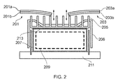
- FIG. 2 is a schematic representation of apparatus according to an example.
- Bimetallic structures 201, 203 comprising first 201a, 203a and second 201b, 203b metallic layers with respective different coefficients of thermal expansion are provided.
- the bimetallic structures 201, 203 are configured to exert pressure on at least one heat sink 205 arranged on a housing 207 whereby to dissipate heat from the electronic device 209.
- the heat sink 205 is held in place on the housing 207 using a clip 208, which, in an example, can be a standard heat sink clip.
- the clip 208 generally contacts, and pushes down on, the heat sink 205.
- a thermal interface material 213 can be disposed between the heat sink 205 and the electronic package being cooled.
- the electronic package is the combination of the electronic device 209 within the housing 207, but in some examples may just be an electronic device 209.
- the bimetallic elements 201, 203 are employed to exert a force on the heat sink 205 and decrease the thermal resistance between the heat sink 205 and a heat source, which in the case of figure 2 is the electronic device (optical module) 209, which is provided on a base structure 211.
- Additional bimetallic structures can be arranged over "hot spots" in the electronic package or at other points on the clip 208 such that the clip 208 will bend in such a way to add more pressure to the "hot spots”.
- the bimetallic elements are configured to deflect according to the temperature of the electronic device.
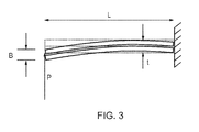
- figure 3 which is a schematic representation of a bimetallic structure of length L and thickness t
- the following equations can be used to design a bimetallic structure in order to induce a desired amount of deflection whereby to exert a desired level of force upon a heat sink or hot zone.
- a desired force to be exerted by a bimetallic structure can be set according to various parameters of the structure that can be selected taking into account the expected temperature range of the electronic device in question. For example, as noted above, when the temperature of the structure drops below or is at a certain level T 1 , the bimetallic structure will not exert any pressure on the heatsink (such as being in a rest configuration in which it is just in contact with the heatsink or is displaced from the heatsink) allowing the module to be removed or replaced easily. When the temperature of the module increases, the bimetallic strip exerts a contact force that increases in proportion to the temperature increase. The higher pressure ensures a better thermal interface, ultimately higher heat transfer rates and improved product performance.
- An example use case is for a bi-metallic heat sink clip incorporating a cantilever type bimetallic structure that is flat at typical room temperature of 22 °C (T 1 ).
- T 1 typical room temperature of 22 °C
- T 2 typical room temperature of 22 °C
- the dimensions could be 3 mm thick, 5 mm in width and 25 mm long.
- a typical bimetallic beam from a commercial supplier has an elastic modulus of approximately 135 N/mm 2 and has a specific deflection of 2.08E-05 K -1 . Such a beam would apply approximately 35 N to the heat sink clip, which would increase the contact pressure and decrease the thermal resistance between the optical module and the heat sink.
- FIG. 4 is a schematic representation of a clip according to an example.
- bimetallic structures 401-405 are integrated into the clip 407 to exert a force on a heat sink and decrease the thermal resistance between the heat sink and heat source (not shown). This forms a bimetallic clip structure 400. As the temperature of the electronic device increases, the bimetallic structures bend as shown, whereby to exert a downward compression (direction A) upon a heat sink and heat source.
- the clip can be formed using one type of metal and a second metal layer with a different thermal expansion coefficient can be bonded to the clip in specific locations in order to provide bimetallic structures at those locations.
- the locations can be determined such that the deflection of the clip when heated compresses or extends the material of the clip so that a heat sink is forced down onto the hot component/optical module.
- FIG. 5 is a schematic representation of a clip according to an example.
- one or more smaller bimetallic structures 501, 503 can be provided at known hot spots of an electronic device or package 505 in order to target problem areas that are known to suffer from significant heat issues.
- the temperature of this region can be regulated using a bimetallic structure 501 (and/or 503) in order to provide localized compression or localized exertion of a force that can be used in unison with an associated heat sink to enable more efficient dissipation of heat from the region.
- the clip with integrated bimetallic structures forms a bimetallic clip structure 500.
- a compressible TIM (thermal interface material) 507 can be used at the interface between the clip and/or bimetallic structure and the housing 509.
- the TIM will compress most under the bimetallic elements affording increased heat flux removal at the hot spots.
- a heat-sink can be integrated with a bimetallic clip structure as one single part. This would allow improved performance of the hot spot targeting element of the device.
- a heat sink instead of being a structure that is held in place by a clip, a heat sink can be directly attached or otherwise part of a bimetallic structure.
Landscapes
- Cooling Or The Like Of Electrical Apparatus (AREA)
Abstract
Description
- Aspects relate, in general to an apparatus for regulating the temperature of an electronic package, a method and an assembly.
- Heat regulation of electronic devices is an important and challenging area. As devices become denser and the demands on equipment increases, the heat produced by devices can be significant and detrimentally effect operation and efficiency. For example, heat generated in optical/electronic interface devices, such as XFPs, SFPs and CFPs and so on must find a path to the surrounding air. Typically, around 50% of the thermal resistance between a high temperature optical/electronic interface device and the cooler ambient air is due to the contact resistance between the device and its heat sink
- Contact between the device and the heat sink is currently made using a spring loaded clip. However, this does not typically supply enough pressure between the two components to achieve sufficiently low thermal resistances. This means that heat typically cannot be removed from the device quickly enough for future densely packed optical equipment to be viable. This is particularly challenging to address since the temperature of the device must typically be held below a certain level using a design that allows it to be easily plugged/unplugged for maintenance and repair without using specialised tooling or thermal pastes. As noted, overheating of devices is a limiting factor of telecom routing equipment as data rates move to 400 and ultimately to 1000 Gb/s for example.
- According to an example, there is provided an apparatus for regulating the temperature of an electronic package, the apparatus comprising a clip configured to receive the electronic package and maintain a heat sink in thermal contact with the electronic package, at least one bimetallic structure comprising first and second metallic layers with respective different coefficients of thermal expansion, the bimetallic structure being configured to elastically deform to exert pressure on the heat sink in response to an increase in temperature whereby to dissipate heat from the electronic package. The bimetallic structure can be integrated in at least one side of a clip being configured to releasably secure the package. At least one leg can depend from the periphery of a generally flat portion, wherein the at least one leg includes at least one bimetallic structure comprising first and second metallic layers with respective different coefficients of thermal expansion, the at least one leg being configured to cause deformation in the clip when the leg is subjected to heat. A compressible thermal interface material can be arranged between the at least one heat sink and the electronic package at a specific location or in multiple locations. The generally flat portion can include multiple bimetallic structures arranged over a predetermined region of the electronic package, heat sink or a thermal interface material. The at least one bimetallic structure can be configured elastically deform to exert or increase a contact pressure between the heat sink and at least a portion of the housing and/or a thermal interface material above a predetermined threshold temperature. The clip can comprise multiple arms extending from the generally flat portion between a pair of legs or multiple legs extending from the periphery thereof. At least one of the arms can include an inwardly extending, generally central region.
- According to an example, there is provided a method for regulating the temperature of an electronic package, the method comprising securing a heat sink to or arranging a heat sink over at least a portion of the electronic package using a clip configured to receive the electronic package and maintain the heat sink in thermal contact with the electronic package, increasing contact pressure between the heat sink and at least a portion of the electronic package by elastically deforming the clip using at least one bimetallic structure comprising first and second metallic layers with respective different coefficients of thermal expansion, in response to raising the temperature of the or each bimetallic structure above a threshold temperature whereby to improve heat transfer from the electronic package. The first and second metallic layers can be so selected as to form a bimetallic structure being operable to exert or increase a contact pressure between the heat sink and at least a portion of the housing and/or a thermal interface material when the temperature of the structure reaches the threshold temperature. A compressible thermal interface material can be provided at least between the heat sink and the electronic package.
- According to an example, there is provided an assembly comprising an electronic package, the package secured to a base structure of the assembly and comprising at least one opening to receive a heat sink secured to the electronic package using a clip configured to receive the electronic package and maintain the heat sink in thermal contact with the electronic package, the assembly further comprising a portion including at least one bimetallic structure comprising first and second metallic layers with respective different coefficients of thermal expansion. The clip can further comprise at least one leg depending from the periphery of a generally flat portion, wherein the or each leg includes at least one bimetallic structure comprising first and second metallic layers with respective different coefficients of thermal expansion, the at least one leg being configured to induce compression of the clip when the leg is subjected to heat. A compressible thermal interface material can be arranged between the at least one heat sink and the electronic package, at a specific location or in multiple locations. The clip can further comprise multiple arms extending between a pair of legs or multiple legs extending from the periphery of the generally flat portion. The electronic package can comprise an electronic device received within a housing, wherein the housing includes the at least one opening.
- Embodiments will now be described, by way of example only, with reference to the accompanying drawings, in which:
-
Figure 1 is an exemplary schematic representation of an existing XFP clip; -
Figure 2 is a schematic representation of a clip according to an example; -
Figure 3 is a schematic representation of a bimetallic structure of length L and thickness t according to an example; -
Figure 4 is a schematic representation of a clip according to an example; and -
Figure 5 is a schematic representation of a clip according to an example. - Example embodiments are described below in sufficient detail to enable those of ordinary skill in the art to embody and implement the systems and processes herein described. It is important to understand that embodiments can be provided in many alternate forms and should not be construed as limited to the examples set forth herein.
- Accordingly, while embodiments can be modified in various ways and take on various alternative forms, specific embodiments thereof are shown in the drawings and described in detail below as examples. There is no intent to limit to the particular forms disclosed. On the contrary, all modifications, equivalents, and alternatives falling within the scope of the appended claims should be included. Elements of the example embodiments are consistently denoted by the same reference numerals throughout the drawings and detailed description where appropriate.
- The terminology used herein to describe embodiments is not intended to limit the scope. The articles "a," "an," and "the" are singular in that they have a single referent, however the use of the singular form in the present document should not preclude the presence of more than one referent. In other words, elements referred to in the singular can number one or more, unless the context clearly indicates otherwise. It will be further understood that the terms "comprises," "comprising," "includes," and/or "including," when used herein, specify the presence of stated features, items, steps, operations, elements, and/or components, but do not preclude the presence or addition of one or more other features, items, steps, operations, elements, components, and/or groups thereof.
- Unless otherwise defined, all terms (including technical and scientific terms) used herein are to be interpreted as is customary in the art. It will be further understood that terms in common usage should also be interpreted as is customary in the relevant art and not in an idealized or overly formal sense unless expressly so defined herein.
- Large numbers of devices, such as optical components in a telecommunications network infrastructure for example, use slot based input/output connectors in a face plate. These connections link the voice/data traffic from the network to optical or electrical modules on the main board where processing occurs. For ease of use, the connectors are typically field replaceable. That is, an operator can remove the device for replacement or repair without the use of specialised tooling. Generally, in order to accomplish this, modules slide into a housing or casing on a main circuit board or base structure and are connected to a heat sink using a metal spring. The spring force generated cannot be too large or the connectors would not be easily replaced. In addition, typically no thermal grease or other interface material is used between the module and the heat sink. This combination of low spring force and "dry" contact leads to a large thermal barrier between the optical module and the heat sink, which ultimately means the connector modules overheat often. This can affect product releases and/or increase product return rates. In general, the more devices on the face plate, the bigger the issue, which is especially important when one considers higher data rate products which require more densely packed input/output connectors.
- According to an example, apparatus for regulating the temperature of an electronic device in a housing is provided. The apparatus includes a top portion including at least one bimetallic strip, which acts as an active component that bends or deflects according to temperature changes. For example, in the presence of heat, such that the temperature of the top portion exceeds a threshold temperature, the strip can deflect so as to increase the contact pressure between a heat sink and a device mounted in a housing, thus decreasing the thermal resistance with increasing temperature. In an example, the bimetallic strip comprises first and second metallic layers with respective different coefficients of thermal expansion so selected as to exert a pressure that is proportional to the temperature increase, thereby allowing more efficient cooling of the device, which can be an optical module for example, and this increases performance.
- A compressible thermal interface material may also be employed between the heat sink and the heat source. As the temperature of the heat source increases, the bimetallic heat sink clip imparts proportionally higher pressure and compresses the thermal interface material, thus reducing the thermal resistance, allowing for increased performance.
- The bimetallic strip contains two different materials that are bonded together. Due to the difference in mechanical properties between the materials used, the strip can be configured to deflect dependent on the surrounding temperature. The level of deflection and induced force from the strip is proportional to the temperature increase. The bimetallic strip can be designed to operate within the expected temperature range of the device in question, such as an optical module for example. When the temperature drops below a certain threshold level, the bimetallic strip will not exert any pressure on a heatsink allowing the module to be removed or replaced easily. When the temperature of the module increases, the bimetallic strip can be selected or configured so as to exert a contact force that increases in proportion to the temperature increase. The higher pressure ensures a better thermal interface, ultimately higher heat transfer rates and improved product performance.
- That is, a strip can be configured so that it does not contact a heat sink until a threshold temperature has been reached for example. Accordingly, the strip would need to get to a specific temperature before it covered the distance from its rest position to the heat sink or before the force on a heat sink builds sufficiently for the clip to exert pressure on the heat sink causing it to contact a device or device housing (or causing an increase in the applied pressure on the device or device housing in the case that the strip is in contact with the heat sink when at rest). Some bimetallic structures can 'snap' through to different positions at specific temperatures. These have a threshold temperature of operation that leads to a specific configuration of the strip, the value of which would depend on the structures design (thicknesses of metal layers and shape of the structure) and this could be tailored to specific applications.
- Thus, enhanced heat transfer from a heat sink that cools, for example, an optical interface module can be provided. This enhanced heat transfer leads to reduced overheating events in these optical modules which increases the reliability of the devices and reduces the return rate of these components. Additionally, this allows denser packing of optical modules in equipment. Currently densely packed optical modules suffer since the cumulative thermal loads of the devices can cause them to exceed design guidelines and can lead to increased failure rates. Enhanced heat transfer rates allow more effective cooling of electronic devices and enable equipment with more densely packed optical modules to be realised.
-
Figure 1 is an exemplary schematic representation of an existing XFP clip. XFP (I0 Gigabit Small Form Factor Pluggable) is a standard for transceivers used in high-speed network and telecommunication links that use optical fiber. The clip is typically made from copper, stainless steel or aluminium. The shape is such that pressure is applied to the heat sink when an optical module is inserted. Mounting points enable the clip to be mounted to a base structure, and in the example offigure 1 , the clip includes three top portions that exert a pressure against a device that is inserted into a housing. Typically, the housing includes a number of openings or windows. Respective top portions are arranged over the openings, and a heat sink arranged on the device protrudes through an opening and is held in place by a top portion. - The XFP clip is therefore in the form of a standard metal clip that is used to hold down a heat sink on an optical module. This is not an effective solution since the clip does not offer sufficient clamping pressure and leads to very high thermal resistance between the heat sink and the electronic device. The effect of increased thermal resistance is increased temperature in the optical module and reduced reliability of the optical equipment and network quality of service. The proposed solution offers significantly increased clamping pressure with increasing temperature that reduces this thermal resistance and enhances the reliability of electronic devices. By increasing the thermal performance of each electronic device individually more of these devices can be packed together increasing the number of devices per unit area in equipment.
-
Figure 2 is a schematic representation of apparatus according to an example. Bimetallicstructures bimetallic structures heat sink 205 arranged on ahousing 207 whereby to dissipate heat from theelectronic device 209. Theheat sink 205 is held in place on thehousing 207 using aclip 208, which, in an example, can be a standard heat sink clip. Theclip 208 generally contacts, and pushes down on, theheat sink 205. Optionally, athermal interface material 213 can be disposed between theheat sink 205 and the electronic package being cooled. In this context, the electronic package is the combination of theelectronic device 209 within thehousing 207, but in some examples may just be anelectronic device 209. - Thus, the
bimetallic elements heat sink 205 and decrease the thermal resistance between theheat sink 205 and a heat source, which in the case offigure 2 is the electronic device (optical module) 209, which is provided on abase structure 211. - Additional bimetallic structures can be arranged over "hot spots" in the electronic package or at other points on the
clip 208 such that theclip 208 will bend in such a way to add more pressure to the "hot spots". - The bimetallic elements are configured to deflect according to the temperature of the electronic device. According to an example, and with reference to
figure 3 , which is a schematic representation of a bimetallic structure of length L and thickness t, the following equations can be used to design a bimetallic structure in order to induce a desired amount of deflection whereby to exert a desired level of force upon a heat sink or hot zone. - The thermal (linear) deflection, B, is calculated as follows:

where t = material thickness, (T2-T1) = temperature change, L= active length of bimetallic structure and a = specific deflection. - The mechanical force, P, induced by a bimetallic structure is:
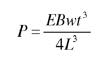
where E = elastic modulus and w = material width. - The thermal force, P, is therefore:

- Accordingly, a desired force to be exerted by a bimetallic structure can be set according to various parameters of the structure that can be selected taking into account the expected temperature range of the electronic device in question. For example, as noted above, when the temperature of the structure drops below or is at a certain level T1, the bimetallic structure will not exert any pressure on the heatsink (such as being in a rest configuration in which it is just in contact with the heatsink or is displaced from the heatsink) allowing the module to be removed or replaced easily. When the temperature of the module increases, the bimetallic strip exerts a contact force that increases in proportion to the temperature increase. The higher pressure ensures a better thermal interface, ultimately higher heat transfer rates and improved product performance.
- An example use case is for a bi-metallic heat sink clip incorporating a cantilever type bimetallic structure that is flat at typical room temperature of 22 °C (T1). Consider that the beam is expected to rise to approximately 50 °C (T2) when in contact with a heated optical module for example. The dimensions could be 3 mm thick, 5 mm in width and 25 mm long. A typical bimetallic beam from a commercial supplier has an elastic modulus of approximately 135 N/mm2 and has a specific deflection of 2.08E-05 K-1. Such a beam would apply approximately 35 N to the heat sink clip, which would increase the contact pressure and decrease the thermal resistance between the optical module and the heat sink.
-
Figure 4 is a schematic representation of a clip according to an example. In the example offigure 4 , bimetallic structures 401-405 are integrated into theclip 407 to exert a force on a heat sink and decrease the thermal resistance between the heat sink and heat source (not shown). This forms abimetallic clip structure 400. As the temperature of the electronic device increases, the bimetallic structures bend as shown, whereby to exert a downward compression (direction A) upon a heat sink and heat source. - For example, the clip can be formed using one type of metal and a second metal layer with a different thermal expansion coefficient can be bonded to the clip in specific locations in order to provide bimetallic structures at those locations. The locations can be determined such that the deflection of the clip when heated compresses or extends the material of the clip so that a heat sink is forced down onto the hot component/optical module.
-
Figure 5 is a schematic representation of a clip according to an example. In the example offigure 5 , one or more smallerbimetallic structures package 505 in order to target problem areas that are known to suffer from significant heat issues. For example, it may be well known that a certain region of an electronic device experiences, in use, higher temperatures than other regions of the device due to, for example, the layout of internal components and/or the inability for an unimpeded airflow within that portion of the device. Accordingly, the temperature of this region can be regulated using a bimetallic structure 501 (and/or 503) in order to provide localized compression or localized exertion of a force that can be used in unison with an associated heat sink to enable more efficient dissipation of heat from the region. The clip with integrated bimetallic structures forms abimetallic clip structure 500. - A compressible TIM (thermal interface material) 507 can be used at the interface between the clip and/or bimetallic structure and the
housing 509. The TIM will compress most under the bimetallic elements affording increased heat flux removal at the hot spots. - According to an example, a heat-sink can be integrated with a bimetallic clip structure as one single part. This would allow improved performance of the hot spot targeting element of the device. For example, instead of being a structure that is held in place by a clip, a heat sink can be directly attached or otherwise part of a bimetallic structure.
- The present inventions can be embodied in other specific apparatus and/or methods. The described embodiments are to be considered in all respects as illustrative and not restrictive. In particular, the scope of the invention is indicated by the appended claims rather than by the description and figures herein. All changes that come within the meaning and range of equivalency of the claims are to be embraced within their scope.
Claims (16)
Priority Applications (1)
| Application Number | Priority Date | Filing Date | Title |
|---|---|---|---|
| EP15306616.2A EP3157054B1 (en) | 2015-10-13 | 2015-10-13 | Apparatus for regulating the temperature of an electronic device in a housing, a method and an assembly |
Applications Claiming Priority (1)
| Application Number | Priority Date | Filing Date | Title |
|---|---|---|---|
| EP15306616.2A EP3157054B1 (en) | 2015-10-13 | 2015-10-13 | Apparatus for regulating the temperature of an electronic device in a housing, a method and an assembly |
Publications (2)
| Publication Number | Publication Date |
|---|---|
| EP3157054A1 true EP3157054A1 (en) | 2017-04-19 |
| EP3157054B1 EP3157054B1 (en) | 2021-03-24 |
Family
ID=54337710
Family Applications (1)
| Application Number | Title | Priority Date | Filing Date |
|---|---|---|---|
| EP15306616.2A Active EP3157054B1 (en) | 2015-10-13 | 2015-10-13 | Apparatus for regulating the temperature of an electronic device in a housing, a method and an assembly |
Country Status (1)
| Country | Link |
|---|---|
| EP (1) | EP3157054B1 (en) |
Cited By (2)
| Publication number | Priority date | Publication date | Assignee | Title |
|---|---|---|---|---|
| US12074081B2 (en) * | 2021-05-28 | 2024-08-27 | Cisco Technology, Inc. | Use of bimetals in a heat sink to benefit heat transfer from high temperature integrated circuit components on a circuit board |
| US12213276B2 (en) | 2022-08-31 | 2025-01-28 | Cisco Technology, Inc. | Intelligent dynamic air baffle |
Citations (5)
| Publication number | Priority date | Publication date | Assignee | Title |
|---|---|---|---|---|
| DE19537633A1 (en) * | 1995-10-10 | 1997-04-17 | Daimler Benz Aerospace Ag | Heat conductor device for connection between component and heat sink |
| EP0852398A1 (en) * | 1997-01-02 | 1998-07-08 | AT&T Corp. | Apparatus for heating and cooling an electronic device |
| US6545352B1 (en) * | 2002-02-15 | 2003-04-08 | Ericsson Inc. | Assembly for mounting power semiconductive modules to heat dissipators |
| US6894908B1 (en) * | 2003-03-28 | 2005-05-17 | Intel Corporation | Bridge clip with bimetallic leaf and method |
| DE102006037747A1 (en) * | 2006-08-11 | 2008-03-13 | Nokia Siemens Networks Gmbh & Co.Kg | Cooling device for electrical element, comprises carrier to connect with electrical element, where another cooling device is mounted to cooling device in temperature dependent and movable manner |
Family Cites Families (1)
| Publication number | Priority date | Publication date | Assignee | Title |
|---|---|---|---|---|
| EP0673065A1 (en) * | 1994-03-16 | 1995-09-20 | Siemens Nixdorf Informationssysteme AG | Cooling device for electronic components |
-
2015
- 2015-10-13 EP EP15306616.2A patent/EP3157054B1/en active Active
Patent Citations (5)
| Publication number | Priority date | Publication date | Assignee | Title |
|---|---|---|---|---|
| DE19537633A1 (en) * | 1995-10-10 | 1997-04-17 | Daimler Benz Aerospace Ag | Heat conductor device for connection between component and heat sink |
| EP0852398A1 (en) * | 1997-01-02 | 1998-07-08 | AT&T Corp. | Apparatus for heating and cooling an electronic device |
| US6545352B1 (en) * | 2002-02-15 | 2003-04-08 | Ericsson Inc. | Assembly for mounting power semiconductive modules to heat dissipators |
| US6894908B1 (en) * | 2003-03-28 | 2005-05-17 | Intel Corporation | Bridge clip with bimetallic leaf and method |
| DE102006037747A1 (en) * | 2006-08-11 | 2008-03-13 | Nokia Siemens Networks Gmbh & Co.Kg | Cooling device for electrical element, comprises carrier to connect with electrical element, where another cooling device is mounted to cooling device in temperature dependent and movable manner |
Cited By (2)
| Publication number | Priority date | Publication date | Assignee | Title |
|---|---|---|---|---|
| US12074081B2 (en) * | 2021-05-28 | 2024-08-27 | Cisco Technology, Inc. | Use of bimetals in a heat sink to benefit heat transfer from high temperature integrated circuit components on a circuit board |
| US12213276B2 (en) | 2022-08-31 | 2025-01-28 | Cisco Technology, Inc. | Intelligent dynamic air baffle |
Also Published As
| Publication number | Publication date |
|---|---|
| EP3157054B1 (en) | 2021-03-24 |
Similar Documents
| Publication | Publication Date | Title |
|---|---|---|
| US10617034B2 (en) | Heat dissipation system of enclosed electronic module with single/multiple active components | |
| US9841772B2 (en) | Temperature responsive thermal bridge | |
| CN113966648B (en) | Heat dissipation | |
| JP5082970B2 (en) | Circuit board equipment | |
| EP2738804B1 (en) | Flexible thermal transfer strips | |
| US10631438B2 (en) | Mechanically flexible cold plates for low power components | |
| CA1228173A (en) | Cooling system for electronic circuit device | |
| US5848083A (en) | Expansion-matched high-thermal-conductivity stress-relieved mounting modules | |
| US7468890B2 (en) | Graphics card heat-dissipating device | |
| US20080310119A1 (en) | Clip on heat sink | |
| JP6036894B2 (en) | Cooling device and equipment | |
| US10806054B1 (en) | Flexible elastic thermal bridge for electronic subassemblies with variable gaps between components and enclosures | |
| JPH10200208A (en) | Semiconductor laser module | |
| US20210325616A1 (en) | Pluggable optical module cage for fixed heat sink | |
| JP6500450B2 (en) | Heat dissipation method and heat dissipation device | |
| WO2015198642A1 (en) | Heat sink and method for dissipating heat using heat sink | |
| JPH04263456A (en) | Product provided with heat sink | |
| JPS6323660B2 (en) | ||
| TWI658476B (en) | Coil device | |
| JP7110599B2 (en) | Electronics | |
| EP3050411B1 (en) | Fixation of heat sink on sfp/xfp cage | |
| EP3157054B1 (en) | Apparatus for regulating the temperature of an electronic device in a housing, a method and an assembly | |
| CN116500731A (en) | optical transceiver | |
| EP2775732A1 (en) | Protection device for a contact strip of a distribution device | |
| US20200329551A1 (en) | Heat sink fixing member and electronic device |
Legal Events
| Date | Code | Title | Description |
|---|---|---|---|
| PUAI | Public reference made under article 153(3) epc to a published international application that has entered the european phase |
Free format text: ORIGINAL CODE: 0009012 |
|
| STAA | Information on the status of an ep patent application or granted ep patent |
Free format text: STATUS: THE APPLICATION HAS BEEN PUBLISHED |
|
| AK | Designated contracting states |
Kind code of ref document: A1 Designated state(s): AL AT BE BG CH CY CZ DE DK EE ES FI FR GB GR HR HU IE IS IT LI LT LU LV MC MK MT NL NO PL PT RO RS SE SI SK SM TR |
|
| AX | Request for extension of the european patent |
Extension state: BA ME |
|
| STAA | Information on the status of an ep patent application or granted ep patent |
Free format text: STATUS: REQUEST FOR EXAMINATION WAS MADE |
|
| 17P | Request for examination filed |
Effective date: 20171019 |
|
| RBV | Designated contracting states (corrected) |
Designated state(s): AL AT BE BG CH CY CZ DE DK EE ES FI FR GB GR HR HU IE IS IT LI LT LU LV MC MK MT NL NO PL PT RO RS SE SI SK SM TR |
|
| STAA | Information on the status of an ep patent application or granted ep patent |
Free format text: STATUS: EXAMINATION IS IN PROGRESS |
|
| 17Q | First examination report despatched |
Effective date: 20180115 |
|
| RAP1 | Party data changed (applicant data changed or rights of an application transferred) |
Owner name: ALCATEL LUCENT |
|
| GRAP | Despatch of communication of intention to grant a patent |
Free format text: ORIGINAL CODE: EPIDOSNIGR1 |
|
| STAA | Information on the status of an ep patent application or granted ep patent |
Free format text: STATUS: GRANT OF PATENT IS INTENDED |
|
| INTG | Intention to grant announced |
Effective date: 20201105 |
|
| GRAS | Grant fee paid |
Free format text: ORIGINAL CODE: EPIDOSNIGR3 |
|
| GRAA | (expected) grant |
Free format text: ORIGINAL CODE: 0009210 |
|
| STAA | Information on the status of an ep patent application or granted ep patent |
Free format text: STATUS: THE PATENT HAS BEEN GRANTED |
|
| AK | Designated contracting states |
Kind code of ref document: B1 Designated state(s): AL AT BE BG CH CY CZ DE DK EE ES FI FR GB GR HR HU IE IS IT LI LT LU LV MC MK MT NL NO PL PT RO RS SE SI SK SM TR |
|
| REG | Reference to a national code |
Ref country code: GB Ref legal event code: FG4D |
|
| REG | Reference to a national code |
Ref country code: CH Ref legal event code: EP |
|
| REG | Reference to a national code |
Ref country code: DE Ref legal event code: R096 Ref document number: 602015067172 Country of ref document: DE |
|
| REG | Reference to a national code |
Ref country code: IE Ref legal event code: FG4D |
|
| REG | Reference to a national code |
Ref country code: AT Ref legal event code: REF Ref document number: 1375358 Country of ref document: AT Kind code of ref document: T Effective date: 20210415 |
|
| REG | Reference to a national code |
Ref country code: LT Ref legal event code: MG9D |
|
| PG25 | Lapsed in a contracting state [announced via postgrant information from national office to epo] |
Ref country code: HR Free format text: LAPSE BECAUSE OF FAILURE TO SUBMIT A TRANSLATION OF THE DESCRIPTION OR TO PAY THE FEE WITHIN THE PRESCRIBED TIME-LIMIT Effective date: 20210324 Ref country code: FI Free format text: LAPSE BECAUSE OF FAILURE TO SUBMIT A TRANSLATION OF THE DESCRIPTION OR TO PAY THE FEE WITHIN THE PRESCRIBED TIME-LIMIT Effective date: 20210324 Ref country code: GR Free format text: LAPSE BECAUSE OF FAILURE TO SUBMIT A TRANSLATION OF THE DESCRIPTION OR TO PAY THE FEE WITHIN THE PRESCRIBED TIME-LIMIT Effective date: 20210625 Ref country code: BG Free format text: LAPSE BECAUSE OF FAILURE TO SUBMIT A TRANSLATION OF THE DESCRIPTION OR TO PAY THE FEE WITHIN THE PRESCRIBED TIME-LIMIT Effective date: 20210624 Ref country code: NO Free format text: LAPSE BECAUSE OF FAILURE TO SUBMIT A TRANSLATION OF THE DESCRIPTION OR TO PAY THE FEE WITHIN THE PRESCRIBED TIME-LIMIT Effective date: 20210624 |
|
| PG25 | Lapsed in a contracting state [announced via postgrant information from national office to epo] |
Ref country code: LV Free format text: LAPSE BECAUSE OF FAILURE TO SUBMIT A TRANSLATION OF THE DESCRIPTION OR TO PAY THE FEE WITHIN THE PRESCRIBED TIME-LIMIT Effective date: 20210324 Ref country code: RS Free format text: LAPSE BECAUSE OF FAILURE TO SUBMIT A TRANSLATION OF THE DESCRIPTION OR TO PAY THE FEE WITHIN THE PRESCRIBED TIME-LIMIT Effective date: 20210324 Ref country code: SE Free format text: LAPSE BECAUSE OF FAILURE TO SUBMIT A TRANSLATION OF THE DESCRIPTION OR TO PAY THE FEE WITHIN THE PRESCRIBED TIME-LIMIT Effective date: 20210324 |
|
| REG | Reference to a national code |
Ref country code: NL Ref legal event code: MP Effective date: 20210324 |
|
| REG | Reference to a national code |
Ref country code: AT Ref legal event code: MK05 Ref document number: 1375358 Country of ref document: AT Kind code of ref document: T Effective date: 20210324 |
|
| PG25 | Lapsed in a contracting state [announced via postgrant information from national office to epo] |
Ref country code: NL Free format text: LAPSE BECAUSE OF FAILURE TO SUBMIT A TRANSLATION OF THE DESCRIPTION OR TO PAY THE FEE WITHIN THE PRESCRIBED TIME-LIMIT Effective date: 20210324 |
|
| PG25 | Lapsed in a contracting state [announced via postgrant information from national office to epo] |
Ref country code: SM Free format text: LAPSE BECAUSE OF FAILURE TO SUBMIT A TRANSLATION OF THE DESCRIPTION OR TO PAY THE FEE WITHIN THE PRESCRIBED TIME-LIMIT Effective date: 20210324 Ref country code: AT Free format text: LAPSE BECAUSE OF FAILURE TO SUBMIT A TRANSLATION OF THE DESCRIPTION OR TO PAY THE FEE WITHIN THE PRESCRIBED TIME-LIMIT Effective date: 20210324 Ref country code: LT Free format text: LAPSE BECAUSE OF FAILURE TO SUBMIT A TRANSLATION OF THE DESCRIPTION OR TO PAY THE FEE WITHIN THE PRESCRIBED TIME-LIMIT Effective date: 20210324 Ref country code: CZ Free format text: LAPSE BECAUSE OF FAILURE TO SUBMIT A TRANSLATION OF THE DESCRIPTION OR TO PAY THE FEE WITHIN THE PRESCRIBED TIME-LIMIT Effective date: 20210324 Ref country code: EE Free format text: LAPSE BECAUSE OF FAILURE TO SUBMIT A TRANSLATION OF THE DESCRIPTION OR TO PAY THE FEE WITHIN THE PRESCRIBED TIME-LIMIT Effective date: 20210324 |
|
| PG25 | Lapsed in a contracting state [announced via postgrant information from national office to epo] |
Ref country code: IS Free format text: LAPSE BECAUSE OF FAILURE TO SUBMIT A TRANSLATION OF THE DESCRIPTION OR TO PAY THE FEE WITHIN THE PRESCRIBED TIME-LIMIT Effective date: 20210724 Ref country code: PT Free format text: LAPSE BECAUSE OF FAILURE TO SUBMIT A TRANSLATION OF THE DESCRIPTION OR TO PAY THE FEE WITHIN THE PRESCRIBED TIME-LIMIT Effective date: 20210726 Ref country code: PL Free format text: LAPSE BECAUSE OF FAILURE TO SUBMIT A TRANSLATION OF THE DESCRIPTION OR TO PAY THE FEE WITHIN THE PRESCRIBED TIME-LIMIT Effective date: 20210324 Ref country code: ES Free format text: LAPSE BECAUSE OF FAILURE TO SUBMIT A TRANSLATION OF THE DESCRIPTION OR TO PAY THE FEE WITHIN THE PRESCRIBED TIME-LIMIT Effective date: 20210324 Ref country code: SK Free format text: LAPSE BECAUSE OF FAILURE TO SUBMIT A TRANSLATION OF THE DESCRIPTION OR TO PAY THE FEE WITHIN THE PRESCRIBED TIME-LIMIT Effective date: 20210324 Ref country code: RO Free format text: LAPSE BECAUSE OF FAILURE TO SUBMIT A TRANSLATION OF THE DESCRIPTION OR TO PAY THE FEE WITHIN THE PRESCRIBED TIME-LIMIT Effective date: 20210324 |
|
| REG | Reference to a national code |
Ref country code: DE Ref legal event code: R097 Ref document number: 602015067172 Country of ref document: DE |
|
| PG25 | Lapsed in a contracting state [announced via postgrant information from national office to epo] |
Ref country code: DK Free format text: LAPSE BECAUSE OF FAILURE TO SUBMIT A TRANSLATION OF THE DESCRIPTION OR TO PAY THE FEE WITHIN THE PRESCRIBED TIME-LIMIT Effective date: 20210324 Ref country code: AL Free format text: LAPSE BECAUSE OF FAILURE TO SUBMIT A TRANSLATION OF THE DESCRIPTION OR TO PAY THE FEE WITHIN THE PRESCRIBED TIME-LIMIT Effective date: 20210324 |
|
| PLBE | No opposition filed within time limit |
Free format text: ORIGINAL CODE: 0009261 |
|
| STAA | Information on the status of an ep patent application or granted ep patent |
Free format text: STATUS: NO OPPOSITION FILED WITHIN TIME LIMIT |
|
| PG25 | Lapsed in a contracting state [announced via postgrant information from national office to epo] |
Ref country code: SI Free format text: LAPSE BECAUSE OF FAILURE TO SUBMIT A TRANSLATION OF THE DESCRIPTION OR TO PAY THE FEE WITHIN THE PRESCRIBED TIME-LIMIT Effective date: 20210324 |
|
| 26N | No opposition filed |
Effective date: 20220104 |
|
| REG | Reference to a national code |
Ref country code: CH Ref legal event code: PL |
|
| PG25 | Lapsed in a contracting state [announced via postgrant information from national office to epo] |
Ref country code: IS Free format text: LAPSE BECAUSE OF FAILURE TO SUBMIT A TRANSLATION OF THE DESCRIPTION OR TO PAY THE FEE WITHIN THE PRESCRIBED TIME-LIMIT Effective date: 20210724 |
|
| REG | Reference to a national code |
Ref country code: BE Ref legal event code: MM Effective date: 20211031 |
|
| PG25 | Lapsed in a contracting state [announced via postgrant information from national office to epo] |
Ref country code: MC Free format text: LAPSE BECAUSE OF FAILURE TO SUBMIT A TRANSLATION OF THE DESCRIPTION OR TO PAY THE FEE WITHIN THE PRESCRIBED TIME-LIMIT Effective date: 20210324 |
|
| PG25 | Lapsed in a contracting state [announced via postgrant information from national office to epo] |
Ref country code: LU Free format text: LAPSE BECAUSE OF NON-PAYMENT OF DUE FEES Effective date: 20211013 Ref country code: BE Free format text: LAPSE BECAUSE OF NON-PAYMENT OF DUE FEES Effective date: 20211031 |
|
| PG25 | Lapsed in a contracting state [announced via postgrant information from national office to epo] |
Ref country code: LI Free format text: LAPSE BECAUSE OF NON-PAYMENT OF DUE FEES Effective date: 20211031 Ref country code: CH Free format text: LAPSE BECAUSE OF NON-PAYMENT OF DUE FEES Effective date: 20211031 |
|
| PG25 | Lapsed in a contracting state [announced via postgrant information from national office to epo] |
Ref country code: FR Free format text: LAPSE BECAUSE OF NON-PAYMENT OF DUE FEES Effective date: 20211031 |
|
| PG25 | Lapsed in a contracting state [announced via postgrant information from national office to epo] |
Ref country code: IE Free format text: LAPSE BECAUSE OF NON-PAYMENT OF DUE FEES Effective date: 20211013 |
|
| PG25 | Lapsed in a contracting state [announced via postgrant information from national office to epo] |
Ref country code: IT Free format text: LAPSE BECAUSE OF FAILURE TO SUBMIT A TRANSLATION OF THE DESCRIPTION OR TO PAY THE FEE WITHIN THE PRESCRIBED TIME-LIMIT Effective date: 20210324 |
|
| PG25 | Lapsed in a contracting state [announced via postgrant information from national office to epo] |
Ref country code: HU Free format text: LAPSE BECAUSE OF FAILURE TO SUBMIT A TRANSLATION OF THE DESCRIPTION OR TO PAY THE FEE WITHIN THE PRESCRIBED TIME-LIMIT; INVALID AB INITIO Effective date: 20151013 |
|
| PG25 | Lapsed in a contracting state [announced via postgrant information from national office to epo] |
Ref country code: CY Free format text: LAPSE BECAUSE OF FAILURE TO SUBMIT A TRANSLATION OF THE DESCRIPTION OR TO PAY THE FEE WITHIN THE PRESCRIBED TIME-LIMIT Effective date: 20210324 |
|
| PG25 | Lapsed in a contracting state [announced via postgrant information from national office to epo] |
Ref country code: MK Free format text: LAPSE BECAUSE OF FAILURE TO SUBMIT A TRANSLATION OF THE DESCRIPTION OR TO PAY THE FEE WITHIN THE PRESCRIBED TIME-LIMIT Effective date: 20210324 |
|
| PG25 | Lapsed in a contracting state [announced via postgrant information from national office to epo] |
Ref country code: MT Free format text: LAPSE BECAUSE OF FAILURE TO SUBMIT A TRANSLATION OF THE DESCRIPTION OR TO PAY THE FEE WITHIN THE PRESCRIBED TIME-LIMIT Effective date: 20210324 |
|
| PGFP | Annual fee paid to national office [announced via postgrant information from national office to epo] |
Ref country code: GB Payment date: 20250904 Year of fee payment: 11 |
|
| REG | Reference to a national code |
Ref country code: DE Ref legal event code: R079 Ref document number: 602015067172 Country of ref document: DE Free format text: PREVIOUS MAIN CLASS: H01L0023400000 Ipc: H10W0040600000 |
|
| PG25 | Lapsed in a contracting state [announced via postgrant information from national office to epo] |
Ref country code: TR Free format text: LAPSE BECAUSE OF FAILURE TO SUBMIT A TRANSLATION OF THE DESCRIPTION OR TO PAY THE FEE WITHIN THE PRESCRIBED TIME-LIMIT Effective date: 20210324 |
|
| PGFP | Annual fee paid to national office [announced via postgrant information from national office to epo] |
Ref country code: DE Payment date: 20250902 Year of fee payment: 11 |