EP3154200A1 - Kapazitive schaltvorrichtung - Google Patents
Kapazitive schaltvorrichtung Download PDFInfo
- Publication number
- EP3154200A1 EP3154200A1 EP15188750.2A EP15188750A EP3154200A1 EP 3154200 A1 EP3154200 A1 EP 3154200A1 EP 15188750 A EP15188750 A EP 15188750A EP 3154200 A1 EP3154200 A1 EP 3154200A1
- Authority
- EP
- European Patent Office
- Prior art keywords
- reflection screen
- switching device
- cover plate
- illumination means
- light waves
- Prior art date
- Legal status (The legal status is an assumption and is not a legal conclusion. Google has not performed a legal analysis and makes no representation as to the accuracy of the status listed.)
- Granted
Links
Images
Classifications
-
- H—ELECTRICITY
- H03—ELECTRONIC CIRCUITRY
- H03K—PULSE TECHNIQUE
- H03K17/00—Electronic switching or gating, i.e. not by contact-making and –breaking
- H03K17/94—Electronic switching or gating, i.e. not by contact-making and –breaking characterised by the way in which the control signals are generated
- H03K17/96—Touch switches
- H03K17/962—Capacitive touch switches
- H03K17/9622—Capacitive touch switches using a plurality of detectors, e.g. keyboard
-
- H—ELECTRICITY
- H03—ELECTRONIC CIRCUITRY
- H03K—PULSE TECHNIQUE
- H03K2217/00—Indexing scheme related to electronic switching or gating, i.e. not by contact-making or -breaking covered by H03K17/00
- H03K2217/94—Indexing scheme related to electronic switching or gating, i.e. not by contact-making or -breaking covered by H03K17/00 characterised by the way in which the control signal is generated
- H03K2217/96—Touch switches
- H03K2217/96031—Combination of touch switch and LC display
-
- H—ELECTRICITY
- H03—ELECTRONIC CIRCUITRY
- H03K—PULSE TECHNIQUE
- H03K2217/00—Indexing scheme related to electronic switching or gating, i.e. not by contact-making or -breaking covered by H03K17/00
- H03K2217/94—Indexing scheme related to electronic switching or gating, i.e. not by contact-making or -breaking covered by H03K17/00 characterised by the way in which the control signal is generated
- H03K2217/96—Touch switches
- H03K2217/96042—Touch switches with illumination
- H03K2217/96046—Key-pad combined with display, back-lit
-
- H—ELECTRICITY
- H03—ELECTRONIC CIRCUITRY
- H03K—PULSE TECHNIQUE
- H03K2217/00—Indexing scheme related to electronic switching or gating, i.e. not by contact-making or -breaking covered by H03K17/00
- H03K2217/94—Indexing scheme related to electronic switching or gating, i.e. not by contact-making or -breaking covered by H03K17/00 characterised by the way in which the control signal is generated
- H03K2217/96—Touch switches
- H03K2217/9607—Capacitive touch switches
- H03K2217/960755—Constructional details of capacitive touch and proximity switches
-
- H—ELECTRICITY
- H03—ELECTRONIC CIRCUITRY
- H03K—PULSE TECHNIQUE
- H03K2217/00—Indexing scheme related to electronic switching or gating, i.e. not by contact-making or -breaking covered by H03K17/00
- H03K2217/94—Indexing scheme related to electronic switching or gating, i.e. not by contact-making or -breaking covered by H03K17/00 characterised by the way in which the control signal is generated
- H03K2217/96—Touch switches
- H03K2217/9607—Capacitive touch switches
- H03K2217/960785—Capacitive touch switches with illumination
Definitions
- the invention relates to a capacitive switching device according to the preamble of claim 1.
- Such a switching device can for example from the EP 2 645 571 A1 be removed.
- the arranged in the interior of the housing sensor surfaces are energized and made of an electrically conductive material, so that a first capacitively charged plate is formed by this sensor surface.
- the radiated from the sensor surfaces capacitance field points in the direction of the cover plate and passes through it. For example, as soon as a human finger or a stylus is fed or moved in the direction of the cover plate from the outside, the capacitance field of the respective sensor surface changes.
- Such a change in the capacitance of the sensor surface can be measured and evaluated to generate, for example, an electrical switching signal for an electrical device.
- the sensor surface is assigned to a symbol or switching field which extends between the sensor surface and the cover plate.
- a plurality of illumination means for example LEDs, are provided in the interior of the housing, which are arranged in alignment with the respective switching field, so that they can be illuminated by the illumination means.
- the color of the illumination means may vary depending on the switching state, so that it is visually recognizable whether a switching function has occurred or not.
- the electrical components such as the sensor surface, the circuit board and the like are often visible from the outside, namely, when the light is directed accordingly.
- these effects can indeed be avoided, but arises from the outside, the visual impression that an aesthetically unappealing environment for the respective buttons, which is then held in black.
- a thin-walled reflection screen is arranged in the beam path of the light waves of the illumination means, the light waves emitted by the illumination means in the direction of the reflection screen pass through the latter and the light waves incident from the outside onto the reflection screen are partially reflected, refracted and / or reflected by the latter are scattered, it is achieved that the reflection screen produces an optical, metallic background effect to the outside.
- the metallic material selection of the reflection screen does not hinder the capacitive switching process which takes place between the sensor surface provided inside the housing and the outside of the cover plate, because the surface resistance of the reflection screen is extremely high, whereby the capacitance field emitted by the sensor surface is only insignificantly influenced.
- an opaque absorption layer is applied to the upper and / or lower side of the reflection screen, which is simulated, for example, a switching symbol in the form of letters, numbers or the like, so that this surface is not illuminated by the light waves of the illumination means. Consequently, the arranged inside the housing electrical components, such as the sensor surface, the circuit board and arranged on the circuit board transistors, resistors and the like are not visible from the outside. With appropriate backlighting, the reflection screen therefore forms a kind of display for representing corresponding switching symbols, to which the sensor surface arranged in each case in the interior of the housing is arranged in alignment.
- buttons are particularly advantageous to arrange one or more opaque spacers between the illumination means of two mutually adjoining buttons.
- the respective button can be illuminated or backlit independently of the adjacent buttons.
- a display e.g. a TFT display or a liquid crystal display LCD to arrange, which is only noticeable in active operation. Switched off, it is hidden by the metal-like layer of the reflection screen.
- a capacitive switching device 1 which consists of a housing 3 and a cover plate 4 fixedly attached thereto.
- the cover plate 4 serves as a boundary for the electrical components arranged in the interior of the housing 3, namely the sensor surfaces 6 mounted on a printed circuit board 7, which are formed from an electrically conductive material.
- a user recognizes the integrated in the cover 4 buttons 5, which are arranged in alignment with the sensor surfaces 6, when the user looks substantially perpendicular to the cover plate 4.
- the operating and viewing direction is shown schematically with an arrow and identified by the reference numeral 2.
- the respective sensor surfaces 6 are electrically coupled via the circuit board 7 to a voltage source 14 and are energized by the latter, so that the respective sensor surface 6 emits a capacitance field which is directed essentially in the direction of the cover plate 4.
- the respective button 5 are associated with one or more lighting means 8, which are electrically connected to the power source 14 and are energized by this in case of need.
- the illumination means 8 are designed as so-called LEDs and can reproduce different hues.
- the light waves emitted by the illumination means 8 are directed in the direction of the cover plate 4 and pass through the respective button 5 in order to illuminate it.
- buttons 5 light-tight spacers 18 may be arranged.
- the spacers 18 form for each button 5 a kind of light-tight cavity in which the illumination means 8 are located. This ensures that when the respective lighting means 8 only the associated button 8 for the user is perceptible and the light waves 10 can emerge exclusively in the direction of the cover plate 4 from this cavity.
- a thin-walled reflection screen 11 is arranged in the beam path of the light waves 9 of the illumination means 8.
- the reflection screen 11 can be integrated in the cover plate 4, on which the underside facing the interior of the housing 3 or free-floating can be arranged between the cover plate 4 and the illumination means 8.
- the reflection screen 11 consists of an extremely thin-walled metallic structure having a high sheet resistance of more than 10 3 ohms / square.
- the reflection screen 11 affects the capacitances of the sensor surface 6 only insignificantly, so that the technical operation of the sensor surface 6 continues to exist.
- the reflection screen 11 has the optical property that the light waves 9 emitted by the illumination means 8 can pass therethrough at defined locations and are connected to e.g. with an opaque absorption layer 12 in the manner of a barrier pressure, provided points blocked.
- the light waves striking the reflection screen 11 from the outside are partially reflected, refracted and / or scattered by the reflection screen 11.
- the visual impression arises that the reflection screens used have a metallic, glossy aesthetics. When switched off, the surface appears as a continuous homogeneous metal surface.
- the switching device 1 can be used as a kind of display 15, namely, if on the top and / or bottom of the reflection screen opaque absorption layers 12 are applied, printed or glued.
- the opaque absorption layers 12 may have recesses 13 that are translucent, so that the contours of the opaque absorption layers 12 to a switching symbol in the form of numbers, letters or the like are configured. It is readily possible the opaque absorption layers 12 over the entire surface or Apply underside of the reflection screens 11 and illuminate the recesses 12 with the light waves of the illumination means 8.
- one or more conventional flat panel displays or display devices e.g. a TFT or LC display 15 are placed behind the reflection screen 11, which shine through in the operation, but are turned off and the surface appears to be homogeneous metals.
- the light waves 10 of the illumination means 8 can also be directed to the respective buttons 5 by means of light guides or other optical components.
Landscapes
- Switches That Are Operated By Magnetic Or Electric Fields (AREA)
- Push-Button Switches (AREA)
Abstract
Description
- Die Erfindung bezieht sich auf eine Kapazitive Schaltvorrichtung nach dem Oberbegriff des Patentanspruches 1.
- Eine derartige Schaltvorrichtung kann beispielsweise aus der
EP 2 645 571 A1 entnommen werden. Die im Inneren des Gehäuses angeordneten Sensorflächen sind bestromt und bestehen aus einem elektrisch leitfähigen Werkstoff, so dass durch diese Sensorfläche eine erste kapazitiv aufgeladene Platte gebildet ist. Das von den Sensorflächen abgestrahlte Kapazitätsfeld weist dabei in Richtung der Abdeckplatte und tritt durch diese hindurch. Sobald beispielsweise ein menschlicher Finger oder ein Bedienstift in Richtung der Abdeckplatte von außen zugeführt bzw. bewegt ist, verändert sich das Kapazitätsfeld der jeweiligen Sensorfläche. Eine solche Veränderung der Kapazität der Sensorfläche kann gemessen und ausgewertet sein, um beispielsweise ein elektrisches Schaltsignal für ein elektrisches Gerät zu generieren. Die Sensorfläche ist dabei einem Symbol- oder Schaltfeld zugeordnet, das zwischen der Sensorfläche und der Abdeckplatte verläuft. - Darüber hinaus sind im Inneren des Gehäuses mehrere Beleuchtungsmittel, beispielsweise LEDs vorgesehen, die fluchtend zu dem jeweiligen Schaltfeld angeordnet sind, so dass diese durch das Beleuchtungsmittel ausgeleuchtet werden können. Die Farbe der Beleuchtungsmittel kann sich je nach Schaltzustand verändern, so dass visuell erkennbar ist, ob eine Schaltfunktion erfolgte oder nicht.
- Nachteiliger Weise sind die elektrischen Baueinheiten, beispielsweise die Sensorfläche, die Leiterplatte und dergleichen oftmals von außen erkennbar, wenn nämlich der Lichteinfall entsprechend gerichtet ist. Durch entsprechende Absorptionsmaßnahmen können diese Effekte zwar vermieden werden, jedoch entsteht von außen der optische Eindruck, dass eine ästhetisch nicht ansprechende Umgebung für die jeweiligen Schaltflächen, die dann in schwarz gehalten ist, entsteht.
- Es ist daher Aufgabe der Erfindung, eine kapazitive Schaltvorrichtung der eingangs genannten Gattung derart weiterzubilden, dass zum einen die Schaltfunktion, also die Zuordnung zwischen den Schaltflächen und deren Bedienbarkeit von außen ohne weiteres möglich ist und dass zum anderen während der Bedienung ein optischer Effekt entsteht, der dem Benutzer suggeriert, dass die Schaltsymbole auf einer Metallschicht angeordnet sind.
- Diese Aufgabe ist erfindungsgemäß durch die Merkmale des kennzeichnenden Teils von Patentanspruch 1 gelöst.
- Weitere vorteilhafte Weiterbildungen der Erfindung ergeben sich aus den Unteransprüchen.
- Dadurch, dass im Strahlengang der Lichtwellen der Beleuchtungsmittel ein dünnwandiger Reflexionsschirm angeordnet ist, dass die von den Beleuchtungsmitteln in Richtung des Reflexionsschirmes abgestrahlten Lichtwellen durch diesen nach außen hindurchtreten und dass die von außen auf den Reflexionsschirm einfallenden Lichtwellen von diesem teilweise reflektiert, gebrochen und/oder gestreut sind, ist erreicht, dass der Reflexionsschirm nach außen einen optischen, metallischen Untergrundeffekt erzeugt. Gleichzeitig behindert die metallische Werkstoffauswahl des Reflexionsschirms den kapazitiven Schaltvorgang, der zwischen der im Inneren des Gehäuses vorgesehenen Sensorfläche und der Außenseite der Abdeckplatte stattfindet, nicht, denn der Flächenwiderstand des Reflexionsschirmes ist äußert hoch, wodurch das von der Sensorfläche abgestrahlte Kapazitätsfeld lediglich unwesentlich beeinflusst ist.
- Es ist besonders vorteilhaft, wenn auf der Ober- und/oder Unterseite des Reflexionsschirmes eine lichtundurchlässige Absorptionsschicht aufgetragen ist, die beispielsweise einem Schaltsymbol in Form von Buchstaben, Zahlen oder dergleichen nachgebildet ist, so dass diese Fläche von den Lichtwellen der Beleuchtungsmittel nicht ausgeleuchtet ist. Folglich sind die im Inneren des Gehäuses angeordneten elektrischen Bauelemente, beispielsweise die Sensorfläche, die Leiterplatte und die auf der Leiterplatte angeordneten Transistoren, Widerstände und dergleichen von außen nicht sichtbar. Der Reflexionsschirm bildet daher bei entsprechender Hinterleuchtung eine Art Display zur Darstellung von entsprechenden Schaltsymbolen, zu denen die jeweils im Inneren des Gehäuses angeordnete Sensorfläche fluchtend angeordnet ist.
- Weiterhin ist es besonders vorteilhaft ein oder mehrere lichtundurchlässige Abstandshalter zwischen den Beleuchtungsmitteln von zwei zueinander benachbart angeordneten Schaltflächen anzuordnen. Dadurch kann die jeweilige Schaltfläche unabhängig zu den benachbarten Schaltflächen beleuchtet bzw. hinterleuchtet werden.
- Ebenso ist es möglich, hinter dem Reflexionsschirm ein Display, z.B. ein TFT-Display oder eine Flüssigkristallanzeige LCD, anzuordnen, das nur in aktivem Betrieb wahrnehmbar ist. Ausgeschaltet wird es durch die metallen anmutende Schicht des Reflexionsschirms verborgen.
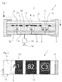
- In der Zeichnung ist ein erfindungsgemäßes Ausführungsbeispiel einer kapazitiven Schaltvorrichtung dargestellt, die nachfolgend näher erläutert ist. Im Einzelnen zeigt:
- Figur 1
- eine kapazitive Schaltvorrichtung mit einem Gehäuse, in dem eine Abdeckplatte aus Glas angeordnet ist und mit einer im Inneren des Gehäuses vorgesehenen Leiterplatte, auf der Sensorflächen zur Erzeugung eines Kapazitätsfeldes, das die in Richtung der Abdeckplatte ausgestrahlt ist, angeordnet sind sowie mit einem zwischen der Abdeckplatte und der Sensorfläche vorgesehenen Reflexionsschirm, im Schnitt und
- Figur 2
- die kapazitive Schaltvorrichtung gemäß
Figur 1 , in Draufsicht mit den auf dem Reflexionsschirm vorhandenen Schaltsymbolen, die durch eine Vielzahl von lichtundurchlässigen Absorptionsschichten gebildet sind. - Aus
Figur 1 und 2 ist eine kapazitive Schaltvorrichtung 1 abgebildet, die aus einem Gehäuse 3 und einer fest an dieser angebrachten Abdeckplatte 4 besteht. Die Abdeckplatte 4 dient als Begrenzung für die im Inneren des Gehäuses 3 angeordneten elektrischen Bauteile, nämlich die auf einer Leiterplatte 7 angebrachten Sensorflächen 6, die aus einem elektrisch leitfähigen Werkstoff gebildet sind. Ein Benutzer erkennt die in der Abdeckplatte 4 integrierten Schaltflächen 5, die fluchtend zu den Sensorflächen 6 angeordnet sind, wenn der Benutzer im Wesentlichen senkrecht auf die Abdeckplatte 4 blickt. Die Bedien- und Blickrichtung ist schematisch mit einem Pfeil wiedergegeben und mit der Bezugsziffer 2 gekennzeichnet. - Die jeweiligen Sensorflächen 6 sind über die Leiterplatte 7 elektrisch mit einer Spannungsquelle 14 gekoppelt und werden von dieser bestromt, so dass die jeweilige Sensorfläche 6 ein Kapazitätsfeld, das die im Wesentlichen in Richtung der Abdeckplatte 4 gerichtet ist, ausstrahlt.
- Darüber hinaus sind der jeweiligen Schaltfläche 5 ein oder mehrere Beleuchtungsmittel 8 zugeordnet, die mit der Stromquelle 14 elektrisch verbunden sind und von dieser im Bedarfsfalle bestromt werden. Die Beleuchtungsmittel 8 sind als sogenannte LEDs ausgestaltet und können unterschiedliche Farbtöne wiedergeben. Die von den Beleuchtungsmitteln 8 abgestrahlten Lichtwellen sind in Richtung der Abdeckplatte 4 gerichtet und durchlaufen die jeweilige Schaltfläche 5, um diese auszuleuchten.
- Zwischen den Beleuchtungsmitteln 8 von zwei zueinander benachbart angeordneter Schaltflächen 5 können lichtdichte Abstandshalter 18 angeordnet sein. Die Abstandshalter 18 bilden für jede Schaltfläche 5 eine Art lichtdichten Hohlraum in dem sich die Beleuchtungsmittel 8 befinden. Somit ist sichergestellt, dass bei der Betätigung der jeweiligen Beleuchtungsmittel 8 nur die zugeordnete Schaltfläche 8 für den Anwender wahrnehmbar ist und die Lichtwellen 10 ausschließlich in Richtung der Abdeckplatte 4 aus diesem Hohlraum austreten können.
- Um einen metallischen visuellen optischen Effekt zu erzeugen, ist im Strahlengang der Lichtwellen 9 der Beleuchtungsmittel 8 ein dünnwandiger Reflexionsschirm 11 angeordnet. Der Reflexionsschirm 11 kann dabei in der Abdeckplatte 4 integriert sein, auf der deren dem Inneren des Gehäuses 3 zugewandten Unterseite oder frei schwebend zwischen der Abdeckplatte 4 und dem Beleuchtungsmitteln 8 angeordnet sein. Der Reflexionsschirm 11 besteht aus einer äußerst dünnwandigen metallischen Struktur, die einen hohen Flächenwiderstand von mehr als 10 3 Ohm/Square aufweist. Somit beeinflusst der Reflexionsschirm 11 die Kapazitäten der Sensorfläche 6 lediglich unwesentlich, so dass die technische Funktionsweise der Sensorfläche 6 weiter besteht.
- Zudem weist der Reflexionsschirm 11 die optische Eigenschaft auf, dass die von den Beleuchtungsmitteln 8 ausgestrahlten Lichtwellen 9 durch diesen an definierten Stellen hindurchtreten können und an z.B. mit einer lichtundurchlässigen Absorptionsschicht 12 nach Art eines Sperrdrucks, versehenen Stellen, blockiert werden. Die von außen auf den Reflexionsschirm 11 auftreffenden Lichtwellen werden von dem Reflexionsschirm 11 teilweise reflektiert, gebrochen und/oder gestreut. Somit entsteht durch die Reflexion Streuung und/oder Brechung der äußeren Lichtwellen der optische Eindruck, dass die verwendeten Reflexionsschirme eine metallische glänzende Ästhetik aufweisen. Im ausgeschalteten Zustand erscheint die Oberfläche als durchgehend homogene metallene Fläche.
- Darüber hinaus kann die Schaltvorrichtung 1 als eine Art Display 15 verwendet werden, wenn nämlich auf der Ober- und/oder Unterseite des Reflexionsschirmes lichtundurchlässige Absorptionsschichten 12 aufgetragen, aufgedruckt oder aufgeklebt sind. Die lichtundurchlässigen Absorptionsschichten 12 können Aussparungen 13 aufweisen, die lichtdurchlässig sind, so dass die Konturen der lichtundurchlässigen Absorptionsschichten 12 zu einem Schaltsymbol in Form von Zahlen, Buchstaben oder dergleichen ausgestaltet sind. Es ist ohne weiteres möglich die lichtundurchlässigen Absorptionsschichten 12 über die gesamte Oberfläche oder Unterseite der Reflexionsschirme 11 aufzutragen und die Aussparungen 12 mit den Lichtwellen der Beleuchtungsmittel 8 auszuleuchten.
- Ebenso kann an der Stelle der Beleuchtungsmittel 8 ein oder mehrere herkömmliche Flachbildschirme oder Anzeigegeräte z.B. ein TFT- oder LC- Display 15 hinter den Reflexionsschirm 11 platziert werden, die in dem Betrieb durchscheinen, ausgeschalten jedoch nicht sichtbar sind und die Oberfläche homogen metallen erscheint. Die Lichtwellen 10 der Beleuchtungsmittel 8 können ebenfalls mittels Lichtleitern oder anderen optischen Bauteilen zu der jeweiligen Schaltflächen 5 gelenkt werden.
Claims (11)
- Kapazitive Schaltvorrichtung (1) zur Erzeugung mindestens eines elektrisch auswertbaren Schaltsignals, durch das ein elektrisches Gerät, beispielsweise ein Telefon, eine Werkzeugmaschine, ein Kühlschrank oder dergleichen manuell bedienbar ist,- mit einer in einem Gehäuse (3) angeordneten Abdeckplatte (4), die aus einem transparenten oder semitransparenten Werkstoff, insbesondere aus Glas oder aus einem Kunststoff, hergestellt ist, und durch die mindestens eine Schaltfläche (5) erkennbar und von außen bedienbar ist,- mit mindestens einer ein Kapazitätsfeld erzeugende Sensorfläche (6), die aus einem elektrisch leitfähigen Werkstoff hergestellt und die auf eine im Inneren des Gehäuses (3) an vorgesehenen Träger- oder Leiterplatten (7) aufgebracht ist und die fluchtend zu der jeweiligen Schaltfläche (5) ausgerichtet ist,- mit mindestens einem in dem Gehäuse (3) angebrachten Beleuchtungsmittel (8), insbesondere einer LED, durch die Lichtwellen (10), die in einem auf die Abdeckplatte (4) gerichteten Strahlengang (9) verlaufen, erzeugt sind und durch die die jeweilige Schaltfläche (5) beleuchtet ist und- mit einer Spannungsquelle (14) zur Bestromung der Sensorfläche und den Beleuchtungsmitteln,dadurch gekennzeichnet,
dass im Strahlengang (9) der jeweiligen Lichtwelle (10) der Beleuchtungsmittel (8) ein dünnwandiger Reflexionsschirm (11) angeordnet ist, dass die von den Beleuchtungsmitteln (8) in Richtung des Reflexionsschirmes (11) abgestrahlten Lichtwellen (10) durch diesen nach außen hindurchlaufen und dass die von außen auf den Reflexionsschirm (11) einfallenden Lichtwellen von diesen teilweise reflektiert, gebrochen und/oder gestreut sind. - Schaltvorrichtung nach Anspruch 1,
dadurch gekennzeichnet,
dass auf der Ober- und/oder Unterseite des Reflexionsschirmes (11) eine lichtundurchlässige Absorptionsschicht (12) aufgebracht ist, dass die lichtundurchlässige Absorptionsschicht (12) ein oder mehrerer lichtdurchlässige Aussparungen (13) aufweist, dass die Aussparungen (13) ein Steuersymbol, beispielsweise in Form von Zahlen, Buchstaben oder dergleichen bilden oder vice versa. - Schaltvorrichtung nach Anspruch 1 oder 2,
dadurch gekennzeichnet,
dass der Reflexionsschirm (11) als Flächengebilde mit einer planen, gekrümmten oder gewellten Außenkontur ausgestaltet ist, die senkrecht zu dem Strahlengang (9) der Lichtwellen (10) verläuft, und dass durch die Wandstärke des Reflexionsschirmes (11) das von der Sensorfläche (6) abgestrahlte Kapazitätsfeld ungehindert oder nahezu ohne Abschirmeffekte durch diesen gelangt. - Schaltvorrichtung nach einem der vorgenannten Ansprüche,
dadurch gekennzeichnet,
dass sich die flächige Abmessung des Reflexionsschirmes (11) an die Abdeckplatte (4) angepasst ist und sich durchgängig über deren gesamte Fläche erstreckt. - Schaltvorrichtung nach einem der vorgenannten Ansprüche,
dadurch gekennzeichnet,
dass der Reflexionsschirm (11) folienartig auf die Unterseite der Abdeckplatte (4) aufgebracht oder aufgetragen ist, oder dass der Reflexionsschirm (11) beabstandet zu der Abdeckplatte (4) verläuft und durch das Gehäuse (3) lageorientiert gehalten ist. - Schaltvorrichtung nach einem der vorgenannten Ansprüche,
dass der Reflexionsschirm (11) aus einem elektrisch leitenden Werkstoff, vorzugsweise aus Metall hergestellt ist. - Schaltvorrichtung nach einem der vorgenannten Ansprüche,
dadurch gekennzeichnet,
dass der Werkstoff des Reflexionsschirmes (11) einen Flächenwiderstand größer als 103 Ohm/square aufweist. - Schaltvorrichtung nach einem der vorgenannten Ansprüche,
dadurch gekennzeichnet,
dass zwischen den Beleuchtungsmittel (8) zweier benachbarter Schaltflächen (5) ein Abstandshalter (18) angeordnet ist, und dass der Abstandshalter (18) die benachbarten Schaltflächen (5) lichtdicht trennt. - Schaltvorrichtung nach einem der vorgenannten Ansprüche
dadurch gekennzeichnet,
dass die jeweilige Sensorfläche (6) lichtundurchlässig oder lichtreflektierend ausgestaltet ist und dass diese mit einem IC-Schaltkreis einer Steuer- und Auswerteeinrichtung (16) elektrisch gekoppelt ist, durch die die Veränderungen des von der jeweiligen Sensorfläche (6) erzeugten Kapazitätsfeldes (2) im Bereich der Schaltfläche (5) in X- und/oder Y-Richtung bezogen auf das X-Y-Koordinatensystem (17) der Schaltfläche (5) erfassbar sind. - Schaltvorrichtung nach Anspruch 9,
dadurch gekennzeichnet,
dass durch die elektrische Steuer- und Auswertevorrichtung (16), vorzugsweise einen Mikrocontroller, Mikroprozessor oder einen integrierten Schaltkreis, die jeweiligen Beleuchtungsmittel (8) elektrisch verbunden sind und dass in Abhängigkeit von der gemessenen bzw. erfassten Kapazitätsfeldveränderungen (2) auf der Schaltfläche (5) der Abdeckplatte (4) die Beleuchtungsmittel (8) durch die elektrische Steuereinrichtung (16) derart geschaltet sind, dass die Farbe der Lichtwellen (10) veränderbar ist oder dass die Beleuchtungsmittel (8) aus- bzw. eingeschaltet sind. - Schaltvorrichtung nach einem der vorgenannten Ansprüche,
dadurch gekennzeichnet,
dass in dem Strahlengang (9) der Lichtwellen (10) und räumlich vor dem Reflexionsschirm (11) ein Anzeigegerät, vorzugsweise ein TFT- oder LC-Display (15), angeordnet ist
Priority Applications (2)
| Application Number | Priority Date | Filing Date | Title |
|---|---|---|---|
| EP15188750.2A EP3154200B1 (de) | 2015-10-07 | 2015-10-07 | Kapazitive schaltvorrichtung |
| PL15188750T PL3154200T3 (pl) | 2015-10-07 | 2015-10-07 | Przełącznik pojemnościowy |
Applications Claiming Priority (1)
| Application Number | Priority Date | Filing Date | Title |
|---|---|---|---|
| EP15188750.2A EP3154200B1 (de) | 2015-10-07 | 2015-10-07 | Kapazitive schaltvorrichtung |
Publications (2)
| Publication Number | Publication Date |
|---|---|
| EP3154200A1 true EP3154200A1 (de) | 2017-04-12 |
| EP3154200B1 EP3154200B1 (de) | 2020-12-23 |
Family
ID=54288676
Family Applications (1)
| Application Number | Title | Priority Date | Filing Date |
|---|---|---|---|
| EP15188750.2A Active EP3154200B1 (de) | 2015-10-07 | 2015-10-07 | Kapazitive schaltvorrichtung |
Country Status (2)
| Country | Link |
|---|---|
| EP (1) | EP3154200B1 (de) |
| PL (1) | PL3154200T3 (de) |
Cited By (2)
| Publication number | Priority date | Publication date | Assignee | Title |
|---|---|---|---|---|
| EP3594792A1 (de) * | 2018-07-13 | 2020-01-15 | Vestel Beyaz Esya Sanayi Ve Ticaret A.S. | Berührungssteuerungssystem |
| DE102024120882A1 (de) | 2024-07-23 | 2026-01-29 | E.G.O. Elektro-Gerätebau GmbH | Anzeigevorrichtung für ein Elektrogerät, Elektrogerät mit einer solchen Anzeigevorrichtung und Verfahren zur Herstellung einer Anzeigevorrichtung |
Citations (7)
| Publication number | Priority date | Publication date | Assignee | Title |
|---|---|---|---|---|
| US6958459B2 (en) * | 2003-05-07 | 2005-10-25 | Schott Ag | Contact switching arrangement |
| EP1688308A2 (de) * | 2005-02-04 | 2006-08-09 | Adac Plastics, Inc. | Verkleidungsteil mit versteckter Beschriftung |
| WO2009036552A1 (en) * | 2007-09-17 | 2009-03-26 | Magna International Inc. | Touchless keyless entry keypad integrated with electroluminescence backlight |
| US20100219935A1 (en) * | 2004-10-26 | 2010-09-02 | Adac Plastics, Inc. | Keyless entry system incorporating concealable keypad |
| EP2385630A2 (de) * | 2010-05-04 | 2011-11-09 | Whirlpool Corporation | Berührungsaktivierte Benutzerschnittstelle |
| EP2611034A2 (de) * | 2011-12-26 | 2013-07-03 | Kabushiki Kaisha Toshiba | Elektronische Vorrichtung |
| EP2645571A1 (de) | 2012-03-27 | 2013-10-02 | RAFI GmbH & Co. KG | Kapazitive Schaltvorrichtung |
-
2015
- 2015-10-07 PL PL15188750T patent/PL3154200T3/pl unknown
- 2015-10-07 EP EP15188750.2A patent/EP3154200B1/de active Active
Patent Citations (7)
| Publication number | Priority date | Publication date | Assignee | Title |
|---|---|---|---|---|
| US6958459B2 (en) * | 2003-05-07 | 2005-10-25 | Schott Ag | Contact switching arrangement |
| US20100219935A1 (en) * | 2004-10-26 | 2010-09-02 | Adac Plastics, Inc. | Keyless entry system incorporating concealable keypad |
| EP1688308A2 (de) * | 2005-02-04 | 2006-08-09 | Adac Plastics, Inc. | Verkleidungsteil mit versteckter Beschriftung |
| WO2009036552A1 (en) * | 2007-09-17 | 2009-03-26 | Magna International Inc. | Touchless keyless entry keypad integrated with electroluminescence backlight |
| EP2385630A2 (de) * | 2010-05-04 | 2011-11-09 | Whirlpool Corporation | Berührungsaktivierte Benutzerschnittstelle |
| EP2611034A2 (de) * | 2011-12-26 | 2013-07-03 | Kabushiki Kaisha Toshiba | Elektronische Vorrichtung |
| EP2645571A1 (de) | 2012-03-27 | 2013-10-02 | RAFI GmbH & Co. KG | Kapazitive Schaltvorrichtung |
Cited By (2)
| Publication number | Priority date | Publication date | Assignee | Title |
|---|---|---|---|---|
| EP3594792A1 (de) * | 2018-07-13 | 2020-01-15 | Vestel Beyaz Esya Sanayi Ve Ticaret A.S. | Berührungssteuerungssystem |
| DE102024120882A1 (de) | 2024-07-23 | 2026-01-29 | E.G.O. Elektro-Gerätebau GmbH | Anzeigevorrichtung für ein Elektrogerät, Elektrogerät mit einer solchen Anzeigevorrichtung und Verfahren zur Herstellung einer Anzeigevorrichtung |
Also Published As
| Publication number | Publication date |
|---|---|
| PL3154200T3 (pl) | 2021-06-14 |
| EP3154200B1 (de) | 2020-12-23 |
Similar Documents
| Publication | Publication Date | Title |
|---|---|---|
| EP1257057B1 (de) | Sensorelement für einen kapazitiven Berührungsschalter | |
| EP3280053B1 (de) | Bedienmodul für ein haushaltsgerät | |
| DE102011077896A1 (de) | Bedien- und Anzeigeeinrichtung für ein Haushaltsgerät und Haushaltsgerät | |
| DE102018110033B3 (de) | Eingabegerät mit einem Array von Kraftsensoren im Folienschichtaufbau mit verbesserter Haltbarkeit und vereinfachter Herstellung | |
| DE60219369T2 (de) | Tastenfeld für verkaufsmaschinen | |
| DE102011081331A1 (de) | Haushaltsgerät mit einer berührungssensitiven Bedien- und Anzeigeeinrichtung | |
| WO2012175336A2 (de) | Kapazitive bedien- und anzeigeeinrichtung für ein haushaltsgerät und haushaltsgerät mit einer solchen bedien- und anzeigeeinrichtung | |
| EP2085702A2 (de) | Hausgerät mit einer Markierung und mit einer Beleuchtungsanordnung | |
| DE102016123118A1 (de) | Eingabegerät mit einem Array von Kraftsensoren im Folienschichtaufbau mit verbesserter Hinterleuchtung | |
| EP3520218B1 (de) | Schichtenverbund zur bereitstellung eines bedienelements für ein hausgerät | |
| EP1903284B1 (de) | Vorrichtung für ein Haushaltsgerät und Verwendung der Vorrichtung | |
| DE10259297A1 (de) | Beleuchtungseinrichtung für Schaltflächen | |
| DE10320548B4 (de) | Berührungsschalteinrichtung | |
| EP2830220A1 (de) | Bedienteil für eine Bedieneinrichtung und Bedieneinrichtung | |
| EP3154200A1 (de) | Kapazitive schaltvorrichtung | |
| EP2748368B1 (de) | Haushaltsgerät mit einer berührungssensitiven bedien- und anzeigeeinrichtung | |
| DE102005027192A1 (de) | Sensorelementvorrichtung für eine Bedieneinrichtung eines Kochfeldes und Anordnung eines Kochfeldes in einer Arbeitsplatte | |
| DE102014019439B4 (de) | Verkleidungsvorrichtung für ein Kraftfahrzeug und Kraftfahrzeug | |
| EP2645571A1 (de) | Kapazitive Schaltvorrichtung | |
| EP3369179A1 (de) | Kapazitiver berührungsschalter | |
| DE102013000365B4 (de) | Bedienelement für einen Kraftwagen und Kraftwagen | |
| DE102015016293A1 (de) | Anzeigevorrichtung, insbesondere für eine Bedienvorrichtung | |
| DE102021209964B3 (de) | Bedieneinrichtung für ein Elektrogerät und Elektrogerät mit einer solchen Bedieneinrichtung | |
| EP3579415A1 (de) | Verfahren zur bedienung eines elektrokochgeräts und elektrokochgerät | |
| EP3200349A1 (de) | Kapazitive benutzerschnittstelle |
Legal Events
| Date | Code | Title | Description |
|---|---|---|---|
| PUAI | Public reference made under article 153(3) epc to a published international application that has entered the european phase |
Free format text: ORIGINAL CODE: 0009012 |
|
| STAA | Information on the status of an ep patent application or granted ep patent |
Free format text: STATUS: THE APPLICATION HAS BEEN PUBLISHED |
|
| AK | Designated contracting states |
Kind code of ref document: A1 Designated state(s): AL AT BE BG CH CY CZ DE DK EE ES FI FR GB GR HR HU IE IS IT LI LT LU LV MC MK MT NL NO PL PT RO RS SE SI SK SM TR |
|
| AX | Request for extension of the european patent |
Extension state: BA ME |
|
| STAA | Information on the status of an ep patent application or granted ep patent |
Free format text: STATUS: REQUEST FOR EXAMINATION WAS MADE |
|
| 17P | Request for examination filed |
Effective date: 20171010 |
|
| RBV | Designated contracting states (corrected) |
Designated state(s): AL AT BE BG CH CY CZ DE DK EE ES FI FR GB GR HR HU IE IS IT LI LT LU LV MC MK MT NL NO PL PT RO RS SE SI SK SM TR |
|
| GRAP | Despatch of communication of intention to grant a patent |
Free format text: ORIGINAL CODE: EPIDOSNIGR1 |
|
| STAA | Information on the status of an ep patent application or granted ep patent |
Free format text: STATUS: GRANT OF PATENT IS INTENDED |
|
| INTG | Intention to grant announced |
Effective date: 20200924 |
|
| GRAS | Grant fee paid |
Free format text: ORIGINAL CODE: EPIDOSNIGR3 |
|
| GRAA | (expected) grant |
Free format text: ORIGINAL CODE: 0009210 |
|
| STAA | Information on the status of an ep patent application or granted ep patent |
Free format text: STATUS: THE PATENT HAS BEEN GRANTED |
|
| AK | Designated contracting states |
Kind code of ref document: B1 Designated state(s): AL AT BE BG CH CY CZ DE DK EE ES FI FR GB GR HR HU IE IS IT LI LT LU LV MC MK MT NL NO PL PT RO RS SE SI SK SM TR |
|
| REG | Reference to a national code |
Ref country code: GB Ref legal event code: FG4D Free format text: NOT ENGLISH |
|
| REG | Reference to a national code |
Ref country code: DE Ref legal event code: R096 Ref document number: 502015014036 Country of ref document: DE |
|
| REG | Reference to a national code |
Ref country code: AT Ref legal event code: REF Ref document number: 1348712 Country of ref document: AT Kind code of ref document: T Effective date: 20210115 |
|
| REG | Reference to a national code |
Ref country code: IE Ref legal event code: FG4D Free format text: LANGUAGE OF EP DOCUMENT: GERMAN |
|
| PG25 | Lapsed in a contracting state [announced via postgrant information from national office to epo] |
Ref country code: RS Free format text: LAPSE BECAUSE OF FAILURE TO SUBMIT A TRANSLATION OF THE DESCRIPTION OR TO PAY THE FEE WITHIN THE PRESCRIBED TIME-LIMIT Effective date: 20201223 Ref country code: FI Free format text: LAPSE BECAUSE OF FAILURE TO SUBMIT A TRANSLATION OF THE DESCRIPTION OR TO PAY THE FEE WITHIN THE PRESCRIBED TIME-LIMIT Effective date: 20201223 Ref country code: NO Free format text: LAPSE BECAUSE OF FAILURE TO SUBMIT A TRANSLATION OF THE DESCRIPTION OR TO PAY THE FEE WITHIN THE PRESCRIBED TIME-LIMIT Effective date: 20210323 Ref country code: GR Free format text: LAPSE BECAUSE OF FAILURE TO SUBMIT A TRANSLATION OF THE DESCRIPTION OR TO PAY THE FEE WITHIN THE PRESCRIBED TIME-LIMIT Effective date: 20210324 |
|
| REG | Reference to a national code |
Ref country code: NL Ref legal event code: MP Effective date: 20201223 |
|
| PG25 | Lapsed in a contracting state [announced via postgrant information from national office to epo] |
Ref country code: BG Free format text: LAPSE BECAUSE OF FAILURE TO SUBMIT A TRANSLATION OF THE DESCRIPTION OR TO PAY THE FEE WITHIN THE PRESCRIBED TIME-LIMIT Effective date: 20210323 Ref country code: SE Free format text: LAPSE BECAUSE OF FAILURE TO SUBMIT A TRANSLATION OF THE DESCRIPTION OR TO PAY THE FEE WITHIN THE PRESCRIBED TIME-LIMIT Effective date: 20201223 Ref country code: LV Free format text: LAPSE BECAUSE OF FAILURE TO SUBMIT A TRANSLATION OF THE DESCRIPTION OR TO PAY THE FEE WITHIN THE PRESCRIBED TIME-LIMIT Effective date: 20201223 |
|
| PG25 | Lapsed in a contracting state [announced via postgrant information from national office to epo] |
Ref country code: NL Free format text: LAPSE BECAUSE OF FAILURE TO SUBMIT A TRANSLATION OF THE DESCRIPTION OR TO PAY THE FEE WITHIN THE PRESCRIBED TIME-LIMIT Effective date: 20201223 Ref country code: HR Free format text: LAPSE BECAUSE OF FAILURE TO SUBMIT A TRANSLATION OF THE DESCRIPTION OR TO PAY THE FEE WITHIN THE PRESCRIBED TIME-LIMIT Effective date: 20201223 |
|
| REG | Reference to a national code |
Ref country code: LT Ref legal event code: MG9D |
|
| PG25 | Lapsed in a contracting state [announced via postgrant information from national office to epo] |
Ref country code: EE Free format text: LAPSE BECAUSE OF FAILURE TO SUBMIT A TRANSLATION OF THE DESCRIPTION OR TO PAY THE FEE WITHIN THE PRESCRIBED TIME-LIMIT Effective date: 20201223 Ref country code: CZ Free format text: LAPSE BECAUSE OF FAILURE TO SUBMIT A TRANSLATION OF THE DESCRIPTION OR TO PAY THE FEE WITHIN THE PRESCRIBED TIME-LIMIT Effective date: 20201223 Ref country code: SM Free format text: LAPSE BECAUSE OF FAILURE TO SUBMIT A TRANSLATION OF THE DESCRIPTION OR TO PAY THE FEE WITHIN THE PRESCRIBED TIME-LIMIT Effective date: 20201223 Ref country code: LT Free format text: LAPSE BECAUSE OF FAILURE TO SUBMIT A TRANSLATION OF THE DESCRIPTION OR TO PAY THE FEE WITHIN THE PRESCRIBED TIME-LIMIT Effective date: 20201223 Ref country code: RO Free format text: LAPSE BECAUSE OF FAILURE TO SUBMIT A TRANSLATION OF THE DESCRIPTION OR TO PAY THE FEE WITHIN THE PRESCRIBED TIME-LIMIT Effective date: 20201223 Ref country code: PT Free format text: LAPSE BECAUSE OF FAILURE TO SUBMIT A TRANSLATION OF THE DESCRIPTION OR TO PAY THE FEE WITHIN THE PRESCRIBED TIME-LIMIT Effective date: 20210423 Ref country code: SK Free format text: LAPSE BECAUSE OF FAILURE TO SUBMIT A TRANSLATION OF THE DESCRIPTION OR TO PAY THE FEE WITHIN THE PRESCRIBED TIME-LIMIT Effective date: 20201223 |
|
| REG | Reference to a national code |
Ref country code: DE Ref legal event code: R097 Ref document number: 502015014036 Country of ref document: DE |
|
| PG25 | Lapsed in a contracting state [announced via postgrant information from national office to epo] |
Ref country code: IS Free format text: LAPSE BECAUSE OF FAILURE TO SUBMIT A TRANSLATION OF THE DESCRIPTION OR TO PAY THE FEE WITHIN THE PRESCRIBED TIME-LIMIT Effective date: 20210423 |
|
| PG25 | Lapsed in a contracting state [announced via postgrant information from national office to epo] |
Ref country code: AL Free format text: LAPSE BECAUSE OF FAILURE TO SUBMIT A TRANSLATION OF THE DESCRIPTION OR TO PAY THE FEE WITHIN THE PRESCRIBED TIME-LIMIT Effective date: 20201223 |
|
| PLBE | No opposition filed within time limit |
Free format text: ORIGINAL CODE: 0009261 |
|
| STAA | Information on the status of an ep patent application or granted ep patent |
Free format text: STATUS: NO OPPOSITION FILED WITHIN TIME LIMIT |
|
| PG25 | Lapsed in a contracting state [announced via postgrant information from national office to epo] |
Ref country code: ES Free format text: LAPSE BECAUSE OF FAILURE TO SUBMIT A TRANSLATION OF THE DESCRIPTION OR TO PAY THE FEE WITHIN THE PRESCRIBED TIME-LIMIT Effective date: 20201223 Ref country code: DK Free format text: LAPSE BECAUSE OF FAILURE TO SUBMIT A TRANSLATION OF THE DESCRIPTION OR TO PAY THE FEE WITHIN THE PRESCRIBED TIME-LIMIT Effective date: 20201223 |
|
| 26N | No opposition filed |
Effective date: 20210924 |
|
| PG25 | Lapsed in a contracting state [announced via postgrant information from national office to epo] |
Ref country code: SI Free format text: LAPSE BECAUSE OF FAILURE TO SUBMIT A TRANSLATION OF THE DESCRIPTION OR TO PAY THE FEE WITHIN THE PRESCRIBED TIME-LIMIT Effective date: 20201223 |
|
| REG | Reference to a national code |
Ref country code: DE Ref legal event code: R082 Ref document number: 502015014036 Country of ref document: DE Representative=s name: GEITZ PATENTANWAELTE PARTG MBB, DE Ref country code: DE Ref legal event code: R082 Ref document number: 502015014036 Country of ref document: DE Representative=s name: GEITZ TRUCKENMUELLER LUCHT CHRIST PATENTANWAEL, DE |
|
| PG25 | Lapsed in a contracting state [announced via postgrant information from national office to epo] |
Ref country code: IS Free format text: LAPSE BECAUSE OF FAILURE TO SUBMIT A TRANSLATION OF THE DESCRIPTION OR TO PAY THE FEE WITHIN THE PRESCRIBED TIME-LIMIT Effective date: 20210423 |
|
| REG | Reference to a national code |
Ref country code: BE Ref legal event code: MM Effective date: 20211031 |
|
| PG25 | Lapsed in a contracting state [announced via postgrant information from national office to epo] |
Ref country code: MC Free format text: LAPSE BECAUSE OF FAILURE TO SUBMIT A TRANSLATION OF THE DESCRIPTION OR TO PAY THE FEE WITHIN THE PRESCRIBED TIME-LIMIT Effective date: 20201223 |
|
| PG25 | Lapsed in a contracting state [announced via postgrant information from national office to epo] |
Ref country code: LU Free format text: LAPSE BECAUSE OF NON-PAYMENT OF DUE FEES Effective date: 20211007 Ref country code: BE Free format text: LAPSE BECAUSE OF NON-PAYMENT OF DUE FEES Effective date: 20211031 |
|
| PG25 | Lapsed in a contracting state [announced via postgrant information from national office to epo] |
Ref country code: IE Free format text: LAPSE BECAUSE OF NON-PAYMENT OF DUE FEES Effective date: 20211007 |
|
| PG25 | Lapsed in a contracting state [announced via postgrant information from national office to epo] |
Ref country code: HU Free format text: LAPSE BECAUSE OF FAILURE TO SUBMIT A TRANSLATION OF THE DESCRIPTION OR TO PAY THE FEE WITHIN THE PRESCRIBED TIME-LIMIT; INVALID AB INITIO Effective date: 20151007 |
|
| P01 | Opt-out of the competence of the unified patent court (upc) registered |
Effective date: 20230513 |
|
| PG25 | Lapsed in a contracting state [announced via postgrant information from national office to epo] |
Ref country code: CY Free format text: LAPSE BECAUSE OF FAILURE TO SUBMIT A TRANSLATION OF THE DESCRIPTION OR TO PAY THE FEE WITHIN THE PRESCRIBED TIME-LIMIT Effective date: 20201223 |
|
| PG25 | Lapsed in a contracting state [announced via postgrant information from national office to epo] |
Ref country code: MK Free format text: LAPSE BECAUSE OF FAILURE TO SUBMIT A TRANSLATION OF THE DESCRIPTION OR TO PAY THE FEE WITHIN THE PRESCRIBED TIME-LIMIT Effective date: 20201223 |
|
| PG25 | Lapsed in a contracting state [announced via postgrant information from national office to epo] |
Ref country code: MT Free format text: LAPSE BECAUSE OF FAILURE TO SUBMIT A TRANSLATION OF THE DESCRIPTION OR TO PAY THE FEE WITHIN THE PRESCRIBED TIME-LIMIT Effective date: 20201223 |
|
| PGFP | Annual fee paid to national office [announced via postgrant information from national office to epo] |
Ref country code: PL Payment date: 20250930 Year of fee payment: 11 |
|
| REG | Reference to a national code |
Ref country code: CH Ref legal event code: U11 Free format text: ST27 STATUS EVENT CODE: U-0-0-U10-U11 (AS PROVIDED BY THE NATIONAL OFFICE) Effective date: 20251101 |
|
| PG25 | Lapsed in a contracting state [announced via postgrant information from national office to epo] |
Ref country code: TR Free format text: LAPSE BECAUSE OF FAILURE TO SUBMIT A TRANSLATION OF THE DESCRIPTION OR TO PAY THE FEE WITHIN THE PRESCRIBED TIME-LIMIT Effective date: 20201223 |
|
| PGFP | Annual fee paid to national office [announced via postgrant information from national office to epo] |
Ref country code: DE Payment date: 20251020 Year of fee payment: 11 |
|
| PGFP | Annual fee paid to national office [announced via postgrant information from national office to epo] |
Ref country code: GB Payment date: 20251024 Year of fee payment: 11 |
|
| PGFP | Annual fee paid to national office [announced via postgrant information from national office to epo] |
Ref country code: AT Payment date: 20251021 Year of fee payment: 11 |
|
| PGFP | Annual fee paid to national office [announced via postgrant information from national office to epo] |
Ref country code: IT Payment date: 20251031 Year of fee payment: 11 |
|
| PGFP | Annual fee paid to national office [announced via postgrant information from national office to epo] |
Ref country code: FR Payment date: 20251027 Year of fee payment: 11 |
|
| PGFP | Annual fee paid to national office [announced via postgrant information from national office to epo] |
Ref country code: CH Payment date: 20251101 Year of fee payment: 11 |