EP3148073A1 - Apparatus for performing capacitor amplification in an electronic device - Google Patents
Apparatus for performing capacitor amplification in an electronic device Download PDFInfo
- Publication number
- EP3148073A1 EP3148073A1 EP16170308.7A EP16170308A EP3148073A1 EP 3148073 A1 EP3148073 A1 EP 3148073A1 EP 16170308 A EP16170308 A EP 16170308A EP 3148073 A1 EP3148073 A1 EP 3148073A1
- Authority
- EP
- European Patent Office
- Prior art keywords
- terminal
- coupled
- common mode
- capacitor
- mosfet
- Prior art date
- Legal status (The legal status is an assumption and is not a legal conclusion. Google has not performed a legal analysis and makes no representation as to the accuracy of the status listed.)
- Withdrawn
Links
- 239000003990 capacitor Substances 0.000 title claims abstract description 81
- 230000003321 amplification Effects 0.000 title claims abstract description 33
- 238000003199 nucleic acid amplification method Methods 0.000 title claims abstract description 33
- 238000010168 coupling process Methods 0.000 claims description 11
- 238000005859 coupling reaction Methods 0.000 claims description 11
- 230000008878 coupling Effects 0.000 claims description 4
- 230000005669 field effect Effects 0.000 claims description 2
- 229910044991 metal oxide Inorganic materials 0.000 claims description 2
- 150000004706 metal oxides Chemical class 0.000 claims description 2
- 239000004065 semiconductor Substances 0.000 claims description 2
- 238000010586 diagram Methods 0.000 description 2
- 238000000034 method Methods 0.000 description 2
- 230000004075 alteration Effects 0.000 description 1
- 230000008901 benefit Effects 0.000 description 1
- 238000007796 conventional method Methods 0.000 description 1
- 230000003247 decreasing effect Effects 0.000 description 1
- 230000000593 degrading effect Effects 0.000 description 1
- 238000013461 design Methods 0.000 description 1
- 230000000694 effects Effects 0.000 description 1
- 238000012986 modification Methods 0.000 description 1
- 230000004048 modification Effects 0.000 description 1
- 230000008569 process Effects 0.000 description 1
Images

Classifications
-
- H—ELECTRICITY
- H03—ELECTRONIC CIRCUITRY
- H03F—AMPLIFIERS
- H03F3/00—Amplifiers with only discharge tubes or only semiconductor devices as amplifying elements
- H03F3/45—Differential amplifiers
- H03F3/45071—Differential amplifiers with semiconductor devices only
- H03F3/45076—Differential amplifiers with semiconductor devices only characterised by the way of implementation of the active amplifying circuit in the differential amplifier
- H03F3/45179—Differential amplifiers with semiconductor devices only characterised by the way of implementation of the active amplifying circuit in the differential amplifier using MOSFET transistors as the active amplifying circuit
-
- H—ELECTRICITY
- H03—ELECTRONIC CIRCUITRY
- H03F—AMPLIFIERS
- H03F3/00—Amplifiers with only discharge tubes or only semiconductor devices as amplifying elements
- H03F3/50—Amplifiers in which input is applied to, or output is derived from, an impedance common to input and output circuits of the amplifying element, e.g. cathode follower
- H03F3/505—Amplifiers in which input is applied to, or output is derived from, an impedance common to input and output circuits of the amplifying element, e.g. cathode follower with field-effect devices
-
- H—ELECTRICITY
- H03—ELECTRONIC CIRCUITRY
- H03F—AMPLIFIERS
- H03F1/00—Details of amplifiers with only discharge tubes, only semiconductor devices or only unspecified devices as amplifying elements
- H03F1/34—Negative-feedback-circuit arrangements with or without positive feedback
- H03F1/342—Negative-feedback-circuit arrangements with or without positive feedback in field-effect transistor amplifiers
-
- H—ELECTRICITY
- H03—ELECTRONIC CIRCUITRY
- H03F—AMPLIFIERS
- H03F2200/00—Indexing scheme relating to amplifiers
- H03F2200/129—Indexing scheme relating to amplifiers there being a feedback over the complete amplifier
-
- H—ELECTRICITY
- H03—ELECTRONIC CIRCUITRY
- H03F—AMPLIFIERS
- H03F2200/00—Indexing scheme relating to amplifiers
- H03F2200/144—Indexing scheme relating to amplifiers the feedback circuit of the amplifier stage comprising a passive resistor and passive capacitor
-
- H—ELECTRICITY
- H03—ELECTRONIC CIRCUITRY
- H03F—AMPLIFIERS
- H03F2200/00—Indexing scheme relating to amplifiers
- H03F2200/21—Bias resistors are added at the input of an amplifier
-
- H—ELECTRICITY
- H03—ELECTRONIC CIRCUITRY
- H03F—AMPLIFIERS
- H03F2200/00—Indexing scheme relating to amplifiers
- H03F2200/303—Indexing scheme relating to amplifiers the loading circuit of an amplifying stage comprising a diode or diode coupled transistor
-
- H—ELECTRICITY
- H03—ELECTRONIC CIRCUITRY
- H03F—AMPLIFIERS
- H03F2200/00—Indexing scheme relating to amplifiers
- H03F2200/42—Indexing scheme relating to amplifiers the input to the amplifier being made by capacitive coupling means
-
- H—ELECTRICITY
- H03—ELECTRONIC CIRCUITRY
- H03F—AMPLIFIERS
- H03F2200/00—Indexing scheme relating to amplifiers
- H03F2200/69—Indexing scheme relating to amplifiers the amplifier stage being a common drain coupled MOSFET, i.e. source follower
-
- H—ELECTRICITY
- H03—ELECTRONIC CIRCUITRY
- H03F—AMPLIFIERS
- H03F2203/00—Indexing scheme relating to amplifiers with only discharge tubes or only semiconductor devices as amplifying elements covered by H03F3/00
- H03F2203/45—Indexing scheme relating to differential amplifiers
- H03F2203/45061—Indexing scheme relating to differential amplifiers the common mode reference signal being taken or deducted from the one or more inputs of the differential amplifier
-
- H—ELECTRICITY
- H03—ELECTRONIC CIRCUITRY
- H03F—AMPLIFIERS
- H03F2203/00—Indexing scheme relating to amplifiers with only discharge tubes or only semiconductor devices as amplifying elements covered by H03F3/00
- H03F2203/45—Indexing scheme relating to differential amplifiers
- H03F2203/45084—Indexing scheme relating to differential amplifiers the common mode signal circuit comprising one or more inductive or capacitive elements, e.g. filter circuitry
-
- H—ELECTRICITY
- H03—ELECTRONIC CIRCUITRY
- H03F—AMPLIFIERS
- H03F2203/00—Indexing scheme relating to amplifiers with only discharge tubes or only semiconductor devices as amplifying elements covered by H03F3/00
- H03F2203/50—Indexing scheme relating to amplifiers in which input being applied to, or output being derived from, an impedance common to input and output circuits of the amplifying element, e.g. cathode follower
- H03F2203/5024—Indexing scheme relating to amplifiers in which input being applied to, or output being derived from, an impedance common to input and output circuits of the amplifying element, e.g. cathode follower the source follower has a controlled source circuit, the source circuit being controlled via a capacitor, i.e. AC-controlled
Definitions
- the present invention relates to alternating current (AC)-coupled capacitor amplification for common-mode termination, and more particularly, to an apparatus for performing capacitor amplification in an electronic device according to the pre-characterizing clauses of claim 1.
- AC alternating current
- a direct current (DC) coupling system may be designed to have a floating termination architecture, and it looks like open circuit in one or more situations. Based on this design, some problems may occur. For example, a capacitor having a capacitance value of more than one hundred picofarad (pF) may be required, causing the associated chip area to be increased. As a result, the associated costs are increased.
- Some conventional methods are proposed to try solving the problems, but additional problems such as some side effects may occur. For example, a receiver may need a wide input range of bandwidth and may require strong signal driving of an amplifier, causing increased costs and increased power consumption. In another example, a receiver may suffer from a slow operation speed and a large input common mode tolerance.
- a receiver may suffer from DC leakage due to a mismatch issue and suffer from implementing a complicated circuit that still increases the chip are, and may need wide range driving.
- a novel architecture is required for performing capacitor amplification, in order to save the chip area.
- an apparatus for performing capacitor amplification in an electronic device may comprise at least one portion (e.g. a portion or all) of the electronic device.
- the apparatus may comprise a first resistor and a second resistor that are connected in series and coupled between a set of input terminals of a receiver in the electronic device, and may comprise a common mode capacitor having a first terminal coupled to a common mode terminal and having a second terminal, and may further comprise an alternating current (AC)-coupled amplifier that is coupled between the common mode terminal and the second terminal of the common mode capacitor.
- the first resistor and the second resistor may be arranged for obtaining a common mode voltage at the common mode terminal between the first resistor and the second resistor.
- the common mode capacitor may be arranged for reducing a common mode return loss.
- the AC-coupled amplifier may be arranged for performing capacitor amplification for the common mode capacitor.
- the present invention apparatus can guarantee the overall performance of the whole system.
- the present invention apparatus can reduce the required input dynamic range.
- the present invention apparatus can use the AC-coupled amplifier to perform capacitor amplification on the common mode capacitor.
- the required capacitance value of the common mode capacitor can be greatly decreased without degrading the performance of the whole system, and therefore the present invention apparatus eliminates the need of implementing a capacitor having a capacitance value of more than one hundred picofarad (pF) for a direct current (DC) coupling system such as that mentioned above, so the chip area of an integrated circuit (IC) can be saved. As a result, the related art problems can be prevented.
- pF picofarad
- DC direct current
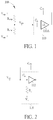
- FIG. 1 is a diagram of an apparatus 100 for performing capacitor amplification in an electronic device according to an embodiment of the present invention, where the apparatus 100 may comprise at least one portion of the electronic device.
- the apparatus 100 may comprise a portion of the electronic device mentioned above, and more particularly, can be at least one hardware circuit such as at least one integrated circuit (IC) within the electronic device and associated circuits thereof.
- the apparatus 100 can be the whole of the electronic device mentioned above.
- the apparatus 100 may comprise a system comprising the electronic device mentioned above (e.g. a wireless communications system comprising the electronic device).
- Examples of the electronic device may include, but not limited to, a multifunctional mobile phone, a tablet, a wearable device, and a laptop computer.
- the apparatus 100 may comprise a first resistor R cmp and a second resistor R cmn that are connected in series and coupled between a set of input terminals of a receiver in the electronic device, such as two input terminals V inp and V inn of the receiver, and may comprise a common mode capacitor C cm having a first terminal (e.g. the left terminal thereof in the architecture shown in FIG. 1 ) coupled to a common mode terminal V cm and having a second terminal (e.g. the right terminal thereof in the architecture shown in FIG. 1 ).
- the two input terminals V inp and V inn may be two differential input terminals, and all input terminals of the set of input terminals comprising the two input terminals V inp and V inn may be voltage input terminals.
- the apparatus 100 may further comprise a capacitor amplification circuit 110 that is utilized as a capacitor multiplier.
- the capacitor amplification circuit 110 of this embodiment may comprise an alternating current (AC) -coupled amplifier 110A that is coupled between the common mode terminal V cm and the second terminal of the common mode capacitor C cm .
- the AC-coupled amplifier 110A may have an input terminal (e.g. the left terminal thereof in the architecture shown in FIG. 1 ) and an output terminal (e.g.
- the capacitor amplification circuit 110 may further comprise an AC-coupling capacitor C b that may be arranged for coupling (e.g., AC-coupling) the input terminal of the AC-coupled amplifier 110A to the common mode terminal V cm , where the AC-coupling capacitor C b may have a first terminal (e.g. the left terminal thereof in the architecture shown in FIG. 1 ) coupled to the common mode terminal V cm , and may have a second terminal (e.g.
- the gain of the AC-coupled amplifier 110A may be equal to -A (e.g. the parameter A is a positive value that is equal to or greater than one, and may be defined as the inband gain of the AC-coupled amplifier 110A), and therefore, the AC-coupled amplifier 110A is labeled "-A" in FIG. 1 , for better comprehension.
- C cm the capacitance value (i.e. the real capacitance value) of the common mode capacitor C cm .
- all of these components may be implemented on an IC such as that mentioned above.
- the first resistor and the second resistor may be arranged for obtaining a common mode voltage V cm at the common mode terminal V cm between the first resistor R cmp and the second resistor R cmn , and the common mode capacitor Ccm may be arranged for reducing a common mode return loss.
- the AC-coupled amplifier 110A may be arranged for performing capacitor amplification for the common mode capacitor C cm .
- operations of the capacitor amplification circuit 110 may make the common mode capacitor C cm to have the equivalent capacitance C cm-Eq that is greater than the real capacitance value C cm of the common mode capacitor C cm .
- the capacitor amplification circuit 110 may emulate greater capacitance of the common mode capacitor C cm than the common mode capacitor C cm really have.
- the apparatus 100 can guarantee the performance of the receiver and the overall performance of the whole system without further increasing the size of the common mode capacitor C cm (e.g. having no need to reserve a larger sub-area on the IC for implementing the common mode capacitor C cm ), since the capacitor amplification circuit 110 may make the capacitance of the common mode capacitor C cm seem to become greater than 100 pF.
- the apparatus 100 can perform capacitor amplification for the common mode capacitor C cm without introducing additional problems such as that of the related art (e.g. the problems of needing a wide input range of bandwidth and requiring strong signal driving of an amplifier, the problems of suffering from a slow operation speed and a large input common mode tolerance, and the problems of suffering from DC leakage due to a mismatch issue and suffering from implementing a complicated circuit that still increases the chip are, and needing wide range driving).
- additional problems such as that of the related art (e.g. the problems of needing a wide input range of bandwidth and requiring strong signal driving of an amplifier, the problems of suffering from a slow operation speed and a large input common mode tolerance, and the problems of suffering from DC leakage due to a mismatch issue and suffering from implementing a complicated circuit that still increases the chip are, and needing wide range driving).
- the apparatus 100 may comprise only a portion of the architecture shown in FIG. 1 .
- the apparatus 100 may comprise the receiver.
- the typical value of each of the first resistor R cmp and the second resistor R cmn may be equal to 50 Ohm.
- the typical value of each of the first resistor R cmp and the second resistor R cmn may be equal to any of some other values.
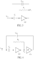
- FIG. 2 illustrates some implementation details of the AC-coupled amplifier 110A shown in FIG. 1 according to an embodiment of the present invention.
- the AC-coupled amplifier 110A shown in FIG. 1 may comprise an inverter 112 and a resistor R b in this embodiment.
- the inverter 112 may have an input terminal (e.g. the left terminal thereof in the architecture shown in FIG. 2 ) coupled to the input terminal of the AC-coupled amplifier 110A, and may have an output terminal (e.g. the right terminal thereof in the architecture shown in FIG. 2 ) coupled to the output terminal of the AC-coupled amplifier 110A.
- the resistor R b may have a first terminal (e.g. the upper terminal thereof in the architecture shown in FIG.
- the bias terminal V b may be utilized for receiving a bias voltage.
- the apparatus 100 can perform capacitor amplification for the common mode capacitor C cm without introducing additional problems such as that of the related art. For example, no wide range amplifier is needed, and no complicated circuit is needed.
- the bias voltage applied to the bias terminal V b may be arbitrarily selected from various kinds of options. Examples of the bias voltage applied to the bias terminal V b may include, but not limited to, a predetermined voltage level, an existing voltage level in the apparatus 100, and a varying voltage level in the architecture shown in any of FIGS. 1-2 .
- FIG. 3 illustrates a hardware configuration of the architecture shown in FIG. 2 according to an embodiment of the present invention.
- the bias terminal Vb may be electrically connected to the output terminal of the inverter 112.
- the output terminal of the inverter 112 may be regarded as the output terminal of the AC-coupled amplifier 110A shown in FIG. 1
- the bias terminal Vb may be coupled to the output terminal of the AC-coupled amplifier 110A shown in FIG. 1 in this embodiment.
- the output terminal of the AC-coupled amplifier 110A e.g. the output terminal of the inverter 112
- the second terminal of the common mode capacitor C cm e.g. the right terminal thereof
- FIG. 4 illustrates some implementation details of the apparatus 100 shown in FIG. 1 according to an embodiment of the present invention.
- the apparatus 100 may further comprise a source follower (SF) 414 that is coupled between the output terminal of the AC-coupled amplifier 110A (e.g. the output terminal of the inverter 112) and the second terminal of the common mode capacitor C cm (e.g. the right terminal thereof).
- SF source follower
- the input terminal of the source follower 414 is coupled to the output terminal of the inverter 112
- the output terminal of the source follower 414 is coupled to second terminal of the common mode capacitor C cm (e.g. the right terminal thereof).
- the source follower 414 may perform capacitor amplification for the common mode capacitor C cm with aid of the source follower 414.
- the source follower 414 may provide the capacitor amplification circuit 110 shown in FIG. 1 with some good features such as low output impedance with proper output power. As a result, the bandwidth of the capacitor amplification operation can be greatly increased. For brevity, similar descriptions for this embodiment are not repeated in detail here.
- FIG. 5 illustrates a gain stage involved with the apparatus 100 shown in FIG. 1 according to an embodiment of the present invention, where the leftmost terminal and the rightmost terminal in the architecture shown in FIG. 5 are the input terminal and the output terminal of the gain stage, respectively.
- the gain stage of this embodiment may comprise a plurality of Metal Oxide Semiconductor Field Effect Transistors (MOSFETs) coupled to each other, such as a P-type MOSFET (PMOSFET) and a N-type MOSFET (NMOSFET) that are coupled between a set of predetermined voltage levels, such as a driving voltage level at a driving terminal and a ground voltage level at a ground terminal.
- MOSFETs Metal Oxide Semiconductor Field Effect Transistors
- the gain stage can be regarded as an inverter circuit INV.
- This gain stage (labeled “INV” in FIG. 5 , for better comprehension) can be utilized for implementing the inverter 112 in the architecture shown in FIG. 3 , and can be utilized for implementing the inverter 112 in the architecture shown in FIG. 4 .
- INV inverter circuit
- FIG. 6 illustrates a gain stage involved with the apparatus 100 shown in FIG. 1 according to another embodiment of the present invention, where the leftmost terminal and the rightmost terminal in the architecture shown in FIG. 6 are the input terminal and the output terminal of the gain stage, respectively.
- the gain stage of this embodiment may comprise the inverter circuit INV, and may further comprise a diode connected MOSFET such as a diode connected NMOSFET coupled between the output terminal and the ground terminal (i.e. the MOSFET shown around the lower right of FIG. 6 ), where two of the three terminals of the diode connected MOSFET, such as the gate terminal thereof and one of the others within the three terminals, are electrically connected to each other.
- a diode connected MOSFET such as a diode connected NMOSFET coupled between the output terminal and the ground terminal (i.e. the MOSFET shown around the lower right of FIG. 6 )
- two of the three terminals of the diode connected MOSFET such as the gate terminal thereof and one of the
- the gain stage can be regarded as a combination of the inverter circuit INV and the diode connected MOSFET having the transconductance gm.
- This gain stage (labeled "INV+1/gm" in FIG. 6 , for better comprehension) can be utilized for implementing the inverter 112 in the architecture shown in FIG. 3 , and can be utilized for implementing the inverter 112 in the architecture shown in FIG. 4 .
- the inverter circuit INV may provide the capacitor amplification circuit 110 shown in FIG. 1 with some good features such as better linearity and less process variation. For brevity, similar descriptions for this embodiment are not repeated in detail here.
- the diode connected MOSFET can be implemented with a diode connected PMOSFET.
- a diode connected PMOSFET for brevity, similar descriptions for this embodiment are not repeated in detail here.
- the inverter 112 shown in FIG. 2 may comprise a first MOSFET and a second MOSFET that are coupled between the set of predetermined voltage levels, such as the PMOSFET and the NMOSFET in the inverter circuit INV of any of the embodiments respectively shown in FIGS. 5-6 .
- the input terminal of the inverter 112 may be electrically connected to the gate terminal of the first MOSFET and the gate terminal of the second MOSFET, and the output terminal of the inverter 112 may be electrically connected to another terminal of the first MOSFET and another terminal of the second MOSFET.
- yet another terminal of the first MOSFET may be electrically connected to one of the set of predetermined voltage levels, and yet another terminal of the second MOSFET may be electrically connected to another of the set of predetermined voltage levels.
- the inverter 112 shown in FIG. 2 may further comprise a third MOSFET having a gate terminal electrically connected to the output terminal of the inverter 112 and having other terminals, such as the diode connected MOSFET mentioned in the embodiment shown in FIG. 6 .
- one of the other terminals of the third MOSFET may be electrically connected to the aforementioned one of the set of predetermined voltage levels, and another of the other terminals of the third MOSFET may be electrically connected to the output terminal of the inverter.
- similar descriptions for these embodiments are not repeated in detail here.
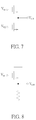
- FIG. 7 illustrates a source follower circuit involved with the apparatus 100 shown in FIG. 1 according to an embodiment of the present invention, where the terminals V in and V out are the input terminal and the output terminal of the source follower circuit, respectively.
- the bias terminal Vb2 of the source follower circuit is arranged for receiving a predetermined bias voltage, for controlling the MOSFET shown in the lower half of FIG. 7 to stay in the saturation region thereof.
- the source follower circuit of this embodiment can be utilized for implementing the source follower 414 shown in FIG. 4 . For brevity, similar descriptions for this embodiment are not repeated in detail here.
- FIG. 8 illustrates a source follower circuit involved with the apparatus 100 shown in FIG. 1 according to another embodiment of the present invention, where the terminals V in and V out are the input terminal and the output terminal of the source follower circuit, respectively.
- one of the MOSFETs can be replaced by a resistor in this embodiment.
- the source follower circuit of this embodiment can be utilized for implementing the source follower 414 shown in FIG. 4 .
- similar descriptions for this embodiment are not repeated in detail here.
- the receiver may comply with a specific specification such as the band-pass common-mode return loss (i.e., band-pass SCC11) specification, and the AC-coupled amplifier 110A of any of the above embodiments is especially suitable for performing capacitor amplification, to guarantee the performance of the receiver and the overall performance of the whole system without further increasing the size of the common mode capacitor C cm .
- band-pass SCC11 means the specification defines the required SCC11 from a specific lowest frequency to a specific highest frequency.
- the AC-coupled amplifier 110A can tolerate a larger transmitter (TX) common-mode input level than that of the related art.
- the AC-coupled amplifier 110A may be implemented in a core device to further increase the operation speed of the receiver.
Landscapes
- Engineering & Computer Science (AREA)
- Power Engineering (AREA)
- Amplifiers (AREA)
Abstract
Description
- The present invention relates to alternating current (AC)-coupled capacitor amplification for common-mode termination, and more particularly, to an apparatus for performing capacitor amplification in an electronic device according to the pre-characterizing clauses of
claim 1. - According to the related art, a direct current (DC) coupling system may be designed to have a floating termination architecture, and it looks like open circuit in one or more situations. Based on this design, some problems may occur. For example, a capacitor having a capacitance value of more than one hundred picofarad (pF) may be required, causing the associated chip area to be increased. As a result, the associated costs are increased. Some conventional methods are proposed to try solving the problems, but additional problems such as some side effects may occur. For example, a receiver may need a wide input range of bandwidth and may require strong signal driving of an amplifier, causing increased costs and increased power consumption. In another example, a receiver may suffer from a slow operation speed and a large input common mode tolerance. In another example, a receiver may suffer from DC leakage due to a mismatch issue and suffer from implementing a complicated circuit that still increases the chip are, and may need wide range driving. Thus, a novel architecture is required for performing capacitor amplification, in order to save the chip area.
- It is an objective of the claimed invention to provide an apparatus for performing capacitor amplification in an electronic device, in order to solve the above-mentioned problems.
- It is another objective of the claimed invention to provide an apparatus for performing capacitor amplification in an electronic device, in order to guarantee the overall performance of the whole system.
- According to at least one preferred embodiment, an apparatus for performing capacitor amplification in an electronic device is provided, where the apparatus may comprise at least one portion (e.g. a portion or all) of the electronic device. For example, the apparatus may comprise a first resistor and a second resistor that are connected in series and coupled between a set of input terminals of a receiver in the electronic device, and may comprise a common mode capacitor having a first terminal coupled to a common mode terminal and having a second terminal, and may further comprise an alternating current (AC)-coupled amplifier that is coupled between the common mode terminal and the second terminal of the common mode capacitor. The first resistor and the second resistor may be arranged for obtaining a common mode voltage at the common mode terminal between the first resistor and the second resistor. In addition, the common mode capacitor may be arranged for reducing a common mode return loss. Additionally, the AC-coupled amplifier may be arranged for performing capacitor amplification for the common mode capacitor.
- It is an advantage of the present invention that the present invention apparatus can guarantee the overall performance of the whole system. For example, by using the AC-coupled amplifier, the present invention apparatus can reduce the required input dynamic range. In addition, the present invention apparatus can use the AC-coupled amplifier to perform capacitor amplification on the common mode capacitor. By using the AC-coupled amplifier, the required capacitance value of the common mode capacitor can be greatly decreased without degrading the performance of the whole system, and therefore the present invention apparatus eliminates the need of implementing a capacitor having a capacitance value of more than one hundred picofarad (pF) for a direct current (DC) coupling system such as that mentioned above, so the chip area of an integrated circuit (IC) can be saved. As a result, the related art problems can be prevented.
- In the following, the invention is further illustrated by way of example, taking reference to the accompanying drawings.
-
FIG. 1 is a diagram of an apparatus for performing capacitor amplification in an electronic device according to an embodiment of the present invention, -
FIG. 2 illustrates some implementation details of the alternating current (AC)-coupled amplifier shown inFIG. 1 according to an embodiment of the present invention, -
FIG. 3 illustrates a hardware configuration of the AC-coupled amplifier shown inFIG. 2 according to an embodiment of the present invention, -
FIG. 4 illustrates some implementation details of the apparatus shown inFIG. 1 according to an embodiment of the present invention, -
FIG. 5 illustrates a gain stage involved with the apparatus shown inFIG. 1 according to an embodiment of the present invention, -
FIG. 6 illustrates a gain stage involved with the apparatus shown inFIG. 1 according to another embodiment of the present invention, -
FIG. 7 illustrates a source follower circuit involved with the apparatus shown inFIG. 1 according to an embodiment of the present invention, and -
FIG. 8 illustrates a source follower circuit involved with the apparatus shown inFIG. 1 according to another embodiment of the present invention. - Certain terms are used throughout the following description and claims, which refer to particular components. As one skilled in the art will appreciate, electronic equipment manufacturers may refer to a component by different names. This document does not intend to distinguish between components that differ in name but not in function. In the following description and in the claims, the terms "include" and "comprise" are used in an open-ended fashion, and thus should be interpreted to mean "include, but not limited to ... ". Also, the term "couple" is intended to mean either an indirect or direct electrical connection. Accordingly, if one device is coupled to another device, that connection may be through a direct electrical connection, or through an indirect electrical connection via other devices and connections.
-
FIG. 1 is a diagram of anapparatus 100 for performing capacitor amplification in an electronic device according to an embodiment of the present invention, where theapparatus 100 may comprise at least one portion of the electronic device. For example, theapparatus 100 may comprise a portion of the electronic device mentioned above, and more particularly, can be at least one hardware circuit such as at least one integrated circuit (IC) within the electronic device and associated circuits thereof. In another example, theapparatus 100 can be the whole of the electronic device mentioned above. In another example, theapparatus 100 may comprise a system comprising the electronic device mentioned above (e.g. a wireless communications system comprising the electronic device). Examples of the electronic device may include, but not limited to, a multifunctional mobile phone, a tablet, a wearable device, and a laptop computer. - As shown in
FIG. 1 , theapparatus 100 may comprise a first resistor Rcmp and a second resistor Rcmn that are connected in series and coupled between a set of input terminals of a receiver in the electronic device, such as two input terminals Vinp and Vinn of the receiver, and may comprise a common mode capacitor Ccm having a first terminal (e.g. the left terminal thereof in the architecture shown inFIG. 1 ) coupled to a common mode terminal Vcm and having a second terminal (e.g. the right terminal thereof in the architecture shown inFIG. 1 ). For example, the two input terminals Vinp and Vinn may be two differential input terminals, and all input terminals of the set of input terminals comprising the two input terminals Vinp and Vinn may be voltage input terminals. In addition, theapparatus 100 may further comprise acapacitor amplification circuit 110 that is utilized as a capacitor multiplier. As shown inFIG. 1 , thecapacitor amplification circuit 110 of this embodiment may comprise an alternating current (AC) -coupledamplifier 110A that is coupled between the common mode terminal Vcm and the second terminal of the common mode capacitor Ccm. For example, the AC-coupledamplifier 110A may have an input terminal (e.g. the left terminal thereof in the architecture shown inFIG. 1 ) and an output terminal (e.g. the right terminal thereof in the architecture shown inFIG. 1 ), and the input terminal of the AC-coupledamplifier 110A may be coupled to the common mode terminal Vcm, and the output terminal of the AC-coupledamplifier 110A may be coupled to the second terminal of the common mode capacitor Ccm. According to this embodiment, thecapacitor amplification circuit 110 may further comprise an AC-coupling capacitor Cb that may be arranged for coupling (e.g., AC-coupling) the input terminal of the AC-coupledamplifier 110A to the common mode terminal Vcm, where the AC-coupling capacitor Cb may have a first terminal (e.g. the left terminal thereof in the architecture shown inFIG. 1 ) coupled to the common mode terminal Vcm, and may have a second terminal (e.g. the right terminal thereof in the architecture shown inFIG. 1 ) coupled to the input terminal of the AC-coupled amplifier. For example, by properly designing the AC-coupledamplifier 110A, the gain of the AC-coupledamplifier 110A may be equal to -A (e.g. the parameter A is a positive value that is equal to or greater than one, and may be defined as the inband gain of the AC-coupledamplifier 110A), and therefore, the AC-coupledamplifier 110A is labeled "-A" inFIG. 1 , for better comprehension. As a result of utilizing the AC-coupledamplifier 110A, the equivalent capacitance Ccm-Eq of the common mode capacitor Ccm may be express as follows:
- According to this embodiment, the first resistor and the second resistor may be arranged for obtaining a common mode voltage Vcm at the common mode terminal Vcm between the first resistor Rcmp and the second resistor Rcmn, and the common mode capacitor Ccm may be arranged for reducing a common mode return loss. In addition, the AC-coupled
amplifier 110A may be arranged for performing capacitor amplification for the common mode capacitor Ccm. For example, operations of thecapacitor amplification circuit 110 may make the common mode capacitor Ccm to have the equivalent capacitance Ccm-Eq that is greater than the real capacitance value Ccm of the common mode capacitor Ccm. In this embodiment, thecapacitor amplification circuit 110 may emulate greater capacitance of the common mode capacitor Ccm than the common mode capacitor Ccm really have. For example, in a situation where the capacitance value Ccm of the common mode capacitor Ccm does not reach 100 picofarad (pF), by utilizing thecapacitor amplification circuit 110, theapparatus 100 can guarantee the performance of the receiver and the overall performance of the whole system without further increasing the size of the common mode capacitor Ccm (e.g. having no need to reserve a larger sub-area on the IC for implementing the common mode capacitor Ccm), since thecapacitor amplification circuit 110 may make the capacitance of the common mode capacitor Ccm seem to become greater than 100 pF. - Based on the architecture shown in
FIG. 1 , theapparatus 100 can perform capacitor amplification for the common mode capacitor Ccm without introducing additional problems such as that of the related art (e.g. the problems of needing a wide input range of bandwidth and requiring strong signal driving of an amplifier, the problems of suffering from a slow operation speed and a large input common mode tolerance, and the problems of suffering from DC leakage due to a mismatch issue and suffering from implementing a complicated circuit that still increases the chip are, and needing wide range driving). - For better comprehension, the first resistor Rcmp and the second resistor Rcmn, together with the two input terminals Vinp and Vinn of the receiver, are illustrated in
FIG. 1 . According to some embodiments, theapparatus 100 may comprise only a portion of the architecture shown inFIG. 1 . According to some embodiments, theapparatus 100 may comprise the receiver. In some embodiments, such as the embodiment shown inFIG. 1 , the typical value of each of the first resistor Rcmp and the second resistor Rcmn may be equal to 50 Ohm. In some embodiments, the typical value of each of the first resistor Rcmp and the second resistor Rcmn may be equal to any of some other values. -
FIG. 2 illustrates some implementation details of the AC-coupledamplifier 110A shown inFIG. 1 according to an embodiment of the present invention. For example, the AC-coupledamplifier 110A shown inFIG. 1 may comprise aninverter 112 and a resistor Rb in this embodiment. Theinverter 112 may have an input terminal (e.g. the left terminal thereof in the architecture shown inFIG. 2 ) coupled to the input terminal of the AC-coupledamplifier 110A, and may have an output terminal (e.g. the right terminal thereof in the architecture shown inFIG. 2 ) coupled to the output terminal of the AC-coupledamplifier 110A. In addition, the resistor Rb may have a first terminal (e.g. the upper terminal thereof in the architecture shown inFIG. 2 ) coupled to the input terminal of the AC-coupledamplifier 110A, and may have a second terminal (e.g. the lower terminal thereof in the architecture shown inFIG. 2 ) that is electrically connected to a bias terminal Vb, where the bias terminal Vb may be utilized for receiving a bias voltage. - By using the architecture shown in
FIG. 2 , theapparatus 100 can perform capacitor amplification for the common mode capacitor Ccm without introducing additional problems such as that of the related art. For example, no wide range amplifier is needed, and no complicated circuit is needed. In addition, as long as performing capacitor amplification for the common mode capacitor Ccm will not be hindered, the bias voltage applied to the bias terminal Vb may be arbitrarily selected from various kinds of options. Examples of the bias voltage applied to the bias terminal Vb may include, but not limited to, a predetermined voltage level, an existing voltage level in theapparatus 100, and a varying voltage level in the architecture shown in any ofFIGS. 1-2 . -
FIG. 3 illustrates a hardware configuration of the architecture shown inFIG. 2 according to an embodiment of the present invention. As shown inFIG. 3 , the bias terminal Vb may be electrically connected to the output terminal of theinverter 112. In addition, as the output terminal of theinverter 112 may be regarded as the output terminal of the AC-coupledamplifier 110A shown inFIG. 1 , the bias terminal Vb may be coupled to the output terminal of the AC-coupledamplifier 110A shown inFIG. 1 in this embodiment. Based on the architecture shown inFIG. 3 , the output terminal of the AC-coupledamplifier 110A (e.g. the output terminal of the inverter 112) and the second terminal of the common mode capacitor Ccm (e.g. the right terminal thereof) are electrically connected to each other, directly. For brevity, similar descriptions for this embodiment are not repeated in detail here. -
FIG. 4 illustrates some implementation details of theapparatus 100 shown inFIG. 1 according to an embodiment of the present invention. As shown inFIG. 4 , theapparatus 100 may further comprise a source follower (SF) 414 that is coupled between the output terminal of the AC-coupledamplifier 110A (e.g. the output terminal of the inverter 112) and the second terminal of the common mode capacitor Ccm (e.g. the right terminal thereof). For example, the input terminal of thesource follower 414 is coupled to the output terminal of theinverter 112, and the output terminal of thesource follower 414 is coupled to second terminal of the common mode capacitor Ccm (e.g. the right terminal thereof). Based on the architecture shown inFIG. 4 , thecapacitor amplification circuit 110 shown inFIG. 1 may comprise thesource follower 414, and may perform capacitor amplification for the common mode capacitor Ccm with aid of thesource follower 414. For example, during perform capacitor amplification for the common mode capacitor Ccm, thesource follower 414 may provide thecapacitor amplification circuit 110 shown inFIG. 1 with some good features such as low output impedance with proper output power. As a result, the bandwidth of the capacitor amplification operation can be greatly increased. For brevity, similar descriptions for this embodiment are not repeated in detail here. -
FIG. 5 illustrates a gain stage involved with theapparatus 100 shown inFIG. 1 according to an embodiment of the present invention, where the leftmost terminal and the rightmost terminal in the architecture shown inFIG. 5 are the input terminal and the output terminal of the gain stage, respectively. For example, the gain stage of this embodiment may comprise a plurality of Metal Oxide Semiconductor Field Effect Transistors (MOSFETs) coupled to each other, such as a P-type MOSFET (PMOSFET) and a N-type MOSFET (NMOSFET) that are coupled between a set of predetermined voltage levels, such as a driving voltage level at a driving terminal and a ground voltage level at a ground terminal. Based on the architecture shown inFIG. 5 , the gain stage can be regarded as an inverter circuit INV. This gain stage (labeled "INV" inFIG. 5 , for better comprehension) can be utilized for implementing theinverter 112 in the architecture shown inFIG. 3 , and can be utilized for implementing theinverter 112 in the architecture shown inFIG. 4 . For brevity, similar descriptions for this embodiment are not repeated in detail here. -
FIG. 6 illustrates a gain stage involved with theapparatus 100 shown inFIG. 1 according to another embodiment of the present invention, where the leftmost terminal and the rightmost terminal in the architecture shown inFIG. 6 are the input terminal and the output terminal of the gain stage, respectively. For example, the gain stage of this embodiment may comprise the inverter circuit INV, and may further comprise a diode connected MOSFET such as a diode connected NMOSFET coupled between the output terminal and the ground terminal (i.e. the MOSFET shown around the lower right ofFIG. 6 ), where two of the three terminals of the diode connected MOSFET, such as the gate terminal thereof and one of the others within the three terminals, are electrically connected to each other. Based on the arrangement in the architecture shown inFIG. 6 , the gain stage can be regarded as a combination of the inverter circuit INV and the diode connected MOSFET having the transconductance gm. This gain stage (labeled "INV+1/gm" inFIG. 6 , for better comprehension) can be utilized for implementing theinverter 112 in the architecture shown inFIG. 3 , and can be utilized for implementing theinverter 112 in the architecture shown inFIG. 4 . With aid of the diode connected MOSFET, the inverter circuit INV may provide thecapacitor amplification circuit 110 shown inFIG. 1 with some good features such as better linearity and less process variation. For brevity, similar descriptions for this embodiment are not repeated in detail here. - According to some embodiments, the diode connected MOSFET can be implemented with a diode connected PMOSFET. For brevity, similar descriptions for this embodiment are not repeated in detail here.
- According to some embodiments, the
inverter 112 shown inFIG. 2 may comprise a first MOSFET and a second MOSFET that are coupled between the set of predetermined voltage levels, such as the PMOSFET and the NMOSFET in the inverter circuit INV of any of the embodiments respectively shown inFIGS. 5-6 . In addition, the input terminal of theinverter 112 may be electrically connected to the gate terminal of the first MOSFET and the gate terminal of the second MOSFET, and the output terminal of theinverter 112 may be electrically connected to another terminal of the first MOSFET and another terminal of the second MOSFET. Additionally, yet another terminal of the first MOSFET may be electrically connected to one of the set of predetermined voltage levels, and yet another terminal of the second MOSFET may be electrically connected to another of the set of predetermined voltage levels. For brevity, similar descriptions for these embodiments are not repeated in detail here. - According to some embodiments, the
inverter 112 shown inFIG. 2 may further comprise a third MOSFET having a gate terminal electrically connected to the output terminal of theinverter 112 and having other terminals, such as the diode connected MOSFET mentioned in the embodiment shown inFIG. 6 . In addition, one of the other terminals of the third MOSFET may be electrically connected to the aforementioned one of the set of predetermined voltage levels, and another of the other terminals of the third MOSFET may be electrically connected to the output terminal of the inverter. For brevity, similar descriptions for these embodiments are not repeated in detail here. -
FIG. 7 illustrates a source follower circuit involved with theapparatus 100 shown inFIG. 1 according to an embodiment of the present invention, where the terminals Vin and Vout are the input terminal and the output terminal of the source follower circuit, respectively. The bias terminal Vb2 of the source follower circuit is arranged for receiving a predetermined bias voltage, for controlling the MOSFET shown in the lower half ofFIG. 7 to stay in the saturation region thereof. The source follower circuit of this embodiment can be utilized for implementing thesource follower 414 shown inFIG. 4 . For brevity, similar descriptions for this embodiment are not repeated in detail here. -
FIG. 8 illustrates a source follower circuit involved with theapparatus 100 shown inFIG. 1 according to another embodiment of the present invention, where the terminals Vin and Vout are the input terminal and the output terminal of the source follower circuit, respectively. In comparison with the architecture shown inFIG. 7 , one of the MOSFETs can be replaced by a resistor in this embodiment. The source follower circuit of this embodiment can be utilized for implementing thesource follower 414 shown inFIG. 4 . For brevity, similar descriptions for this embodiment are not repeated in detail here. - According to some embodiments, the receiver may comply with a specific specification such as the band-pass common-mode return loss (i.e., band-pass SCC11) specification, and the AC-coupled
amplifier 110A of any of the above embodiments is especially suitable for performing capacitor amplification, to guarantee the performance of the receiver and the overall performance of the whole system without further increasing the size of the common mode capacitor Ccm. Here, the term "band-pass SCC11" means the specification defines the required SCC11 from a specific lowest frequency to a specific highest frequency. For example, in a situation where a designer of the electronic device only cares about a specific frequency band above 50 megahertz (MHz) to a few gigahertz (GHz), with the ac-coupling, the AC-coupledamplifier 110A can tolerate a larger transmitter (TX) common-mode input level than that of the related art. In some embodiments, the AC-coupledamplifier 110A may be implemented in a core device to further increase the operation speed of the receiver. - Those skilled in the art will readily observe that numerous modifications and alterations of the device and method may be made while retaining the teachings of the invention. Accordingly, the above disclosure should be construed as limited only by the metes and bounds of the appended claims.
Claims (12)
- An apparatus (100) for performing capacitor amplification in an electronic device, characterized by:a first resistor (Rcmp) and a second resistor (Rcmn), connected in series and coupled between a set of input terminals of a receiver in the electronic device, arranged for obtaining a common mode voltage (Vcm) at a common mode terminal (Vcm) between the first resistor (Rcmp) and the second resistor (Rcmn);a common mode capacitor (Ccm), having a first terminal coupled to the common mode terminal (Vcm) and having a second terminal, arranged for reducing a common mode return loss; andan alternating current-coupled amplifier (110A), hereinafter AC-coupled amplifier, coupled between the common mode terminal (Vcm) and the second terminal of the common mode capacitor, arranged for performing capacitor amplification for the common mode capacitor (Ccm).
- The apparatus (100) of claim 1, characterized in that the set of input terminals comprises two differential input terminals.
- The apparatus (100) of claim 1, characterized in that all input terminals of the set of input terminals are voltage input terminals.
- The apparatus (100) of claim 1, characterized in that the AC-coupled amplifier (110) has an input terminal and an output terminal; and the input terminal of the AC-coupled amplifier (110) is coupled to the common mode terminal (Vcm), and the output terminal of the AC-coupled amplifier (110) is coupled to the second terminal of the common mode capacitor (Ccm).
- The apparatus (100) of claim 4, characterized in that the apparatus (100) further comprises:an alternating current-coupling capacitor (Cb), hereinafter AC-coupling capacitor, arranged for coupling the input terminal of the AC-coupled amplifier (110A) to the common mode terminal (Vcm), wherein the AC-coupling capacitor (Cb) has a first terminal coupled to the common mode terminal (Vcm), and has a second terminal coupled to the input terminal of the AC-coupled amplifier (110A).
- The apparatus (100) of claim 4, characterized in that a gain of the AC-coupled amplifier (110A) is equal to -A, wherein the parameter A is a positive value that is equal to or greater than one.
- The apparatus (100) of claim 4, characterized in that the AC-coupled amplifier (110A) comprises:an inverter (112), having an input terminal coupled to the input terminal of the AC-coupled amplifier (110A), and having an output terminal coupled to the output terminal of the AC-coupled amplifier (110A); anda resistor (Rb), having a first terminal coupled to the input terminal of the AC-coupled amplifier (110A), and having a second terminal coupled to the output terminal of the AC-coupled amplifier (110A).
- The apparatus (100) of claim 7, characterized in that the output terminal of the AC-coupled amplifier (110A) and the second terminal of the common mode capacitor (Ccm) are electrically connected to each other, directly.
- The apparatus (100) of claim 7, characterized in that the apparatus (100) further comprises:a source follower (414), coupled between the output terminal of the AC-coupled amplifier (110A) and the second terminal of the common mode capacitor (Ccm).
- The apparatus (100) of claim 7, characterized in that the inverter (112) comprises:a first Metal Oxide Semiconductor Field Effect Transistor, hereinafter MOSFET, and a second MOSFET, coupled between a set of predetermined voltage levels, wherein the input terminal of the inverter (112) is electrically connected to a gate terminal of the first MOSFET and a gate terminal of the second MOSFET, and the output terminal of the inverter (112) is electrically connected to another terminal of the first MOSFET and another terminal of the second MOSFET, wherein yet another terminal of the first MOSFET is electrically connected to one of the set of predetermined voltage levels, and yet another terminal of the second MOSFET is electrically connected to another of the set of predetermined voltage levels.
- The apparatus (100) of claim 10, characterized in that the inverter (112) further comprises:a third MOSFET, having a gate terminal electrically connected to the output terminal of the inverter (112) and having other terminals, wherein one of the other terminals of the third MOSFET is electrically connected to the one of the set of predetermined voltage levels, and another of the other terminals of the third MOSFET is electrically connected to the output terminal of the inverter.
- The apparatus (100) of claim 1, characterized in that the apparatus (100) comprises the receiver.
Applications Claiming Priority (2)
| Application Number | Priority Date | Filing Date | Title |
|---|---|---|---|
| US201562222434P | 2015-09-23 | 2015-09-23 | |
| US15/147,902 US9800219B2 (en) | 2015-09-23 | 2016-05-05 | Apparatus for performing capacitor amplification in an electronic device |
Publications (1)
| Publication Number | Publication Date |
|---|---|
| EP3148073A1 true EP3148073A1 (en) | 2017-03-29 |
Family
ID=56024165
Family Applications (1)
| Application Number | Title | Priority Date | Filing Date |
|---|---|---|---|
| EP16170308.7A Withdrawn EP3148073A1 (en) | 2015-09-23 | 2016-05-19 | Apparatus for performing capacitor amplification in an electronic device |
Country Status (3)
| Country | Link |
|---|---|
| US (1) | US9800219B2 (en) |
| EP (1) | EP3148073A1 (en) |
| CN (1) | CN106549643A (en) |
Citations (1)
| Publication number | Priority date | Publication date | Assignee | Title |
|---|---|---|---|---|
| EP1748551A2 (en) * | 2005-07-29 | 2007-01-31 | Broadcom Corporation | Current-controlled CMOS (C3MOS) wideband input data amplifier for reduced differential and common-mode reflection |
Family Cites Families (6)
| Publication number | Priority date | Publication date | Assignee | Title |
|---|---|---|---|---|
| JPH06150033A (en) * | 1992-11-06 | 1994-05-31 | Takayama:Kk | Weighted adder circuit |
| JPH0746083A (en) * | 1993-07-27 | 1995-02-14 | Toshiba Corp | Speech synthesis and band limiting circuit and bass boost circuit |
| CN100472947C (en) * | 2005-07-29 | 2009-03-25 | 美国博通公司 | Current Controlled Silicon Complementary Metal Oxide Semiconductor Broadband Data Amplifier Circuit |
| US7414471B2 (en) * | 2006-06-06 | 2008-08-19 | Texas Instruments Incorporated | Common-mode technique for a digital I/P class D loop |
| US7995660B2 (en) | 2007-10-31 | 2011-08-09 | International Business Machines Corporation | Receiver termination circuit for a high speed direct current (DC) serial link |
| US8664973B2 (en) | 2012-08-06 | 2014-03-04 | Broadcom Corporation | Common mode termination with C-multiplier circuit |
-
2016
- 2016-05-05 US US15/147,902 patent/US9800219B2/en active Active
- 2016-05-19 EP EP16170308.7A patent/EP3148073A1/en not_active Withdrawn
- 2016-06-08 CN CN201610405771.8A patent/CN106549643A/en not_active Withdrawn
Patent Citations (1)
| Publication number | Priority date | Publication date | Assignee | Title |
|---|---|---|---|---|
| EP1748551A2 (en) * | 2005-07-29 | 2007-01-31 | Broadcom Corporation | Current-controlled CMOS (C3MOS) wideband input data amplifier for reduced differential and common-mode reflection |
Non-Patent Citations (8)
| Title |
|---|
| "Design of Analog CMOS integrated circuits", 1 January 2001, MCGRAW-HILL, Singapore, ISBN: 978-0-07-118839-5, article BEHZAD RAZAVI: "Design of Analog CMOS integrated circuits", pages: 166 - 171, XP055422985 * |
| COSTA ARTHUR LIRANETO TORRES ET AL: "A 2-decades wideband low-noise amplifier with high gain and ESD protection", 2015 28TH SYMPOSIUM ON INTEGRATED CIRCUITS AND SYSTEMS DESIGN (SBCCI), ACM, 31 August 2015 (2015-08-31), pages 1 - 6, XP032894654 * |
| GU J ET AL: "Distributed active decoupling capacitors for on-chip supply noise cancellation in digital VLSI circuits", VLSI CIRCUITS, 2006. DIGEST OF TECHNICAL PAPERS. 2006 SYMPOSIUM ON, 1 January 2006 (2006-01-01), IEEE, XP002766305, DOI: 10.1109/VLSIC.2006.1705387 * |
| HASHIMOTO Y ET AL: "An On-Chip Active Decoupling Circuit to Suppress Crosstalk in Deep-Submicron CMOS Mixed-Signal SoCs", IEEE JOURNAL OF SOLID-STATE CIRCUITS, vol. 40, no. 1, 1 January 2005 (2005-01-01), IEEE SERVICE CENTER, PISCATAWAY, NJ, USA, pages 67 - 79, XP011124404, ISSN: 0018-9200, DOI: 10.1109/JSSC.2004.838010 * |
| JIE GU ET AL: "Design and Implementation of Active Decoupling Capacitor Circuits for Power Supply Regulation in Digital ICs", IEEE TRANSACTIONS ON VERY LARGE SCALE INTEGRATION (VLSI) SYSTEMS, vol. 16, no. 2, 1 February 2009 (2009-02-01), IEEE SERVICE CENTER, PISCATAWAY, NJ, USA, pages 292 - 301, XP011241138, ISSN: 1063-8210, DOI: 10.1109/TVLSI.2008.2004543 * |
| LIN CHUNG-CHING ET AL: "A 23.2 dBm linear power amplifier using pre-distortion technique for LTE applications", 2014 12TH IEEE INTERNATIONAL CONFERENCE ON SOLID-STATE AND INTEGRATED CIRCUIT TECHNOLOGY (ICSICT), IEEE, 28 October 2014 (2014-10-28), pages 1 - 3, XP032727385, ISBN: 978-1-4799-3296-2, [retrieved on 20150123], DOI: 10.1109/ICSICT.2014.7021472 * |
| QI GENG-ZHEN ET AL: "A wideband multi-stage inverter-based driver amplifier for IEEE 802.22 WRAN transmitters", FIFTH ASIA SYMPOSIUM ON QUALITY ELECTRONIC DESIGN (ASQED 2013), IEEE, 26 August 2013 (2013-08-26), pages 6 - 9, XP032513958, DOI: 10.1109/ASQED.2013.6643554 * |
| SEIEDHOSSEINZADEH N ET AL: "Low noise amplifier linearization for near millimeter wave band applications", MILLIMETER -WAVE AND TERAHERTZ TECHNOLOGIES (MMWATT), 2012 SECOND CONFERENCE ON, IEEE, 24 December 2012 (2012-12-24), pages 48 - 51, XP032777713, ISSN: 2157-0965, ISBN: 978-1-4673-4954-3, [retrieved on 20130613], DOI: 10.1109/MMWATT.2012.6532165 * |
Also Published As
| Publication number | Publication date |
|---|---|
| US20170085234A1 (en) | 2017-03-23 |
| US9800219B2 (en) | 2017-10-24 |
| CN106549643A (en) | 2017-03-29 |
Similar Documents
| Publication | Publication Date | Title |
|---|---|---|
| US9191004B2 (en) | Signal converting device and digital transmitting apparatus applying the signal converting device | |
| US9319043B2 (en) | Generation of differential signals | |
| CN106026952B (en) | Device and method for the common source and common grid amplifier topological structure for millimeter wave power application | |
| US11264984B2 (en) | Single supply RF switch driver | |
| US10243564B2 (en) | Input-output receiver | |
| JP4832965B2 (en) | Switch circuit device, radio circuit device using the switch circuit device, and sampling circuit device | |
| US12081211B2 (en) | High power positive logic switch | |
| CN111865283B (en) | High power radio frequency switch with low leakage current and low insertion loss | |
| US20170187399A1 (en) | Transmitter output driver circuits for high data rate applications, and methods of their operation | |
| US20140253233A1 (en) | Current Conveyor Circuit and Method | |
| CN101826859B (en) | Signal source device and signal source device for generating output signal | |
| CN102447458B (en) | Switching device | |
| US10135442B2 (en) | Current-mode logic circuit | |
| US11764744B2 (en) | Distributed circuit | |
| US10305481B2 (en) | Pre-driver for driving low voltage differential signaling (LVDS) driving circuit | |
| US20230396244A1 (en) | Methods and devices for fast switching of radio frequency switches | |
| US11973470B2 (en) | Impedance control in merged stacked FET amplifiers | |
| CN108400791B (en) | Radio frequency transceiver and radio frequency transmitter thereof | |
| US9800219B2 (en) | Apparatus for performing capacitor amplification in an electronic device | |
| US8922450B2 (en) | Signal converting circuit capable of reducing/avoiding signal leakage and related signal converting method | |
| US20150256179A1 (en) | Switching control circuit and wireless communication device | |
| US10404312B2 (en) | Signal processing apparatus | |
| US10057093B2 (en) | Using common mode local oscillator termination in single-ended commutating circuits for conversion gain improvement | |
| CN116015272A (en) | Level conversion circuits, radio frequency switches and electronic equipment | |
| JP2007243410A (en) | High frequency switch circuit and semiconductor device using the same |
Legal Events
| Date | Code | Title | Description |
|---|---|---|---|
| PUAI | Public reference made under article 153(3) epc to a published international application that has entered the european phase |
Free format text: ORIGINAL CODE: 0009012 |
|
| AK | Designated contracting states |
Kind code of ref document: A1 Designated state(s): AL AT BE BG CH CY CZ DE DK EE ES FI FR GB GR HR HU IE IS IT LI LT LU LV MC MK MT NL NO PL PT RO RS SE SI SK SM TR |
|
| AX | Request for extension of the european patent |
Extension state: BA ME |
|
| 17P | Request for examination filed |
Effective date: 20170720 |
|
| RBV | Designated contracting states (corrected) |
Designated state(s): AL AT BE BG CH CY CZ DE DK EE ES FI FR GB GR HR HU IE IS IT LI LT LU LV MC MK MT NL NO PL PT RO RS SE SI SK SM TR |
|
| 17Q | First examination report despatched |
Effective date: 20171117 |
|
| STAA | Information on the status of an ep patent application or granted ep patent |
Free format text: STATUS: THE APPLICATION IS DEEMED TO BE WITHDRAWN |
|
| 18D | Application deemed to be withdrawn |
Effective date: 20180822 |