EP3148040A1 - Charging circuit and mobile terminal - Google Patents
Charging circuit and mobile terminal Download PDFInfo
- Publication number
- EP3148040A1 EP3148040A1 EP15893543.7A EP15893543A EP3148040A1 EP 3148040 A1 EP3148040 A1 EP 3148040A1 EP 15893543 A EP15893543 A EP 15893543A EP 3148040 A1 EP3148040 A1 EP 3148040A1
- Authority
- EP
- European Patent Office
- Prior art keywords
- circuit
- charging
- switch transistor
- capacitor
- control
- Prior art date
- Legal status (The legal status is an assumption and is not a legal conclusion. Google has not performed a legal analysis and makes no representation as to the accuracy of the status listed.)
- Granted
Links
Images


Classifications
-
- H—ELECTRICITY
- H02—GENERATION; CONVERSION OR DISTRIBUTION OF ELECTRIC POWER
- H02J—ELECTRIC POWER NETWORKS; CIRCUIT ARRANGEMENTS OR SYSTEMS FOR SUPPLYING OR DISTRIBUTING ELECTRIC POWER; SYSTEMS FOR STORING ELECTRIC ENERGY
- H02J7/00—Circuit arrangements for charging or discharging batteries or for supplying loads from batteries
- H02J7/60—Circuit arrangements for charging or discharging batteries or for supplying loads from batteries including safety or protection arrangements
-
- H—ELECTRICITY
- H02—GENERATION; CONVERSION OR DISTRIBUTION OF ELECTRIC POWER
- H02J—ELECTRIC POWER NETWORKS; CIRCUIT ARRANGEMENTS OR SYSTEMS FOR SUPPLYING OR DISTRIBUTING ELECTRIC POWER; SYSTEMS FOR STORING ELECTRIC ENERGY
- H02J7/00—Circuit arrangements for charging or discharging batteries or for supplying loads from batteries
- H02J7/485—Circuit arrangements for charging or discharging batteries or for supplying loads from batteries with provisions for charging different types of batteries
-
- H—ELECTRICITY
- H02—GENERATION; CONVERSION OR DISTRIBUTION OF ELECTRIC POWER
- H02J—ELECTRIC POWER NETWORKS; CIRCUIT ARRANGEMENTS OR SYSTEMS FOR SUPPLYING OR DISTRIBUTING ELECTRIC POWER; SYSTEMS FOR STORING ELECTRIC ENERGY
- H02J7/00—Circuit arrangements for charging or discharging batteries or for supplying loads from batteries
- H02J7/70—Circuit arrangements for charging or discharging batteries or for supplying loads from batteries characterised by the mechanical construction
- H02J7/731—Circuit arrangements for charging or discharging batteries or for supplying loads from batteries characterised by the mechanical construction specially adapted for holding portable devices containing batteries
-
- H—ELECTRICITY
- H02—GENERATION; CONVERSION OR DISTRIBUTION OF ELECTRIC POWER
- H02J—ELECTRIC POWER NETWORKS; CIRCUIT ARRANGEMENTS OR SYSTEMS FOR SUPPLYING OR DISTRIBUTING ELECTRIC POWER; SYSTEMS FOR STORING ELECTRIC ENERGY
- H02J2207/00—Details of circuit arrangements for charging or discharging batteries or supplying loads from batteries
- H02J2207/20—Charging or discharging characterised by the power electronics converter
-
- H—ELECTRICITY
- H02—GENERATION; CONVERSION OR DISTRIBUTION OF ELECTRIC POWER
- H02J—ELECTRIC POWER NETWORKS; CIRCUIT ARRANGEMENTS OR SYSTEMS FOR SUPPLYING OR DISTRIBUTING ELECTRIC POWER; SYSTEMS FOR STORING ELECTRIC ENERGY
- H02J7/00—Circuit arrangements for charging or discharging batteries or for supplying loads from batteries
Definitions
- the present disclosure relates to mobile terminal field, and particularly to a charging circuit and a mobile terminal.
- terminal charging has become a focused issue of mobile terminal providers.
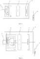
- FIG. 1 is a circuit diagram illustrating a charging circuit used in a mobile terminal in the related art.
- This charging circuit is known as BUCK circuit, which includes a MOS transistor, a control circuit, a diode, an inductor, and a battery.
- the control circuit controls the MOS transistor to turn-on and turn-off to generate a changing square wave current.
- the square wave current flows to the inductor from the MOS transistor, and then flows to the battery after voltage stabilization conducted by the inductor.
- the above mentioned charging process has a risk of MOS transistor breakdown.
- MOS transistor breakdown Upon MOS transistor breakdown, the current will flow through the inductor, a current/voltage detecting circuit, and the battery directly; this will cause the battery to exceed a limit voltage and may even lead to more serious consequences.
- the cause of the damage to the MOS transistor can be as follows.
- the MOS transistor is mis-energized; the voltage at both ends of the MOS transistor exceeds a maximum voltage that can be withstood; electrostatic breakdown or surge.
- the MOS transistor is of poor quality; or, there is an integrated manufacture technology issue.
- the value of on-resistance (RDSON) of the MOS transistor has been increased so as to improve the voltage resistance of the MOS transistor.
- high resistance in turn, would cause the charging circuit to be easy to heat, low energy transmission efficiency and so on.
- the present disclosure provides a charging circuit and a mobile terminal, with the aim of improving the reliability of a charging circuit in a mobile terminal.
- a charging circuit arranged between a charging interface and a battery of a mobile terminal, and includes: a first circuit, a capacitive coupling element, and a second circuit connected in series successively between the charging interface and the battery.
- the capacitive coupling element disconnects a direct-current (DC) path of the charging circuit.
- the first circuit includes a bridge-arm circuit and a control circuit controlling the bridge-arm circuit.
- the bridge-arm circuit connects with the charging interface, and is configured to charge/discharge capacitors in the capacitive coupling element under control of the control circuit, so as to convert DC, which is output from the charging interface and is used for charging, to AC.
- the second circuit is configured to adjust AC, which is coupled to the second circuit by the first circuit through the capacitive coupling element, to DC which is suitable for charging of the battery.
- the capacitive coupling element includes one capacitor
- the bridge-arm circuit is a half-bridge circuit including a first switch transistor and a second switch transistor.
- a first end of the first switch transistor connects with the charging interface, a second end of the first switch transistor connects with a first end of the capacitor, and a control end of the first switch transistor connects with the control circuit.
- a first end of the second switch transistor connects with the second end of the first switch transistor, a second end of the second switch transistor connects to ground, and a control end of the second switch transistor connects with the control circuit.
- a second end of the capacitor connects to ground via the second circuit.
- the capacitive coupling element includes a first capacitor and a second capacitor
- the bridge-arm circuit is a full-bridge circuit including a first switch transistor, a second switch transistor, a third switch transistor, and a fourth switch transistor.
- a first end of the first switch transistor connects with the charging interface
- a second end of the first switch transistor connects with a first end of the first capacitor
- a control end of the first switch transistor connects with the control circuit.
- a first end of the second switch transistor connects with the second end of the first switch transistor, a second end of the second switch transistor connects to ground, and a control end of the second switch transistor connects with the control circuit.
- a first end of the third switch transistor connects with the charging interface, a second end of the third switch transistor connects with a first end of the second capacitor, and a control end of the third switch transistor connects with the control circuit.
- a first end of the fourth switch transistor connects with the second end of the third switch transistor, a second end of the fourth switch transistor connects to ground, and a control end of the fourth switch transistor connects with the control circuit.
- a second end of the first capacitor connects with the second circuit; a second end of the second capacitor connects with the second circuit.
- the capacitors in the capacitive coupling element can be one of the following capacitors: a capacitor composed of printed circuit board (PCB); a capacitor composed of flexible printed circuit (FPC) board.
- PCB printed circuit board
- FPC flexible printed circuit
- the size, shape, or thickness of the capacitor in the capacitance coupling element is designed based on the structure of the mobile terminal.
- the bridge-arm circuit includes more than one metal oxide semiconductor field effect transistor (MOSFET).
- MOSFET metal oxide semiconductor field effect transistor
- the second circuit includes a rectifier circuit and a filter circuit.
- the mobile terminal includes a charging interface, a battery, and a charging interface according to the first aspect or any implementation of the first aspect.
- the charging circuit is arranged between the charging interface and the battery.
- the charging interface is a USB interface.
- the mobile terminal supports a normal charging mode and a quick charging mode, wherein charging current is larger in the quick charging mode than in the normal charging mode.
- a DC path of the charging circuit is separated by the capacitive coupling element. That is to say, there is no DC path in the charging circuit. DC current from the charging interface would not be output directly to the second circuit and the battery upon failure of the first circuit, whereby reliability of the charging circuit is improved.
- FIG. 2 is block schematic diagram illustrating a charging circuit according to an embodiment of the present disclosure.
- a charging circuit 30 is arranged between a charging interface 10 and a battery 20 of a terminal.
- the charging interface 30 includes a first circuit 31, a capacitive coupling element 33, and a second circuit 32 connected in series successively between the charging interface 10 and the battery 20.
- the capacitive coupling element 33 disconnects a direct-current (DC) path of the charging circuit 30.
- DC direct-current
- the first circuit 31 includes a bridge-arm circuit 312 and a control circuit 311 controlling the bridge-arm circuit.
- the bridge-arm circuit 312 connects with the charging interface 10, and is configured to charge/discharge capacitors in the capacitive coupling element 33 under control of the control circuit 311 so as to convert DC, which is output from the charging interface 10 and is used for charging, to AC.
- the second circuit 32 is configured to adjust alternating current (AC), which is coupled to the second circuit 32 by the first circuit 31 through the capacitive coupling element 33, to DC which is suitable for battery charging.
- AC alternating current
- a DC path of the charging circuit is separated by the capacitive coupling element. That is to say, there is no DC path in the charging circuit. DC current from the charging interface would not be output directly to the second circuit and the battery upon failure of the first circuit, whereby reliability of the charging circuit is improved.
- the capacitive coupling element 33 includes a capacitor C1
- the bridge-arm circuit is a half-bridge circuit including a first switch transistor T1 and a second switch transistor T2.
- a first end of the first switch transistor T1 connects with the charging interface 10
- a second end of the first switch transistor T2 connects with a first end of the capacitor C1
- a control end of the first switch transistor T1 connects with the control circuit 311.
- a first end of the second switch transistor T2 connects with the second end of the first switch transistor T1, a second end of the second switch transistor T2 connects to ground
- a control end of the second switch transistor T2 connects to the control circuit 311.
- a second end of the capacitor C1 connects to ground via the second circuit 32.
- the battery 20 connects to ground.
- a switch transistor (such as a MOS transistor), which is easy breakdown, is arranged within the first circuit.
- the first circuit could not convert DC to AC via the switch transistor; this cause DC input at the charging interface being applied to a subsequent component of the charging interface or a battery directly.
- a DC path of the charging circuit can be disconnected; therefore, AC is conducted while DC is blocked. That is to say, DC input at the charging interface cannot flow to the second circuit or the battery even if the switch transistor in the first circuit is broke down or failure, whereby the reliability of the charging circuit of the mobile terminal can be improved.
- the capacitive coupling element has good isolation performance.
- a lower on-resistance of the switch transistor in the first circuit is allowed, and this will improve the energy transfer efficiency of the whole charging circuit while reducing heating and loss.
- the capacitive coupling element 33 includes a first capacitor C1 and a second capacitor C2, and the bridge-arm circuit 312 is a full-bridge circuit including a first switch transistor T1, a second switch transistor T2, a third switch transistor T3, and a fourth switch transistor T4.
- a first end of the first switch transistor T1 connects with the charging interface 10
- a second end of the first switch transistor T1 connects with a first end of the first capacitor C1
- a control end of the first switch transistor T1 connects with the control circuit 311.
- a first end of the second switch transistor T2 connects with the second end of the first switch transistor T1, a second end of the second switch transistor T2 connects to ground, and a control end of the second switch transistor T2 connects with the control circuit 311.
- a first end of the third switch transistor T3 connects with the charging interface 10, a second end of the third switch transistor T3 connects with the first end of the second capacitor C2, and a control end of the third switch transistor T3 connects with the control circuit 311.
- a first end of the fourth switch transistor T4 connects with the second end of the third switch transistor T3, a second end of the fourth switch transistor T4 connects to ground, and a control end of the fourth switch transistor T4 connects with the control circuit 311.
- a second end of the first capacitor C1 connects with the second circuit 32; a second end of the second capacitor C2 connects with the second circuit 32.
- a switch transistor (such as a MOS transistor), which is easy breakdown, is arranged within the first circuit.
- the first circuit could not convert DC to AC via the switch transistor; this cause DC input at the charging interface being applied to a subsequent component of the charging interface or a battery directly.
- a DC path of the charging circuit can be disconnected; therefore, AC is conducted while DC is blocked. That is to say, DC input at the charging interface cannot flow to the second circuit or the battery even if the switch transistor in the first circuit is broke down or failure, whereby the reliability of the charging circuit of the mobile terminal can be improved.
- the capacitive coupling element has good isolation performance.
- a lower on-resistance of the switch transistor in the first circuit is allowed, and this will improve the energy transfer efficiency of the whole charging circuit while reducing heating and loss.
- the capacitor in the capacitive coupling element 33 can be one of the following capacitors: a capacitor composed of printed circuit board (PCB); a capacitor composed of flexible printed circuit (FPC) board.
- PCB printed circuit board
- FPC flexible printed circuit
- the capacitor composed of PCB can be a capacitor composed of PCB sheets and copper foil on the sheets.
- the capacitor composed of FPC board can be a capacitor composed and designed by FPC.
- the main advantage of the capacitor composed of PCB and the capacitor composed of FPC board lies in that, the capacitor can be designed arbitrarily to have any shape, any size, or any thickness, according to the structure and shape of the mobile terminal such as a smart phone.
- the size, shape, or thickness of the capacitor in the capacitance coupling element is designed based on the structure of the mobile terminal.
- the bridge-arm circuit includes more than one metal oxide semiconductor field effect transistor (MOSFET).
- MOSFET metal oxide semiconductor field effect transistor
- the second circuit includes a rectifier circuit and a filter circuit.
- FIG. 5 is a block schematic diagram illustrating a mobile terminal according to an embodiment of the present disclosure.
- a mobile terminal 50 includes a charging interface 51, a battery 52, and a charging circuit 53.
- the charging circuit 53 can adopt any of the implementations of the charging circuit 30 described above.
- a DC path of the charging circuit is separated by the capacitive coupling element. That is to say, there is no DC path in the charging circuit. DC current from the charging interface would not be output directly to the second circuit and the battery upon failure of the first circuit, whereby reliability of the charging circuit is improved.
- the charging interface 51 is a USB interface.
- the mobile terminal 50 supports a normal charging mode and a quick charging mode, wherein charging current is larger in the quick charging mode than in the normal charging mode.
- the phenomenon of MOS transistor breakdown is particularly serious in the mobile terminal which supports quick charging.
- the mobile terminal according to the embodiment of the present disclosure can be a good solution.
- the device, system, and method described herein can be achieved in other manners.
- the configuration of the device according to the embodiment described above is only exemplary; the division of units in the device is a kind of division according to logical function, therefore there can be other divisions in practice.
- multiple units or components can be combined or integrated into another system; or, some features can be ignored while some units need not to be executed.
- various function units can be integrated into one processing unit; two or more than two units can be integrated into one unit; or, each unit is physically separate.
- various function units can be integrated into one processing unit; two or more than two units can be integrated into one unit; or, each unit is physically separate.
- Operations or functions of technical schemes according to the embodiments of the present disclosure when achieved in the form of software functional units and sold or used as an independent product, can be stored in a computer readable storage medium.
- a computer readable storage medium includes USB disk, Read Only Memory (ROM), Random Access Memory (RAM), magnetic disk, CD, and any other medium that can be configured to store computer-readable program code or instructions.
- the computer-readable program code when executed on a data-processing apparatus (can be personal computer, server, or network equipment), adapted to perform all or a part of the methods described in the above-mentioned embodiments.
Landscapes
- Engineering & Computer Science (AREA)
- Power Engineering (AREA)
- Charge And Discharge Circuits For Batteries Or The Like (AREA)
- Telephone Function (AREA)
- Power Sources (AREA)
Abstract
Description
- The present disclosure relates to mobile terminal field, and particularly to a charging circuit and a mobile terminal.
- With the growing popularity of mobile terminal use, terminal charging has become a focused issue of mobile terminal providers.
-
FIG. 1 is a circuit diagram illustrating a charging circuit used in a mobile terminal in the related art. This charging circuit is known as BUCK circuit, which includes a MOS transistor, a control circuit, a diode, an inductor, and a battery. Upon charging, the control circuit controls the MOS transistor to turn-on and turn-off to generate a changing square wave current. The square wave current flows to the inductor from the MOS transistor, and then flows to the battery after voltage stabilization conducted by the inductor. - The above mentioned charging process has a risk of MOS transistor breakdown. Upon MOS transistor breakdown, the current will flow through the inductor, a current/voltage detecting circuit, and the battery directly; this will cause the battery to exceed a limit voltage and may even lead to more serious consequences.
- The cause of the damage to the MOS transistor can be as follows.
- The MOS transistor is mis-energized; the voltage at both ends of the MOS transistor exceeds a maximum voltage that can be withstood; electrostatic breakdown or surge.
- The MOS transistor is of poor quality; or, there is an integrated manufacture technology issue.
- There can be other defects.
- In order to avoid the above problems and improve the reliability of the MOS transistor, the value of on-resistance (RDSON) of the MOS transistor has been increased so as to improve the voltage resistance of the MOS transistor. On the other hand, high resistance, in turn, would cause the charging circuit to be easy to heat, low energy transmission efficiency and so on.
- The present disclosure provides a charging circuit and a mobile terminal, with the aim of improving the reliability of a charging circuit in a mobile terminal.
- According to a first aspect, it is provided a charging circuit. The charging circuit arranged between a charging interface and a battery of a mobile terminal, and includes: a first circuit, a capacitive coupling element, and a second circuit connected in series successively between the charging interface and the battery. The capacitive coupling element disconnects a direct-current (DC) path of the charging circuit. The first circuit includes a bridge-arm circuit and a control circuit controlling the bridge-arm circuit. The bridge-arm circuit connects with the charging interface, and is configured to charge/discharge capacitors in the capacitive coupling element under control of the control circuit, so as to convert DC, which is output from the charging interface and is used for charging, to AC. The second circuit is configured to adjust AC, which is coupled to the second circuit by the first circuit through the capacitive coupling element, to DC which is suitable for charging of the battery.
- Based on the first aspect, in one implementation, the capacitive coupling element includes one capacitor, and the bridge-arm circuit is a half-bridge circuit including a first switch transistor and a second switch transistor. A first end of the first switch transistor connects with the charging interface, a second end of the first switch transistor connects with a first end of the capacitor, and a control end of the first switch transistor connects with the control circuit. A first end of the second switch transistor connects with the second end of the first switch transistor, a second end of the second switch transistor connects to ground, and a control end of the second switch transistor connects with the control circuit. A second end of the capacitor connects to ground via the second circuit.
- Based on the first aspect or any of the above implementations, in another implementation, the capacitive coupling element includes a first capacitor and a second capacitor, and the bridge-arm circuit is a full-bridge circuit including a first switch transistor, a second switch transistor, a third switch transistor, and a fourth switch transistor. A first end of the first switch transistor connects with the charging interface, a second end of the first switch transistor connects with a first end of the first capacitor, and a control end of the first switch transistor connects with the control circuit. A first end of the second switch transistor connects with the second end of the first switch transistor, a second end of the second switch transistor connects to ground, and a control end of the second switch transistor connects with the control circuit. A first end of the third switch transistor connects with the charging interface, a second end of the third switch transistor connects with a first end of the second capacitor, and a control end of the third switch transistor connects with the control circuit. A first end of the fourth switch transistor connects with the second end of the third switch transistor, a second end of the fourth switch transistor connects to ground, and a control end of the fourth switch transistor connects with the control circuit. A second end of the first capacitor connects with the second circuit; a second end of the second capacitor connects with the second circuit.
- Based on the first aspect or any of the above implementations, in another implementation, the capacitors in the capacitive coupling element can be one of the following capacitors: a capacitor composed of printed circuit board (PCB); a capacitor composed of flexible printed circuit (FPC) board.
- Based on the first aspect or any of the above implementations, in another implementation, the size, shape, or thickness of the capacitor in the capacitance coupling element is designed based on the structure of the mobile terminal.
- Based on the first aspect or any of the above implementations, in another implementation, the bridge-arm circuit includes more than one metal oxide semiconductor field effect transistor (MOSFET).
- Based on the first aspect or any of the above implementations, in another implementation, the second circuit includes a rectifier circuit and a filter circuit.
- According to a second aspect of the present disclosure, it is provided mobile terminal. The mobile terminal includes a charging interface, a battery, and a charging interface according to the first aspect or any implementation of the first aspect. The charging circuit is arranged between the charging interface and the battery.
- Based on the second aspect, in one implementation, the charging interface is a USB interface.
- Based on the second aspect or any of the above implementations, in one implementation, the mobile terminal supports a normal charging mode and a quick charging mode, wherein charging current is larger in the quick charging mode than in the normal charging mode.
- In the technical schemes described above, a DC path of the charging circuit is separated by the capacitive coupling element. That is to say, there is no DC path in the charging circuit. DC current from the charging interface would not be output directly to the second circuit and the battery upon failure of the first circuit, whereby reliability of the charging circuit is improved.
- In order to illustrate the technical solutions of the present disclosure or the related art more clearly, a brief description of the accompanying drawings used herein is given below. Obviously, the drawings listed below are only examples, and a person skilled in the art should be noted that, other drawings can also be obtained on the basis of these exemplary drawings without creative work.
-
FIG. 1 is a circuit diagram illustrating a charging circuit in the related art. -
FIG. 2 is a block schematic diagram illustrating a charging circuit according to an embodiment of the present disclosure. -
FIG. 3 is a circuit diagram illustrating a charging circuit according to an embodiment of the present disclosure. -
FIG. 4 is a circuit diagram illustrating a charging circuit according to an embodiment of the present disclosure. -
FIG. 5 is a block schematic diagram illustrating a mobile terminal according to an embodiment of the present disclosure. - Technical solutions of the embodiments of the present disclosure will be described clearly and completely taken in conjunction with the accompanying drawings; it will be apparent to one of ordinary skill in the art that, the embodiments described below are merely a part of the disclosure and other embodiments obtained out of them without creative work will fall into the protection range of the present disclosure either.
-
FIG. 2 is block schematic diagram illustrating a charging circuit according to an embodiment of the present disclosure. As shown inFIG.2 , acharging circuit 30 is arranged between acharging interface 10 and abattery 20 of a terminal. Thecharging interface 30 includes afirst circuit 31, acapacitive coupling element 33, and asecond circuit 32 connected in series successively between thecharging interface 10 and the battery 20.Thecapacitive coupling element 33 disconnects a direct-current (DC) path of thecharging circuit 30. - Specifically, the
first circuit 31 includes a bridge-arm circuit 312 and acontrol circuit 311 controlling the bridge-arm circuit. The bridge-arm circuit 312 connects with thecharging interface 10, and is configured to charge/discharge capacitors in thecapacitive coupling element 33 under control of thecontrol circuit 311 so as to convert DC, which is output from thecharging interface 10 and is used for charging, to AC. - The
second circuit 32 is configured to adjust alternating current (AC), which is coupled to thesecond circuit 32 by thefirst circuit 31 through thecapacitive coupling element 33, to DC which is suitable for battery charging. - In this technical scheme, a DC path of the charging circuit is separated by the capacitive coupling element. That is to say, there is no DC path in the charging circuit. DC current from the charging interface would not be output directly to the second circuit and the battery upon failure of the first circuit, whereby reliability of the charging circuit is improved.
- As an embodiment, as shown in
FIG.3 , thecapacitive coupling element 33 includes a capacitor C1, and the bridge-arm circuit is a half-bridge circuit including a first switch transistor T1 and a second switch transistor T2. A first end of the first switch transistor T1 connects with the charginginterface 10, a second end of the first switch transistor T2 connects with a first end of the capacitor C1, and a control end of the first switch transistor T1 connects with thecontrol circuit 311. A first end of the second switch transistor T2 connects with the second end of the first switch transistor T1, a second end of the second switch transistor T2 connects to ground, and a control end of the second switch transistor T2 connects to thecontrol circuit 311. A second end of the capacitor C1 connects to ground via thesecond circuit 32. Thebattery 20 connects to ground. - In the embodiment of the present disclosure, a switch transistor (such as a MOS transistor), which is easy breakdown, is arranged within the first circuit. When breakdown of the switch transistor occurs, the first circuit could not convert DC to AC via the switch transistor; this cause DC input at the charging interface being applied to a subsequent component of the charging interface or a battery directly. However, with the aid of the capacitive coupling element arranged between the first circuit and the second circuit, a DC path of the charging circuit can be disconnected; therefore, AC is conducted while DC is blocked. That is to say, DC input at the charging interface cannot flow to the second circuit or the battery even if the switch transistor in the first circuit is broke down or failure, whereby the reliability of the charging circuit of the mobile terminal can be improved.
- In addition, the capacitive coupling element has good isolation performance. Thus, instead of increasing the on-resistance so as to increase the voltage resistance of the MOS transistor and then improve the reliability of the circuit like in the prior art, in embodiments of the present disclosure, a lower on-resistance of the switch transistor in the first circuit is allowed, and this will improve the energy transfer efficiency of the whole charging circuit while reducing heating and loss.
- As an embodiment, the
capacitive coupling element 33 includes a first capacitor C1 and a second capacitor C2, and the bridge-arm circuit 312 is a full-bridge circuit including a first switch transistor T1, a second switch transistor T2, a third switch transistor T3, and a fourth switch transistor T4. A first end of the first switch transistor T1 connects with the charginginterface 10, a second end of the first switch transistor T1 connects with a first end of the first capacitor C1, and a control end of the first switch transistor T1 connects with thecontrol circuit 311. A first end of the second switch transistor T2 connects with the second end of the first switch transistor T1, a second end of the second switch transistor T2 connects to ground, and a control end of the second switch transistor T2 connects with thecontrol circuit 311. A first end of the third switch transistor T3 connects with the charginginterface 10, a second end of the third switch transistor T3 connects with the first end of the second capacitor C2, and a control end of the third switch transistor T3 connects with thecontrol circuit 311. A first end of the fourth switch transistor T4 connects with the second end of the third switch transistor T3, a second end of the fourth switch transistor T4 connects to ground, and a control end of the fourth switch transistor T4 connects with thecontrol circuit 311. A second end of the first capacitor C1 connects with thesecond circuit 32; a second end of the second capacitor C2 connects with thesecond circuit 32. - In the embodiment of the present disclosure, a switch transistor (such as a MOS transistor), which is easy breakdown, is arranged within the first circuit. When breakdown of the switch transistor occurs, the first circuit could not convert DC to AC via the switch transistor; this cause DC input at the charging interface being applied to a subsequent component of the charging interface or a battery directly. However, with the aid of the capacitive coupling element arranged between the first circuit and the second circuit, a DC path of the charging circuit can be disconnected; therefore, AC is conducted while DC is blocked. That is to say, DC input at the charging interface cannot flow to the second circuit or the battery even if the switch transistor in the first circuit is broke down or failure, whereby the reliability of the charging circuit of the mobile terminal can be improved.
- In addition, the capacitive coupling element has good isolation performance. Thus, instead of increasing the on-resistance so as to increase the voltage resistance of the MOS transistor and then improve the reliability of the circuit like in the prior art, in embodiments of the present disclosure, a lower on-resistance of the switch transistor in the first circuit is allowed, and this will improve the energy transfer efficiency of the whole charging circuit while reducing heating and loss.
- The capacitor in the
capacitive coupling element 33 can be one of the following capacitors: a capacitor composed of printed circuit board (PCB); a capacitor composed of flexible printed circuit (FPC) board. - Specifically, the capacitor composed of PCB can be a capacitor composed of PCB sheets and copper foil on the sheets. The capacitor composed of FPC board can be a capacitor composed and designed by FPC. The main advantage of the capacitor composed of PCB and the capacitor composed of FPC board lies in that, the capacitor can be designed arbitrarily to have any shape, any size, or any thickness, according to the structure and shape of the mobile terminal such as a smart phone.
- As an embodiment, the size, shape, or thickness of the capacitor in the capacitance coupling element is designed based on the structure of the mobile terminal.
- As an embodiment, the bridge-arm circuit includes more than one metal oxide semiconductor field effect transistor (MOSFET).
- As an embodiment, the second circuit includes a rectifier circuit and a filter circuit.
-
FIG. 5 is a block schematic diagram illustrating a mobile terminal according to an embodiment of the present disclosure. As shown inFIG. 5 , amobile terminal 50 includes a charginginterface 51, abattery 52, and a chargingcircuit 53. The chargingcircuit 53 can adopt any of the implementations of the chargingcircuit 30 described above. - In the technical scheme described above, a DC path of the charging circuit is separated by the capacitive coupling element. That is to say, there is no DC path in the charging circuit. DC current from the charging interface would not be output directly to the second circuit and the battery upon failure of the first circuit, whereby reliability of the charging circuit is improved.
- As an embodiment, the charging
interface 51 is a USB interface. - As an embodiment, the
mobile terminal 50 supports a normal charging mode and a quick charging mode, wherein charging current is larger in the quick charging mode than in the normal charging mode. - It should be understood that the phenomenon of MOS transistor breakdown is particularly serious in the mobile terminal which supports quick charging. As to the problem of circuit unreliability upon quick charging caused by MOS transistor breakdown, the mobile terminal according to the embodiment of the present disclosure can be a good solution.
- A person skilled in the art will understand, exemplary units or algorithm steps described in any of the embodiments can be achieved via electronic hardware or a combination of electronic hardware and computer software. Whether hardware or software should be adopted depends on design constraints and specific applications of the technical schemes. Respective specific application can use different methods or manners to achieve the function described in the embodiments, which will fall into the protection scope of the present disclosure.
- Specific operations of the device, system, and the unit or module can refer to corresponding description of the method according to the embodiment, and will not go into much detail here.
- In the embodiments of the present disclosure, the device, system, and method described herein can be achieved in other manners. The configuration of the device according to the embodiment described above is only exemplary; the division of units in the device is a kind of division according to logical function, therefore there can be other divisions in practice. For example, multiple units or components can be combined or integrated into another system; or, some features can be ignored while some units need not to be executed. On the other hand, various function units can be integrated into one processing unit; two or more than two units can be integrated into one unit; or, each unit is physically separate.
- Furthermore, various function units can be integrated into one processing unit; two or more than two units can be integrated into one unit; or, each unit is physically separate.
- Operations or functions of technical schemes according to the embodiments of the present disclosure, when achieved in the form of software functional units and sold or used as an independent product, can be stored in a computer readable storage medium. According to this, all or a part of the technical schemes of the present disclosure can be realized in the form of software products which can be stored in a storage medium. The storage medium includes USB disk, Read Only Memory (ROM), Random Access Memory (RAM), magnetic disk, CD, and any other medium that can be configured to store computer-readable program code or instructions. The computer-readable program code, when executed on a data-processing apparatus (can be personal computer, server, or network equipment), adapted to perform all or a part of the methods described in the above-mentioned embodiments.
- The foregoing descriptions are merely preferred embodiments of the present disclosure, rather than limiting the present disclosure. Various modifications and alterations may be made to the present disclosure for those skilled in the art. Any modification, equivalent substitution, improvement or the like made within the spirit and principle of the present disclosure shall fall into the protection scope of the present disclosure.
Claims (10)
- A charging circuit, being configured to be arranged between a charging interface and a battery of a mobile terminal, and comprising: a first circuit, a capacitive coupling element, and a second circuit connected in series successively between the charging interface and the battery, a direct-current, DC, path of the charging circuit being disconnected by the capacitive coupling element; wherein
the first circuit comprises a bridge-arm circuit and a control circuit controlling the bridge-arm circuit; the bridge-arm circuit is configured to connect with the charging interface and charge/discharge capacitors in the capacitive coupling element under control of the control circuit, so as to convert DC, which is output from the charging interface and is used for charging, to alternating current, AC; and
the second circuit is configured to adjust AC, which is coupled to the second circuit by the first circuit through the capacitive coupling element, to DC which is suitable for charging of the battery. - The charging circuit of claim 1, wherein the capacitive coupling element comprises one capacitor, and the bridge-arm circuit is a half-bridge circuit comprising a first switch transistor and a second switch transistor; wherein
the first switch transistor has a first end configured to connect with the charging interface, a second end connected with a first end of the capacitor, and a control end connected with the control circuit;
the second switch transistor has a first end connected with the second end of the first switch transistor, a second end configured to connect to ground, and a control end connected with the control circuit; and
the capacitor has a second end configured to connect to ground via the second circuit and the battery. - The charging circuit of claim 1, wherein the capacitive coupling element comprises a first capacitor and a second capacitor, and the bridge-arm circuit is a full-bridge circuit comprising a first switch transistor, a second switch transistor, a third switch transistor, and a fourth switch transistor; wherein
the first switch transistor has a first end configured to connect with the charging interface, a second end connected with a first end of the first capacitor, and a control end connected with the control circuit;
the second switch transistor has a first end connected with the second end of the first switch transistor, a second end configured to connect to ground, and a control end connected with the control circuit;
the third switch transistor has a first end configured to connect with the charging interface, a second end connected with a first end of the second capacitor, and a control end connected with the control circuit;
the fourth switch transistor has a first end connected with the second end of the third switch transistor, a second end configured to connect to ground, and a control end connected with the control circuit;
the first capacitor has a second end connected with the second circuit; and
the second capacitor has a second end connected with the second circuit. - The charging circuit of claim 1, wherein the capacitors in the capacitive coupling element can be one of the following capacitors: a capacitor composed of printed circuit board (PCB); a capacitor composed of flexible printed circuit (FPC) board.
- The charging circuit of any of claims 1-4, a size, shape, or thickness of the capacitors in the capacitance coupling element is designed based on the structure of the mobile terminal.
- The charging circuit of any of claims 1-5, wherein the bridge-arm circuit comprises more than one metal oxide semiconductor field effect transistor (MOSFET).
- The charging circuit of any of claims 1-6, wherein the second circuit comprises a rectifier circuit and a filter circuit.
- A mobile terminal, comprising a charging interface, a battery, and a charging circuit according to any of claims 1-7; the charging circuit is arranged between the charging interface and the battery.
- The mobile terminal of claim 8, wherein the charging interface is a USB interface.
- The mobile terminal of claim 8 or 9, wherein the mobile terminal supports a normal charging mode and a quick charging mode; charging current is larger in the quick charging mode than in the normal charging mode.
Applications Claiming Priority (1)
| Application Number | Priority Date | Filing Date | Title |
|---|---|---|---|
| PCT/CN2015/080499 WO2016192010A1 (en) | 2015-06-01 | 2015-06-01 | Charging circuit and mobile terminal |
Publications (3)
| Publication Number | Publication Date |
|---|---|
| EP3148040A1 true EP3148040A1 (en) | 2017-03-29 |
| EP3148040A4 EP3148040A4 (en) | 2018-05-30 |
| EP3148040B1 EP3148040B1 (en) | 2023-08-16 |
Family
ID=56744380
Family Applications (1)
| Application Number | Title | Priority Date | Filing Date |
|---|---|---|---|
| EP15893543.7A Active EP3148040B1 (en) | 2015-06-01 | 2015-06-01 | Charging circuit and mobile terminal |
Country Status (14)
| Country | Link |
|---|---|
| US (2) | US20170085105A1 (en) |
| EP (1) | EP3148040B1 (en) |
| JP (1) | JP2017529044A (en) |
| KR (1) | KR101927645B1 (en) |
| CN (2) | CN105917546B (en) |
| AU (1) | AU2015397728B2 (en) |
| BR (1) | BR112017006275A2 (en) |
| CA (1) | CA2960423C (en) |
| MX (1) | MX364315B (en) |
| MY (1) | MY192075A (en) |
| PH (1) | PH12017500897A1 (en) |
| SG (1) | SG11201701765RA (en) |
| TW (2) | TWI646751B (en) |
| WO (1) | WO2016192010A1 (en) |
Families Citing this family (8)
| Publication number | Priority date | Publication date | Assignee | Title |
|---|---|---|---|---|
| CN105917546B (en) * | 2015-06-01 | 2018-02-02 | 广东欧珀移动通信有限公司 | Charging circuit and mobile terminal |
| CN106891744B (en) * | 2015-12-18 | 2019-11-08 | 比亚迪股份有限公司 | Electric vehicle and its on-board charger and control method of on-board charger |
| CN106891748B (en) * | 2015-12-18 | 2019-02-26 | 比亚迪股份有限公司 | Electric vehicle and its on-board charger and control method of on-board charger |
| CN209488195U (en) | 2016-10-12 | 2019-10-11 | Oppo广东移动通信有限公司 | Mobile terminal |
| CN107995770B (en) * | 2017-11-10 | 2021-04-02 | 惠科股份有限公司 | Flexible flat cable and display panel |
| CN109889278A (en) * | 2019-02-20 | 2019-06-14 | 维沃移动通信有限公司 | Mobile terminal and the method for improving speech quality |
| WO2020227921A1 (en) | 2019-05-14 | 2020-11-19 | Oppo广东移动通信有限公司 | Step-down circuit, electronic device, and step-down method |
| JP7446390B2 (en) * | 2021-11-08 | 2024-03-08 | 台達電子工業股▲ふん▼有限公司 | Integrated power system with motor drive and battery charging/discharging |
Family Cites Families (55)
| Publication number | Priority date | Publication date | Assignee | Title |
|---|---|---|---|---|
| JPS502119A (en) * | 1973-05-15 | 1975-01-10 | ||
| GB2147159B (en) * | 1983-09-19 | 1987-06-10 | Minitronics Pty Ltd | Power converter |
| US4858071A (en) * | 1987-02-24 | 1989-08-15 | Nissan Motor Co., Ltd. | Electronic circuit apparatus |
| EP0398722A3 (en) * | 1989-05-18 | 1991-01-30 | Hirotami Nakano | Uninterruptable power supply apparatus and isolating method thereof |
| US5045768A (en) * | 1989-10-27 | 1991-09-03 | International Rectifier Corporation | Off-line battery charger |
| ATE403240T1 (en) * | 1997-01-03 | 2008-08-15 | Schleifring Und Appbau Gmbh | DEVICE FOR THE CONTACTLESS TRANSMISSION OF ELECTRICAL SIGNALS AND/OR ENERGY |
| US5892351A (en) * | 1997-08-29 | 1999-04-06 | Compaq Computer Corporation | DC-isolated converting battery module |
| JP3201603B1 (en) * | 1999-06-30 | 2001-08-27 | 富士通株式会社 | Driving device, driving method, and driving circuit for plasma display panel |
| AU6335400A (en) * | 1999-07-02 | 2001-01-22 | Fusion Lighting, Inc. | High output lamp with high brightness |
| JP4284806B2 (en) * | 2000-01-31 | 2009-06-24 | パナソニック電工株式会社 | Power supply |
| JP2001357867A (en) * | 2000-06-12 | 2001-12-26 | Matsushita Electric Ind Co Ltd | Fuel cell power generator, medium and information aggregate |
| US6462962B1 (en) * | 2000-09-08 | 2002-10-08 | Slobodan Cuk | Lossless switching DC-to-DC converter |
| US6362979B1 (en) * | 2000-09-29 | 2002-03-26 | Jeff Gucyski | Switching power amplifier and uninterruptible power system comprising DC/DC converter for providing sinusoidal output |
| US6385056B1 (en) * | 2000-09-29 | 2002-05-07 | Jeff Gucyski | Precision switching power amplifier and uninterruptible power system |
| CA2369060C (en) * | 2001-01-24 | 2005-10-04 | Nissin Electric Co., Ltd. | Dc-dc-converter and bi-directional dc-dc converter and method of controlling the same |
| US7528643B2 (en) * | 2003-02-12 | 2009-05-05 | Semiconductor Energy Laboratory Co., Ltd. | Semiconductor device, electronic device having the same, and driving method of the same |
| TWI255572B (en) * | 2004-05-05 | 2006-05-21 | Advanced Connectek Inc | A portable electrical power unit with transmission display |
| DE102004031216A1 (en) * | 2004-06-28 | 2006-01-19 | Siemens Ag | Apparatus and method for charge equalization in series connected energy storage |
| DE102005014285A1 (en) * | 2005-03-24 | 2006-10-05 | Siemens Ag | Apparatus and method for charge equalization of arranged in series individual cells of an energy storage |
| DE102005030601A1 (en) * | 2005-06-30 | 2007-01-11 | Siemens Ag Österreich | Power supply with full bridge circuit and large control range |
| US20080186004A1 (en) * | 2005-11-29 | 2008-08-07 | Advanced Analogic Technologies, Inc. | High-Frequency Power MESFET Boost Switching Power Supply |
| TW200742491A (en) * | 2006-04-17 | 2007-11-01 | Delta Electronics Inc | Power supply system for lighting lamp |
| JP2007322182A (en) * | 2006-05-30 | 2007-12-13 | Kyocera Corp | Electronic device and portable terminal device |
| GB0623653D0 (en) * | 2006-11-27 | 2007-01-03 | Innovision Res & Tech Plc | Near field RF communicators and near field RF communications enabled devices |
| US7982332B2 (en) * | 2006-12-08 | 2011-07-19 | Chrysler Group Llc | Power device for a vehicle |
| JP2008187821A (en) * | 2007-01-30 | 2008-08-14 | Matsushita Electric Works Ltd | Insulated ac-dc converter and dc power supply unit for led using it |
| US7620151B2 (en) * | 2007-08-07 | 2009-11-17 | General Electric Co | High voltage tank assembly for radiation generator |
| WO2009070171A1 (en) * | 2007-11-30 | 2009-06-04 | Agere Systems Inc. | Power sharing among portable electronic devices |
| CN102210080B (en) * | 2008-09-08 | 2015-06-03 | 创科电动工具科技有限公司 | Battery charger |
| CN103166467B (en) * | 2011-12-09 | 2015-10-21 | 台达电子企业管理(上海)有限公司 | A kind of converter circuit and method with input voltage balancing circuitry |
| EP2296156A1 (en) * | 2009-08-13 | 2011-03-16 | ABB Research Ltd | Composite capacitance and use thereof |
| JP2012019382A (en) * | 2010-07-08 | 2012-01-26 | Sony Corp | Electronic apparatus |
| KR101664971B1 (en) * | 2010-08-18 | 2016-10-11 | 핀식스 코포레이션 | Ultra-High-Frequency Switching Cell-Based Power Converters |
| JP2012054637A (en) * | 2010-08-31 | 2012-03-15 | Ntt Docomo Inc | Charger and portable terminal |
| US8558584B2 (en) * | 2010-11-30 | 2013-10-15 | Infineon Technologies Ag | System and method for bootstrapping a switch driver |
| CN201928063U (en) * | 2010-12-10 | 2011-08-10 | 广州锐研机电设备有限公司 | Charging circuit for resistance welder |
| TWM416006U (en) * | 2011-01-12 | 2011-11-11 | Logah Technology Corp | Wireless energy lighting device |
| US20120262967A1 (en) * | 2011-04-13 | 2012-10-18 | Cuks, Llc | Single-stage inverter with high frequency isolation transformer |
| JP5802073B2 (en) * | 2011-07-26 | 2015-10-28 | パナソニック株式会社 | Bidirectional power converter |
| US8981749B2 (en) * | 2011-10-12 | 2015-03-17 | Blackberry Limited | Power converter system for mobile devices |
| JP5997456B2 (en) * | 2012-02-17 | 2016-09-28 | 学校法人慶應義塾 | Wireless power feeder |
| JP6136025B2 (en) * | 2012-03-15 | 2017-05-31 | パナソニックIpマネジメント株式会社 | Non-contact charging device power supply device |
| ITRE20120021A1 (en) * | 2012-04-02 | 2013-10-03 | Igor Spinella | METHOD AND APPARATUS FOR ELECTRIC POWER TRANSFER |
| KR101473890B1 (en) * | 2012-04-09 | 2014-12-24 | 김창호 | Power supply system cutting off standby electric power |
| US9599524B2 (en) * | 2013-04-04 | 2017-03-21 | University Of Utah Research Foundation | High-resolution flexible tactile imager system based on floating comb electrode |
| JP2015056933A (en) * | 2013-09-11 | 2015-03-23 | 三菱電機株式会社 | Power conversion apparatus |
| CN104578439B (en) * | 2013-10-21 | 2018-10-09 | 台达电子企业管理(上海)有限公司 | Device for wireless charging link |
| EP3084946A2 (en) * | 2013-12-18 | 2016-10-26 | Danmarks Tekniske Universitet | Step-up dc-dc power converter |
| GB2524102A (en) * | 2014-03-14 | 2015-09-16 | Eisergy Ltd | A switched mode AC-DC converter |
| JP2016123258A (en) * | 2014-06-02 | 2016-07-07 | パナソニックIpマネジメント株式会社 | Switching power supply and charging device |
| US9537400B2 (en) * | 2014-08-29 | 2017-01-03 | Infineon Technologies Austria Ag | Switching converter with dead time between switching of switches |
| JP6102872B2 (en) * | 2014-09-25 | 2017-03-29 | 株式会社豊田中央研究所 | Power converter |
| KR102051943B1 (en) * | 2015-06-01 | 2019-12-04 | 광동 오포 모바일 텔레커뮤니케이션즈 코포레이션 리미티드 | Charging circuit and mobile terminal |
| CN105917546B (en) * | 2015-06-01 | 2018-02-02 | 广东欧珀移动通信有限公司 | Charging circuit and mobile terminal |
| CN109861356B (en) * | 2018-05-09 | 2023-03-24 | 台达电子工业股份有限公司 | Impact current suppression module, vehicle-mounted bidirectional charger and control method |
-
2015
- 2015-06-01 CN CN201580004531.0A patent/CN105917546B/en active Active
- 2015-06-01 CA CA2960423A patent/CA2960423C/en active Active
- 2015-06-01 WO PCT/CN2015/080499 patent/WO2016192010A1/en not_active Ceased
- 2015-06-01 EP EP15893543.7A patent/EP3148040B1/en active Active
- 2015-06-01 BR BR112017006275A patent/BR112017006275A2/en not_active Application Discontinuation
- 2015-06-01 JP JP2017513193A patent/JP2017529044A/en active Pending
- 2015-06-01 MY MYPI2017000629A patent/MY192075A/en unknown
- 2015-06-01 SG SG11201701765RA patent/SG11201701765RA/en unknown
- 2015-06-01 CN CN201711329821.XA patent/CN107979134A/en active Pending
- 2015-06-01 KR KR1020177006322A patent/KR101927645B1/en not_active Expired - Fee Related
- 2015-06-01 MX MX2017004066A patent/MX364315B/en active IP Right Grant
- 2015-06-01 AU AU2015397728A patent/AU2015397728B2/en not_active Ceased
-
2016
- 2016-05-31 TW TW105117064A patent/TWI646751B/en not_active IP Right Cessation
- 2016-05-31 TW TW107116855A patent/TWI646756B/en not_active IP Right Cessation
- 2016-12-07 US US15/371,456 patent/US20170085105A1/en not_active Abandoned
-
2017
- 2017-05-15 PH PH12017500897A patent/PH12017500897A1/en unknown
-
2018
- 2018-05-24 US US15/989,040 patent/US20180278069A1/en not_active Abandoned
Also Published As
| Publication number | Publication date |
|---|---|
| PH12017500897A1 (en) | 2017-11-06 |
| CN105917546A (en) | 2016-08-31 |
| JP2017529044A (en) | 2017-09-28 |
| MY192075A (en) | 2022-07-26 |
| WO2016192010A1 (en) | 2016-12-08 |
| TWI646751B (en) | 2019-01-01 |
| BR112017006275A2 (en) | 2017-12-12 |
| CA2960423C (en) | 2019-01-22 |
| EP3148040A4 (en) | 2018-05-30 |
| KR20170041822A (en) | 2017-04-17 |
| CN107979134A (en) | 2018-05-01 |
| US20180278069A1 (en) | 2018-09-27 |
| CA2960423A1 (en) | 2016-12-08 |
| TWI646756B (en) | 2019-01-01 |
| TW201703385A (en) | 2017-01-16 |
| KR101927645B1 (en) | 2019-03-12 |
| TW201832445A (en) | 2018-09-01 |
| AU2015397728A1 (en) | 2017-03-30 |
| SG11201701765RA (en) | 2017-12-28 |
| CN105917546B (en) | 2018-02-02 |
| MX364315B (en) | 2019-04-22 |
| US20170085105A1 (en) | 2017-03-23 |
| EP3148040B1 (en) | 2023-08-16 |
| MX2017004066A (en) | 2017-06-12 |
| AU2015397728B2 (en) | 2018-08-30 |
Similar Documents
| Publication | Publication Date | Title |
|---|---|---|
| CA2960423C (en) | Charging circuit and mobile terminal | |
| CA2960419C (en) | Charging circuit and mobile terminal | |
| US9281758B1 (en) | Constant inrush current circuit for AC input power supply unit | |
| CN109888895B (en) | Charging circuit and mobile terminal | |
| JP6976982B2 (en) | Charging circuit and mobile terminal | |
| CN108512410A (en) | A kind of AC power soft starting device |
Legal Events
| Date | Code | Title | Description |
|---|---|---|---|
| STAA | Information on the status of an ep patent application or granted ep patent |
Free format text: STATUS: UNKNOWN |
|
| STAA | Information on the status of an ep patent application or granted ep patent |
Free format text: STATUS: THE INTERNATIONAL PUBLICATION HAS BEEN MADE |
|
| PUAI | Public reference made under article 153(3) epc to a published international application that has entered the european phase |
Free format text: ORIGINAL CODE: 0009012 |
|
| STAA | Information on the status of an ep patent application or granted ep patent |
Free format text: STATUS: REQUEST FOR EXAMINATION WAS MADE |
|
| 17P | Request for examination filed |
Effective date: 20161206 |
|
| AK | Designated contracting states |
Kind code of ref document: A1 Designated state(s): AL AT BE BG CH CY CZ DE DK EE ES FI FR GB GR HR HU IE IS IT LI LT LU LV MC MK MT NL NO PL PT RO RS SE SI SK SM TR |
|
| AX | Request for extension of the european patent |
Extension state: BA ME |
|
| RAV | Requested validation state of the european patent: fee paid |
Extension state: MA Effective date: 20170317 |
|
| A4 | Supplementary search report drawn up and despatched |
Effective date: 20180504 |
|
| RIC1 | Information provided on ipc code assigned before grant |
Ipc: H02J 7/00 20060101AFI20180426BHEP Ipc: H02M 3/335 20060101ALI20180426BHEP |
|
| STAA | Information on the status of an ep patent application or granted ep patent |
Free format text: STATUS: EXAMINATION IS IN PROGRESS |
|
| 17Q | First examination report despatched |
Effective date: 20180706 |
|
| DAX | Request for extension of the european patent (deleted) | ||
| RAP1 | Party data changed (applicant data changed or rights of an application transferred) |
Owner name: GUANGDONG OPPO MOBILE TELECOMMUNICATIONS CORP., LT |
|
| GRAP | Despatch of communication of intention to grant a patent |
Free format text: ORIGINAL CODE: EPIDOSNIGR1 |
|
| STAA | Information on the status of an ep patent application or granted ep patent |
Free format text: STATUS: GRANT OF PATENT IS INTENDED |
|
| INTG | Intention to grant announced |
Effective date: 20230516 |
|
| GRAS | Grant fee paid |
Free format text: ORIGINAL CODE: EPIDOSNIGR3 |
|
| GRAA | (expected) grant |
Free format text: ORIGINAL CODE: 0009210 |
|
| STAA | Information on the status of an ep patent application or granted ep patent |
Free format text: STATUS: THE PATENT HAS BEEN GRANTED |
|
| AK | Designated contracting states |
Kind code of ref document: B1 Designated state(s): AL AT BE BG CH CY CZ DE DK EE ES FI FR GB GR HR HU IE IS IT LI LT LU LV MC MK MT NL NO PL PT RO RS SE SI SK SM TR |
|
| REG | Reference to a national code |
Ref country code: GB Ref legal event code: FG4D |
|
| REG | Reference to a national code |
Ref country code: CH Ref legal event code: EP |
|
| REG | Reference to a national code |
Ref country code: DE Ref legal event code: R096 Ref document number: 602015085209 Country of ref document: DE |
|
| REG | Reference to a national code |
Ref country code: IE Ref legal event code: FG4D |
|
| REG | Reference to a national code |
Ref country code: LT Ref legal event code: MG9D |
|
| REG | Reference to a national code |
Ref country code: NL Ref legal event code: MP Effective date: 20230816 |
|
| REG | Reference to a national code |
Ref country code: AT Ref legal event code: MK05 Ref document number: 1601014 Country of ref document: AT Kind code of ref document: T Effective date: 20230816 |
|
| PG25 | Lapsed in a contracting state [announced via postgrant information from national office to epo] |
Ref country code: GR Free format text: LAPSE BECAUSE OF FAILURE TO SUBMIT A TRANSLATION OF THE DESCRIPTION OR TO PAY THE FEE WITHIN THE PRESCRIBED TIME-LIMIT Effective date: 20231117 |
|
| PG25 | Lapsed in a contracting state [announced via postgrant information from national office to epo] |
Ref country code: IS Free format text: LAPSE BECAUSE OF FAILURE TO SUBMIT A TRANSLATION OF THE DESCRIPTION OR TO PAY THE FEE WITHIN THE PRESCRIBED TIME-LIMIT Effective date: 20231216 |
|
| PG25 | Lapsed in a contracting state [announced via postgrant information from national office to epo] |
Ref country code: SE Free format text: LAPSE BECAUSE OF FAILURE TO SUBMIT A TRANSLATION OF THE DESCRIPTION OR TO PAY THE FEE WITHIN THE PRESCRIBED TIME-LIMIT Effective date: 20230816 Ref country code: RS Free format text: LAPSE BECAUSE OF FAILURE TO SUBMIT A TRANSLATION OF THE DESCRIPTION OR TO PAY THE FEE WITHIN THE PRESCRIBED TIME-LIMIT Effective date: 20230816 Ref country code: PT Free format text: LAPSE BECAUSE OF FAILURE TO SUBMIT A TRANSLATION OF THE DESCRIPTION OR TO PAY THE FEE WITHIN THE PRESCRIBED TIME-LIMIT Effective date: 20231218 Ref country code: NO Free format text: LAPSE BECAUSE OF FAILURE TO SUBMIT A TRANSLATION OF THE DESCRIPTION OR TO PAY THE FEE WITHIN THE PRESCRIBED TIME-LIMIT Effective date: 20231116 Ref country code: NL Free format text: LAPSE BECAUSE OF FAILURE TO SUBMIT A TRANSLATION OF THE DESCRIPTION OR TO PAY THE FEE WITHIN THE PRESCRIBED TIME-LIMIT Effective date: 20230816 Ref country code: LV Free format text: LAPSE BECAUSE OF FAILURE TO SUBMIT A TRANSLATION OF THE DESCRIPTION OR TO PAY THE FEE WITHIN THE PRESCRIBED TIME-LIMIT Effective date: 20230816 Ref country code: LT Free format text: LAPSE BECAUSE OF FAILURE TO SUBMIT A TRANSLATION OF THE DESCRIPTION OR TO PAY THE FEE WITHIN THE PRESCRIBED TIME-LIMIT Effective date: 20230816 Ref country code: IS Free format text: LAPSE BECAUSE OF FAILURE TO SUBMIT A TRANSLATION OF THE DESCRIPTION OR TO PAY THE FEE WITHIN THE PRESCRIBED TIME-LIMIT Effective date: 20231216 Ref country code: HR Free format text: LAPSE BECAUSE OF FAILURE TO SUBMIT A TRANSLATION OF THE DESCRIPTION OR TO PAY THE FEE WITHIN THE PRESCRIBED TIME-LIMIT Effective date: 20230816 Ref country code: GR Free format text: LAPSE BECAUSE OF FAILURE TO SUBMIT A TRANSLATION OF THE DESCRIPTION OR TO PAY THE FEE WITHIN THE PRESCRIBED TIME-LIMIT Effective date: 20231117 Ref country code: FI Free format text: LAPSE BECAUSE OF FAILURE TO SUBMIT A TRANSLATION OF THE DESCRIPTION OR TO PAY THE FEE WITHIN THE PRESCRIBED TIME-LIMIT Effective date: 20230816 Ref country code: AT Free format text: LAPSE BECAUSE OF FAILURE TO SUBMIT A TRANSLATION OF THE DESCRIPTION OR TO PAY THE FEE WITHIN THE PRESCRIBED TIME-LIMIT Effective date: 20230816 |
|
| PG25 | Lapsed in a contracting state [announced via postgrant information from national office to epo] |
Ref country code: PL Free format text: LAPSE BECAUSE OF FAILURE TO SUBMIT A TRANSLATION OF THE DESCRIPTION OR TO PAY THE FEE WITHIN THE PRESCRIBED TIME-LIMIT Effective date: 20230816 |
|
| PG25 | Lapsed in a contracting state [announced via postgrant information from national office to epo] |
Ref country code: ES Free format text: LAPSE BECAUSE OF FAILURE TO SUBMIT A TRANSLATION OF THE DESCRIPTION OR TO PAY THE FEE WITHIN THE PRESCRIBED TIME-LIMIT Effective date: 20230816 |
|
| PG25 | Lapsed in a contracting state [announced via postgrant information from national office to epo] |
Ref country code: SM Free format text: LAPSE BECAUSE OF FAILURE TO SUBMIT A TRANSLATION OF THE DESCRIPTION OR TO PAY THE FEE WITHIN THE PRESCRIBED TIME-LIMIT Effective date: 20230816 Ref country code: RO Free format text: LAPSE BECAUSE OF FAILURE TO SUBMIT A TRANSLATION OF THE DESCRIPTION OR TO PAY THE FEE WITHIN THE PRESCRIBED TIME-LIMIT Effective date: 20230816 Ref country code: ES Free format text: LAPSE BECAUSE OF FAILURE TO SUBMIT A TRANSLATION OF THE DESCRIPTION OR TO PAY THE FEE WITHIN THE PRESCRIBED TIME-LIMIT Effective date: 20230816 Ref country code: EE Free format text: LAPSE BECAUSE OF FAILURE TO SUBMIT A TRANSLATION OF THE DESCRIPTION OR TO PAY THE FEE WITHIN THE PRESCRIBED TIME-LIMIT Effective date: 20230816 Ref country code: DK Free format text: LAPSE BECAUSE OF FAILURE TO SUBMIT A TRANSLATION OF THE DESCRIPTION OR TO PAY THE FEE WITHIN THE PRESCRIBED TIME-LIMIT Effective date: 20230816 Ref country code: CZ Free format text: LAPSE BECAUSE OF FAILURE TO SUBMIT A TRANSLATION OF THE DESCRIPTION OR TO PAY THE FEE WITHIN THE PRESCRIBED TIME-LIMIT Effective date: 20230816 Ref country code: SK Free format text: LAPSE BECAUSE OF FAILURE TO SUBMIT A TRANSLATION OF THE DESCRIPTION OR TO PAY THE FEE WITHIN THE PRESCRIBED TIME-LIMIT Effective date: 20230816 |
|
| REG | Reference to a national code |
Ref country code: DE Ref legal event code: R097 Ref document number: 602015085209 Country of ref document: DE |
|
| PLBE | No opposition filed within time limit |
Free format text: ORIGINAL CODE: 0009261 |
|
| STAA | Information on the status of an ep patent application or granted ep patent |
Free format text: STATUS: NO OPPOSITION FILED WITHIN TIME LIMIT |
|
| 26N | No opposition filed |
Effective date: 20240517 |
|
| PG25 | Lapsed in a contracting state [announced via postgrant information from national office to epo] |
Ref country code: IT Free format text: LAPSE BECAUSE OF FAILURE TO SUBMIT A TRANSLATION OF THE DESCRIPTION OR TO PAY THE FEE WITHIN THE PRESCRIBED TIME-LIMIT Effective date: 20230816 Ref country code: SI Free format text: LAPSE BECAUSE OF FAILURE TO SUBMIT A TRANSLATION OF THE DESCRIPTION OR TO PAY THE FEE WITHIN THE PRESCRIBED TIME-LIMIT Effective date: 20230816 |
|
| PG25 | Lapsed in a contracting state [announced via postgrant information from national office to epo] |
Ref country code: BG Free format text: LAPSE BECAUSE OF FAILURE TO SUBMIT A TRANSLATION OF THE DESCRIPTION OR TO PAY THE FEE WITHIN THE PRESCRIBED TIME-LIMIT Effective date: 20230816 |
|
| PG25 | Lapsed in a contracting state [announced via postgrant information from national office to epo] |
Ref country code: BG Free format text: LAPSE BECAUSE OF FAILURE TO SUBMIT A TRANSLATION OF THE DESCRIPTION OR TO PAY THE FEE WITHIN THE PRESCRIBED TIME-LIMIT Effective date: 20230816 |
|
| REG | Reference to a national code |
Ref country code: DE Ref legal event code: R119 Ref document number: 602015085209 Country of ref document: DE |
|
| PG25 | Lapsed in a contracting state [announced via postgrant information from national office to epo] |
Ref country code: MC Free format text: LAPSE BECAUSE OF FAILURE TO SUBMIT A TRANSLATION OF THE DESCRIPTION OR TO PAY THE FEE WITHIN THE PRESCRIBED TIME-LIMIT Effective date: 20230816 |
|
| REG | Reference to a national code |
Ref country code: CH Ref legal event code: PL |
|
| PG25 | Lapsed in a contracting state [announced via postgrant information from national office to epo] |
Ref country code: LU Free format text: LAPSE BECAUSE OF NON-PAYMENT OF DUE FEES Effective date: 20240601 |
|
| GBPC | Gb: european patent ceased through non-payment of renewal fee |
Effective date: 20240601 |
|
| PG25 | Lapsed in a contracting state [announced via postgrant information from national office to epo] |
Ref country code: DE Free format text: LAPSE BECAUSE OF NON-PAYMENT OF DUE FEES Effective date: 20250101 |
|
| PG25 | Lapsed in a contracting state [announced via postgrant information from national office to epo] |
Ref country code: IE Free format text: LAPSE BECAUSE OF NON-PAYMENT OF DUE FEES Effective date: 20240601 |
|
| PG25 | Lapsed in a contracting state [announced via postgrant information from national office to epo] |
Ref country code: BE Free format text: LAPSE BECAUSE OF NON-PAYMENT OF DUE FEES Effective date: 20240630 Ref country code: CH Free format text: LAPSE BECAUSE OF NON-PAYMENT OF DUE FEES Effective date: 20240630 |
|
| PG25 | Lapsed in a contracting state [announced via postgrant information from national office to epo] |
Ref country code: FR Free format text: LAPSE BECAUSE OF NON-PAYMENT OF DUE FEES Effective date: 20240630 |
|
| PG25 | Lapsed in a contracting state [announced via postgrant information from national office to epo] |
Ref country code: GB Free format text: LAPSE BECAUSE OF NON-PAYMENT OF DUE FEES Effective date: 20240601 |
|
| REG | Reference to a national code |
Ref country code: BE Ref legal event code: MM Effective date: 20240630 |
|
| PG25 | Lapsed in a contracting state [announced via postgrant information from national office to epo] |
Ref country code: CY Free format text: LAPSE BECAUSE OF FAILURE TO SUBMIT A TRANSLATION OF THE DESCRIPTION OR TO PAY THE FEE WITHIN THE PRESCRIBED TIME-LIMIT; INVALID AB INITIO Effective date: 20150601 |
|
| VS25 | Lapsed in a validation state [announced via postgrant information from nat. office to epo] |
Ref country code: MA Free format text: FAILURE TO ELECT DOMICILE IN THE NATIONAL COUNTRY Effective date: 20231117 |
|
| PG25 | Lapsed in a contracting state [announced via postgrant information from national office to epo] |
Ref country code: HU Free format text: LAPSE BECAUSE OF FAILURE TO SUBMIT A TRANSLATION OF THE DESCRIPTION OR TO PAY THE FEE WITHIN THE PRESCRIBED TIME-LIMIT; INVALID AB INITIO Effective date: 20150601 |