EP3147944A1 - Integrated circuit with power saving feature - Google Patents
Integrated circuit with power saving feature Download PDFInfo
- Publication number
- EP3147944A1 EP3147944A1 EP16189794.7A EP16189794A EP3147944A1 EP 3147944 A1 EP3147944 A1 EP 3147944A1 EP 16189794 A EP16189794 A EP 16189794A EP 3147944 A1 EP3147944 A1 EP 3147944A1
- Authority
- EP
- European Patent Office
- Prior art keywords
- conductive line
- integrated circuit
- current electrode
- coupled
- transistor
- Prior art date
- Legal status (The legal status is an assumption and is not a legal conclusion. Google has not performed a legal analysis and makes no representation as to the accuracy of the status listed.)
- Withdrawn
Links
Images

Classifications
-
- H—ELECTRICITY
- H10—SEMICONDUCTOR DEVICES; ELECTRIC SOLID-STATE DEVICES NOT OTHERWISE PROVIDED FOR
- H10D—INORGANIC ELECTRIC SEMICONDUCTOR DEVICES
- H10D89/00—Aspects of integrated devices not covered by groups H10D84/00 - H10D88/00
-
- H—ELECTRICITY
- H10—SEMICONDUCTOR DEVICES; ELECTRIC SOLID-STATE DEVICES NOT OTHERWISE PROVIDED FOR
- H10W—GENERIC PACKAGES, INTERCONNECTIONS, CONNECTORS OR OTHER CONSTRUCTIONAL DETAILS OF DEVICES COVERED BY CLASS H10
- H10W20/00—Interconnections in chips, wafers or substrates
- H10W20/40—Interconnections external to wafers or substrates, e.g. back-end-of-line [BEOL] metallisations or vias connecting to gate electrodes
- H10W20/498—Resistive arrangements or effects of, or between, wiring layers
-
- G—PHYSICS
- G06—COMPUTING OR CALCULATING; COUNTING
- G06F—ELECTRIC DIGITAL DATA PROCESSING
- G06F30/00—Computer-aided design [CAD]
- G06F30/30—Circuit design
- G06F30/39—Circuit design at the physical level
- G06F30/394—Routing
-
- H—ELECTRICITY
- H10—SEMICONDUCTOR DEVICES; ELECTRIC SOLID-STATE DEVICES NOT OTHERWISE PROVIDED FOR
- H10D—INORGANIC ELECTRIC SEMICONDUCTOR DEVICES
- H10D84/00—Integrated devices formed in or on semiconductor substrates that comprise only semiconducting layers, e.g. on Si wafers or on GaAs-on-Si wafers
- H10D84/01—Manufacture or treatment
- H10D84/0123—Integrating together multiple components covered by H10D12/00 or H10D30/00, e.g. integrating multiple IGBTs
- H10D84/0126—Integrating together multiple components covered by H10D12/00 or H10D30/00, e.g. integrating multiple IGBTs the components including insulated gates, e.g. IGFETs
- H10D84/0165—Integrating together multiple components covered by H10D12/00 or H10D30/00, e.g. integrating multiple IGBTs the components including insulated gates, e.g. IGFETs the components including complementary IGFETs, e.g. CMOS devices
- H10D84/0186—Manufacturing their interconnections or electrodes, e.g. source or drain electrodes
-
- H—ELECTRICITY
- H10—SEMICONDUCTOR DEVICES; ELECTRIC SOLID-STATE DEVICES NOT OTHERWISE PROVIDED FOR
- H10D—INORGANIC ELECTRIC SEMICONDUCTOR DEVICES
- H10D84/00—Integrated devices formed in or on semiconductor substrates that comprise only semiconducting layers, e.g. on Si wafers or on GaAs-on-Si wafers
- H10D84/01—Manufacture or treatment
- H10D84/02—Manufacture or treatment characterised by using material-based technologies
- H10D84/03—Manufacture or treatment characterised by using material-based technologies using Group IV technology, e.g. silicon technology or silicon-carbide [SiC] technology
- H10D84/038—Manufacture or treatment characterised by using material-based technologies using Group IV technology, e.g. silicon technology or silicon-carbide [SiC] technology using silicon technology, e.g. SiGe
-
- H—ELECTRICITY
- H10—SEMICONDUCTOR DEVICES; ELECTRIC SOLID-STATE DEVICES NOT OTHERWISE PROVIDED FOR
- H10D—INORGANIC ELECTRIC SEMICONDUCTOR DEVICES
- H10D84/00—Integrated devices formed in or on semiconductor substrates that comprise only semiconducting layers, e.g. on Si wafers or on GaAs-on-Si wafers
- H10D84/80—Integrated devices formed in or on semiconductor substrates that comprise only semiconducting layers, e.g. on Si wafers or on GaAs-on-Si wafers characterised by the integration of at least one component covered by groups H10D12/00 or H10D30/00, e.g. integration of IGFETs
- H10D84/811—Combinations of field-effect devices and one or more diodes, capacitors or resistors
-
- H—ELECTRICITY
- H10—SEMICONDUCTOR DEVICES; ELECTRIC SOLID-STATE DEVICES NOT OTHERWISE PROVIDED FOR
- H10D—INORGANIC ELECTRIC SEMICONDUCTOR DEVICES
- H10D84/00—Integrated devices formed in or on semiconductor substrates that comprise only semiconducting layers, e.g. on Si wafers or on GaAs-on-Si wafers
- H10D84/80—Integrated devices formed in or on semiconductor substrates that comprise only semiconducting layers, e.g. on Si wafers or on GaAs-on-Si wafers characterised by the integration of at least one component covered by groups H10D12/00 or H10D30/00, e.g. integration of IGFETs
- H10D84/811—Combinations of field-effect devices and one or more diodes, capacitors or resistors
- H10D84/817—Combinations of field-effect devices and resistors only
-
- H—ELECTRICITY
- H10—SEMICONDUCTOR DEVICES; ELECTRIC SOLID-STATE DEVICES NOT OTHERWISE PROVIDED FOR
- H10D—INORGANIC ELECTRIC SEMICONDUCTOR DEVICES
- H10D84/00—Integrated devices formed in or on semiconductor substrates that comprise only semiconducting layers, e.g. on Si wafers or on GaAs-on-Si wafers
- H10D84/80—Integrated devices formed in or on semiconductor substrates that comprise only semiconducting layers, e.g. on Si wafers or on GaAs-on-Si wafers characterised by the integration of at least one component covered by groups H10D12/00 or H10D30/00, e.g. integration of IGFETs
- H10D84/82—Integrated devices formed in or on semiconductor substrates that comprise only semiconducting layers, e.g. on Si wafers or on GaAs-on-Si wafers characterised by the integration of at least one component covered by groups H10D12/00 or H10D30/00, e.g. integration of IGFETs of only field-effect components
- H10D84/83—Integrated devices formed in or on semiconductor substrates that comprise only semiconducting layers, e.g. on Si wafers or on GaAs-on-Si wafers characterised by the integration of at least one component covered by groups H10D12/00 or H10D30/00, e.g. integration of IGFETs of only field-effect components of only insulated-gate FETs [IGFET]
- H10D84/85—Complementary IGFETs, e.g. CMOS
-
- H—ELECTRICITY
- H10—SEMICONDUCTOR DEVICES; ELECTRIC SOLID-STATE DEVICES NOT OTHERWISE PROVIDED FOR
- H10D—INORGANIC ELECTRIC SEMICONDUCTOR DEVICES
- H10D88/00—Three-dimensional [3D] integrated devices
-
- H—ELECTRICITY
- H10—SEMICONDUCTOR DEVICES; ELECTRIC SOLID-STATE DEVICES NOT OTHERWISE PROVIDED FOR
- H10D—INORGANIC ELECTRIC SEMICONDUCTOR DEVICES
- H10D89/00—Aspects of integrated devices not covered by groups H10D84/00 - H10D88/00
- H10D89/10—Integrated device layouts
-
- H—ELECTRICITY
- H10—SEMICONDUCTOR DEVICES; ELECTRIC SOLID-STATE DEVICES NOT OTHERWISE PROVIDED FOR
- H10W—GENERIC PACKAGES, INTERCONNECTIONS, CONNECTORS OR OTHER CONSTRUCTIONAL DETAILS OF DEVICES COVERED BY CLASS H10
- H10W20/00—Interconnections in chips, wafers or substrates
- H10W20/40—Interconnections external to wafers or substrates, e.g. back-end-of-line [BEOL] metallisations or vias connecting to gate electrodes
-
- H—ELECTRICITY
- H10—SEMICONDUCTOR DEVICES; ELECTRIC SOLID-STATE DEVICES NOT OTHERWISE PROVIDED FOR
- H10W—GENERIC PACKAGES, INTERCONNECTIONS, CONNECTORS OR OTHER CONSTRUCTIONAL DETAILS OF DEVICES COVERED BY CLASS H10
- H10W20/00—Interconnections in chips, wafers or substrates
- H10W20/40—Interconnections external to wafers or substrates, e.g. back-end-of-line [BEOL] metallisations or vias connecting to gate electrodes
- H10W20/41—Interconnections external to wafers or substrates, e.g. back-end-of-line [BEOL] metallisations or vias connecting to gate electrodes characterised by their conductive parts
- H10W20/427—Power or ground buses
-
- G—PHYSICS
- G06—COMPUTING OR CALCULATING; COUNTING
- G06F—ELECTRIC DIGITAL DATA PROCESSING
- G06F2119/00—Details relating to the type or aim of the analysis or the optimisation
- G06F2119/06—Power analysis or power optimisation
Definitions
- Power savings continues to be a significant desire for integrated circuits including those that have high performance requirements such as processors and system on a chip (SoC) devices.
- SoC system on a chip
- the reduction in power usage can be desirable in a variety of applications which may or may not be a situation in which a battery is a source of power.
- the amount of current can affect the size or character, such as conductivity, of the current carrying structure.
- Heat generation can be a significant issue as well. Dissipating heat can require significant extra structure such as fans and heat sinks.
- a resistance between a current electrode of a transistor and a power supply terminal results in a reduction in heat dissipation by reducing the off-state conduction of current through the transistor by increasing the threshold voltage with increases in current.
- Circuit 10 has a P channel transistor 12, an N channel transistor 16, and a resistance 18.
- Transistor 12 has a first current electrode connected to a positive power supply terminal VDD, a control electrode for receiving a signal V1, a well tie connected to positive power supply terminal VDD, and a second current electrode.
- a well tie may also be called a bulk tie.
- Transistor 16 has a first current electrode connected to the second current electrode of transistor 12, a control electrode for receiving a signal V2, a second current electrode connected to a voltage node VSSR, and a substrate tie connected to a power supply terminal VBB.
- a resistance from a power supply terminal VDD typically for receiving a positive power supply voltage
- a circuit is the same as the resistance from a power supply terminal VSS, commonly ground but typically at least negative relative to VDD.
- the first current electrode of transistor 12 and the second current electrode of transistor 16 are coupled as sources, while the second current electrode of transistor 12 and the first current electrode of transistor 16 are coupled as drains.
- the control electrodes are implemented with gates of transistors 12 and 16.
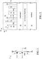
- Power supply distribution structure 108 comprises a VDD conductor 110 having a width 111, a VSSR conductor 112 having a width 113, a VBB conductor 114 having a width 115, a VDD conductor 116 having a width the same as VDD conductor 110, a VSSR conductor 118 having a width the same as VSSR conductor 112, and a VBB conductor having a width the same as the width of VBB conductor 114.
- Conductors 110, 112, 114, 116, 118, and 120 have substantially the same height and are covered by an interlayer dielectric 122.
- Power supply distribution structure 108 is a metal layer with a major purpose of providing power to the circuits of integrated circuit 100.
- the faster devices have more current flow but the amount more is reduced by the increase in voltage on the source.
- This effect of resistance 18 is significantly less on the slower devices thus the effect of resistance 18 causes a reduced differential in the current thorough faster devices and slower devices.
- the back bias voltage of VBB is unchanged because it is isolated from VSS and there is minimal loading due to being connected to only body ties.
- Shown in 5 is a further approach for forming resistance 18 using a reduced number of vias in routing conductive lines such as VSS to circuits.
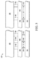
- FIG. 5 Shown in FIG. 5 is a structure 500 in which an upper conductor layer 502 provides VDD to a lower conductor layer using three vias 506, 508, and 510 spaced apart by a distance A.
- an upper conductor layer 512 that provides VSS to a lower conductor layer 504 in route to a circuit such as circuit 10. With fewer vias, the resistance between conductor layer 512 and conductor layer 514 is greater than between conductor layer 502 and conductor layer 504.
- the resistance differential represented by resistance 18 can be achieved or enhanced by reducing the number of vias.
- the integrated circuit may have a further characterization by which a second transistor including a first current electrode and a second current electrode, a third conductive line coupled between the first current electrode of the second transistor and the first supply voltage, wherein the first conductive line is further coupled to the second current electrode of the second transistor.
- the integrated circuit may have a further characterization by which the first and second conductive lines are formed in a power metal layer of the integrated circuit.
- the integrated circuit may have a further characterization by which the first and second conductive lines have a same thickness.
- the integrated circuit may further include a substrate, active electronic device structures formed on the substrate, and one or more interconnect layers coupled to the active electronic device structures, wherein the first and second conductive lines are formed over the one or more interconnect layers.
- the integrated circuit may have a further characterization by which a width of a conductive line coupled to the bulk tie is less than a width of the first conductive line and a width of the second conductive line.
- Also described is a method including forming a transistor in an active device layer of an integrated circuit, wherein the transistor includes a first current electrode, a second current electrode and a bulk tie.
- the method further includes forming interconnect structures in an interconnect layer of the integrated circuit.
- the method further includes forming a first conductive line in a power metal layer of the integrated circuit, wherein the first conductive line is coupled to the first current electrode by a first set of the interconnect structures.
Landscapes
- Engineering & Computer Science (AREA)
- Physics & Mathematics (AREA)
- Computer Hardware Design (AREA)
- Theoretical Computer Science (AREA)
- Geometry (AREA)
- General Engineering & Computer Science (AREA)
- Computer Networks & Wireless Communication (AREA)
- Evolutionary Computation (AREA)
- General Physics & Mathematics (AREA)
- Semiconductor Integrated Circuits (AREA)
- Design And Manufacture Of Integrated Circuits (AREA)
Abstract
Description
- This disclosure relates generally to integrated circuits, and more particularly, to integrated circuits with a power saving feature.
- Power savings continues to be a significant desire for integrated circuits including those that have high performance requirements such as processors and system on a chip (SoC) devices. The reduction in power usage can be desirable in a variety of applications which may or may not be a situation in which a battery is a source of power. For example, The amount of current can affect the size or character, such as conductivity, of the current carrying structure. Heat generation can be a significant issue as well. Dissipating heat can require significant extra structure such as fans and heat sinks. Also, there may be requirements relating to difficult environmental conditions at which current must be able to be dissipated. Those environmental conditions can create a situation in which undesirable current, such as leakage current, can be greatly increased from normal operations.
- Accordingly, there is a need for further improvements in controlling current in an integrated circuit.
- The present invention is illustrated by way of example and is not limited by the accompanying figures, in which like references indicate similar elements. Elements in the figures are illustrated for simplicity and clarity and have not necessarily been drawn to scale.
-
FIG. 1 is a circuit which benefits from reduced leakage current; -
FIG. 2 is a cross section of a portion of an integrated circuit that includes a power distribution grid structure that benefits the circuit ofFIG. 1 ; -
FIG. 3 is a top view of the portion of the integrated circuit ofFIG. 2 ; and -
FIG. 4 is a speed distribution of an integrated circuit that includes the features ofFIGs. 1-3 ; and -
FIG. 5 shows an alternative or addition to the structure ofFIGs. 2 and3 . - In one aspect, a resistance between a current electrode of a transistor and a power supply terminal results in a reduction in heat dissipation by reducing the off-state conduction of current through the transistor by increasing the threshold voltage with increases in current. This is better understood by reference to the drawings and the following description.
- Shown in
FIG. 1 is acircuit 10 of an integrated circuit.Circuit 10 has a P channel transistor 12, anN channel transistor 16, and aresistance 18. Transistor 12 has a first current electrode connected to a positive power supply terminal VDD, a control electrode for receiving a signal V1, a well tie connected to positive power supply terminal VDD, and a second current electrode. A well tie may also be called a bulk tie.Transistor 16 has a first current electrode connected to the second current electrode of transistor 12, a control electrode for receiving a signal V2, a second current electrode connected to a voltage node VSSR, and a substrate tie connected to a power supply terminal VBB. In typical operation, a resistance from a power supply terminal VDD, typically for receiving a positive power supply voltage, to a circuit is the same as the resistance from a power supply terminal VSS, commonly ground but typically at least negative relative to VDD. In this case, in addition to these typical resistances which are equal, there is afurther resistance 18 which is achieved to reduce power consumption in the situation where the reduction is particularly beneficial. The first current electrode of transistor 12 and the second current electrode oftransistor 16 are coupled as sources, while the second current electrode of transistor 12 and the first current electrode oftransistor 16 are coupled as drains. The control electrodes are implemented with gates oftransistors 12 and 16. - Shown in
FIG. 2 is anintegrated circuit 100 in whichcircuit 10 ofFIG. 1 is present.Integrated circuit 100 comprises asubstrate 102, an activedevice structure region 104 in a portion of and oversubstrate 102, aninterconnect region 106 over activedevice structure region 104, and a powersupply distribution structure 108 overinterconnect region 106. Powersupply distribution structure 108 comprises aVDD conductor 110 having awidth 111, aVSSR conductor 112 having awidth 113, aVBB conductor 114 having awidth 115, aVDD conductor 116 having a width the same asVDD conductor 110, aVSSR conductor 118 having a width the same asVSSR conductor 112, and a VBB conductor having a width the same as the width ofVBB conductor 114.Conductors supply distribution structure 108 is a metal layer with a major purpose of providing power to the circuits of integratedcircuit 100. Routing of power generally is achieved by similar lengths of conductive material of VDD and VSS to any given circuit. Routing of VBB is not as sensitive because very little current flows from VBB. Conductors carrying VDD and VSS, on the other hand, carry significantly more current.Width 113 is less thanwidth 111 so that more resistance is present for carrying VSS than for carrying VDD. This greater resistance is represented byresistance 18 and voltage VSSR is thus greater than voltage VSS. This is using typical terminology in which VDD is for a positive power supply voltage and VSS is for voltage that is negative with respect to the voltage at VDD. This could be reversed in a different situation so that VDD and VSS could be reversed. An effective amount of resistance differential may be as small as 5%. A greater differential such as 10% may be more effective. There may be tradeoffs that come into play that may limit the effectiveness as the differential becomes greater. But significantly higher differentials such as 30% or even more may be found to be effective. - Shown in
FIG. 3 is a top view of powersupply distribution structure 108 showingconductors circuit 100. - Shown in
FIG. 4 is adistribution 400 of many integrated circuits having the same design and construction relative to speed capability as integratedcircuit 100. The faster the speed of the integrated circuit is, the higher the leakage current is. The speed capability correlates to lower threshold voltage. Thus the integrated circuits with higher speed capability, which are designated as faster inFIG. 4 tend to consume more power than the ones designated as slower inFIG. 4 . This difference is reduced byresistance 18. - In operation, with the reduced width of the VSSR conductors,
conductors resistance 18. As current flows throughresistance 18 the voltage on the second current electrode, which is a source oftransistor 16, increases. The increase in source voltage, while the body tie remains at VSS, causes a voltage differential between the body tie and the source which has the effect of increasing the threshold voltage oftransistor 16. The increase in threshold voltage causes a decrease in current for a given voltage of input signal V2. Also the voltage increase of voltage VSSR decreases the drain to source voltage which also decreases current. For a faster device and its attendant lower threshold voltage, the current tends to be higher but that causes an even greater increase in threshold voltage and reduced drain to source voltage. Thus, the faster devices have more current flow but the amount more is reduced by the increase in voltage on the source. This effect ofresistance 18 is significantly less on the slower devices thus the effect ofresistance 18 causes a reduced differential in the current thorough faster devices and slower devices. The back bias voltage of VBB is unchanged because it is isolated from VSS and there is minimal loading due to being connected to only body ties. - Shown in 5 is a further approach for forming
resistance 18 using a reduced number of vias in routing conductive lines such as VSS to circuits. Shown inFIG. 5 is astructure 500 in which anupper conductor layer 502 provides VDD to a lower conductor layer using threevias FIG. 5 is anupper conductor layer 512 that provides VSS to alower conductor layer 504 in route to a circuit such ascircuit 10. With fewer vias, the resistance betweenconductor layer 512 andconductor layer 514 is greater than betweenconductor layer 502 andconductor layer 504. Thus the resistance differential represented byresistance 18 can be achieved or enhanced by reducing the number of vias. Afurther conductor layer 520 is aboveconductor layer 502 and connected byvias conductor layer 502. Similarly afurther conductor layer 528 is abovelayer 512 and is connected byvias layer 512.Layer 520 is significantly thicker thanconductor layer 502 and vias 522, 524, and 526 are significantly of larger diameter than that ofvias layer 528 is significantly thicker thanlayer 512 and vias 530 and 532 are of significantly larger diameter than that ofvias - Thicker conductor layers 520 and 528 are used for global power and ground distribution, respectively, whereas thinner conductor layers 502 and 512 are used for local power and ground distribution, respectively. Depending on the amount of desired resistance in the grid, the scaling of
vias - Thus it is shown that varying the conductor layers and/or the vias to tune the resistance of the grid is achievable and beneficial in increasing the threshold voltage in the proper situation to reduce leakage current, for example.
- By now it should be appreciated that there has been described an integrated circuit including a first transistor including a first current electrode, a second current electrode, and a bulk tie. The integrated circuit further includes a first conductive line coupled between the first current electrode and a first supply voltage. The integrated circuit further includes a second conductive line coupled to the second current electrode, wherein a resistance of the second conductive line is at least 5 percent greater than a resistance of the first conductive line, wherein the bulk tie is coupled to a second supply voltage, and the first supply voltage is different than the second supply voltage. The integrated circuit may have a further characterization by which the resistance of the second conductive line is at least 5 percent greater than the resistance of the first conductive line due to a width of the second conductive line being less than a width of the first conductive line. The integrated circuit may have a further characterization by which the resistance of the second conductive line is at least 5 percent greater than the resistance of the first conductive line due to a number of conductive vias coupled to the second conductive line being less a number of conductive vias coupled to the first conductive line. The integrated circuit may have a further characterization by which the first transistor is an N-channel metal oxide semiconductor, the first current electrode is a drain electrode, the second current electrode is a source electrode, and a magnitude of the first supply voltage is greater than a magnitude of the second supply voltage. The integrated circuit may have a further characterization by which the first transistor is a P-channel metal oxide semiconductor, the first current electrode is a source electrode, the second current electrode is a drain electrode, and a magnitude of the first supply voltage is greater than a magnitude of the second supply voltage. The integrated circuit may have a further characterization by which a second transistor including a first current electrode and a second current electrode, a third conductive line coupled between the first current electrode of the second transistor and the first supply voltage, wherein the first conductive line is further coupled to the second current electrode of the second transistor. The integrated circuit may have a further characterization by which the first and second conductive lines are formed in a power metal layer of the integrated circuit. The integrated circuit may have a further characterization by which the first and second conductive lines have a same thickness. The integrated circuit may further include a substrate, active electronic device structures formed on the substrate, and one or more interconnect layers coupled to the active electronic device structures, wherein the first and second conductive lines are formed over the one or more interconnect layers. The integrated circuit may have a further characterization by which a width of a conductive line coupled to the bulk tie is less than a width of the first conductive line and a width of the second conductive line.
- Also described is a method including forming a transistor in an active device layer of an integrated circuit, wherein the transistor includes a first current electrode, a second current electrode and a bulk tie. The method further includes forming interconnect structures in an interconnect layer of the integrated circuit. The method further includes forming a first conductive line in a power metal layer of the integrated circuit, wherein the first conductive line is coupled to the first current electrode by a first set of the interconnect structures. The method further includes forming a second conductive line in the power metal layer of the integrated circuit, wherein the second conductive line is coupled to the second current electrode by a second set of the interconnect structures, wherein a resistance of the second conductive line is greater than a resistance of the first conductive line to generate a bias voltage at the second current electrode that is proportional to current through the second conductive line. The method may have a further characterization by which a width of the second conductive line is at least 5 percent less than a width of the first conductive line. The method may have a further characterization by which a number of interconnect structures in the first set of the interconnect structures is greater than a number of interconnect structures in the second set of the interconnect structures. The method may further include forming a second transistor in the active device layer and forming a third conductive line in the power metal layer of the integrated circuit, wherein the third conductive line is coupled to a first current electrode of the second transistor by a third set of the interconnect structures, wherein the first conductive line is coupled to a second current electrode of the second transistor. The method may have a further characterization by which the forming interconnect structures includes forming a third set of interconnect structures coupled to the third conductive line.
- Described also is an integrated circuit including a P-channel metal oxide semiconductor transistor including a source electrode, a drain electrode and a bulk tie. The integrated circuit further includes an N-channel metal oxide semiconductor transistor including a source electrode, a drain electrode and a bulk tie. The integrated circuit further includes a first conductive line coupled to the source electrode of the PMOS transistor. The integrated circuit further includes a second conductive line coupled to the source electrode of the NMOS transistor. The integrated circuit further includes a third conductive line coupled between the drain electrode of the PMOS transistor and the drain electrode of the NMOS transistor, wherein a resistance of one of the first conductive line and the second conductive line is at least 5 percent greater than a resistance of another of the first conductive line and second conductive line. The integrated circuit may have a further characterization by which a width of the one of the first conductive line and the second conductive line is less than a width of the another one of the first conductive line and the second conductive line. The integrated circuit may further include a first set of interconnect structures coupled to the one of the first conductive line and the second conductive line and a second set of interconnect structures coupled to the another of the first conductive line and the second conductive line, wherein a number of interconnect structures in the first set is less than a number of interconnect structures in the second set. The integrated circuit may have a further characterization by which the source electrode and the bulk tie of the PMOS or NMOS transistor coupled to the one of the first conductive line and the second conductive line are coupled to a first power supply. The integrated circuit may have a further characterization by which the source electrode of the PMOS or NMOS transistor coupled to the another of the first conductive line and the second conductive line is coupled to a second power supply.
- Moreover, the terms "front," "back," "top," "bottom," "over," "under" and the like in the description and in the claims, if any, are used for descriptive purposes and not necessarily for describing permanent relative positions. It is understood that the terms so used are interchangeable under appropriate circumstances such that the embodiments of the invention described herein are, for example, capable of operation in other orientations than those illustrated or otherwise described herein.
- Although the disclosure is described herein with reference to specific embodiments, various modifications and changes can be made without departing from the scope of the present disclosure as set forth in the claims below. For example, other layers than those shown may have variations to achieve the same effect. Accordingly, the specification and figures are to be regarded in an illustrative rather than a restrictive sense, and all such modifications are intended to be included within the scope of the present disclosure. Any benefits, advantages, or solutions to problems that are described herein with regard to specific embodiments are not intended to be construed as a critical, required, or essential feature or element of any or all the claims.
- The term "coupled," as used herein, is not intended to be limited to a direct coupling or a mechanical coupling.
- Furthermore, the terms "a" or "an," as used herein, are defined as one or more than one. Also, the use of introductory phrases such as "at least one" and "one or more" in the claims should not be construed to imply that the introduction of another claim element by the indefinite articles "a" or "an" limits any particular claim containing such introduced claim element to inventions containing only one such element, even when the same claim includes the introductory phrases "one or more" or "at least one" and indefinite articles such as "a" or "an." The same holds true for the use of definite articles.
- Unless stated otherwise, terms such as "first" and "second" are used to arbitrarily distinguish between the elements such terms describe. Thus, these terms are not necessarily intended to indicate temporal or other prioritization of such elements.
Claims (15)
- An integrated circuit (10, 100), comprising:a first transistor (16 or 12) including a first current electrode, a second current electrode, and a bulk tie;a first conductive line coupled between the first current electrode and a first supply voltage (VDD for N-channel or VSS for P-channel);a second conductive line coupled to the second current electrode, wherein a resistance of the second conductive line is at least 5 percent greater than a resistance of the first conductive line;the bulk tie is coupled to a second supply voltage (VSS for N-channel or VDD for P-channel), and the first supply voltage is different than the second supply voltage.
- The integrated circuit of claim 1, wherein the resistance of the second conductive line is at least 5 percent greater than the resistance of the first conductive line due to a width of the second conductive line being less than a width of the first conductive line.
- The integrated circuit of claim 1 or claim 2, wherein the resistance of the second conductive line is at least 5 percent greater than the resistance of the first conductive line due to a number of conductive vias (516, 518) coupled to the second conductive line being less a number of conductive vias (506, 508, 510) coupled to the first conductive line.
- The integrated circuit of any one of the claims 1 to 3, wherein the first transistor is an N-channel metal oxide semiconductor (NMOS), the first current electrode is a drain electrode, the second current electrode is a source electrode, and a magnitude of the first supply voltage is greater than a magnitude of the second supply voltage.
- The integrated circuit of any one of the claims 1 to 4, wherein the first transistor is a P-channel metal oxide semiconductor (NMOS), the first current electrode is a source electrode, the second current electrode is a drain electrode, and a magnitude of the first supply voltage is greater than a magnitude of the second supply voltage.
- The integrated circuit of any one of the claims 1 to 5, further comprising:a second transistor (12) including a first current electrode and a second current electrode;a third conductive line coupled between the first current electrode of the second transistor and the first supply voltage (VDD for N-channel or VSS for P-channel);the first conductive line is further coupled to the second current electrode of the second transistor.
- The integrated circuit of any one of the claims 1 to 6, wherein the first and second conductive lines are formed in a power metal layer (108) of the integrated circuit.
- The integrated circuit of claim 7, wherein the first and second conductive lines have a same thickness.
- The integrated circuit of any one of the claims 1 to 8, further comprising:a substrate (102);active electronic device structures (104) formed on the substrate;one or more interconnect layers (106) coupled to the active device structures;the first and second conductive lines are formed over the one or more interconnect layers.
- The integrated circuit of any one of the claims 1 to 9, wherein a width of a conductive line coupled to the bulk tie is less than a width of the first conductive line and a width of the second conductive line.
- A method comprising:forming a transistor (12 or 16) in an active device layer (104) of an integrated circuit (10, 100), wherein the transistor includes a first current electrode, a second current electrode and a bulk tie;forming interconnect structures in an interconnect layer (106) of the integrated circuit;forming a first conductive line (110) in a power metal layer (108) of the integrated circuit, wherein the first conductive line is coupled to the first current electrode by a first set of the interconnect structures (506, 508, 510);forming a second conductive line (112) in the power metal layer (108) of the integrated circuit, wherein the second conductive line is coupled to the second current electrode by a second set of the interconnect structures (516), wherein a resistance of the second conductive line is greater than a resistance of the first conductive line to generate a bias voltage at the second electrode that is proportional to current through the second conductive line.
- The method of claim 11, wherein a width of the second conductive line is at least 5 percent less than a width of the first conductive line.
- The method of claim 11 or claim 12, wherein a number of interconnect structures in the first set of interconnect structures is greater than a number of interconnect structures in the second set of interconnect structures.
- The method of any one of the claims 11 to 13, further comprising:forming a second transistor (16 or 12) in the active device layer (104);forming a third conductive line (110) in the power metal layer (108) of the integrated circuit, wherein the third conductive line is coupled to a first current electrode of the second transistor by a third set of the interconnect structures,wherein the first conductive line is coupled to a second current electrode of the second transistor.
- The method of claim 14, wherein the forming interconnect structures (106) includes forming a third set of interconnect structures coupled to the third conductive line.
Applications Claiming Priority (1)
| Application Number | Priority Date | Filing Date | Title |
|---|---|---|---|
| US14/860,901 US9806019B2 (en) | 2015-09-22 | 2015-09-22 | Integrated circuit with power saving feature |
Publications (1)
| Publication Number | Publication Date |
|---|---|
| EP3147944A1 true EP3147944A1 (en) | 2017-03-29 |
Family
ID=56985489
Family Applications (1)
| Application Number | Title | Priority Date | Filing Date |
|---|---|---|---|
| EP16189794.7A Withdrawn EP3147944A1 (en) | 2015-09-22 | 2016-09-20 | Integrated circuit with power saving feature |
Country Status (3)
| Country | Link |
|---|---|
| US (1) | US9806019B2 (en) |
| EP (1) | EP3147944A1 (en) |
| CN (1) | CN106876381B (en) |
Families Citing this family (3)
| Publication number | Priority date | Publication date | Assignee | Title |
|---|---|---|---|---|
| US11733724B2 (en) * | 2021-08-20 | 2023-08-22 | Taiwan Semiconductor Manufacturing Company, Ltd. | Digital low-dropout voltage regulator |
| US12476189B2 (en) * | 2023-04-11 | 2025-11-18 | Taiwan Semiconductor Manufacturing Company Ltd. | Semiconductor device and method of manufacturing the same |
| US20250218945A1 (en) * | 2023-12-28 | 2025-07-03 | Taiwan Semiconductor Manufacturing Company, Ltd. | Device having different first metallization layer and first buried metallization layer architectures and method of manufacturing same |
Citations (5)
| Publication number | Priority date | Publication date | Assignee | Title |
|---|---|---|---|---|
| US5815029A (en) * | 1995-08-10 | 1998-09-29 | Mitsubishi Denki Kabsuhiki Kaisha | Semiconductor circuit and semiconductor circuit device |
| US20070180419A1 (en) * | 2003-06-02 | 2007-08-02 | Sherlekar Deepak D | Various methods and apparatuses to route multiple power rails to a cell |
| US20070210405A1 (en) * | 2006-03-08 | 2007-09-13 | Masanori Tsutsumi | Semiconductor integrated circuit device and power source wiring method therefor |
| US20090045480A1 (en) * | 2006-03-02 | 2009-02-19 | Hiroki Matsunaga | Semiconductor integrated circuit |
| US20120249182A1 (en) * | 2011-03-30 | 2012-10-04 | Synopsys, Inc. | Power Routing in Standard Cell Designs |
Family Cites Families (12)
| Publication number | Priority date | Publication date | Assignee | Title |
|---|---|---|---|---|
| US4948747A (en) * | 1989-12-18 | 1990-08-14 | Motorola, Inc. | Method of making an integrated circuit resistor |
| KR100243295B1 (en) | 1997-06-26 | 2000-02-01 | 윤종용 | Back bias generator and method for generating the semiconductor device |
| JPH11183507A (en) * | 1997-12-25 | 1999-07-09 | Fujikura Ltd | Semiconductor sensor |
| JP2001308282A (en) * | 2000-04-19 | 2001-11-02 | Nec Corp | Semiconductor device |
| JP4463946B2 (en) | 2000-07-03 | 2010-05-19 | Necエレクトロニクス株式会社 | Low power consumption circuit |
| US6744659B1 (en) | 2002-12-09 | 2004-06-01 | Analog Devices, Inc. | Source-biased memory cell array |
| US7115460B2 (en) | 2003-09-04 | 2006-10-03 | Taiwan Semiconductor Manufacturing Company, Ltd. | Standard cell back bias architecture |
| KR100558046B1 (en) * | 2004-12-28 | 2006-03-07 | 주식회사 하이닉스반도체 | Most transistor with temperature insensitive saturation current and constant voltage generator using the same |
| JP2007122814A (en) | 2005-10-28 | 2007-05-17 | Oki Electric Ind Co Ltd | Semiconductor integrated circuit and leakage current reducing method |
| JP5186925B2 (en) * | 2008-01-11 | 2013-04-24 | 株式会社リコー | Semiconductor device and manufacturing method thereof |
| JPWO2015083289A1 (en) * | 2013-12-06 | 2017-03-16 | ルネサスエレクトロニクス株式会社 | Semiconductor device |
| US9276140B1 (en) * | 2014-09-16 | 2016-03-01 | Amazon Technologies, Inc. | Imager module with interposer chip |
-
2015
- 2015-09-22 US US14/860,901 patent/US9806019B2/en active Active
-
2016
- 2016-09-08 CN CN201610811518.2A patent/CN106876381B/en active Active
- 2016-09-20 EP EP16189794.7A patent/EP3147944A1/en not_active Withdrawn
Patent Citations (5)
| Publication number | Priority date | Publication date | Assignee | Title |
|---|---|---|---|---|
| US5815029A (en) * | 1995-08-10 | 1998-09-29 | Mitsubishi Denki Kabsuhiki Kaisha | Semiconductor circuit and semiconductor circuit device |
| US20070180419A1 (en) * | 2003-06-02 | 2007-08-02 | Sherlekar Deepak D | Various methods and apparatuses to route multiple power rails to a cell |
| US20090045480A1 (en) * | 2006-03-02 | 2009-02-19 | Hiroki Matsunaga | Semiconductor integrated circuit |
| US20070210405A1 (en) * | 2006-03-08 | 2007-09-13 | Masanori Tsutsumi | Semiconductor integrated circuit device and power source wiring method therefor |
| US20120249182A1 (en) * | 2011-03-30 | 2012-10-04 | Synopsys, Inc. | Power Routing in Standard Cell Designs |
Also Published As
| Publication number | Publication date |
|---|---|
| US20170084535A1 (en) | 2017-03-23 |
| CN106876381B (en) | 2022-02-25 |
| US9806019B2 (en) | 2017-10-31 |
| CN106876381A (en) | 2017-06-20 |
Similar Documents
| Publication | Publication Date | Title |
|---|---|---|
| CN114762113B (en) | Semiconductor devices | |
| JPH11195975A (en) | Level conversion circuit and semiconductor integrated circuit device | |
| EP2341537A2 (en) | Flexible CMOS library architecture for leakage power and variability reduction | |
| CN101154659B (en) | Semiconductor integrated circuit | |
| US10453840B2 (en) | Semiconductor integrated circuit | |
| US10211205B2 (en) | Field effect transistor structure for reducing contact resistance | |
| TWI739811B (en) | Layout of semiconductor device, semiconductor device and operation thereof | |
| CN104517963B (en) | State keeps power supply gating unit | |
| US9806019B2 (en) | Integrated circuit with power saving feature | |
| US12316312B2 (en) | Power gating for multiple backside voltage planes | |
| US7542329B2 (en) | Virtual power rails for integrated circuits | |
| WO2017157117A1 (en) | Electrostatic discharge (esd) protective circuit for integrated circuit | |
| CN101667047A (en) | Voltage regulation module, printed circuit board and substrate biasing method | |
| JP2014140031A (en) | Method and apparatus for power-down of analog integrated circuit | |
| US6624663B2 (en) | Low threshold voltage silicon-on-insulator clock gates | |
| CN101490849A (en) | Transistors and Semiconductor Devices | |
| Kuroda et al. | Variable threshold-voltage CMOS technology | |
| CN1909232B (en) | Semiconductor integrated circuit | |
| Dadoria et al. | Leakage reduction by using FinFET technique for nanoscale technology circuits | |
| Kumar | Effects of scaling on MOS device performance | |
| JP4397066B2 (en) | Latch circuit | |
| CN106783839A (en) | Electronic equipment specifically for preventing overvoltage | |
| KR100835425B1 (en) | MTCSMOS Semiconductor Integrated Circuits | |
| US6917082B1 (en) | Gate-body cross-link circuitry for metal-oxide-semiconductor transistor circuits | |
| US6269042B1 (en) | I/O circuit of semiconductor integrated device |
Legal Events
| Date | Code | Title | Description |
|---|---|---|---|
| PUAI | Public reference made under article 153(3) epc to a published international application that has entered the european phase |
Free format text: ORIGINAL CODE: 0009012 |
|
| STAA | Information on the status of an ep patent application or granted ep patent |
Free format text: STATUS: THE APPLICATION HAS BEEN PUBLISHED |
|
| AK | Designated contracting states |
Kind code of ref document: A1 Designated state(s): AL AT BE BG CH CY CZ DE DK EE ES FI FR GB GR HR HU IE IS IT LI LT LU LV MC MK MT NL NO PL PT RO RS SE SI SK SM TR |
|
| AX | Request for extension of the european patent |
Extension state: BA ME |
|
| STAA | Information on the status of an ep patent application or granted ep patent |
Free format text: STATUS: REQUEST FOR EXAMINATION WAS MADE |
|
| RIN1 | Information on inventor provided before grant (corrected) |
Inventor name: WARNER, JEFF Inventor name: TIPPLE, DAVID Inventor name: JARRAR, ANIS M |
|
| 17P | Request for examination filed |
Effective date: 20170929 |
|
| RBV | Designated contracting states (corrected) |
Designated state(s): AL AT BE BG CH CY CZ DE DK EE ES FI FR GB GR HR HU IE IS IT LI LT LU LV MC MK MT NL NO PL PT RO RS SE SI SK SM TR |
|
| STAA | Information on the status of an ep patent application or granted ep patent |
Free format text: STATUS: EXAMINATION IS IN PROGRESS |
|
| 17Q | First examination report despatched |
Effective date: 20200210 |
|
| STAA | Information on the status of an ep patent application or granted ep patent |
Free format text: STATUS: THE APPLICATION IS DEEMED TO BE WITHDRAWN |
|
| 18D | Application deemed to be withdrawn |
Effective date: 20200623 |