EP3147943A1 - Multi-level signaling for on-package chip-to-chip interconnect through silicon bridge - Google Patents
Multi-level signaling for on-package chip-to-chip interconnect through silicon bridge Download PDFInfo
- Publication number
- EP3147943A1 EP3147943A1 EP16188764.1A EP16188764A EP3147943A1 EP 3147943 A1 EP3147943 A1 EP 3147943A1 EP 16188764 A EP16188764 A EP 16188764A EP 3147943 A1 EP3147943 A1 EP 3147943A1
- Authority
- EP
- European Patent Office
- Prior art keywords
- semiconductor die
- analog
- binary signals
- signal
- digital
- Prior art date
- Legal status (The legal status is an assumption and is not a legal conclusion. Google has not performed a legal analysis and makes no representation as to the accuracy of the status listed.)
- Granted
Links
Images




Classifications
-
- G—PHYSICS
- G06—COMPUTING OR CALCULATING; COUNTING
- G06F—ELECTRIC DIGITAL DATA PROCESSING
- G06F13/00—Interconnection of, or transfer of information or other signals between, memories, input/output devices or central processing units
- G06F13/14—Handling requests for interconnection or transfer
- G06F13/20—Handling requests for interconnection or transfer for access to input/output bus
-
- H—ELECTRICITY
- H10—SEMICONDUCTOR DEVICES; ELECTRIC SOLID-STATE DEVICES NOT OTHERWISE PROVIDED FOR
- H10W—GENERIC PACKAGES, INTERCONNECTIONS, CONNECTORS OR OTHER CONSTRUCTIONAL DETAILS OF DEVICES COVERED BY CLASS H10
- H10W70/00—Package substrates; Interposers; Redistribution layers [RDL]
- H10W70/60—Insulating or insulated package substrates; Interposers; Redistribution layers
- H10W70/62—Insulating or insulated package substrates; Interposers; Redistribution layers characterised by their interconnections
- H10W70/65—Shapes or dispositions of interconnections
-
- G—PHYSICS
- G06—COMPUTING OR CALCULATING; COUNTING
- G06F—ELECTRIC DIGITAL DATA PROCESSING
- G06F13/00—Interconnection of, or transfer of information or other signals between, memories, input/output devices or central processing units
- G06F13/38—Information transfer, e.g. on bus
- G06F13/42—Bus transfer protocol, e.g. handshake; Synchronisation
- G06F13/4204—Bus transfer protocol, e.g. handshake; Synchronisation on a parallel bus
- G06F13/4221—Bus transfer protocol, e.g. handshake; Synchronisation on a parallel bus being an input/output bus, e.g. ISA bus, EISA bus, PCI bus, SCSI bus
-
- H—ELECTRICITY
- H10—SEMICONDUCTOR DEVICES; ELECTRIC SOLID-STATE DEVICES NOT OTHERWISE PROVIDED FOR
- H10W—GENERIC PACKAGES, INTERCONNECTIONS, CONNECTORS OR OTHER CONSTRUCTIONAL DETAILS OF DEVICES COVERED BY CLASS H10
- H10W70/00—Package substrates; Interposers; Redistribution layers [RDL]
- H10W70/60—Insulating or insulated package substrates; Interposers; Redistribution layers
-
- H—ELECTRICITY
- H10—SEMICONDUCTOR DEVICES; ELECTRIC SOLID-STATE DEVICES NOT OTHERWISE PROVIDED FOR
- H10W—GENERIC PACKAGES, INTERCONNECTIONS, CONNECTORS OR OTHER CONSTRUCTIONAL DETAILS OF DEVICES COVERED BY CLASS H10
- H10W70/00—Package substrates; Interposers; Redistribution layers [RDL]
- H10W70/60—Insulating or insulated package substrates; Interposers; Redistribution layers
- H10W70/611—Insulating or insulated package substrates; Interposers; Redistribution layers for connecting multiple chips together
-
- H—ELECTRICITY
- H10—SEMICONDUCTOR DEVICES; ELECTRIC SOLID-STATE DEVICES NOT OTHERWISE PROVIDED FOR
- H10W—GENERIC PACKAGES, INTERCONNECTIONS, CONNECTORS OR OTHER CONSTRUCTIONAL DETAILS OF DEVICES COVERED BY CLASS H10
- H10W70/00—Package substrates; Interposers; Redistribution layers [RDL]
- H10W70/60—Insulating or insulated package substrates; Interposers; Redistribution layers
- H10W70/611—Insulating or insulated package substrates; Interposers; Redistribution layers for connecting multiple chips together
- H10W70/616—Insulating or insulated package substrates; Interposers; Redistribution layers for connecting multiple chips together package substrates, interposers or redistribution layers combined with bridge chips
- H10W70/618—Insulating or insulated package substrates; Interposers; Redistribution layers for connecting multiple chips together package substrates, interposers or redistribution layers combined with bridge chips the bridge chips being embedded in the package substrates, interposers or redistribution layers
-
- H—ELECTRICITY
- H10—SEMICONDUCTOR DEVICES; ELECTRIC SOLID-STATE DEVICES NOT OTHERWISE PROVIDED FOR
- H10W—GENERIC PACKAGES, INTERCONNECTIONS, CONNECTORS OR OTHER CONSTRUCTIONAL DETAILS OF DEVICES COVERED BY CLASS H10
- H10W90/00—Package configurations
-
- H—ELECTRICITY
- H10—SEMICONDUCTOR DEVICES; ELECTRIC SOLID-STATE DEVICES NOT OTHERWISE PROVIDED FOR
- H10W—GENERIC PACKAGES, INTERCONNECTIONS, CONNECTORS OR OTHER CONSTRUCTIONAL DETAILS OF DEVICES COVERED BY CLASS H10
- H10W90/00—Package configurations
- H10W90/401—Package configurations characterised by multiple insulating or insulated package substrates, interposers or RDLs
-
- G—PHYSICS
- G06—COMPUTING OR CALCULATING; COUNTING
- G06F—ELECTRIC DIGITAL DATA PROCESSING
- G06F2213/00—Indexing scheme relating to interconnection of, or transfer of information or other signals between, memories, input/output devices or central processing units
- G06F2213/0016—Inter-integrated circuit (I2C)
-
- H—ELECTRICITY
- H10—SEMICONDUCTOR DEVICES; ELECTRIC SOLID-STATE DEVICES NOT OTHERWISE PROVIDED FOR
- H10W—GENERIC PACKAGES, INTERCONNECTIONS, CONNECTORS OR OTHER CONSTRUCTIONAL DETAILS OF DEVICES COVERED BY CLASS H10
- H10W90/00—Package configurations
- H10W90/701—Package configurations characterised by the relative positions of pads or connectors relative to package parts
- H10W90/721—Package configurations characterised by the relative positions of pads or connectors relative to package parts of bump connectors
- H10W90/724—Package configurations characterised by the relative positions of pads or connectors relative to package parts of bump connectors between a chip and a stacked insulating package substrate, interposer or RDL
Definitions
- the present invention relates generally to data communications. More particularly, the present invention relates to circuitry for data communications between integrated circuit devices.
- High-speed data links are used to communicate data between integrated circuit devices in a system.
- Serial interface protocols have been developed at increasingly fast data-rates for such high-speed links.
- an apparatus for data communication between at least two in-package semiconductor dies is disclosed.
- a digital-to-analog converter (DAC) converts a set of binary signals to an analog signal level (out of 2 n possibilities, for example).
- a silicon bridge transmits the analog signal to a second semiconductor die in the package.
- a method of data communication between at least two in-package semiconductor dies is disclosed.
- a plurality of binary signals is converted to an analog signal by a digital-to-analog converter on a first semiconductor die.
- the analog signal is transmitted through a silicon bridge to a second semiconductor die.
- a system for transmitting a multiple-level data signal across an interposer from a first integrated circuit to a second integrated circuit is also disclosed.
- a first register on the first semiconductor die receives a multiple-bit data signal from logic circuitry on the first integrated circuit and outputs a plurality of binary signals.
- a digital-to-analog converter on the first integrated circuit each receives the plurality of binary signals, converts the plurality of binary signals to an analog signal, and drives the analog signal to an output node on the first integrated circuit.
- a connection is provided through the interposer between the output node of the first integrated circuit and an input node of the second integrated circuit.
- a first digital-to-analog converter on a first semiconductor die in a package converts a first plurality of binary signals to a first analog signal and drives the first analog signal to a silicon bridge.
- a first analog-to-digital converter on the first semiconductor die that receives a second analog signal from the silicon bridge and converts the second analog signal to a first plurality of recovered binary signals.
- a plurality of binary signals are received from first logic circuitry in a first semiconductor die in a package.
- the plurality of binary signals are converted to a first analog signal using an digital-to-analog converter on the first semiconductor die.
- the first analog signal is driven from the first semiconductor die to a silicon bridge.
- One embodiment of the invention relates to a packaged device containing multiple semiconductor die (integrated circuit chips) connected by an embedded silicon bridge (an interposer).
- an interposer For such a package device, increasing the interconnect bandwidth between the die (assuming binary signaling) either costs more micro-bumps of interconnect, or entails increasing the design complexity in the clocking network to support a higher data-rate (for example, to greater than one gigabits per second).
- the present solution uses a data signal with multiple (three or more) logical levels on one lane to transfer more than one bit of data per symbol on the lane.
- a lane may correspond to a micro-bump for a single-ended signal or a pair of micro-bumps for a differential signal.
- sending more than one bit per symbol for each lane enables using fewer micro-bumps for the same baud-rate.
- sending more than one bit per symbol for each lane enables running at a lower baud-rate for the same number of micro-bumps.
- One specific implementation uses a 4-level transmit digital-to-analog converter (DAC) to send, and a 4-level receive analog-to-digital converter (ADC) to receive, two bits per symbol for each lane.
- DAC digital-to-analog converter
- ADC analog-to-digital converter
- Another specific implementation uses an 8-level transmit DAC to send, and an 8-level receive ADC to receive, three bits per symbol for each lane.
- Another specific implementation uses a 16-level transmit DAC to send, and an 16-level receive ADC to receive, four bits per symbol for each lane.
- a lower baud-rate simplifies clocking and mitigates concerns over on-chip pin-to-pin skew, power supply noise, and duty cycle variations.
- the lower baud-rate allows using simpler circuits to decode the data.
- this solution not only reduces symbol interference, but it may also lead to reduction of the overall area and/or number of micro-bumps (interconnections) needed for a given data-rate.
- FIG. 1 is a schematic diagram illustrating two semiconductor dies (106-1 and 106-2) interconnected through a silicon bridge 108 in accordance with an embodiment of the invention. As shown, the two semiconductor dies (integrated circuit chips) may be interconnected with micro-bump interconnections 107 to circuitry on a laminate substrate 102.
- the laminate substrate 102 may include an embedded silicon bridge 108 that acts as an interposer between the two semiconductor dies (106-1 and 106-2).
- the micro-bumps 107 may be used to interconnect circuitry on each of the semiconductor dies with circuitry on the silicon bridge 108.
- the two semiconductor dies (106-1 and 106-2) may communicate by way of a multiple-lane data channel that goes through the silicon bridge 108.
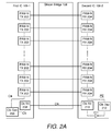
- FIG. 2A is a block diagram depicting multiple PAM-N transmitter circuits 202 of a first semiconductor die 106-1 connecting via a silicon bridge 108 to multiple PAM-N receiver circuits 204 of a second semiconductor die 106-2 in accordance with an embodiment of the invention.
- N is three or greater such that more than one bit is transmitted per symbol.
- N is 4, 8, 16, etc.
- N 2 n , where n is an integer that is two or more.
- a clock generation circuit 206 on the first semiconductor die 106-1 may generate the clock signal Clk, which may be distributed to each of the PAM-N transmitter circuits 202 and to a clock transmitter circuit 208.
- the clock signal Clk may be a CMOS clock signal, for example.
- the PAM-N transmitter circuits 202 may use the clock signal Clk to determine the baud-rate and timing for data transmission via the multiple lanes.
- the clock transmitter (Clk TX) circuit 208 on the first semiconductor die 106-1 may be used to transmit the clock signal Clk via the silicon bridge 108 to the second semiconductor die 106-2.
- the clock signal Clk may be received by the clock receiver (Clk RX) circuit on the second semiconductor die 106-2.
- An inverter circuit 211 may be used to generate the inverted clock signal Clk
- clock distribution circuitry 212 may distribute the inverted clock signal Clk to the PAM-N receiver circuits 204 on the second semiconductor die 106-2.
- the PAM-N receiver circuits 204 may use the inverted clock signal Clk to determine the timing for data reception on the multiple lanes.
- the clock edges that are 180 degrees apart may be used to time symbol transitions by a transmitter circuit 202 and to sample the data signal by a corresponding receiver circuit 204. For example, if the rising edge of the clock signal Clk may be used to time the transitions between symbols by the PAM-N transmitter circuit 202, then the rising edge of the inverted clock signal Clk may be used for sampling data by a PAM-N receiver circuit 204.
- FIG. 2B is a block diagram depicting multiple PAM-N transmitter circuits 202 of a first semiconductor die 106-1 connecting via a silicon bridge 108 to multiple PAM-N receiver circuits 104 of a second semiconductor die 106-2 and multiple PAM-N transmitter circuits 202 of the second semiconductor die 106-2 connecting via the silicon bridge 108 to multiple PAM-N receiver circuits 104 of the first semiconductor die 106-1 in accordance with an embodiment of the invention.
- the circuits in FIG. 2B operate as described above in relation to FIG. 2A . However, while FIG. 2A provides one-way communication from the first semiconductor die 106-1 to the second semiconductor die 106-2, FIG. 2B provides bi-directional communication between the first and second semiconductor dies.
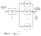
- FIG. 3 is a block diagram of a PAM-N transmitter circuit 202 on the first semiconductor die 106-1 in accordance with an embodiment of the invention.
- the PAM-N transmitter circuit 202 may include an n-bit register circuit 302 and a N-level digital-to-analog converter (DAC) circuit 304.
- DAC digital-to-analog converter
- N 2 n , where n is an integer that is two or more.
- the n-bit register circuit 302 may receive and latch n bits of data.
- the data may be received in parallel from logic circuitry on the first semiconductor die 106-1.
- the timing for the n-bit register circuit 302 may be provided by a clock edge (for example, the rising edge) of the clock signal Clk, described above in relation to FIG. 2A .
- the n binary signals output from the n-bit register circuit 302 may be provided to the N-level DAC circuit 304.
- the N-level DAC circuit 304 may convert the n binary signals to an analog signal.
- the analog signal may be 0 volts; if the 4 binary signals are logical 0001, then the analog signal may be 0.1 volts; if the 4 binary signals are logical 0010, then the analog signal may be 0.2 volts; if the 4 binary signals are logical 0011, then the analog signal may be 0.3 volts; ...; if the 4 binary signals are logical 1111, then the analog signal may be 1.5 volts.
- the analog signal goes from the output node 306 through the silicon bridge 108 to a corresponding PAM-N receiver circuit 204 on the second semiconductor die 106-2.
- PAM-16 may be implemented such that one lane carries four bits.
- Specific multiple-lane implementations to achieve an aggregate data rate of 32 Gbps may be as follows: 16 lanes of PAM-16 with a 500 MHz clock; or 8 lanes of PAM-16 with a 1 GHz clock; or 4 lanes of PAM-16 with a 2 GHz clock.
- power may be scaled with the data rate.
- the driver circuits may be made slower with lower power for lower data rates.
- FIG. 4 is a block diagram of a PAM-N receiver circuit 204 on the second semiconductor die 106-2 in accordance with an embodiment of the invention.
- the PAM-N receiver circuit 204 may include an N-level analog-to-digital converter (ADC) circuit 402, and an n-bit register circuit 404.
- ADC analog-to-digital converter
- N 2 n , where n is an integer that is two or more.
- the analog data signal may be received by the N-level ADC circuit 402.
- the N-level ADC circuit 402 may be implemented with N-1 comparators, and the structure of the N-level ADC circuit 402 may be flashed or pipelined.
- the N-level ADC circuit 402 converts the analog signal to n recovered binary signals.
- the n recovered binary signals may be provided in parallel to, and sampled by, the n-bit register circuit 404 to recover an n-bit data signal.
- the timing for the sampling may be provided by a clock edge (for example, the rising edge) from the inverted clock signal Clk , described above in relation to FIG. 2A .
- the n-bit register circuit 404 may output the recovered n-bit data signal in parallel to logic circuitry on the second semiconductor die 106-2 for further processing and use.
- FIG. 5 is a flow chart of a method 500 of transmitting a multi-level amplitude signal to a silicon bridge in accordance with an embodiment of the invention.
- the method may be performed by using a PAM-N transmitter 202 of the first semiconductor die 106-1.
- the n binary signals may be converted to an analog signal. As described above in relation to FIG. 3 , the conversion may be performed by a DAC circuit. Per step 508, the output of the DAC circuit may be combined and switched simultaneously to drive the analog signal from the first die 106-1 through the silicon bridge to the second die 106-2.
- FIG. 6 is a flow chart of a method 600 of receiving a multi-level amplitude signal from a silicon bridge in accordance with an embodiment of the invention.
- the method 600 may be performed by using a PAM-N receiver 204 of the second semiconductor die 106-2.
- each comparator may be calibrated for offset correction.
- the analog data signal may be received by an N-level ADC circuit 402.
- the N-level ADC circuit 402 may be implemented with N-1 comparators, and the structure of the N-level ADC circuit 402 may be flashed or pipelined.
- the analog signal may be converted to n recovered binary signals.
- the n recovered binary signals may be provided in parallel to, and sampled by, the n-bit register circuit 404 to recover an n-bit data signal.
- the timing for the sampling may be provided by a clock edge (for example, the rising edge) from the inverted clock signal Clk , described above in relation to FIG. 2 .
- the recovered n-bit data signal may be output from the n-bit register circuit 404 in parallel to logic circuitry on the second semiconductor die 106-2 for further processing and use.
- FIG. 7 is a simplified partial block diagram of a field programmable gate array (FPGA) 10 that may be arranged or configured to include one or more of the circuits disclosed herein in accordance with an embodiment of the invention.
- FPGA field programmable gate array
- PLDs programmable logic devices
- CPLDs complex programmable logic devices
- PLAs programmable logic arrays
- DSPs digital signal processors
- ASICs application specific integrated circuits
- FPGA 10 includes within its "core" a two-dimensional array of programmable logic array blocks (or LABs) 12 that are interconnected by a network of column and row interconnect conductors of varying length and speed.
- LABs 12 include multiple (e.g., ten) logic elements (or LEs).
- An LE is a programmable logic block that provides for efficient implementation of user defined logic functions.
- An FPGA has numerous logic elements that can be configured to implement various combinatorial and sequential functions. The logic elements have access to a programmable interconnect structure. The programmable interconnect structure can be programmed to interconnect the logic elements in almost any desired configuration.
- FPGA 10 may also include a distributed memory structure including random access memory (RAM) blocks of varying sizes provided throughout the array.
- RAM random access memory
- the RAM blocks include, for example, blocks 14, blocks 16, and block 18. These memory blocks can also include shift registers and FIFO buffers.
- FPGA 10 may further include digital signal processing (DSP) blocks 20 that can implement, for example, multipliers with add or subtract features.
- DSP digital signal processing
- IOEs 22 located, in this example, around the periphery of the chip support numerous single-ended and differential input/output standards. Each IOE 22 is coupled to an external terminal (i.e., a pin) of FPGA 10.
- a transceiver (TX/RX) channel array may be arranged as shown, for example, with each TX/RX channel circuit 30 being coupled to several LABs.
- a TX/RX channel circuit 30 may include, among other circuitry, the transmitter and receiver circuitry described herein.
- FPGA 10 is described herein for illustrative purposes only and that the present invention can be implemented in many different types of PLDs, FPGAs, and ASICs.
- FIG. 8 is a block diagram of an exemplary digital system 50 that may employ multi-level amplitude signaling in accordance with an embodiment of the invention. As shown, system 50 may include an FPGA as one of several components.
- System 50 may be, for example, a programmed digital computer system, digital signal processing system, specialized digital switching network, or other processing system.
- System 50 may be designed for a wide variety of applications such as telecommunications systems, automotive systems, control systems, consumer electronics, personal computers, Internet communications and networking, and others. Further, system 50 may be provided on a single board, on multiple boards, or within multiple enclosures.
- system 50 includes a processing unit 52, a memory unit 54, and an input/output (I/O) unit 56 interconnected together by one or more buses.
- FPGA 58 is embedded in processing unit 52.
- FPGA 58 may serve many different purposes within the system 50.
- FPGA 58 may, for example, be a logical building block of processing unit 52, supporting its internal and external operations.
- FPGA 58 is programmed to implement the logical functions necessary to carry on its particular role in system operation.
- FPGA 58 can be specially coupled to memory 54 through connection 60 and to I/O unit 56 through connection 62.
- Processing unit 52 may direct data to an appropriate system component for processing or storage, execute a program stored in memory 54, receive and transmit data via I/O unit 56, or other similar function.
- Processing unit 52 may be a central processing unit (CPU), microprocessor, floating point coprocessor, graphics coprocessor, hardware controller, microcontroller, field programmable gate array programmed for use as a controller, network controller, or any type of processor or controller. Furthermore, in many embodiments, there is often no need for a CPU.
- FPGA 58 may control the logical operations of the system.
- FPGA 58 acts as a reconfigurable processor that may be reprogrammed as needed to handle a particular computing task.
- FPGA 58 may itself include an embedded microprocessor.
- Memory unit 54 may be a random access memory (RAM), read only memory (ROM), fixed or flexible disk media, flash memory, tape, or any other storage means, or any combination of these storage means.
- Embodiment 1 An apparatus for data communication between at least two in-package semiconductor dies, the apparatus comprising:
- Embodiment 3 The apparatus of Embodiment 1 or 2, further comprising:
- Embodiment 4 The apparatus of Embodiment 1 or 2, further comprising:
- Embodiment 5 The apparatus of Embodiment 4, further comprising:
- Embodiment 6 The apparatus of Embodiment 5, further comprising:
- Embodiment 7 The apparatus of Embodiment 6, wherein the clock signal is provided to the first register and provides timing for switching the binary signals.
- Embodiment 8 The apparatus of Embodiment 7, further comprising:
- Embodiment 9 A method of data communication between at least two in-package semiconductor dies, the method comprising:
- Embodiment 11 The method of Embodiment 9 or 10, further comprising: receiving by a first register a multiple-bit data signal from logic circuitry on the first semiconductor die; and outputting the plurality of binary signals to the digital-to-analog converter.
- Embodiment 12 The method of Embodiment 9 or 10, further comprising: converting the analog signal to a plurality of recovered binary signals by an analog-to-digital converter on the second semiconductor die.
- Embodiment 13 The method of Embodiment 12, further comprising: receiving by a first register a multiple-bit data signal from logic circuitry on the first semiconductor die; outputting the plurality of binary signals to the digital-to-analog converter; receiving by a second register the plurality of recovered binary signals from the analog-to-digital converter; and outputting an multiple-bit recovered data signal to logic circuitry on the second semiconductor die.
- Embodiment 14 The method of any one of Embodiments 9-13, further comprising:
- Embodiment 15 The method of Embodiment 14, wherein the clock signal is provided to the first register and provides timing for switching the binary signals.
- Embodiment 16 The method of Embodiment 15, further comprising: receiving the clock signal and outputting an inverted clock signal by an inverter on the second semiconductor die; and using the inverted clock signal by the second register to provide timing for sampling of the analog signal.
- Embodiment 17 An apparatus for data communication between at least two in-package semiconductor dies, the apparatus comprising:
- Embodiment 18 The apparatus of Embodiment 17, further comprising:
Landscapes
- Engineering & Computer Science (AREA)
- Theoretical Computer Science (AREA)
- Physics & Mathematics (AREA)
- General Engineering & Computer Science (AREA)
- General Physics & Mathematics (AREA)
- Semiconductor Integrated Circuits (AREA)
Abstract
Description
- The present invention relates generally to data communications. More particularly, the present invention relates to circuitry for data communications between integrated circuit devices.
- High-speed data links are used to communicate data between integrated circuit devices in a system. Serial interface protocols have been developed at increasingly fast data-rates for such high-speed links.
- The invention is defined in claims 1 and 9, respectively. Particular embodiments are set out in the dependent claims.
- In particular, an apparatus for data communication between at least two in-package semiconductor dies is disclosed. On the first semiconductor die in a package, a digital-to-analog converter (DAC) converts a set of binary signals to an analog signal level (out of 2n possibilities, for example). A silicon bridge transmits the analog signal to a second semiconductor die in the package.
- Further, a method of data communication between at least two in-package semiconductor dies is disclosed. A plurality of binary signals is converted to an analog signal by a digital-to-analog converter on a first semiconductor die. The analog signal is transmitted through a silicon bridge to a second semiconductor die.
- A system for transmitting a multiple-level data signal across an interposer from a first integrated circuit to a second integrated circuit is also disclosed. A first register on the first semiconductor die receives a multiple-bit data signal from logic circuitry on the first integrated circuit and outputs a plurality of binary signals. A digital-to-analog converter on the first integrated circuit each receives the plurality of binary signals, converts the plurality of binary signals to an analog signal, and drives the analog signal to an output node on the first integrated circuit. A connection is provided through the interposer between the output node of the first integrated circuit and an input node of the second integrated circuit.
- Moreover, another apparatus for data communication between at least two in-package semiconductor dies is also disclosed. A first digital-to-analog converter on a first semiconductor die in a package converts a first plurality of binary signals to a first analog signal and drives the first analog signal to a silicon bridge. A first analog-to-digital converter on the first semiconductor die that receives a second analog signal from the silicon bridge and converts the second analog signal to a first plurality of recovered binary signals.
- Further, another method for data communication between at least two in-package semiconductor dies is disclosed. A plurality of binary signals are received from first logic circuitry in a first semiconductor die in a package. The plurality of binary signals are converted to a first analog signal using an digital-to-analog converter on the first semiconductor die. The first analog signal is driven from the first semiconductor die to a silicon bridge.
- Other embodiments, aspects, and features are also disclosed.
-
-
FIG. 1 is a schematic diagram illustrating two semiconductor dies interconnected through a silicon bridge in accordance with an embodiment of the invention. -
FIG. 2A is a block diagram depicting multiple PAM-N transmitter circuits of a first semiconductor die connecting via a silicon bridge to multiple PAM-N receiver circuits of a second semiconductor die in accordance with an embodiment of the invention. -
FIG. 2B is a block diagram depicting multiple PAM-N transmitter circuits of a first semiconductor die connecting via a silicon bridge to multiple PAM-N receiver circuits of a second semiconductor die and multiple PAM-N transmitter circuits of the second semiconductor die connecting via the silicon bridge to multiple PAM-N receiver circuits of the first semiconductor die in accordance with an embodiment of the invention. -
FIG. 3 is a block diagram of a PAM-N transmitter circuit in accordance with an embodiment of the invention. -
FIG. 4 is a block diagram of a PAM-N receiver circuit in accordance with an embodiment of the invention. -
FIG. 5 is a flow chart of a method of transmitting a multi-level amplitude signal to a silicon bridge in accordance with an embodiment of the invention. -
FIG. 6 is a flow chart of a method of receiving a multi-level amplitude signal from a silicon bridge in accordance with an embodiment of the invention. -
FIG. 7 is a simplified partial block diagram of a field programmable gate array that may be arranged or configured to include one or more of the circuits disclosed herein in accordance with an embodiment of the invention. -
FIG. 8 is a block diagram of an exemplary digital system that may employ a multi-level signaling data link in accordance with an embodiment of the invention. - The conventional wisdom is to use PAM-N signaling to lower the signaling baud rate for serial links when signal loss at higher baud rate is too high. In the case of interconnections through a silicon bridge (or other similar interposer), channel loss is generally very low. Hence, the conventional wisdom would be against using PAM-N signaling across a silicon bridge.
- The presently-disclosed solution goes counter to this conventional wisdom and implements PAM-N signaling across a silicon bridge. This solution is based on the determination by the applicant that, despite no need to improve channel loss across a silicon bridge (or similar interposer), using PAM-N signaling simplifies and improves other different issues, specifically for a parallel interface. These issues include clock generation and distribution, cross talk, simultaneous switching noise, and pin-to-pin skew.
- One embodiment of the invention relates to a packaged device containing multiple semiconductor die (integrated circuit chips) connected by an embedded silicon bridge (an interposer). For such a package device, increasing the interconnect bandwidth between the die (assuming binary signaling) either costs more micro-bumps of interconnect, or entails increasing the design complexity in the clocking network to support a higher data-rate (for example, to greater than one gigabits per second).
- However, issues such as on-die variations, pin-to-pin skew, duty cycle variations, high-speed clock generation and distribution and so on, cost additional area and power to accommodate. These costs offset the noise benefits of simple binary signaling.
- The present solution uses a data signal with multiple (three or more) logical levels on one lane to transfer more than one bit of data per symbol on the lane. A lane may correspond to a micro-bump for a single-ended signal or a pair of micro-bumps for a differential signal. Hence, in this solution, for a given aggregate data-rate, sending more than one bit per symbol for each lane enables using fewer micro-bumps for the same baud-rate. Alternatively, for a given aggregate data-rate, sending more than one bit per symbol for each lane enables running at a lower baud-rate for the same number of micro-bumps.
- One specific implementation uses a 4-level transmit digital-to-analog converter (DAC) to send, and a 4-level receive analog-to-digital converter (ADC) to receive, two bits per symbol for each lane. Another specific implementation uses an 8-level transmit DAC to send, and an 8-level receive ADC to receive, three bits per symbol for each lane. Another specific implementation uses a 16-level transmit DAC to send, and an 16-level receive ADC to receive, four bits per symbol for each lane.
- Advantageously, using a lower baud-rate simplifies clocking and mitigates concerns over on-chip pin-to-pin skew, power supply noise, and duty cycle variations. In addition, the lower baud-rate allows using simpler circuits to decode the data. Hence, this solution not only reduces symbol interference, but it may also lead to reduction of the overall area and/or number of micro-bumps (interconnections) needed for a given data-rate.
-
FIG. 1 is a schematic diagram illustrating two semiconductor dies (106-1 and 106-2) interconnected through asilicon bridge 108 in accordance with an embodiment of the invention. As shown, the two semiconductor dies (integrated circuit chips) may be interconnected withmicro-bump interconnections 107 to circuitry on alaminate substrate 102. - As further shown, the
laminate substrate 102 may include an embeddedsilicon bridge 108 that acts as an interposer between the two semiconductor dies (106-1 and 106-2). The micro-bumps 107 may be used to interconnect circuitry on each of the semiconductor dies with circuitry on thesilicon bridge 108. As described further below, the two semiconductor dies (106-1 and 106-2) may communicate by way of a multiple-lane data channel that goes through thesilicon bridge 108. -
FIG. 2A is a block diagram depicting multiple PAM-N transmitter circuits 202 of a first semiconductor die 106-1 connecting via asilicon bridge 108 to multiple PAM-N receiver circuits 204 of a second semiconductor die 106-2 in accordance with an embodiment of the invention. As discussed above, N is three or greater such that more than one bit is transmitted per symbol. In preferred embodiments, N is 4, 8, 16, etc. In other words, in a preferred embodiment N = 2n, where n is an integer that is two or more. An implementation of a PAM-N transmitter circuit 202 is described below in relation toFIG. 3 , and an implementation of a PAM-N receiver circuit 204 is described below in relation toFIG. 4 . - As further shown in
FIG. 2A , aclock generation circuit 206 on the first semiconductor die 106-1 may generate the clock signal Clk, which may be distributed to each of the PAM-N transmitter circuits 202 and to aclock transmitter circuit 208. The clock signal Clk may be a CMOS clock signal, for example. The PAM-N transmitter circuits 202 may use the clock signal Clk to determine the baud-rate and timing for data transmission via the multiple lanes. The clock transmitter (Clk TX)circuit 208 on the first semiconductor die 106-1 may be used to transmit the clock signal Clk via thesilicon bridge 108 to the second semiconductor die 106-2. - The clock signal Clk may be received by the clock receiver (Clk RX) circuit on the second semiconductor die 106-2. An
inverter circuit 211 may be used to generate the inverted clock signalClk , andclock distribution circuitry 212 may distribute the inverted clock signalClk to the PAM-N receiver circuits 204 on the second semiconductor die 106-2. The PAM-N receiver circuits 204 may use the inverted clock signalClk to determine the timing for data reception on the multiple lanes. - The clock edges that are 180 degrees apart may be used to time symbol transitions by a
transmitter circuit 202 and to sample the data signal by a correspondingreceiver circuit 204. For example, if the rising edge of the clock signal Clk may be used to time the transitions between symbols by the PAM-N transmitter circuit 202, then the rising edge of the inverted clock signalClk may be used for sampling data by a PAM-N receiver circuit 204. -
FIG. 2B is a block diagram depicting multiple PAM-N transmitter circuits 202 of a first semiconductor die 106-1 connecting via asilicon bridge 108 to multiple PAM-N receiver circuits 104 of a second semiconductor die 106-2 and multiple PAM-N transmitter circuits 202 of the second semiconductor die 106-2 connecting via thesilicon bridge 108 to multiple PAM-N receiver circuits 104 of the first semiconductor die 106-1 in accordance with an embodiment of the invention. The circuits inFIG. 2B operate as described above in relation toFIG. 2A . However, whileFIG. 2A provides one-way communication from the first semiconductor die 106-1 to the second semiconductor die 106-2,FIG. 2B provides bi-directional communication between the first and second semiconductor dies. -
FIG. 3 is a block diagram of a PAM-N transmitter circuit 202 on the first semiconductor die 106-1 in accordance with an embodiment of the invention. As shown, the PAM-N transmitter circuit 202 may include an n-bit register circuit 302 and a N-level digital-to-analog converter (DAC)circuit 304. In a preferred embodiment, N = 2n, where n is an integer that is two or more. - The n-
bit register circuit 302 may receive and latch n bits of data. The data may be received in parallel from logic circuitry on the first semiconductor die 106-1. The timing for the n-bit register circuit 302 may be provided by a clock edge (for example, the rising edge) of the clock signal Clk, described above in relation toFIG. 2A . - The n binary signals output from the n-
bit register circuit 302 may be provided to the N-level DAC circuit 304. The N-level DAC circuit 304 may convert the n binary signals to an analog signal. - The amplitude of the analog signal that is output by each of the N-
level DAC circuit 304 depends on the values of the n bits. For example, with n = 4 and N = 24 = 16, the output range of the analog signal may be 0 volts to 1.5 volts in steps of 100 millivolts. For example: if the 4 binary signals are 0000, then the analog signal may be 0 volts; if the 4 binary signals are logical 0001, then the analog signal may be 0.1 volts; if the 4 binary signals are logical 0010, then the analog signal may be 0.2 volts; if the 4 binary signals are logical 0011, then the analog signal may be 0.3 volts; ...; if the 4 binary signals are logical 1111, then the analog signal may be 1.5 volts. - The analog signal goes from the output node 306 through the
silicon bridge 108 to a corresponding PAM-N receiver circuit 204 on the second semiconductor die 106-2. - In one embodiment, PAM-16 may be implemented such that one lane carries four bits. Specific multiple-lane implementations to achieve an aggregate data rate of 32 Gbps may be as follows: 16 lanes of PAM-16 with a 500 MHz clock; or 8 lanes of PAM-16 with a 1 GHz clock; or 4 lanes of PAM-16 with a 2 GHz clock.
- Advantageously, with simplified clocking, power may be scaled with the data rate. In particular, the driver circuits may be made slower with lower power for lower data rates.
-
FIG. 4 is a block diagram of a PAM-N receiver circuit 204 on the second semiconductor die 106-2 in accordance with an embodiment of the invention. As shown, the PAM-N receiver circuit 204 may include an N-level analog-to-digital converter (ADC)circuit 402, and an n-bit register circuit 404. In a preferred embodiment, N = 2n, where n is an integer that is two or more. - The analog data signal may be received by the N-
level ADC circuit 402. The N-level ADC circuit 402 may be implemented with N-1 comparators, and the structure of the N-level ADC circuit 402 may be flashed or pipelined. - The N-
level ADC circuit 402 converts the analog signal to n recovered binary signals. The n recovered binary signals may be provided in parallel to, and sampled by, the n-bit register circuit 404 to recover an n-bit data signal. The timing for the sampling may be provided by a clock edge (for example, the rising edge) from the inverted clock signalClk , described above in relation toFIG. 2A . - Finally, the n-
bit register circuit 404 may output the recovered n-bit data signal in parallel to logic circuitry on the second semiconductor die 106-2 for further processing and use. -
FIG. 5 is a flow chart of amethod 500 of transmitting a multi-level amplitude signal to a silicon bridge in accordance with an embodiment of the invention. The method may be performed by using a PAM-N transmitter 202 of the first semiconductor die 106-1. - Per
step 502, n bits of a data signal received from logic circuitry of the first semiconductor die 106-1 and latched by the n-bit register circuit 302. Subsequently, perstep 504, the n-bit register circuit 302 may output n binary signals corresponding to the n bits. - Per step 506, the n binary signals may be converted to an analog signal. As described above in relation to
FIG. 3 , the conversion may be performed by a DAC circuit. Per step 508, the output of the DAC circuit may be combined and switched simultaneously to drive the analog signal from the first die 106-1 through the silicon bridge to the second die 106-2. -
FIG. 6 is a flow chart of amethod 600 of receiving a multi-level amplitude signal from a silicon bridge in accordance with an embodiment of the invention. Themethod 600 may be performed by using a PAM-N receiver 204 of the second semiconductor die 106-2. Before themethod 600, each comparator may be calibrated for offset correction. - Per
step 602, the analog data signal may be received by an N-level ADC circuit 402. The N-level ADC circuit 402 may be implemented with N-1 comparators, and the structure of the N-level ADC circuit 402 may be flashed or pipelined. - Per step 604, the analog signal may be converted to n recovered binary signals. Per
step 606, the n recovered binary signals may be provided in parallel to, and sampled by, the n-bit register circuit 404 to recover an n-bit data signal. The timing for the sampling may be provided by a clock edge (for example, the rising edge) from the inverted clock signalClk , described above in relation toFIG. 2 . - Finally, per
step 608, the recovered n-bit data signal may be output from the n-bit register circuit 404 in parallel to logic circuitry on the second semiconductor die 106-2 for further processing and use. -
FIG. 7 is a simplified partial block diagram of a field programmable gate array (FPGA) 10 that may be arranged or configured to include one or more of the circuits disclosed herein in accordance with an embodiment of the invention. It should be understood that embodiments of the present invention may be used in numerous types of integrated circuits, including FPGAs, programmable logic devices (PLDs), complex programmable logic devices (CPLDs), programmable logic arrays (PLAs), digital signal processors (DSPs) and application specific integrated circuits (ASICs). -
FPGA 10 includes within its "core" a two-dimensional array of programmable logic array blocks (or LABs) 12 that are interconnected by a network of column and row interconnect conductors of varying length and speed.LABs 12 include multiple (e.g., ten) logic elements (or LEs). An LE is a programmable logic block that provides for efficient implementation of user defined logic functions. An FPGA has numerous logic elements that can be configured to implement various combinatorial and sequential functions. The logic elements have access to a programmable interconnect structure. The programmable interconnect structure can be programmed to interconnect the logic elements in almost any desired configuration. -
FPGA 10 may also include a distributed memory structure including random access memory (RAM) blocks of varying sizes provided throughout the array. The RAM blocks include, for example, blocks 14, blocks 16, and block 18. These memory blocks can also include shift registers and FIFO buffers.FPGA 10 may further include digital signal processing (DSP) blocks 20 that can implement, for example, multipliers with add or subtract features. - Input/output elements (IOEs) 22 located, in this example, around the periphery of the chip support numerous single-ended and differential input/output standards. Each
IOE 22 is coupled to an external terminal (i.e., a pin) ofFPGA 10. A transceiver (TX/RX) channel array may be arranged as shown, for example, with each TX/RX channel circuit 30 being coupled to several LABs. A TX/RX channel circuit 30 may include, among other circuitry, the transmitter and receiver circuitry described herein. - It is to be understood that
FPGA 10 is described herein for illustrative purposes only and that the present invention can be implemented in many different types of PLDs, FPGAs, and ASICs. -
FIG. 8 is a block diagram of an exemplarydigital system 50 that may employ multi-level amplitude signaling in accordance with an embodiment of the invention. As shown,system 50 may include an FPGA as one of several components. -
System 50 may be, for example, a programmed digital computer system, digital signal processing system, specialized digital switching network, or other processing system.System 50 may be designed for a wide variety of applications such as telecommunications systems, automotive systems, control systems, consumer electronics, personal computers, Internet communications and networking, and others. Further,system 50 may be provided on a single board, on multiple boards, or within multiple enclosures. - As shown,
system 50 includes aprocessing unit 52, a memory unit 54, and an input/output (I/O)unit 56 interconnected together by one or more buses. According to this exemplary embodiment,FPGA 58 is embedded inprocessing unit 52.FPGA 58 may serve many different purposes within thesystem 50.FPGA 58 may, for example, be a logical building block ofprocessing unit 52, supporting its internal and external operations.FPGA 58 is programmed to implement the logical functions necessary to carry on its particular role in system operation.FPGA 58 can be specially coupled to memory 54 throughconnection 60 and to I/O unit 56 throughconnection 62. - Processing
unit 52 may direct data to an appropriate system component for processing or storage, execute a program stored in memory 54, receive and transmit data via I/O unit 56, or other similar function. Processingunit 52 may be a central processing unit (CPU), microprocessor, floating point coprocessor, graphics coprocessor, hardware controller, microcontroller, field programmable gate array programmed for use as a controller, network controller, or any type of processor or controller. Furthermore, in many embodiments, there is often no need for a CPU. - For example, instead of a CPU, one or
more FPGAs 58 may control the logical operations of the system. As another example,FPGA 58 acts as a reconfigurable processor that may be reprogrammed as needed to handle a particular computing task. Alternately,FPGA 58 may itself include an embedded microprocessor. Memory unit 54 may be a random access memory (RAM), read only memory (ROM), fixed or flexible disk media, flash memory, tape, or any other storage means, or any combination of these storage means. - Embodiment 1: An apparatus for data communication between at least two in-package semiconductor dies, the apparatus comprising:
- an digital-to-analog converter on a first semiconductor die in a package that converts a plurality of binary signals to an analog signal and drives the analog signal; and
- a silicon bridge for receiving the analog signal from the first semiconductor die and transmitting the analog signal to a second semiconductor die in the package.
- Embodiment 2: The apparatus of Embodiment 1, wherein the plurality of binary signals comprises n binary signals, where n is an integer that is two or more, and wherein the digital-to-analog converter comprises an N-level digital-to-analog converter, where N = 2n.
- Embodiment 3: The apparatus of Embodiment 1 or 2, further comprising:
- a first register on the first semiconductor die that receives a multiple-bit data signal from logic circuitry on the first semiconductor die and outputs the plurality of binary signals to the digital-to-analog converter.
- Embodiment 4: The apparatus of Embodiment 1 or 2, further comprising:
- an analog-to-digital converter on the second semiconductor die that receives the analog signal from the silicon bridge and converts the analog signal to a plurality of recovered binary signals.
- Embodiment 5: The apparatus of Embodiment 4, further comprising:
- a first register on the first semiconductor die that receives a multiple-bit data signal from logic circuitry on the first semiconductor die and outputs the plurality of binary signals to the digital-to-analog converter; and
- a second register on the second semiconductor die that receives the plurality of recovered binary signals from the analog-to-digital converter and outputs an multiple-bit recovered data signal to logic circuitry on the second semiconductor die.
- Embodiment 6: The apparatus of Embodiment 5, further comprising:
- a clock transmitter on the first semiconductor die that transmits a clock signal through the silicon bridge to the second semiconductor die; and
- a clock receiver on the second semiconductor die that receives the clock signal.
- Embodiment 7: The apparatus of Embodiment 6, wherein the clock signal is provided to the first register and provides timing for switching the binary signals.
- Embodiment 8: The apparatus of Embodiment 7, further comprising:
- an inverter on the second semiconductor die that receives the clock signal and outputs an inverted clock signal, wherein the inverted clock signal is provided to the analog-to-digital converter and provides timing for sampling the analog signal.
- Embodiment 9: A method of data communication between at least two in-package semiconductor dies, the method comprising:
- converting a plurality of binary signals to an analog signal by a digital-to-analog converter on the first semiconductor die in a package; and
- transmitting the analog signal through a silicon bridge to a second semiconductor die in the package.
- Embodiment 10: The method of Embodiment 9, wherein the plurality of binary signals comprises n binary signals, where n is an integer that is two or more, and wherein the digital-to-analog converter comprises an N-level digital-to-analog converter, where N = 2n.
- Embodiment 11: The method of
Embodiment 9 or 10, further comprising: receiving by a first register a multiple-bit data signal from logic circuitry on the first semiconductor die; and
outputting the plurality of binary signals to the digital-to-analog converter. - Embodiment 12: The method of
Embodiment 9 or 10, further comprising: converting the analog signal to a plurality of recovered binary signals by an analog-to-digital converter on the second semiconductor die. - Embodiment 13: The method of
Embodiment 12, further comprising: receiving by a first register a multiple-bit data signal from logic circuitry on the first semiconductor die;
outputting the plurality of binary signals to the digital-to-analog converter;
receiving by a second register the plurality of recovered binary signals from the analog-to-digital converter; and
outputting an multiple-bit recovered data signal to logic circuitry on the second semiconductor die. - Embodiment 14: The method of any one of Embodiments 9-13, further comprising:
- transmitting a clock signal through the silicon bridge to the second semiconductor die by a clock transmitter on the first semiconductor die; and
- receiving the clock signal by a clock receiver on the second semiconductor die.
- Embodiment 15: The method of
Embodiment 14, wherein the clock signal is provided to the first register and provides timing for switching the binary signals. - Embodiment 16: The method of Embodiment 15, further comprising: receiving the clock signal and outputting an inverted clock signal by an inverter on the second semiconductor die; and
using the inverted clock signal by the second register to provide timing for sampling of the analog signal. - Embodiment 17: An apparatus for data communication between at least two in-package semiconductor dies, the apparatus comprising:
- a first digital-to-analog converter on a first semiconductor die in a package that converts a first plurality of binary signals to a first analog signal and drives the first analog signal to a silicon bridge; and
- a first analog-to-digital converter on the first semiconductor die that receives a second analog signal from the silicon bridge and converts the second analog signal to a first plurality of recovered binary signals.
- Embodiment 18: The apparatus of Embodiment 17, further comprising:
- a second digital-to-analog converter on a second semiconductor die in the package that converts a second plurality of binary signals to the second analog signal and drives the second analog signal to the silicon bridge; and
- a second analog-to-digital converter on the second semiconductor die that receives the first analog signal from the silicon bridge and converts the first analog signal to a second plurality of recovered binary signals.
- In the above description, numerous specific details are given to provide a thorough understanding of embodiments of the invention. However, the above description of illustrated embodiments of the invention is not intended to be exhaustive or to limit the invention to the precise forms disclosed. One skilled in the relevant art will recognize that the invention can be practiced without one or more of the specific details, or with other methods, components, etc.
- In other instances, well-known structures or operations are not shown or described in detail to avoid obscuring aspects of the invention. While specific embodiments of, and examples for, the invention are described herein for illustrative purposes, various equivalent modifications are possible within the scope of the invention, as those skilled in the relevant art will recognize. These modifications may be made to the invention in light of the above detailed description.
Claims (15)
- An apparatus for data communication between at least two in-package semiconductor dies (106-1, 106-2), the apparatus comprising:an digital-to-analog converter (304) on a first semiconductor die (106-1) in a package that converts a plurality of binary signals to an analog signal and drives the analog signal; anda silicon bridge (108) for receiving the analog signal from the first semiconductor die (106-1) and transmitting the analog signal to a second semiconductor die (106-2) in the package.
- The apparatus of claim 1, wherein the plurality of binary signals comprises n binary signals, where n is an integer that is two or more, and wherein the digital-to-analog converter (304) comprises an N-level digital-to-analog converter, where N = 2n.
- The apparatus of claim 1 or claim 2, further comprising:a first register (302) on the first semiconductor die (106-1) that receives a multiple-bit data signal from logic circuitry on the first semiconductor die (106-1) and outputs the plurality of binary signals to the digital-to-analog converter (304).
- The apparatus of claim 1 or claim 2, further comprising:an analog-to-digital converter (402) on the second semiconductor die (106-2) that receives the analog signal from the silicon bridge (108) and converts the analog signal to a plurality of recovered binary signals.
- The apparatus of claim 4, further comprising:a first register (302) on the first semiconductor die (106-1) that receives a multiple-bit data signal from logic circuitry on the first semiconductor die (106-1) and outputs the plurality of binary signals to the digital-to-analog converter (304); anda second register (404) on the second semiconductor die (106-2) that receives the plurality of recovered binary signals from the analog-to-digital converter (402) and outputs an multiple-bit recovered data signal to logic circuitry on the second semiconductor die (106-2).
- The apparatus of claim 5, further comprising:a clock transmitter (208) on the first semiconductor die (106-1) that transmits a clock signal (Clk) through the silicon bridge (108) to the second semiconductor die (106-2); anda clock receiver (210) on the second semiconductor die (106-2) that receives the clock signal (Clk).
- The apparatus of claim 6, wherein the clock signal (Clk) is provided to the first register (302) and provides timing for switching the binary signals.
- The apparatus of claim 7, further comprising:an inverter (211) on the second semiconductor die (106-2) that receives the clock signal (Clk) and outputs an inverted clock signal,wherein the inverted clock signal is provided to the analog-to-digital converter (402) and provides timing for sampling the analog signal.
- A method of data communication between at least two in-package semiconductor dies (106-1, 106-2), the method comprising:converting a plurality of binary signals to an analog signal by a digital-to-analog converter (304) on the first semiconductor die (106-1) in a package; andtransmitting the analog signal through a silicon bridge (108) to a second semiconductor die (106-2) in the package.
- The method of claim 9, wherein the plurality of binary signals comprises n binary signals, where n is an integer that is two or more, and wherein the digital-to-analog converter (304) comprises an N-level digital-to-analog converter, where N = 2n.
- The method of claim 9 or claim 10, further comprising:receiving (502) by a first register (302) a multiple-bit data signal from logic circuitry on the first semiconductor die (106-1); andoutputting (504) the plurality of binary signals to the digital-to-analog converter (304).
- The method of claim 9 or claim 10, further comprising:converting (604) the analog signal to a plurality of recovered binary signals by an analog-to-digital converter (402) on the second semiconductor die (106-2).
- The method of claim 12, further comprising:receiving (502) by a first register (302) a multiple-bit data signal from logic circuitry on the first semiconductor die (106-1);outputting (504) the plurality of binary signals to the digital-to-analog converter (304);receiving (602) by a second register (404) the plurality of recovered binary signals from the analog-to-digital converter (402); andoutputting (608) an multiple-bit recovered data signal to logic circuitry on the second semiconductor die (106-2).
- The method of claim 9 or claim 10, further comprising:transmitting a clock signal (Clk) through the silicon bridge (108) to the second semiconductor die (106-1) by a clock transmitter (208) on the first semiconductor die (106-1); andreceiving the clock signal (Clk) by a clock receiver (210) on the second semiconductor die (106-2),wherein the clock signal (Clk) is provided to the first register (302) and provides timing for switching the binary signals.
- The method of claim 14, further comprising:receiving the clock signal (Clk) and outputting an inverted clock signal by an inverter (211) on the second semiconductor die (106-2); andusing the inverted clock signal by the second register (404) to provide timing for sampling of the analog signal.
Applications Claiming Priority (1)
| Application Number | Priority Date | Filing Date | Title |
|---|---|---|---|
| US14/867,463 US9595495B1 (en) | 2015-09-28 | 2015-09-28 | Multi-level signaling for on-package chip-to-chip interconnect through silicon bridge |
Publications (2)
| Publication Number | Publication Date |
|---|---|
| EP3147943A1 true EP3147943A1 (en) | 2017-03-29 |
| EP3147943B1 EP3147943B1 (en) | 2019-11-27 |
Family
ID=57226741
Family Applications (1)
| Application Number | Title | Priority Date | Filing Date |
|---|---|---|---|
| EP16188764.1A Active EP3147943B1 (en) | 2015-09-28 | 2016-09-14 | Multi-level signaling for on-package chip-to-chip interconnect through silicon bridge |
Country Status (3)
| Country | Link |
|---|---|
| US (1) | US9595495B1 (en) |
| EP (1) | EP3147943B1 (en) |
| CN (1) | CN106844246B (en) |
Cited By (1)
| Publication number | Priority date | Publication date | Assignee | Title |
|---|---|---|---|---|
| US10991635B2 (en) | 2019-07-20 | 2021-04-27 | International Business Machines Corporation | Multiple chip bridge connector |
Families Citing this family (11)
| Publication number | Priority date | Publication date | Assignee | Title |
|---|---|---|---|---|
| US10439639B2 (en) | 2016-12-28 | 2019-10-08 | Intel Corporation | Seemingly monolithic interface between separate integrated circuit die |
| US10445278B2 (en) * | 2016-12-28 | 2019-10-15 | Intel Corporation | Interface bridge between integrated circuit die |
| US20200144186A1 (en) * | 2017-09-13 | 2020-05-07 | Intel Corporation | Active silicon bridge |
| US11281603B2 (en) | 2018-08-03 | 2022-03-22 | Kioxia Corporation | Serial interface for semiconductor package |
| CN109765814B (en) * | 2018-11-28 | 2024-07-09 | 上海威固信息技术股份有限公司 | FPGA integrated circuit chip with built-in high-speed data converter |
| US11315902B2 (en) | 2020-02-12 | 2022-04-26 | International Business Machines Corporation | High bandwidth multichip module |
| CN111753480B (en) * | 2020-07-01 | 2022-05-31 | 无锡中微亿芯有限公司 | Multi-die FPGA for implementing clock tree by using active silicon connection layer |
| CN111725188B (en) * | 2020-07-01 | 2021-12-07 | 无锡中微亿芯有限公司 | Multi-die FPGA with silicon connection layer provided with configurable circuit |
| US20230186142A1 (en) * | 2021-12-13 | 2023-06-15 | Intel Corporation | Technologies for high-speed interfaces for cryogenic quantum control |
| US12568834B2 (en) | 2022-06-15 | 2026-03-03 | Google Llc | Active silicon D2D bridge |
| CN119046228B (en) * | 2024-10-29 | 2025-03-21 | 苏州亿铸智能科技有限公司 | Data transmission method, electronic device and storage medium |
Citations (3)
| Publication number | Priority date | Publication date | Assignee | Title |
|---|---|---|---|---|
| US20070024480A1 (en) * | 2005-07-28 | 2007-02-01 | Christoph Schwoerer | Digital/analog converter and method for digital/analog conversion of a signal |
| US20090096653A1 (en) * | 2007-10-11 | 2009-04-16 | Samsung Electronics Co., Ltd. | Rf chip including shared converter and transceiver including the rf chip |
| US20110233764A1 (en) * | 2010-03-29 | 2011-09-29 | Hsiao-Chuan Chang | Semiconductor device package and method of fabricating the same |
Family Cites Families (22)
| Publication number | Priority date | Publication date | Assignee | Title |
|---|---|---|---|---|
| US3534273A (en) | 1967-12-18 | 1970-10-13 | Bell Telephone Labor Inc | Automatic threshold level selection and eye tracking in digital transmission systems |
| US5761246A (en) | 1995-08-14 | 1998-06-02 | International Business Machines Corporation | Circuit for multiplexing a plurality of signals on one transmission line between chips |
| US5832038A (en) | 1996-07-03 | 1998-11-03 | Motorola, Inc. | Method and apparatus for classifying a multi-level signal |
| JPH10163877A (en) | 1996-11-28 | 1998-06-19 | Sony Corp | Threshold control circuit of multi-level comparator in demodulation circuit |
| US6324602B1 (en) | 1998-08-17 | 2001-11-27 | Integrated Memory Logic, Inc. | Advanced input/output interface for an integrated circuit device using two-level to multi-level signal conversion |
| US6198779B1 (en) | 1999-05-05 | 2001-03-06 | Motorola | Method and apparatus for adaptively classifying a multi-level signal |
| US6771675B1 (en) | 2000-08-17 | 2004-08-03 | International Business Machines Corporation | Method for facilitating simultaneous multi-directional transmission of multiple signals between multiple circuits using a single transmission line |
| US7386053B2 (en) | 2002-10-11 | 2008-06-10 | Synopsys, Inc | System and method of equalization of high speed signals |
| US8576820B2 (en) * | 2003-07-03 | 2013-11-05 | Broadcom Corporation | Standby mode for use in a device having a multiple channel physical layer |
| US7233164B2 (en) | 2003-12-17 | 2007-06-19 | Rambus Inc. | Offset cancellation in a multi-level signaling system |
| US7158536B2 (en) * | 2004-01-28 | 2007-01-02 | Rambus Inc. | Adaptive-allocation of I/O bandwidth using a configurable interconnect topology |
| KR100583631B1 (en) | 2005-09-23 | 2006-05-26 | 주식회사 아나패스 | Display, timing controller and column driver ic using clock embedded multi-level signaling |
| US8026740B2 (en) | 2008-03-21 | 2011-09-27 | Micron Technology, Inc. | Multi-level signaling for low power, short channel applications |
| US7795915B2 (en) | 2008-08-04 | 2010-09-14 | Chil Semiconductor Corporation | Multi-level signaling |
| US8340529B2 (en) * | 2009-06-13 | 2012-12-25 | Kalpendu Shastri | HDMI TMDS optical signal transmission using PAM technique |
| US8594262B2 (en) | 2010-06-17 | 2013-11-26 | Transwitch Corporation | Apparatus and method thereof for clock and data recovery of N-PAM encoded signals using a conventional 2-PAM CDR circuit |
| US9087157B2 (en) * | 2011-03-01 | 2015-07-21 | William Loh | Low-loss transmission line TDM communication link and system |
| US8548071B2 (en) * | 2011-07-19 | 2013-10-01 | Xilinx, Inc. | Integrated circuit enabling the communication of data and a method of communicating data in an integrated circuit |
| US8750406B2 (en) | 2012-01-31 | 2014-06-10 | Altera Corporation | Multi-level amplitude signaling receiver |
| WO2013138180A1 (en) * | 2012-03-12 | 2013-09-19 | Intel Corporation | Determining the signal quality of an electrical interconnect |
| US8842034B1 (en) * | 2013-02-06 | 2014-09-23 | Xilinx, Inc. | Resistor network implemented in an integrated circuit |
| WO2016018826A1 (en) * | 2014-07-28 | 2016-02-04 | Esilicon Corporation | Communication interface architecture using serializer/deserializer |
-
2015
- 2015-09-28 US US14/867,463 patent/US9595495B1/en active Active
-
2016
- 2016-09-14 EP EP16188764.1A patent/EP3147943B1/en active Active
- 2016-09-26 CN CN201610852242.2A patent/CN106844246B/en active Active
Patent Citations (3)
| Publication number | Priority date | Publication date | Assignee | Title |
|---|---|---|---|---|
| US20070024480A1 (en) * | 2005-07-28 | 2007-02-01 | Christoph Schwoerer | Digital/analog converter and method for digital/analog conversion of a signal |
| US20090096653A1 (en) * | 2007-10-11 | 2009-04-16 | Samsung Electronics Co., Ltd. | Rf chip including shared converter and transceiver including the rf chip |
| US20110233764A1 (en) * | 2010-03-29 | 2011-09-29 | Hsiao-Chuan Chang | Semiconductor device package and method of fabricating the same |
Cited By (1)
| Publication number | Priority date | Publication date | Assignee | Title |
|---|---|---|---|---|
| US10991635B2 (en) | 2019-07-20 | 2021-04-27 | International Business Machines Corporation | Multiple chip bridge connector |
Also Published As
| Publication number | Publication date |
|---|---|
| US9595495B1 (en) | 2017-03-14 |
| US20170092586A1 (en) | 2017-03-30 |
| CN106844246B (en) | 2020-05-05 |
| CN106844246A (en) | 2017-06-13 |
| EP3147943B1 (en) | 2019-11-27 |
Similar Documents
| Publication | Publication Date | Title |
|---|---|---|
| US9595495B1 (en) | Multi-level signaling for on-package chip-to-chip interconnect through silicon bridge | |
| JP4639194B2 (en) | Transparent multi-mode PAM interface | |
| CN105122758B (en) | High bandwidth interchip communication interface method and system | |
| CN107210743B (en) | Serializing transmitter | |
| US12206531B2 (en) | Methods and systems for high bandwidth communications interface | |
| US8217814B1 (en) | Low power serial to parallel converter | |
| US11483184B2 (en) | Multi pulse amplitude modulation signaling decision feedback equalizer having power differentiating modes and tap-weight re-configuration | |
| US8571059B1 (en) | Apparatus and methods for serial interfaces with shared datapaths | |
| CN103259512A (en) | Multi-level amplitude signaling receiver | |
| CN107210761B (en) | Serializing transmitter | |
| US8760328B1 (en) | Interface circuitry for an integrated circuit system | |
| Kim et al. | Design of an interconnect architecture and signaling technology for parallelism in communication | |
| US9087157B2 (en) | Low-loss transmission line TDM communication link and system | |
| US10374636B1 (en) | Circuit structure and method for high-speed forward error correction | |
| US20160098073A1 (en) | Clock-free dual-data-rate link with built-in flow control | |
| US8923417B1 (en) | Methods and apparatus for transceiver power noise reduction | |
| TW201729114A (en) | Logic-based decoder for crosstalk-harnessed signaling | |
| US8630198B1 (en) | Apparatus and methods of dynamic transmit equalization | |
| Ibrahim et al. | Baud rate variations effect on virtual channel based on PIC microcontroller | |
| US9772649B1 (en) | Low-skew channel bonding using oversampling | |
| Javali et al. | Efficient Implementation of High Speed PCI Express MAC Transmitter with PIPE Interface | |
| Kim et al. | Reconfigurable memory bus systems using multi-Gbps/pin CDMA I/O transceivers | |
| Zamarreno-Ramos et al. | LVDS interface for AER links with burst mode operation capability | |
| US20240128954A1 (en) | Duty cycle distortion (dcd) sampling in a low-swing transmitter | |
| Stojčev et al. | On-and Off-chip Signaling and Synchronization Methods in Electrical Interconnects |
Legal Events
| Date | Code | Title | Description |
|---|---|---|---|
| PUAI | Public reference made under article 153(3) epc to a published international application that has entered the european phase |
Free format text: ORIGINAL CODE: 0009012 |
|
| STAA | Information on the status of an ep patent application or granted ep patent |
Free format text: STATUS: THE APPLICATION HAS BEEN PUBLISHED |
|
| AK | Designated contracting states |
Kind code of ref document: A1 Designated state(s): AL AT BE BG CH CY CZ DE DK EE ES FI FR GB GR HR HU IE IS IT LI LT LU LV MC MK MT NL NO PL PT RO RS SE SI SK SM TR |
|
| AX | Request for extension of the european patent |
Extension state: BA ME |
|
| STAA | Information on the status of an ep patent application or granted ep patent |
Free format text: STATUS: REQUEST FOR EXAMINATION WAS MADE |
|
| 17P | Request for examination filed |
Effective date: 20170921 |
|
| RBV | Designated contracting states (corrected) |
Designated state(s): AL AT BE BG CH CY CZ DE DK EE ES FI FR GB GR HR HU IE IS IT LI LT LU LV MC MK MT NL NO PL PT RO RS SE SI SK SM TR |
|
| GRAP | Despatch of communication of intention to grant a patent |
Free format text: ORIGINAL CODE: EPIDOSNIGR1 |
|
| STAA | Information on the status of an ep patent application or granted ep patent |
Free format text: STATUS: GRANT OF PATENT IS INTENDED |
|
| INTG | Intention to grant announced |
Effective date: 20190621 |
|
| RIN1 | Information on inventor provided before grant (corrected) |
Inventor name: PATIL, DINESH |
|
| GRAS | Grant fee paid |
Free format text: ORIGINAL CODE: EPIDOSNIGR3 |
|
| GRAA | (expected) grant |
Free format text: ORIGINAL CODE: 0009210 |
|
| STAA | Information on the status of an ep patent application or granted ep patent |
Free format text: STATUS: THE PATENT HAS BEEN GRANTED |
|
| AK | Designated contracting states |
Kind code of ref document: B1 Designated state(s): AL AT BE BG CH CY CZ DE DK EE ES FI FR GB GR HR HU IE IS IT LI LT LU LV MC MK MT NL NO PL PT RO RS SE SI SK SM TR |
|
| REG | Reference to a national code |
Ref country code: GB Ref legal event code: FG4D |
|
| REG | Reference to a national code |
Ref country code: CH Ref legal event code: EP |
|
| REG | Reference to a national code |
Ref country code: AT Ref legal event code: REF Ref document number: 1207671 Country of ref document: AT Kind code of ref document: T Effective date: 20191215 |
|
| REG | Reference to a national code |
Ref country code: DE Ref legal event code: R096 Ref document number: 602016024972 Country of ref document: DE |
|
| REG | Reference to a national code |
Ref country code: IE Ref legal event code: FG4D |
|
| REG | Reference to a national code |
Ref country code: LT Ref legal event code: MG4D |
|
| PG25 | Lapsed in a contracting state [announced via postgrant information from national office to epo] |
Ref country code: SE Free format text: LAPSE BECAUSE OF FAILURE TO SUBMIT A TRANSLATION OF THE DESCRIPTION OR TO PAY THE FEE WITHIN THE PRESCRIBED TIME-LIMIT Effective date: 20191127 Ref country code: LV Free format text: LAPSE BECAUSE OF FAILURE TO SUBMIT A TRANSLATION OF THE DESCRIPTION OR TO PAY THE FEE WITHIN THE PRESCRIBED TIME-LIMIT Effective date: 20191127 Ref country code: NO Free format text: LAPSE BECAUSE OF FAILURE TO SUBMIT A TRANSLATION OF THE DESCRIPTION OR TO PAY THE FEE WITHIN THE PRESCRIBED TIME-LIMIT Effective date: 20200227 Ref country code: GR Free format text: LAPSE BECAUSE OF FAILURE TO SUBMIT A TRANSLATION OF THE DESCRIPTION OR TO PAY THE FEE WITHIN THE PRESCRIBED TIME-LIMIT Effective date: 20200228 Ref country code: FI Free format text: LAPSE BECAUSE OF FAILURE TO SUBMIT A TRANSLATION OF THE DESCRIPTION OR TO PAY THE FEE WITHIN THE PRESCRIBED TIME-LIMIT Effective date: 20191127 Ref country code: LT Free format text: LAPSE BECAUSE OF FAILURE TO SUBMIT A TRANSLATION OF THE DESCRIPTION OR TO PAY THE FEE WITHIN THE PRESCRIBED TIME-LIMIT Effective date: 20191127 Ref country code: BG Free format text: LAPSE BECAUSE OF FAILURE TO SUBMIT A TRANSLATION OF THE DESCRIPTION OR TO PAY THE FEE WITHIN THE PRESCRIBED TIME-LIMIT Effective date: 20200227 |
|
| REG | Reference to a national code |
Ref country code: NL Ref legal event code: FP |
|
| PG25 | Lapsed in a contracting state [announced via postgrant information from national office to epo] |
Ref country code: RS Free format text: LAPSE BECAUSE OF FAILURE TO SUBMIT A TRANSLATION OF THE DESCRIPTION OR TO PAY THE FEE WITHIN THE PRESCRIBED TIME-LIMIT Effective date: 20191127 Ref country code: IS Free format text: LAPSE BECAUSE OF FAILURE TO SUBMIT A TRANSLATION OF THE DESCRIPTION OR TO PAY THE FEE WITHIN THE PRESCRIBED TIME-LIMIT Effective date: 20200327 Ref country code: HR Free format text: LAPSE BECAUSE OF FAILURE TO SUBMIT A TRANSLATION OF THE DESCRIPTION OR TO PAY THE FEE WITHIN THE PRESCRIBED TIME-LIMIT Effective date: 20191127 |
|
| PG25 | Lapsed in a contracting state [announced via postgrant information from national office to epo] |
Ref country code: AL Free format text: LAPSE BECAUSE OF FAILURE TO SUBMIT A TRANSLATION OF THE DESCRIPTION OR TO PAY THE FEE WITHIN THE PRESCRIBED TIME-LIMIT Effective date: 20191127 |
|
| PG25 | Lapsed in a contracting state [announced via postgrant information from national office to epo] |
Ref country code: PT Free format text: LAPSE BECAUSE OF FAILURE TO SUBMIT A TRANSLATION OF THE DESCRIPTION OR TO PAY THE FEE WITHIN THE PRESCRIBED TIME-LIMIT Effective date: 20200419 Ref country code: RO Free format text: LAPSE BECAUSE OF FAILURE TO SUBMIT A TRANSLATION OF THE DESCRIPTION OR TO PAY THE FEE WITHIN THE PRESCRIBED TIME-LIMIT Effective date: 20191127 Ref country code: EE Free format text: LAPSE BECAUSE OF FAILURE TO SUBMIT A TRANSLATION OF THE DESCRIPTION OR TO PAY THE FEE WITHIN THE PRESCRIBED TIME-LIMIT Effective date: 20191127 Ref country code: DK Free format text: LAPSE BECAUSE OF FAILURE TO SUBMIT A TRANSLATION OF THE DESCRIPTION OR TO PAY THE FEE WITHIN THE PRESCRIBED TIME-LIMIT Effective date: 20191127 Ref country code: ES Free format text: LAPSE BECAUSE OF FAILURE TO SUBMIT A TRANSLATION OF THE DESCRIPTION OR TO PAY THE FEE WITHIN THE PRESCRIBED TIME-LIMIT Effective date: 20191127 Ref country code: CZ Free format text: LAPSE BECAUSE OF FAILURE TO SUBMIT A TRANSLATION OF THE DESCRIPTION OR TO PAY THE FEE WITHIN THE PRESCRIBED TIME-LIMIT Effective date: 20191127 |
|
| REG | Reference to a national code |
Ref country code: DE Ref legal event code: R097 Ref document number: 602016024972 Country of ref document: DE |
|
| PG25 | Lapsed in a contracting state [announced via postgrant information from national office to epo] |
Ref country code: SM Free format text: LAPSE BECAUSE OF FAILURE TO SUBMIT A TRANSLATION OF THE DESCRIPTION OR TO PAY THE FEE WITHIN THE PRESCRIBED TIME-LIMIT Effective date: 20191127 Ref country code: SK Free format text: LAPSE BECAUSE OF FAILURE TO SUBMIT A TRANSLATION OF THE DESCRIPTION OR TO PAY THE FEE WITHIN THE PRESCRIBED TIME-LIMIT Effective date: 20191127 |
|
| REG | Reference to a national code |
Ref country code: AT Ref legal event code: MK05 Ref document number: 1207671 Country of ref document: AT Kind code of ref document: T Effective date: 20191127 |
|
| PLBE | No opposition filed within time limit |
Free format text: ORIGINAL CODE: 0009261 |
|
| STAA | Information on the status of an ep patent application or granted ep patent |
Free format text: STATUS: NO OPPOSITION FILED WITHIN TIME LIMIT |
|
| 26N | No opposition filed |
Effective date: 20200828 |
|
| PG25 | Lapsed in a contracting state [announced via postgrant information from national office to epo] |
Ref country code: SI Free format text: LAPSE BECAUSE OF FAILURE TO SUBMIT A TRANSLATION OF THE DESCRIPTION OR TO PAY THE FEE WITHIN THE PRESCRIBED TIME-LIMIT Effective date: 20191127 Ref country code: AT Free format text: LAPSE BECAUSE OF FAILURE TO SUBMIT A TRANSLATION OF THE DESCRIPTION OR TO PAY THE FEE WITHIN THE PRESCRIBED TIME-LIMIT Effective date: 20191127 Ref country code: PL Free format text: LAPSE BECAUSE OF FAILURE TO SUBMIT A TRANSLATION OF THE DESCRIPTION OR TO PAY THE FEE WITHIN THE PRESCRIBED TIME-LIMIT Effective date: 20191127 |
|
| PG25 | Lapsed in a contracting state [announced via postgrant information from national office to epo] |
Ref country code: IT Free format text: LAPSE BECAUSE OF FAILURE TO SUBMIT A TRANSLATION OF THE DESCRIPTION OR TO PAY THE FEE WITHIN THE PRESCRIBED TIME-LIMIT Effective date: 20191127 |
|
| PG25 | Lapsed in a contracting state [announced via postgrant information from national office to epo] |
Ref country code: MC Free format text: LAPSE BECAUSE OF FAILURE TO SUBMIT A TRANSLATION OF THE DESCRIPTION OR TO PAY THE FEE WITHIN THE PRESCRIBED TIME-LIMIT Effective date: 20191127 |
|
| REG | Reference to a national code |
Ref country code: CH Ref legal event code: PL |
|
| GBPC | Gb: european patent ceased through non-payment of renewal fee |
Effective date: 20200914 |
|
| REG | Reference to a national code |
Ref country code: BE Ref legal event code: MM Effective date: 20200930 |
|
| PG25 | Lapsed in a contracting state [announced via postgrant information from national office to epo] |
Ref country code: LU Free format text: LAPSE BECAUSE OF NON-PAYMENT OF DUE FEES Effective date: 20200914 |
|
| PG25 | Lapsed in a contracting state [announced via postgrant information from national office to epo] |
Ref country code: LI Free format text: LAPSE BECAUSE OF NON-PAYMENT OF DUE FEES Effective date: 20200930 Ref country code: GB Free format text: LAPSE BECAUSE OF NON-PAYMENT OF DUE FEES Effective date: 20200914 Ref country code: IE Free format text: LAPSE BECAUSE OF NON-PAYMENT OF DUE FEES Effective date: 20200914 Ref country code: CH Free format text: LAPSE BECAUSE OF NON-PAYMENT OF DUE FEES Effective date: 20200930 Ref country code: BE Free format text: LAPSE BECAUSE OF NON-PAYMENT OF DUE FEES Effective date: 20200930 |
|
| PG25 | Lapsed in a contracting state [announced via postgrant information from national office to epo] |
Ref country code: TR Free format text: LAPSE BECAUSE OF FAILURE TO SUBMIT A TRANSLATION OF THE DESCRIPTION OR TO PAY THE FEE WITHIN THE PRESCRIBED TIME-LIMIT Effective date: 20191127 Ref country code: MT Free format text: LAPSE BECAUSE OF FAILURE TO SUBMIT A TRANSLATION OF THE DESCRIPTION OR TO PAY THE FEE WITHIN THE PRESCRIBED TIME-LIMIT Effective date: 20191127 Ref country code: CY Free format text: LAPSE BECAUSE OF FAILURE TO SUBMIT A TRANSLATION OF THE DESCRIPTION OR TO PAY THE FEE WITHIN THE PRESCRIBED TIME-LIMIT Effective date: 20191127 |
|
| PG25 | Lapsed in a contracting state [announced via postgrant information from national office to epo] |
Ref country code: MK Free format text: LAPSE BECAUSE OF FAILURE TO SUBMIT A TRANSLATION OF THE DESCRIPTION OR TO PAY THE FEE WITHIN THE PRESCRIBED TIME-LIMIT Effective date: 20191127 |
|
| P01 | Opt-out of the competence of the unified patent court (upc) registered |
Effective date: 20230531 |
|
| REG | Reference to a national code |
Ref country code: DE Ref legal event code: R079 Ref document number: 602016024972 Country of ref document: DE Free format text: PREVIOUS MAIN CLASS: H01L0025065000 Ipc: H10D0080300000 |
|
| PGFP | Annual fee paid to national office [announced via postgrant information from national office to epo] |
Ref country code: NL Payment date: 20250826 Year of fee payment: 10 |
|
| PGFP | Annual fee paid to national office [announced via postgrant information from national office to epo] |
Ref country code: DE Payment date: 20250819 Year of fee payment: 10 |
|
| PGFP | Annual fee paid to national office [announced via postgrant information from national office to epo] |
Ref country code: FR Payment date: 20250821 Year of fee payment: 10 |