EP3147942A1 - Semiconductor package, semiconductor device using the same and manufacturing method thereof - Google Patents
Semiconductor package, semiconductor device using the same and manufacturing method thereof Download PDFInfo
- Publication number
- EP3147942A1 EP3147942A1 EP16175721.6A EP16175721A EP3147942A1 EP 3147942 A1 EP3147942 A1 EP 3147942A1 EP 16175721 A EP16175721 A EP 16175721A EP 3147942 A1 EP3147942 A1 EP 3147942A1
- Authority
- EP
- European Patent Office
- Prior art keywords
- conductive layer
- package
- layer
- electronic component
- package body
- Prior art date
- Legal status (The legal status is an assumption and is not a legal conclusion. Google has not performed a legal analysis and makes no representation as to the accuracy of the status listed.)
- Granted
Links
Images






Classifications
-
- H—ELECTRICITY
- H10—SEMICONDUCTOR DEVICES; ELECTRIC SOLID-STATE DEVICES NOT OTHERWISE PROVIDED FOR
- H10W—GENERIC PACKAGES, INTERCONNECTIONS, CONNECTORS OR OTHER CONSTRUCTIONAL DETAILS OF DEVICES COVERED BY CLASS H10
- H10W70/00—Package substrates; Interposers; Redistribution layers [RDL]
- H10W70/60—Insulating or insulated package substrates; Interposers; Redistribution layers
- H10W70/611—Insulating or insulated package substrates; Interposers; Redistribution layers for connecting multiple chips together
- H10W70/614—Insulating or insulated package substrates; Interposers; Redistribution layers for connecting multiple chips together the multiple chips being integrally enclosed
-
- H—ELECTRICITY
- H10—SEMICONDUCTOR DEVICES; ELECTRIC SOLID-STATE DEVICES NOT OTHERWISE PROVIDED FOR
- H10W—GENERIC PACKAGES, INTERCONNECTIONS, CONNECTORS OR OTHER CONSTRUCTIONAL DETAILS OF DEVICES COVERED BY CLASS H10
- H10W74/00—Encapsulations, e.g. protective coatings
- H10W74/10—Encapsulations, e.g. protective coatings characterised by their shape or disposition
- H10W74/111—Encapsulations, e.g. protective coatings characterised by their shape or disposition the semiconductor body being completely enclosed
- H10W74/114—Encapsulations, e.g. protective coatings characterised by their shape or disposition the semiconductor body being completely enclosed by a substrate and the encapsulations
-
- H—ELECTRICITY
- H10—SEMICONDUCTOR DEVICES; ELECTRIC SOLID-STATE DEVICES NOT OTHERWISE PROVIDED FOR
- H10W—GENERIC PACKAGES, INTERCONNECTIONS, CONNECTORS OR OTHER CONSTRUCTIONAL DETAILS OF DEVICES COVERED BY CLASS H10
- H10W70/00—Package substrates; Interposers; Redistribution layers [RDL]
- H10W70/01—Manufacture or treatment
- H10W70/05—Manufacture or treatment of insulating or insulated package substrates, or of interposers, or of redistribution layers
-
- H—ELECTRICITY
- H10—SEMICONDUCTOR DEVICES; ELECTRIC SOLID-STATE DEVICES NOT OTHERWISE PROVIDED FOR
- H10W—GENERIC PACKAGES, INTERCONNECTIONS, CONNECTORS OR OTHER CONSTRUCTIONAL DETAILS OF DEVICES COVERED BY CLASS H10
- H10W70/00—Package substrates; Interposers; Redistribution layers [RDL]
- H10W70/01—Manufacture or treatment
- H10W70/05—Manufacture or treatment of insulating or insulated package substrates, or of interposers, or of redistribution layers
- H10W70/093—Connecting or disconnecting other interconnections thereto or therefrom, e.g. connecting bond wires or bumps
-
- H—ELECTRICITY
- H10—SEMICONDUCTOR DEVICES; ELECTRIC SOLID-STATE DEVICES NOT OTHERWISE PROVIDED FOR
- H10W—GENERIC PACKAGES, INTERCONNECTIONS, CONNECTORS OR OTHER CONSTRUCTIONAL DETAILS OF DEVICES COVERED BY CLASS H10
- H10W70/00—Package substrates; Interposers; Redistribution layers [RDL]
- H10W70/01—Manufacture or treatment
- H10W70/05—Manufacture or treatment of insulating or insulated package substrates, or of interposers, or of redistribution layers
- H10W70/095—Manufacture or treatment of insulating or insulated package substrates, or of interposers, or of redistribution layers of vias therein
-
- H—ELECTRICITY
- H10—SEMICONDUCTOR DEVICES; ELECTRIC SOLID-STATE DEVICES NOT OTHERWISE PROVIDED FOR
- H10W—GENERIC PACKAGES, INTERCONNECTIONS, CONNECTORS OR OTHER CONSTRUCTIONAL DETAILS OF DEVICES COVERED BY CLASS H10
- H10W70/00—Package substrates; Interposers; Redistribution layers [RDL]
- H10W70/60—Insulating or insulated package substrates; Interposers; Redistribution layers
- H10W70/62—Insulating or insulated package substrates; Interposers; Redistribution layers characterised by their interconnections
- H10W70/63—Vias, e.g. via plugs
- H10W70/635—Through-vias
-
- H—ELECTRICITY
- H10—SEMICONDUCTOR DEVICES; ELECTRIC SOLID-STATE DEVICES NOT OTHERWISE PROVIDED FOR
- H10W—GENERIC PACKAGES, INTERCONNECTIONS, CONNECTORS OR OTHER CONSTRUCTIONAL DETAILS OF DEVICES COVERED BY CLASS H10
- H10W70/00—Package substrates; Interposers; Redistribution layers [RDL]
- H10W70/60—Insulating or insulated package substrates; Interposers; Redistribution layers
- H10W70/67—Insulating or insulated package substrates; Interposers; Redistribution layers characterised by their insulating layers or insulating parts
- H10W70/68—Shapes or dispositions thereof
- H10W70/685—Shapes or dispositions thereof comprising multiple insulating layers
-
- H—ELECTRICITY
- H10—SEMICONDUCTOR DEVICES; ELECTRIC SOLID-STATE DEVICES NOT OTHERWISE PROVIDED FOR
- H10W—GENERIC PACKAGES, INTERCONNECTIONS, CONNECTORS OR OTHER CONSTRUCTIONAL DETAILS OF DEVICES COVERED BY CLASS H10
- H10W70/00—Package substrates; Interposers; Redistribution layers [RDL]
- H10W70/60—Insulating or insulated package substrates; Interposers; Redistribution layers
- H10W70/67—Insulating or insulated package substrates; Interposers; Redistribution layers characterised by their insulating layers or insulating parts
- H10W70/69—Insulating materials thereof
- H10W70/695—Organic materials
-
- H—ELECTRICITY
- H10—SEMICONDUCTOR DEVICES; ELECTRIC SOLID-STATE DEVICES NOT OTHERWISE PROVIDED FOR
- H10W—GENERIC PACKAGES, INTERCONNECTIONS, CONNECTORS OR OTHER CONSTRUCTIONAL DETAILS OF DEVICES COVERED BY CLASS H10
- H10W72/00—Interconnections or connectors in packages
-
- H—ELECTRICITY
- H10—SEMICONDUCTOR DEVICES; ELECTRIC SOLID-STATE DEVICES NOT OTHERWISE PROVIDED FOR
- H10W—GENERIC PACKAGES, INTERCONNECTIONS, CONNECTORS OR OTHER CONSTRUCTIONAL DETAILS OF DEVICES COVERED BY CLASS H10
- H10W74/00—Encapsulations, e.g. protective coatings
- H10W74/01—Manufacture or treatment
- H10W74/014—Manufacture or treatment using batch processing
-
- H—ELECTRICITY
- H10—SEMICONDUCTOR DEVICES; ELECTRIC SOLID-STATE DEVICES NOT OTHERWISE PROVIDED FOR
- H10W—GENERIC PACKAGES, INTERCONNECTIONS, CONNECTORS OR OTHER CONSTRUCTIONAL DETAILS OF DEVICES COVERED BY CLASS H10
- H10W74/00—Encapsulations, e.g. protective coatings
- H10W74/01—Manufacture or treatment
- H10W74/016—Manufacture or treatment using moulds
-
- H—ELECTRICITY
- H10—SEMICONDUCTOR DEVICES; ELECTRIC SOLID-STATE DEVICES NOT OTHERWISE PROVIDED FOR
- H10W—GENERIC PACKAGES, INTERCONNECTIONS, CONNECTORS OR OTHER CONSTRUCTIONAL DETAILS OF DEVICES COVERED BY CLASS H10
- H10W74/00—Encapsulations, e.g. protective coatings
- H10W74/01—Manufacture or treatment
- H10W74/019—Manufacture or treatment using temporary auxiliary substrates
-
- H—ELECTRICITY
- H10—SEMICONDUCTOR DEVICES; ELECTRIC SOLID-STATE DEVICES NOT OTHERWISE PROVIDED FOR
- H10W—GENERIC PACKAGES, INTERCONNECTIONS, CONNECTORS OR OTHER CONSTRUCTIONAL DETAILS OF DEVICES COVERED BY CLASS H10
- H10W74/00—Encapsulations, e.g. protective coatings
- H10W74/10—Encapsulations, e.g. protective coatings characterised by their shape or disposition
- H10W74/111—Encapsulations, e.g. protective coatings characterised by their shape or disposition the semiconductor body being completely enclosed
- H10W74/129—Encapsulations, e.g. protective coatings characterised by their shape or disposition the semiconductor body being completely enclosed forming a chip-scale package [CSP]
-
- H—ELECTRICITY
- H10—SEMICONDUCTOR DEVICES; ELECTRIC SOLID-STATE DEVICES NOT OTHERWISE PROVIDED FOR
- H10W—GENERIC PACKAGES, INTERCONNECTIONS, CONNECTORS OR OTHER CONSTRUCTIONAL DETAILS OF DEVICES COVERED BY CLASS H10
- H10W90/00—Package configurations
-
- H—ELECTRICITY
- H10—SEMICONDUCTOR DEVICES; ELECTRIC SOLID-STATE DEVICES NOT OTHERWISE PROVIDED FOR
- H10W—GENERIC PACKAGES, INTERCONNECTIONS, CONNECTORS OR OTHER CONSTRUCTIONAL DETAILS OF DEVICES COVERED BY CLASS H10
- H10W70/00—Package substrates; Interposers; Redistribution layers [RDL]
- H10W70/60—Insulating or insulated package substrates; Interposers; Redistribution layers
-
- H—ELECTRICITY
- H10—SEMICONDUCTOR DEVICES; ELECTRIC SOLID-STATE DEVICES NOT OTHERWISE PROVIDED FOR
- H10W—GENERIC PACKAGES, INTERCONNECTIONS, CONNECTORS OR OTHER CONSTRUCTIONAL DETAILS OF DEVICES COVERED BY CLASS H10
- H10W72/00—Interconnections or connectors in packages
- H10W72/071—Connecting or disconnecting
- H10W72/072—Connecting or disconnecting of bump connectors
- H10W72/07202—Connecting or disconnecting of bump connectors using auxiliary members
- H10W72/07204—Connecting or disconnecting of bump connectors using auxiliary members using temporary auxiliary members, e.g. sacrificial coatings
- H10W72/07207—Temporary substrates, e.g. removable substrates
-
- H—ELECTRICITY
- H10—SEMICONDUCTOR DEVICES; ELECTRIC SOLID-STATE DEVICES NOT OTHERWISE PROVIDED FOR
- H10W—GENERIC PACKAGES, INTERCONNECTIONS, CONNECTORS OR OTHER CONSTRUCTIONAL DETAILS OF DEVICES COVERED BY CLASS H10
- H10W72/00—Interconnections or connectors in packages
- H10W72/20—Bump connectors, e.g. solder bumps or copper pillars; Dummy bumps; Thermal bumps
- H10W72/251—Materials
- H10W72/252—Materials comprising solid metals or solid metalloids, e.g. PbSn, Ag or Cu
-
- H—ELECTRICITY
- H10—SEMICONDUCTOR DEVICES; ELECTRIC SOLID-STATE DEVICES NOT OTHERWISE PROVIDED FOR
- H10W—GENERIC PACKAGES, INTERCONNECTIONS, CONNECTORS OR OTHER CONSTRUCTIONAL DETAILS OF DEVICES COVERED BY CLASS H10
- H10W74/00—Encapsulations, e.g. protective coatings
- H10W74/10—Encapsulations, e.g. protective coatings characterised by their shape or disposition
- H10W74/111—Encapsulations, e.g. protective coatings characterised by their shape or disposition the semiconductor body being completely enclosed
- H10W74/114—Encapsulations, e.g. protective coatings characterised by their shape or disposition the semiconductor body being completely enclosed by a substrate and the encapsulations
- H10W74/117—Encapsulations, e.g. protective coatings characterised by their shape or disposition the semiconductor body being completely enclosed by a substrate and the encapsulations the substrate having spherical bumps for external connection
-
- H—ELECTRICITY
- H10—SEMICONDUCTOR DEVICES; ELECTRIC SOLID-STATE DEVICES NOT OTHERWISE PROVIDED FOR
- H10W—GENERIC PACKAGES, INTERCONNECTIONS, CONNECTORS OR OTHER CONSTRUCTIONAL DETAILS OF DEVICES COVERED BY CLASS H10
- H10W90/00—Package configurations
- H10W90/701—Package configurations characterised by the relative positions of pads or connectors relative to package parts
-
- H—ELECTRICITY
- H10—SEMICONDUCTOR DEVICES; ELECTRIC SOLID-STATE DEVICES NOT OTHERWISE PROVIDED FOR
- H10W—GENERIC PACKAGES, INTERCONNECTIONS, CONNECTORS OR OTHER CONSTRUCTIONAL DETAILS OF DEVICES COVERED BY CLASS H10
- H10W90/00—Package configurations
- H10W90/701—Package configurations characterised by the relative positions of pads or connectors relative to package parts
- H10W90/721—Package configurations characterised by the relative positions of pads or connectors relative to package parts of bump connectors
- H10W90/722—Package configurations characterised by the relative positions of pads or connectors relative to package parts of bump connectors between stacked chips
-
- H—ELECTRICITY
- H10—SEMICONDUCTOR DEVICES; ELECTRIC SOLID-STATE DEVICES NOT OTHERWISE PROVIDED FOR
- H10W—GENERIC PACKAGES, INTERCONNECTIONS, CONNECTORS OR OTHER CONSTRUCTIONAL DETAILS OF DEVICES COVERED BY CLASS H10
- H10W90/00—Package configurations
- H10W90/701—Package configurations characterised by the relative positions of pads or connectors relative to package parts
- H10W90/721—Package configurations characterised by the relative positions of pads or connectors relative to package parts of bump connectors
- H10W90/724—Package configurations characterised by the relative positions of pads or connectors relative to package parts of bump connectors between a chip and a stacked insulating package substrate, interposer or RDL
-
- H—ELECTRICITY
- H10—SEMICONDUCTOR DEVICES; ELECTRIC SOLID-STATE DEVICES NOT OTHERWISE PROVIDED FOR
- H10W—GENERIC PACKAGES, INTERCONNECTIONS, CONNECTORS OR OTHER CONSTRUCTIONAL DETAILS OF DEVICES COVERED BY CLASS H10
- H10W90/00—Package configurations
- H10W90/701—Package configurations characterised by the relative positions of pads or connectors relative to package parts
- H10W90/751—Package configurations characterised by the relative positions of pads or connectors relative to package parts of bond wires
- H10W90/754—Package configurations characterised by the relative positions of pads or connectors relative to package parts of bond wires between a chip and a stacked insulating package substrate, interposer or RDL
Definitions
- the invention relates to a semiconductor package, a semiconductor device using the same and a manufacturing method thereof, and more particularly to a thin semiconductor package, a semiconductor device using the same and a manufacturing method thereof.
- PoP Package-on-package
- a semiconductor package in one embodiment, includes a package substrate, a first electronic component and a second package body.
- the package substrate includes a first conductive layer, a first pillar layer, a first package body and a second conductive layer, wherein the first pillar layer is formed on the first conductive layer, the first package body encapsulates the first conductive layer and the first pillar layer, and the second conductive layer electrically connects to the first pillar layer.
- the first electronic component is disposed above the second conductive layer of the package substrate.
- the second package body encapsulates the first electronic component and the second conductive layer.
- a semiconductor device in another embodiment, includes a semiconductor package, a second pillar layer and a third electronic component.
- the semiconductor package includes a package substrate, a first electronic component and a second package body.
- the package substrate includes a first conductive layer, a first pillar layer, a first package body and a second conductive layer, wherein the first pillar layer is formed on the first conductive layer, the first package body encapsulates the first conductive layer and the first pillar layer, and the second conductive layer electrically connects to the first pillar layer.
- the first electronic component is disposed above the second conductive layer of the package substrate.
- the second package body encapsulates the first electronic component and the second conductive layer.
- the second pillar layer is formed on the second conductive layer of the semiconductor package.
- the third electronic component is disposed above the second package body and electrically connects to the package substrate through the second pillar layer.
- the second package body further encapsulates the second pillar layer.
- a manufacturing method of a semiconductor package includes the following steps.
- a carrier is provided;
- a package body is formed and includes the steps of forming a first conductive layer on the carrier, forming a first pillar layer on the first conductive layer, forming a first package body encapsulating the first conductive layer and the first pillar layer, and forming a second conductive layer on the first pillar layer;
- a first electronic component is disposed above the second conductive layer of the package substrate;
- a second package body encapsulating the first electronic component and the second conductive layer is formed, and the carrier is removed.
- a manufacturing method of a semiconductor device includes the following steps.
- a carrier is provided;
- a package body is formed and includes the steps of forming a first conductive layer on the carrier, forming a first pillar layer on the first conductive layer, forming a first package body encapsulating the first conductive layer and the first pillar layer, and forming a second conductive layer on the first pillar layer;
- a first electronic component is disposed above the second conductive layer of the package substrate;
- a second package body encapsulating the first electronic component, the second conductive layer and the second pillar layer is formed, and the carrier is removed.
- FIG. 1 illustrates a diagram of a semiconductor package 100 according to an embodiment of the invention.
- the semiconductor package 100 includes a package substrate 110, a first electronic component 120, a second package body 130, a second electronic component 140 and at least one conductive contact 150.
- the package substrate 110 includes a first conductive layer 111, a first pillar layer 112, a first package body 113 and a second conductive layer 114.
- the first conductive layer 111 includes a plurality of elements 1111, such as pads, traces or combination thereof.
- Each element 1111 has a first lower surface 1111 b and a first lateral surface 1111 s, and the first package body 113 has a second lower surface 113b.
- the first lower surface 1111 b is exposed from the second lower surface 113b, and the first lower surface 1111 b is aligned with the second lower surface 113b.
- Each element 1111 may be a multi-layered structure or single-layered structure.
- each element 1111 includes nickel layer, gold layer, palladium layer, copper layer or combination thereof.
- the first pillar layer 112 connects the first conductive layer 111 to the second conductive layer 114.
- the first pillar layer 112 includes a plurality of pillars 1121.
- the pillars 1121 are made of a material such as copper.
- Each pillar 1121 has a first upper surface 1121 u
- the first package body 113 has a second upper surface 113u, wherein the first upper surface 1121u is exposed from the second upper surface 113u and aligned with the second upper surface 113u.
- the first package body 113 encapsulates the first conductive layer 111 and the first pillar layer 112. For example, the first package body 113 encapsulates the first lateral surface 1111 s of the first conductive layer 111 and the lateral surface of each pillar 1121.
- the first package body 113 may be a molding compound which is made of a material including, for example, a Novolac-based resin, an epoxy-based resin, a silicone-based resin, or another suitable encapsulant. Suitable fillers also can be included, such as powdered SiO 2 .
- the package substrate 110 Since the first package body 113 is the molding compound, the package substrate 110 has thin thickness t1. Compared to the silicon substrate, the thickness t1 of the package substrate 110 is much smaller. In general, the silicon substrate has a thickness larger than 100 micrometers. In the present embodiment, the thickness t1 of the package substrate 110 is smaller, and accordingly the thickness t2 of the semiconductor package 100 may be reduced.
- the second conductive layer 114 includes a plurality of elements 1141, such as pads, traces or combination thereof.
- Each element 1141 may be a multi-layered structure or single-layered structure.
- the element 1141 may be nickel layer, gold layer, copper layer, palladium layer or combination thereof.
- the first electronic component 120 is coupled to the second conductive layer 114 of the package substrate 110 in a "face-down" orientation and electrically connected to the second conductive layer 114 via a plurality of conductive contacts 121.
- This configuration is sometimes referred to as "flip-chip".
- the conductive contact 121 may be solder ball, conductive pillar, etc.
- the first electronic component 120 may be coupled to the package substrate 110 in a "face-up" orientation, and electrically connected to the package substrate 110 via a plurality of conductive bond wires (not shown).
- the first electronic component 120 may be an active chip or a passive component, such as a resistor, an inductor or a capacitor. In another embodiment, the number of the first electronic component 120 may be several. In addition, the first electronic component 120 may be, for example, a chip, a passive component, etc.
- the second package body 130 formed on the second upper surface 113u of the package substrate 110 encapsulates the second conductive layer 114 and the first electronic component 120.
- the second package body 130 may be made of a material which is the same as that of the first package body 113.
- the second electronic component 140 is disposed on the first lower surface 1111 b of the first substrate 110 and electrically connects to the first conductive layer 111.
- the second electronic component 140 is, for example, passive component, such as a resistor, an inductor or a capacitor.
- the conductive contacts 150 are disposed on the first lower surface 1111 b of the first substrate 110.
- the semiconductor package 100 is disposed on and electrically connected to an exterior circuit, such as a circuit board, through the conductive contacts 150.
- the conductive contacts 150 may be solder ball, conductive pillar, etc.
- FIG. 2 illustrates a diagram of a semiconductor package 200 according to another embodiment of the invention.
- the semiconductor package 200 includes the package substrate 110, the first electronic component 120, the second package body 130, the second electronic component 140, at least one conductive contact 150, a second pillar layer 260 and an interposer 270.
- the second package body 130 further encapsulates the second pillar layer 260.
- the second pillar layer 260 includes a plurality of pillars 261 connecting the second conductive layer 114 to the interposer 270.
- the interposer 270 is disposed on the second package body 130 and electrically connects to the package substrate 110 through the second pillar layer 260 encapsulated within second package body 130.
- the interposer 270 may be electrically connected to the first electronic component 120 through the second pillar layer 260 and the package substrate 110.
- Each pillar 261 has a third upper surface 261 u
- the second package body 130 has a fourth upper surface 130u, wherein the third upper surface 261 u is exposed from the fourth upper surface 130u and aligned with the fourth upper surface 130u.
- FIG. 3 illustrates a diagram of a semiconductor package 300 according to another embodiment of the invention.
- the semiconductor package 300 includes the package substrate 110, the first electronic component 120, the second package body 130, the second electronic component 140, at least one conductive contact 150, the second pillar layer 260 and a fourth conductive layer 370.
- the second package body 130 encapsulates the second conductive layer 114, the second pillar layer 260 and the fourth conductive layer 370.
- the second pillar layer 260 electrically connects the second conductive layer 114 to the fourth conductive layer 370, such that the first electronic component 120 may electrically connect the fourth conductive layer 370 through the package substrate 110 and the second pillar layer 260.
- the fourth conductive layer 370 includes a plurality of elements 371, such as pads, traces or combination thereof. Each element 371 has a fifth upper surface 371 u, and the second package body 130 has the fourth upper surface 130u, wherein the fifth upper surface 371 u is exposed from the fourth upper surface 130u and aligned with the fourth upper surface 130u.
- Each element 371 may be a multi-layered structure or single-layered structure.
- the each element 371 includes nickel layer, gold layer, palladium layer, copper layer or combination thereof.
- the fourth conductive layer 370 is embedded in the second package body 130.
- each element 371 (trace or pad) has a second lateral surface 371 s which is encapsulated by the second package body 130. Since the fourth conductive layer 370 is embedded in the second package body 130, the second package body 130 has a thin thickness t3.
- FIG. 4 illustrates a diagram of a semiconductor package 400 according to another embodiment of the invention.
- the semiconductor package 400 includes a package substrate 410, the first electronic component 120, the second package body 130, the second electronic component 140, at least one conductive contact 150, the second pillar layer 260 and the interposer 270.
- the package substrate 410 is multi-layered package structure.
- the package substrate 410 includes the first conductive layer 111, the first pillar layer 112, the first package body 113, the second conductive layer 114, a third conductive layer 411, a third pillar layer 412 and a third package body 413.
- the first conductive layer 111, the first pillar layer 112 and the first package body 113 together form a first single-layered package structure
- the third conductive layer 411, the third pillar layer 412 and the third package body 413 form a second single-layered package structure.
- the number of the layers of the package substrate 410 may be more than two.
- the third conductive layer 411 is formed on the second upper surface 113u of the first package body 113 and electrical connects to the first pillar layer 112.
- the third pillar layer 412 connects the third conductive layer 411 to the second conductive layer 114.
- the third package body 413 encapsulates the third pillar layer 412 and the third conductive layer 411.
- the second conductive layer 114 is formed on a sixth upper surface 413u of the third package body 413 and electrically connects to the first conductive layer 111 through the third conductive layer 411, the third pillar layer 412 and the first pillar layer 112.
- the third package body 413 may be made of a material which is the same as that of the first package body 113.
- the package substrate 410 Since the first package body 113 and the third package body 413 are the molding compounds, the package substrate 410 has thin thickness t1. Compared to the silicon substrate, the thickness t1 of the package substrate 410 is much smaller. In general, the silicon substrate has the thickness larger than 100 micrometers. In the present embodiment, the thickness t1 of the package substrate 410 is smaller, and accordingly the thickness t2 of the semiconductor package 100 may be reduced.
- FIG. 5 illustrates a diagram of a semiconductor package 500 according to another embodiment of the invention.
- the semiconductor package 500 includes the package substrate 410, the first electronic component 120, the second package body 130, the second electronic component 140, at least one conductive contact 150, the second pillar layer 260 and the fourth conductive layer 370.
- the second package body 130 since the fourth conductive layer 370 is embedded in the second package body 130, the second package body 130 has the thin thickness t3.
- the second pillar layer 260 electrically connects the second conductive layer 114 to the fourth conductive layer 370, such that the first electronic component 120 may electrically connect the fourth conductive layer 370 through the package substrate 410 and the second pillar layer 260.
- FIG. 6 illustrates a diagram of a semiconductor device 10 according to one embodiment of the invention.
- the semiconductor device 10 includes the semiconductor package 200 and a third electronic component 11.
- the third electronic component 11 may be a semiconductor package including a plurality of dies, such as DRAMs stacked to each other.
- the third electronic component 11 is disposed on the interposer 270 of the semiconductor package 200 in a "face-down" orientation and electrically connected to the interposer 270 via a plurality of conductive contacts 115.
- the conductive contacts 115 may be solder ball, conductive pillar, etc.
- the third electronic component 11 is disposed on the interposer 270 in a "face-up” orientation and electrically connected to the interposer 270 via a plurality of conductive bond wires (not shown).
- the third electronic component 11 electrically connects to the first electronic component 120 through the interposer 270, the second pillar layer 260 and the package substrate 110.
- the third electronic component 11 electrically connects to the conductive contacts 150 through the interposer 270, the second pillar layer 260 and the package substrate 110.
- FIG. 7 illustrates a diagram of a semiconductor device 20 according to another embodiment of the invention.
- the semiconductor device 20 includes the semiconductor package 300 and a third electronic component 11.
- the third electronic component 11 is disposed on the fourth conductive layer 370 of the semiconductor package 300 in a "face-down" orientation or in a "face-up” orientation.
- the third electronic component 11 electrically connects to the first electronic component 120 through the fourth conductive layer 370, the second pillar layer 260 and the package substrate 110.
- the third electronic component 11 electrically connects to the conductive contacts 150 through the fourth conductive layer 370, the second pillar layer 260 and the package substrate 110.
- the third electronic component 11 may be disposed on the interposer 270 of the semiconductor package 400 of FIG. 4 to form another semiconductor device. In other embodiment, the third electronic component 11 may be disposed on the fourth conductive layer 370 of the semiconductor package 500 of FIG. 5 to form another semiconductor device.
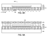
- FIGS. 8A to 8H illustrate manufacturing processes of the semiconductor package 100 of FIG. 1 .
- the carrier 180 may be formed by a metal plate comprising of copper, iron or steel.
- the first conductive layer 111 is formed on the carrier 180 using, for example, photolithography, electroless plating, electrolytic plating, printing, sputtering, vacuum deposition, etc.
- the first pillar layer 112 is formed on the first conductive layer 111 using, for example, photolithography, electroless plating, electrolytic plating, printing, sputtering, vacuum deposition, etc.
- the first package body 113 encapsulating the first conductive layer 111 and the first pillar layer 112 is formed on an upper surface 180u of the carrier 180.
- the first package body 113 may be formed by various packaging technologies, such as, for example, compression molding, injection molding, transfer molding or dispensing technology.
- the first package body 113 may be grinded, such that the first upper surface 1121 u of each pillar 1121 is exposed from the second upper surface 113u of the first package body 113, wherein the first upper surface 1121u is aligned with the second upper surface 113u.
- the second conductive layer 114 is formed on the first pillar layer 112 using, for example, photolithography, electroless plating, electrolytic plating, printing, sputtering, vacuum deposition, etc.
- the first conductive layer 111, the first pillar layer 112, the first package body 113 and the second conductive layer 114 form the package substrate 110.
- the first electronic component 120 is disposed on second conductive layer 114 of the package substrate 110 through the conductive contacts 121 using, for example, surface mount technology (SMT).
- SMT surface mount technology
- the second package body 130 encapsulating the first electronic component 120 and the second conductive layer 114 is formed on the package substrate 110.
- the second package body 130 may be formed by various packaging technologies, such as, for example, compression molding, injection molding, transfer molding or dispensing technology.
- the carrier 180 is removed using, for example, etching, peeling, etc. After the carrier 180 is removed, the first lower surface 1111 b of the first conductive layer 111 and the second lower surface 113b of the first package body 113 are exposed, wherein the first lower surface 1111 b and the second lower surface 113b are aligned with each other. For example, the first lower surface 1111 b and the second lower surface 113b are coplanar.
- the conductive contacts 150 are formed on the first lower surface 1111b of the first conductive layer 111 using, for example, ball mounting technology.
- the second electronic component 140 is disposed on the first lower surface 1111 b of the first conductive layer 111 using, for example, SMT.
- FIGS. 9A to 9B illustrate manufacturing processes of the semiconductor package 200 of FIG. 2 .
- the interposer 270 connects to the package substrate 110 through the second pillar layer 260.
- the interposer 270 may electrically connect to the first electronic component 120 through the second pillar layer 260 and the package substrate 110.
- the second package body 130 encapsulating the first electronic component 120, the second conductive layer 114 and second pillar layer 260 is formed between the package substrate 110 and the interposer 270.
- the second package body 130 may be formed by various packaging technologies, such as, for example, compression molding, injection molding, transfer molding or dispensing technology.
- the carrier 180 is removed.
- the first lower surface 1111 b of the first conductive layer 111 and the second lower surface 113b of the first package body 113 are exposed, wherein the first lower surface 1111b and the second lower surface 113b are aligned with each other.
- the first lower surface 1111 b and the second lower surface 113b are coplanar.
- the conductive contacts 150 and the second electronic component 140 are formed on the first lower surface 1111 b of the first conductive layer 111 to form the semiconductor package 200 of FIG. 2 .
- the third electronic component 11 of FIG. 6 may be disposed on the interposer 270 of FIG. 9B to form the semiconductor device 10 of FIG. 6 .
- FIGS. 10A to 10C illustrate manufacturing processes of the semiconductor package 300 of FIG. 3 .
- the fourth conductive layer 370 formed on a carrier 190 connects to the package substrate 110 through the second pillar layer 260.
- the fourth conductive layer 370 may electrically connect to the first electronic component 120 through the second pillar layer 260 and the package substrate 110.
- the second package body 130 encapsulating the first electronic component 120, the second conductive layer 114, the second pillar layer 260 and the fourth conductive layer 370 is formed between the package substrate 110 and the carrier 190.
- the second package body 130 may be formed by various packaging technologies, such as, for example, compression molding, injection molding, transfer molding or dispensing technology.
- the carrier 190 is removed to expose the fourth upper surface 130u of the second package body 130 and the fifth upper surface 371u of the fourth conductive layer 370, wherein the fourth upper surface 130u and the fifth upper surface 371 u are aligned with each other.
- the carrier 180 is removed. After the carrier 180 is removed, the first lower surface 1111b of the first conductive layer 111 and the second lower surface 113b of the first package body 113 are exposed, wherein the first lower surface 1111b and the second lower surface 113b are aligned with each other. For example, the first lower surface 1111 b and the second lower surface 113b are coplanar.
- the conductive contacts 150 and the second electronic component 140 are formed on the first lower surface 1111 b of the first conductive layer 111 to form the semiconductor package 300 of FIG. 3 .
- the third electronic component 11 of FIG. 7 may be disposed on the fourth conductive layer 370 of FIG. 10C to form the semiconductor device 20 of FIG. 7 .
- FIGS. 11A to 11H illustrate manufacturing processes of the semiconductor package 400 of FIG. 4 .
- the carrier 180 is provided.
- the carrier 180 may be formed by a metal plate comprising of copper, iron or steel.
- the first conductive layer 111, the first pillar layer 112, the first package body 113 are formed on the carrier 180 using the processes, as mentioned above.
- the third pillar layer 411 is formed on the first pillar layer 112 using, for example, photolithography, electroless plating, electrolytic plating, printing, sputtering, vacuum deposition, etc.
- the third pillar layer 412 is formed on the third pillar layer 411 using, for example, photolithography, electroless plating, electrolytic plating, printing, sputtering, vacuum deposition, etc.
- the third package body 413 encapsulating the third conductive layer 411 and the third pillar layer 412 is formed on the second upper surface 113u of the first package body 113.
- the third package body 413 may be formed by various packaging technologies, such as, for example, compression molding, injection molding, transfer molding or dispensing technology.
- the third package body 413 may be grinded, such that an upper surface 412u of the third pillar layer 412 is exposed from the sixth upper surface 413u of the third package body 413, wherein the upper surface 412u is aligned with the sixth upper surface 413u.
- the second conductive layer 114 is formed on the third pillar layer 412 using, for example, photolithography, electroless plating, electrolytic plating, printing, sputtering, vacuum deposition, etc.
- the first conductive layer 111, the first pillar layer 112, the first package body 113, the second conductive layer 114, the third conductive layer 411, the third pillar layer 412 and the third package body 413 form the package substrate 410.
- the first electronic component 120 is disposed on second conductive layer 114 of the package substrate 410 through the conductive contacts 121 using, for example, surface mount technology (SMT).
- SMT surface mount technology
- the interposer 270 connects to the package substrate 410 through the second pillar layer 260.
- the interposer 270 may electrically connect to the first electronic component 120 through the second pillar layer 260 and the package substrate 410.
- the second package body 130 encapsulating the first electronic component 120, the second conductive layer 114 and second pillar layer 260 is formed between the package substrate 410 and the interposer 270.
- the second package body 130 may be formed by various packaging technologies, such as, for example, compression molding, injection molding, transfer molding or dispensing technology.
- the carrier 180 is removed using, for example, etching, peeling, etc. After the carrier 180 is removed, the first lower surface 1111b of the first conductive layer 111 and the second lower surface 113b of the first package body 113 are exposed, wherein the first lower surface 1111b and the second lower surface 113b are aligned with each other. For example, the first lower surface 1111b and the second lower surface 113b are coplanar.
- the conductive contacts 150 and the second electronic component 140 are formed on the first lower surface 1111b of the first conductive layer 111 to form the semiconductor package 400 of FIG. 4 .
- the third electronic component 11 of FIG. 6 may be disposed on the interposer 270 of FIG. 11 H to form another semiconductor device.
- FIGS. 12A to 12C illustrate manufacturing processes of the semiconductor package 500 of FIG. 5 .
- the fourth conductive layer 370 formed on the carrier 190 connects to the package substrate 410 through the second pillar layer 260.
- the fourth conductive layer 370 may electrically connect to the first electronic component 120 through the second pillar layer 260 and the package substrate 410.
- the second package body 130 encapsulating the first electronic component 120, the second conductive layer 114, the second pillar layer 260 and the fourth conductive layer 370 is formed between the package substrate 410 and the carrier 190.
- the second package body 130 may be formed by various packaging technologies, such as, for example, compression molding, injection molding, transfer molding or dispensing technology.
- the carrier 190 is removed to expose the fourth upper surface 130u of the second package body 130 and the fifth upper surface 371u of the fourth conductive layer 370, wherein the fourth upper surface 130u and the fifth upper surface 371 u are aligned with each other.
- the carrier 180 is removed. After the carrier 180 is removed, the first lower surface 1111 b of the first conductive layer 111 and the second lower surface 113b of the first package body 113 are exposed, wherein the first lower surface 1111b and the second lower surface 113b are aligned with each other. For example, the first lower surface 1111 b and the second lower surface 113b are coplanar.
- the conductive contacts 150 and the second electronic component 140 are formed on the first lower surface 1111 b of the first conductive layer 111 to form the semiconductor package 500 of FIG. 5 .
- the third electronic component 11 of FIG. 7 may be disposed on the fourth conductive layer 370 of FIG. 12C to form another semiconductor device.
Landscapes
- Engineering & Computer Science (AREA)
- Structures For Mounting Electric Components On Printed Circuit Boards (AREA)
- Manufacturing & Machinery (AREA)
- Microelectronics & Electronic Packaging (AREA)
- Ceramic Engineering (AREA)
- Structures Or Materials For Encapsulating Or Coating Semiconductor Devices Or Solid State Devices (AREA)
- Encapsulation Of And Coatings For Semiconductor Or Solid State Devices (AREA)
- Physics & Mathematics (AREA)
- Geometry (AREA)
Abstract
Description
- The invention relates to a semiconductor package, a semiconductor device using the same and a manufacturing method thereof, and more particularly to a thin semiconductor package, a semiconductor device using the same and a manufacturing method thereof.
- In the electronics industry, high integration and multiple functions with high performance become essential for new products. And meanwhile, high integration may cause higher manufacturing cost, since the manufacturing cost is in proportional to its size. Therefore, demanding on miniaturization of integrated circuit (IC) packages has become more and more critical.
- Package-on-package (PoP) is now the fastest growing semiconductor package technology since it is a cost-effective solution to high-density system integration in a single package. In a PoP structure, various packages are integrated in a single semiconductor package to reduce the size. Accordingly, there exists a need to provide a semiconductor package to overcomes, or at least reduces the above-mentioned problems.
- Therefore, it is important to increase the performance of the 3D graphic processing circuit while reducing the consumption of the electric power and extending the operating time of the mobile device.
- In one embodiment of the invention, a semiconductor package is provided. The semiconductor package includes a package substrate, a first electronic component and a second package body. The package substrate includes a first conductive layer, a first pillar layer, a first package body and a second conductive layer, wherein the first pillar layer is formed on the first conductive layer, the first package body encapsulates the first conductive layer and the first pillar layer, and the second conductive layer electrically connects to the first pillar layer. The first electronic component is disposed above the second conductive layer of the package substrate. The second package body encapsulates the first electronic component and the second conductive layer.
- In another embodiment of the invention, a semiconductor device is provided. The semiconductor device includes a semiconductor package, a second pillar layer and a third electronic component. The semiconductor package includes a package substrate, a first electronic component and a second package body. The package substrate includes a first conductive layer, a first pillar layer, a first package body and a second conductive layer, wherein the first pillar layer is formed on the first conductive layer, the first package body encapsulates the first conductive layer and the first pillar layer, and the second conductive layer electrically connects to the first pillar layer. The first electronic component is disposed above the second conductive layer of the package substrate. The second package body encapsulates the first electronic component and the second conductive layer. The second pillar layer is formed on the second conductive layer of the semiconductor package. The third electronic component is disposed above the second package body and electrically connects to the package substrate through the second pillar layer. The second package body further encapsulates the second pillar layer.
- In another embodiment of the invention, a manufacturing method of a semiconductor package is provided. The manufacturing method includes the following steps. A carrier is provided; a package body is formed and includes the steps of forming a first conductive layer on the carrier, forming a first pillar layer on the first conductive layer, forming a first package body encapsulating the first conductive layer and the first pillar layer, and forming a second conductive layer on the first pillar layer; a first electronic component is disposed above the second conductive layer of the package substrate; a second package body encapsulating the first electronic component and the second conductive layer is formed, and the carrier is removed.
- In another embodiment of the invention, a manufacturing method of a semiconductor device is provided. The manufacturing method includes the following steps. A carrier is provided; a package body is formed and includes the steps of forming a first conductive layer on the carrier, forming a first pillar layer on the first conductive layer, forming a first package body encapsulating the first conductive layer and the first pillar layer, and forming a second conductive layer on the first pillar layer; a first electronic component is disposed above the second conductive layer of the package substrate; a second package body encapsulating the first electronic component, the second conductive layer and the second pillar layer is formed, and the carrier is removed.
- Numerous objects, features and advantages of the invention will be readily apparent upon a reading of the following detailed description of embodiments of the invention when taken in conjunction with the accompanying drawings. However, the drawings employed herein are for the purpose of descriptions and should not be regarded as limiting.
- The above objects and advantages of the invention will become more readily apparent to those ordinarily skilled in the art after reviewing the following detailed description and accompanying drawings, in which:
-
FIG. 1 illustrates a diagram of a semiconductor package according to an embodiment of the invention; -
FIG. 2 illustrates a diagram of a semiconductor package according to another embodiment of the invention; -
FIG. 3 illustrates a diagram of a semiconductor package according to another embodiment of the invention; -
FIG. 4 illustrates a diagram of a semiconductor package according to another embodiment of the invention; -
FIG. 5 illustrates a diagram of a semiconductor package according to another embodiment of the invention; -
FIG. 6 illustrates a diagram of a semiconductor device according to one embodiment of the invention; -
FIG. 7 illustrates a diagram of a semiconductor device according to another embodiment of the invention; -
FIGS. 8A to 8H illustrate manufacturing processes of the semiconductor package ofFIG. 1 ; -
FIGS. 9A to 9B illustrate manufacturing processes of the semiconductor package ofFIG. 2 ; -
FIGS. 10A to 10C illustrate manufacturing processes of the semiconductor package ofFIG. 3 ; -
FIGS. 11A to 11 H illustrate manufacturing processes of the semiconductor package ofFIG. 4 ; and -
FIGS. 12A to 12C illustrate manufacturing processes of the semiconductor package ofFIG. 5 . -
FIG. 1 illustrates a diagram of asemiconductor package 100 according to an embodiment of the invention. Thesemiconductor package 100 includes apackage substrate 110, a firstelectronic component 120, asecond package body 130, a secondelectronic component 140 and at least oneconductive contact 150. - The
package substrate 110 includes a firstconductive layer 111, afirst pillar layer 112, afirst package body 113 and a secondconductive layer 114. - The first
conductive layer 111 includes a plurality ofelements 1111, such as pads, traces or combination thereof. Eachelement 1111 has a firstlower surface 1111 b and a firstlateral surface 1111 s, and thefirst package body 113 has a secondlower surface 113b. The firstlower surface 1111 b is exposed from the secondlower surface 113b, and the firstlower surface 1111 b is aligned with the secondlower surface 113b. Eachelement 1111 may be a multi-layered structure or single-layered structure. For example, eachelement 1111 includes nickel layer, gold layer, palladium layer, copper layer or combination thereof. - The
first pillar layer 112 connects the firstconductive layer 111 to the secondconductive layer 114. In the present embodiment, thefirst pillar layer 112 includes a plurality ofpillars 1121. Thepillars 1121 are made of a material such as copper. Eachpillar 1121 has a firstupper surface 1121 u, and thefirst package body 113 has a secondupper surface 113u, wherein the firstupper surface 1121u is exposed from the secondupper surface 113u and aligned with the secondupper surface 113u. - The
first package body 113 encapsulates the firstconductive layer 111 and thefirst pillar layer 112. For example, thefirst package body 113 encapsulates the firstlateral surface 1111 s of the firstconductive layer 111 and the lateral surface of eachpillar 1121. - The
first package body 113 may be a molding compound which is made of a material including, for example, a Novolac-based resin, an epoxy-based resin, a silicone-based resin, or another suitable encapsulant. Suitable fillers also can be included, such as powdered SiO2. - Since the
first package body 113 is the molding compound, thepackage substrate 110 has thin thickness t1. Compared to the silicon substrate, the thickness t1 of thepackage substrate 110 is much smaller. In general, the silicon substrate has a thickness larger than 100 micrometers. In the present embodiment, the thickness t1 of thepackage substrate 110 is smaller, and accordingly the thickness t2 of thesemiconductor package 100 may be reduced. - The second
conductive layer 114 includes a plurality ofelements 1141, such as pads, traces or combination thereof. Eachelement 1141 may be a multi-layered structure or single-layered structure. For example, theelement 1141 may be nickel layer, gold layer, copper layer, palladium layer or combination thereof. - In the present embodiment, the first
electronic component 120 is coupled to the secondconductive layer 114 of thepackage substrate 110 in a "face-down" orientation and electrically connected to the secondconductive layer 114 via a plurality ofconductive contacts 121. This configuration is sometimes referred to as "flip-chip". Theconductive contact 121 may be solder ball, conductive pillar, etc. - In other embodiments, the first
electronic component 120 may be coupled to thepackage substrate 110 in a "face-up" orientation, and electrically connected to thepackage substrate 110 via a plurality of conductive bond wires (not shown). The firstelectronic component 120 may be an active chip or a passive component, such as a resistor, an inductor or a capacitor. In another embodiment, the number of the firstelectronic component 120 may be several. In addition, the firstelectronic component 120 may be, for example, a chip, a passive component, etc. - The
second package body 130 formed on the secondupper surface 113u of thepackage substrate 110 encapsulates the secondconductive layer 114 and the firstelectronic component 120. Thesecond package body 130 may be made of a material which is the same as that of thefirst package body 113. - The second
electronic component 140 is disposed on the firstlower surface 1111 b of thefirst substrate 110 and electrically connects to the firstconductive layer 111. In one embodiment, the secondelectronic component 140 is, for example, passive component, such as a resistor, an inductor or a capacitor. - The
conductive contacts 150 are disposed on the firstlower surface 1111 b of thefirst substrate 110. Thesemiconductor package 100 is disposed on and electrically connected to an exterior circuit, such as a circuit board, through theconductive contacts 150. Theconductive contacts 150 may be solder ball, conductive pillar, etc. -
FIG. 2 illustrates a diagram of asemiconductor package 200 according to another embodiment of the invention. Thesemiconductor package 200 includes thepackage substrate 110, the firstelectronic component 120, thesecond package body 130, the secondelectronic component 140, at least oneconductive contact 150, asecond pillar layer 260 and aninterposer 270. - The
second package body 130 further encapsulates thesecond pillar layer 260. Thesecond pillar layer 260 includes a plurality ofpillars 261 connecting the secondconductive layer 114 to theinterposer 270. - The
interposer 270 is disposed on thesecond package body 130 and electrically connects to thepackage substrate 110 through thesecond pillar layer 260 encapsulated withinsecond package body 130. Theinterposer 270 may be electrically connected to the firstelectronic component 120 through thesecond pillar layer 260 and thepackage substrate 110. - Each
pillar 261 has a thirdupper surface 261 u, and thesecond package body 130 has a fourthupper surface 130u, wherein the thirdupper surface 261 u is exposed from the fourthupper surface 130u and aligned with the fourthupper surface 130u. -
FIG. 3 illustrates a diagram of asemiconductor package 300 according to another embodiment of the invention. Thesemiconductor package 300 includes thepackage substrate 110, the firstelectronic component 120, thesecond package body 130, the secondelectronic component 140, at least oneconductive contact 150, thesecond pillar layer 260 and a fourthconductive layer 370. - The
second package body 130 encapsulates the secondconductive layer 114, thesecond pillar layer 260 and the fourthconductive layer 370. - The
second pillar layer 260 electrically connects the secondconductive layer 114 to the fourthconductive layer 370, such that the firstelectronic component 120 may electrically connect the fourthconductive layer 370 through thepackage substrate 110 and thesecond pillar layer 260. - The fourth
conductive layer 370 includes a plurality ofelements 371, such as pads, traces or combination thereof. Eachelement 371 has a fifthupper surface 371 u, and thesecond package body 130 has the fourthupper surface 130u, wherein the fifthupper surface 371 u is exposed from the fourthupper surface 130u and aligned with the fourthupper surface 130u. - Each
element 371 may be a multi-layered structure or single-layered structure. For example, the eachelement 371 includes nickel layer, gold layer, palladium layer, copper layer or combination thereof. - The fourth
conductive layer 370 is embedded in thesecond package body 130. For example, each element 371 (trace or pad) has a secondlateral surface 371 s which is encapsulated by thesecond package body 130. Since the fourthconductive layer 370 is embedded in thesecond package body 130, thesecond package body 130 has a thin thickness t3. -
FIG. 4 illustrates a diagram of asemiconductor package 400 according to another embodiment of the invention. Thesemiconductor package 400 includes apackage substrate 410, the firstelectronic component 120, thesecond package body 130, the secondelectronic component 140, at least oneconductive contact 150, thesecond pillar layer 260 and theinterposer 270. - In the present embodiment, the
package substrate 410 is multi-layered package structure. For example, thepackage substrate 410 includes the firstconductive layer 111, thefirst pillar layer 112, thefirst package body 113, the secondconductive layer 114, a thirdconductive layer 411, athird pillar layer 412 and athird package body 413. The firstconductive layer 111, thefirst pillar layer 112 and thefirst package body 113 together form a first single-layered package structure, and the thirdconductive layer 411, thethird pillar layer 412 and thethird package body 413 form a second single-layered package structure. In another embodiment, the number of the layers of thepackage substrate 410 may be more than two. - The third
conductive layer 411 is formed on the secondupper surface 113u of thefirst package body 113 and electrical connects to thefirst pillar layer 112. Thethird pillar layer 412 connects the thirdconductive layer 411 to the secondconductive layer 114. Thethird package body 413 encapsulates thethird pillar layer 412 and the thirdconductive layer 411. In the present embodiment, the secondconductive layer 114 is formed on a sixthupper surface 413u of thethird package body 413 and electrically connects to the firstconductive layer 111 through the thirdconductive layer 411, thethird pillar layer 412 and thefirst pillar layer 112. - In addition, the
third package body 413 may be made of a material which is the same as that of thefirst package body 113. - Since the
first package body 113 and thethird package body 413 are the molding compounds, thepackage substrate 410 has thin thickness t1. Compared to the silicon substrate, the thickness t1 of thepackage substrate 410 is much smaller. In general, the silicon substrate has the thickness larger than 100 micrometers. In the present embodiment, the thickness t1 of thepackage substrate 410 is smaller, and accordingly the thickness t2 of thesemiconductor package 100 may be reduced. -
FIG. 5 illustrates a diagram of asemiconductor package 500 according to another embodiment of the invention. Thesemiconductor package 500 includes thepackage substrate 410, the firstelectronic component 120, thesecond package body 130, the secondelectronic component 140, at least oneconductive contact 150, thesecond pillar layer 260 and the fourthconductive layer 370. - In the present embodiment, since the fourth
conductive layer 370 is embedded in thesecond package body 130, thesecond package body 130 has the thin thickness t3. Thesecond pillar layer 260 electrically connects the secondconductive layer 114 to the fourthconductive layer 370, such that the firstelectronic component 120 may electrically connect the fourthconductive layer 370 through thepackage substrate 410 and thesecond pillar layer 260. -
FIG. 6 illustrates a diagram of asemiconductor device 10 according to one embodiment of the invention. Thesemiconductor device 10 includes thesemiconductor package 200 and a thirdelectronic component 11. In another embodiment, the thirdelectronic component 11 may be a semiconductor package including a plurality of dies, such as DRAMs stacked to each other. - The third
electronic component 11 is disposed on theinterposer 270 of thesemiconductor package 200 in a "face-down" orientation and electrically connected to theinterposer 270 via a plurality ofconductive contacts 115. Theconductive contacts 115 may be solder ball, conductive pillar, etc. In another embodiment, the thirdelectronic component 11 is disposed on theinterposer 270 in a "face-up" orientation and electrically connected to theinterposer 270 via a plurality of conductive bond wires (not shown). The thirdelectronic component 11 electrically connects to the firstelectronic component 120 through theinterposer 270, thesecond pillar layer 260 and thepackage substrate 110. In addition, the thirdelectronic component 11 electrically connects to theconductive contacts 150 through theinterposer 270, thesecond pillar layer 260 and thepackage substrate 110. -
FIG. 7 illustrates a diagram of asemiconductor device 20 according to another embodiment of the invention. Thesemiconductor device 20 includes thesemiconductor package 300 and a thirdelectronic component 11. - The third
electronic component 11 is disposed on the fourthconductive layer 370 of thesemiconductor package 300 in a "face-down" orientation or in a "face-up" orientation. The thirdelectronic component 11 electrically connects to the firstelectronic component 120 through the fourthconductive layer 370, thesecond pillar layer 260 and thepackage substrate 110. In addition, the thirdelectronic component 11 electrically connects to theconductive contacts 150 through the fourthconductive layer 370, thesecond pillar layer 260 and thepackage substrate 110. - In another embodiment, the third
electronic component 11 may be disposed on theinterposer 270 of thesemiconductor package 400 ofFIG. 4 to form another semiconductor device. In other embodiment, the thirdelectronic component 11 may be disposed on the fourthconductive layer 370 of thesemiconductor package 500 ofFIG. 5 to form another semiconductor device. -
FIGS. 8A to 8H illustrate manufacturing processes of thesemiconductor package 100 ofFIG. 1 . - Referring to
FIG. 8A , acarrier 180 is provided. Thecarrier 180 may be formed by a metal plate comprising of copper, iron or steel. - Referring to
FIG. 8A , the firstconductive layer 111 is formed on thecarrier 180 using, for example, photolithography, electroless plating, electrolytic plating, printing, sputtering, vacuum deposition, etc. - Referring to
FIG. 8B , thefirst pillar layer 112 is formed on the firstconductive layer 111 using, for example, photolithography, electroless plating, electrolytic plating, printing, sputtering, vacuum deposition, etc. - Referring to
FIG. 8C , thefirst package body 113 encapsulating the firstconductive layer 111 and thefirst pillar layer 112 is formed on anupper surface 180u of thecarrier 180. Thefirst package body 113 may be formed by various packaging technologies, such as, for example, compression molding, injection molding, transfer molding or dispensing technology. - In the present embodiment, the
first package body 113 may be grinded, such that the firstupper surface 1121 u of eachpillar 1121 is exposed from the secondupper surface 113u of thefirst package body 113, wherein the firstupper surface 1121u is aligned with the secondupper surface 113u. - Referring to
FIG. 8D , the secondconductive layer 114 is formed on thefirst pillar layer 112 using, for example, photolithography, electroless plating, electrolytic plating, printing, sputtering, vacuum deposition, etc. The firstconductive layer 111, thefirst pillar layer 112, thefirst package body 113 and the secondconductive layer 114 form thepackage substrate 110. - Referring to
FIG. 8E , the firstelectronic component 120 is disposed on secondconductive layer 114 of thepackage substrate 110 through theconductive contacts 121 using, for example, surface mount technology (SMT). - Referring to
FIG. 8F , thesecond package body 130 encapsulating the firstelectronic component 120 and the secondconductive layer 114 is formed on thepackage substrate 110. Thesecond package body 130 may be formed by various packaging technologies, such as, for example, compression molding, injection molding, transfer molding or dispensing technology. - Referring to
FIG. 8G , thecarrier 180 is removed using, for example, etching, peeling, etc. After thecarrier 180 is removed, the firstlower surface 1111 b of the firstconductive layer 111 and the secondlower surface 113b of thefirst package body 113 are exposed, wherein the firstlower surface 1111 b and the secondlower surface 113b are aligned with each other. For example, the firstlower surface 1111 b and the secondlower surface 113b are coplanar. - Referring to
FIG. 8H , theconductive contacts 150 are formed on the firstlower surface 1111b of the firstconductive layer 111 using, for example, ball mounting technology. In addition, the secondelectronic component 140 is disposed on the firstlower surface 1111 b of the firstconductive layer 111 using, for example, SMT. -
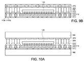
FIGS. 9A to 9B illustrate manufacturing processes of thesemiconductor package 200 ofFIG. 2 . - Referring to
FIG. 9A , theinterposer 270 connects to thepackage substrate 110 through thesecond pillar layer 260. Theinterposer 270 may electrically connect to the firstelectronic component 120 through thesecond pillar layer 260 and thepackage substrate 110. - Referring to
FIG. 9B , thesecond package body 130 encapsulating the firstelectronic component 120, the secondconductive layer 114 andsecond pillar layer 260 is formed between thepackage substrate 110 and theinterposer 270. Thesecond package body 130 may be formed by various packaging technologies, such as, for example, compression molding, injection molding, transfer molding or dispensing technology. - Then, referring to
FIG. 9B , thecarrier 180 is removed. After thecarrier 180 is removed, the firstlower surface 1111 b of the firstconductive layer 111 and the secondlower surface 113b of thefirst package body 113 are exposed, wherein the firstlower surface 1111b and the secondlower surface 113b are aligned with each other. For example, the firstlower surface 1111 b and the secondlower surface 113b are coplanar. - Then, the
conductive contacts 150 and the secondelectronic component 140 are formed on the firstlower surface 1111 b of the firstconductive layer 111 to form thesemiconductor package 200 ofFIG. 2 . - In another embodiment, the third
electronic component 11 ofFIG. 6 may be disposed on theinterposer 270 ofFIG. 9B to form thesemiconductor device 10 ofFIG. 6 . -
FIGS. 10A to 10C illustrate manufacturing processes of thesemiconductor package 300 ofFIG. 3 . - Referring to
FIG. 10A , the fourthconductive layer 370 formed on acarrier 190 connects to thepackage substrate 110 through thesecond pillar layer 260. The fourthconductive layer 370 may electrically connect to the firstelectronic component 120 through thesecond pillar layer 260 and thepackage substrate 110. - Referring to
FIG. 10B , thesecond package body 130 encapsulating the firstelectronic component 120, the secondconductive layer 114, thesecond pillar layer 260 and the fourthconductive layer 370 is formed between thepackage substrate 110 and thecarrier 190. Thesecond package body 130 may be formed by various packaging technologies, such as, for example, compression molding, injection molding, transfer molding or dispensing technology. - Referring to
FIG. 10C , thecarrier 190 is removed to expose the fourthupper surface 130u of thesecond package body 130 and the fifthupper surface 371u of the fourthconductive layer 370, wherein the fourthupper surface 130u and the fifthupper surface 371 u are aligned with each other. - Referring to
FIG. 10C , thecarrier 180 is removed. After thecarrier 180 is removed, the firstlower surface 1111b of the firstconductive layer 111 and the secondlower surface 113b of thefirst package body 113 are exposed, wherein the firstlower surface 1111b and the secondlower surface 113b are aligned with each other. For example, the firstlower surface 1111 b and the secondlower surface 113b are coplanar. - Then, the
conductive contacts 150 and the secondelectronic component 140 are formed on the firstlower surface 1111 b of the firstconductive layer 111 to form thesemiconductor package 300 ofFIG. 3 . - In another embodiment, the third
electronic component 11 ofFIG. 7 may be disposed on the fourthconductive layer 370 ofFIG. 10C to form thesemiconductor device 20 ofFIG. 7 . -
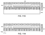
FIGS. 11A to 11H illustrate manufacturing processes of thesemiconductor package 400 ofFIG. 4 . - Referring to
FIG. 11 A , thecarrier 180 is provided. Thecarrier 180 may be formed by a metal plate comprising of copper, iron or steel. - Referring to
FIG. 11A , the firstconductive layer 111, thefirst pillar layer 112, thefirst package body 113 are formed on thecarrier 180 using the processes, as mentioned above. - Referring to
FIG. 11 B , thethird pillar layer 411 is formed on thefirst pillar layer 112 using, for example, photolithography, electroless plating, electrolytic plating, printing, sputtering, vacuum deposition, etc. - Referring to
FIG. 11B , thethird pillar layer 412 is formed on thethird pillar layer 411 using, for example, photolithography, electroless plating, electrolytic plating, printing, sputtering, vacuum deposition, etc. - Referring to
FIG. 11C , thethird package body 413 encapsulating the thirdconductive layer 411 and thethird pillar layer 412 is formed on the secondupper surface 113u of thefirst package body 113. Thethird package body 413 may be formed by various packaging technologies, such as, for example, compression molding, injection molding, transfer molding or dispensing technology. - In the present embodiment, the
third package body 413 may be grinded, such that anupper surface 412u of thethird pillar layer 412 is exposed from the sixthupper surface 413u of thethird package body 413, wherein theupper surface 412u is aligned with the sixthupper surface 413u. - Referring to
FIG. 11 D , the secondconductive layer 114 is formed on thethird pillar layer 412 using, for example, photolithography, electroless plating, electrolytic plating, printing, sputtering, vacuum deposition, etc. The firstconductive layer 111, thefirst pillar layer 112, thefirst package body 113, the secondconductive layer 114, the thirdconductive layer 411, thethird pillar layer 412 and thethird package body 413 form thepackage substrate 410. - Referring to
FIG. 11E , the firstelectronic component 120 is disposed on secondconductive layer 114 of thepackage substrate 410 through theconductive contacts 121 using, for example, surface mount technology (SMT). - Referring to
FIG. 11 F , theinterposer 270 connects to thepackage substrate 410 through thesecond pillar layer 260. Theinterposer 270 may electrically connect to the firstelectronic component 120 through thesecond pillar layer 260 and thepackage substrate 410. - Referring to
FIG. 11G , thesecond package body 130 encapsulating the firstelectronic component 120, the secondconductive layer 114 andsecond pillar layer 260 is formed between thepackage substrate 410 and theinterposer 270. Thesecond package body 130 may be formed by various packaging technologies, such as, for example, compression molding, injection molding, transfer molding or dispensing technology. - Referring to
FIG. 11 H , thecarrier 180 is removed using, for example, etching, peeling, etc. After thecarrier 180 is removed, the firstlower surface 1111b of the firstconductive layer 111 and the secondlower surface 113b of thefirst package body 113 are exposed, wherein the firstlower surface 1111b and the secondlower surface 113b are aligned with each other. For example, the firstlower surface 1111b and the secondlower surface 113b are coplanar. - Then, the
conductive contacts 150 and the secondelectronic component 140 are formed on the firstlower surface 1111b of the firstconductive layer 111 to form thesemiconductor package 400 ofFIG. 4 . - In another embodiment, the third
electronic component 11 ofFIG. 6 may be disposed on theinterposer 270 ofFIG. 11 H to form another semiconductor device. -
FIGS. 12A to 12C illustrate manufacturing processes of thesemiconductor package 500 ofFIG. 5 . - Referring to
FIG. 12A , the fourthconductive layer 370 formed on thecarrier 190 connects to thepackage substrate 410 through thesecond pillar layer 260. The fourthconductive layer 370 may electrically connect to the firstelectronic component 120 through thesecond pillar layer 260 and thepackage substrate 410. - Referring to
FIG. 12B , thesecond package body 130 encapsulating the firstelectronic component 120, the secondconductive layer 114, thesecond pillar layer 260 and the fourthconductive layer 370 is formed between thepackage substrate 410 and thecarrier 190. Thesecond package body 130 may be formed by various packaging technologies, such as, for example, compression molding, injection molding, transfer molding or dispensing technology. - Referring to
FIG. 12C , thecarrier 190 is removed to expose the fourthupper surface 130u of thesecond package body 130 and the fifthupper surface 371u of the fourthconductive layer 370, wherein the fourthupper surface 130u and the fifthupper surface 371 u are aligned with each other. - Referring to
FIG. 12C , thecarrier 180 is removed. After thecarrier 180 is removed, the firstlower surface 1111 b of the firstconductive layer 111 and the secondlower surface 113b of thefirst package body 113 are exposed, wherein the firstlower surface 1111b and the secondlower surface 113b are aligned with each other. For example, the firstlower surface 1111 b and the secondlower surface 113b are coplanar. - Then, the
conductive contacts 150 and the secondelectronic component 140 are formed on the firstlower surface 1111 b of the firstconductive layer 111 to form thesemiconductor package 500 ofFIG. 5 . - In another embodiment, the third
electronic component 11 ofFIG. 7 may be disposed on the fourthconductive layer 370 ofFIG. 12C to form another semiconductor device. - While the invention has been described in terms of what is presently considered to be the most practical and preferred embodiments, it is to be understood that the invention needs not be limited to the disclosed embodiment. On the contrary, it is intended to cover various modifications and similar arrangements included within the spirit and scope of the appended claims which are to be accorded with the broadest interpretation so as to encompass all such modifications and similar structures.
Claims (15)
- A semiconductor package (100-500), comprising:a package substrate (110, 410), which comprises:a first conductive layer (111);a first pillar layer (112) formed on the first conductive layer (111);a first package body (113) encapsulating the first conductive layer (111) and the first pillar layer (112); anda second conductive layer (114) electrically connecting to the first pillar layer (112);a first electronic component (120) disposed above the second conductive layer (114) of the package substrate (110, 410); anda second package body (130) encapsulating the first electronic component (120) and the second conductive layer (114).
- The semiconductor package (100-500) as claimed in claim 1, being characterized in that the first package body (113) is molding compound.
- The semiconductor package (100-500) as claimed in claim 1 or 2, being characterized in that the semiconductor package (100-500) further comprises:a second pillar layer (260) formed on the second conductive layer (114);wherein the second package body (130) further encapsulates the second pillar layer (260).
- The semiconductor package (100-500) as claimed in any one of the claims 1 to 3, being characterized in that the package substrate (110, 410) further comprises:a third conductive layer (411) formed on the first package body (113);a third pillar layer (412) connecting the third conductive layer (411) to the second conductive layer (114); anda third package body (413) encapsulating the third pillar layer (412) and the third conductive layer (411);wherein the second conductive layer (114) is formed on the third package body (413).
- The semiconductor package (100-500) as claimed in claim 4, being characterized in that the third package body (413) is molding compound.
- The semiconductor package (100-500) as claimed in any one of the claims 1 to 5, being characterized in that the first conductive layer (111) has a first lower surface (1111 b), the first package body (113) has a second lower surface (113b), the first lower surface (1111 b) is exposed form the second lower surface (113b), and the semiconductor package (100-500) further comprises:a second electronic component (140) disposed on the first lower surface (1111b) of the first conductive layer (111).
- The semiconductor package (100-500) as claimed in any one of the claims 1 to 6, being characterized in that semiconductor package (100-500) further comprises:an interposer (270) disposed on the second package body (130) and electrically connecting to the package substrate (110, 410).
- The semiconductor package (100-500) as claimed in any one of the claims 1 to 7, being characterized in that semiconductor package (100-500) further comprises:a fourth conductive layer (370); anda second pillar layer (260) connecting the fourth conductive layer (370) to the second conductive layer (114);wherein the second package body (130) encapsulates the second pillar layer (260) and the fourth conductive layer (370).
- The semiconductor package (100-500) as claimed in any one of the claims 1 to 8, being characterized in that the first pillar layer (112) has a first upper surface, the first package body (113) has a second upper surface (113u), and the first upper surface is aligned with the second upper surface (113u).
- The semiconductor package (100-500) as claimed in any one of the claims 1 to 9, being characterized in that the first conductive layer (111) has a first lower surface (1111 b), the first package body (113) has a second lower surface (113b), and the first lower surface (1111 b) is aligned with the second lower surface (113b).
- A semiconductor device, comprising:a semiconductor package (100-500) as claimed in any of the claims 1 to 10;a second pillar layer (260) formed on the second conductive layer (114) of the semiconductor package (100-500); anda third electronic component (11) disposed above the second package body (130) and electrically connecting to the package substrate (110, 410) through the second pillar layer (260);wherein the second package body (130) further encapsulates the second pillar layer (260).
- The semiconductor device as claimed in claim 11, being characterized in that semiconductor device further comprises:an interposer (270) disposed on the second package body (130) and electrically connecting to the package substrate (110, 410) through the second pillar layer (260);wherein the third electronic component (11) is disposed on and electrically to the interposer (270).
- The semiconductor device as claimed in claim 11 or 12, being characterized in that semiconductor device further comprises:a fourth conductive layer (370);wherein the second pillar layer (260) connects the fourth conductive layer (370) to the second conductive layer (114), the second package body (130) encapsulates the second pillar layer (260) and the fourth conductive layer (370), and the third electronic component (11) is disposed on and electrically to the fourth conductive layer (370).
- A manufacturing method of a semiconductor package (100-500), the method comprising:providing a carrier (180);forming a package substrate (110, 410), comprising:forming a first conductive layer (111) on the carrier (180);forming a first pillar layer (112) on the first conductive layer (111);forming a first package body (113) encapsulating the first conductive layer (111) and the first pillar layer (112); andforming a second conductive layer (114) on the first pillar layer (112);disposing a first electronic component (120) above the second conductive layer (114) of the package substrate (110, 410);forming a second package body (130) encapsulating the first electronic component (120) and the second conductive layer (114); andremoving the carrier (180).
- A manufacturing method of a semiconductor device, the method comprising:providing a carrier (180);forming a package substrate, comprising:forming a first conductive layer (111) on the carrier (180);forming a first pillar layer (112) on the first conductive layer (111);forming a first package body (113) encapsulating the first conductive layer (111) and the first pillar layer (112); andforming a second conductive layer (114) on the first pillar layer (112);disposing a first electronic component (120) above the second conductive layer (114) of the package substrate (110, 410);connecting a second pillar layer (260) to the package substrate (110, 410);forming a second package body (130) encapsulating the first electronic component (120), the second conductive layer (114) and the second pillar layer (260);removing the carrier (180);disposing a third electronic component (11) above the second package body (130), wherein the third electronic component (11) electrically connects to the package substrate (110, 410) through the second pillar layer (260).
Applications Claiming Priority (2)
| Application Number | Priority Date | Filing Date | Title |
|---|---|---|---|
| US201562221262P | 2015-09-21 | 2015-09-21 | |
| US15/162,760 US9761534B2 (en) | 2015-09-21 | 2016-05-24 | Semiconductor package, semiconductor device using the same and manufacturing method thereof |
Publications (2)
| Publication Number | Publication Date |
|---|---|
| EP3147942A1 true EP3147942A1 (en) | 2017-03-29 |
| EP3147942B1 EP3147942B1 (en) | 2020-09-09 |
Family
ID=56203205
Family Applications (1)
| Application Number | Title | Priority Date | Filing Date |
|---|---|---|---|
| EP16175721.6A Active EP3147942B1 (en) | 2015-09-21 | 2016-06-22 | Semiconductor package, semiconductor device using the same and manufacturing method thereof |
Country Status (4)
| Country | Link |
|---|---|
| US (2) | US9761534B2 (en) |
| EP (1) | EP3147942B1 (en) |
| CN (1) | CN106548991A (en) |
| TW (1) | TWI595605B (en) |
Cited By (2)
| Publication number | Priority date | Publication date | Assignee | Title |
|---|---|---|---|---|
| EP3486943A1 (en) * | 2017-11-17 | 2019-05-22 | MediaTek Inc | Semiconductor package |
| US10784206B2 (en) | 2015-09-21 | 2020-09-22 | Mediatek Inc. | Semiconductor package |
Families Citing this family (11)
| Publication number | Priority date | Publication date | Assignee | Title |
|---|---|---|---|---|
| KR101672640B1 (en) * | 2015-06-23 | 2016-11-03 | 앰코 테크놀로지 코리아 주식회사 | Semiconductor device |
| US9761534B2 (en) | 2015-09-21 | 2017-09-12 | Mediatek Inc. | Semiconductor package, semiconductor device using the same and manufacturing method thereof |
| US10062626B2 (en) | 2016-07-26 | 2018-08-28 | Amkor Technology, Inc. | Semiconductor device and manufacturing method thereof |
| US10672741B2 (en) * | 2016-08-18 | 2020-06-02 | Taiwan Semiconductor Manufacturing Company, Ltd. | Semiconductor packages with thermal-electrical-mechanical chips and methods of forming the same |
| US10256114B2 (en) * | 2017-03-23 | 2019-04-09 | Amkor Technology, Inc. | Semiconductor device with tiered pillar and manufacturing method thereof |
| US11430739B2 (en) * | 2018-10-30 | 2022-08-30 | Taiwan Semiconductor Manufacturing Co., Ltd. | Structure and formation method of package structure with fan-out structure |
| US11201110B2 (en) * | 2019-07-31 | 2021-12-14 | Advanced Semiconductor Engineering, Inc. | Semiconductor device package with conductive pillars and method for manufacturing the same |
| US12500148B2 (en) | 2021-07-30 | 2025-12-16 | Stmicroelectronics S.R.L. | Method of coupling semiconductor dice, tool for use therein and corresponding semiconductor device |
| US12525512B2 (en) * | 2021-07-30 | 2026-01-13 | Stmicroelectronics S.R.L. | Method of coupling semiconductor dice and corresponding semiconductor device |
| US12482715B2 (en) * | 2022-11-28 | 2025-11-25 | Xilinx, Inc. | Chip package with core embedded integrated passive device |
| CN118299277A (en) * | 2023-01-05 | 2024-07-05 | 星科金朋私人有限公司 | Semiconductor device and method for manufacturing the same |
Citations (3)
| Publication number | Priority date | Publication date | Assignee | Title |
|---|---|---|---|---|
| US20110140259A1 (en) * | 2009-12-16 | 2011-06-16 | Cho Namju | Integrated circuit packaging system with stacking interconnect and method of manufacture thereof |
| US20120061814A1 (en) * | 2010-09-14 | 2012-03-15 | Stats Chippac, Ltd. | Semiconductor Device and Method of Forming Leadframe Interposer Over Semiconductor Die and TSV Substrate for Vertical Electrical Interconnect |
| US20140252646A1 (en) * | 2013-03-06 | 2014-09-11 | Taiwan Semiconductor Manufacturing Company, Ltd. | Interconnect Structure for Package-on-Package Devices |
Family Cites Families (13)
| Publication number | Priority date | Publication date | Assignee | Title |
|---|---|---|---|---|
| JP4787559B2 (en) * | 2005-07-26 | 2011-10-05 | ルネサスエレクトロニクス株式会社 | Semiconductor device and manufacturing method thereof |
| US7759212B2 (en) * | 2007-12-26 | 2010-07-20 | Stats Chippac, Ltd. | System-in-package having integrated passive devices and method therefor |
| US7858441B2 (en) * | 2008-12-08 | 2010-12-28 | Stats Chippac, Ltd. | Semiconductor package with semiconductor core structure and method of forming same |
| US9355962B2 (en) * | 2009-06-12 | 2016-05-31 | Stats Chippac Ltd. | Integrated circuit package stacking system with redistribution and method of manufacture thereof |
| US8716873B2 (en) | 2010-07-01 | 2014-05-06 | United Test And Assembly Center Ltd. | Semiconductor packages and methods of packaging semiconductor devices |
| US8080445B1 (en) * | 2010-09-07 | 2011-12-20 | Stats Chippac, Ltd. | Semiconductor device and method of forming WLP with semiconductor die embedded within penetrable encapsulant between TSV interposers |
| US8884431B2 (en) | 2011-09-09 | 2014-11-11 | Taiwan Semiconductor Manufacturing Company, Ltd. | Packaging methods and structures for semiconductor devices |
| US9049791B2 (en) * | 2013-06-07 | 2015-06-02 | Zhuhai Advanced Chip Carriers & Electronic Substrates Solutions Technologies Co. Ltd. | Terminations and couplings between chips and substrates |
| TWI534963B (en) * | 2014-02-14 | 2016-05-21 | 恆勁科技股份有限公司 | Packaging device and manufacturing method thereof |
| US9034694B1 (en) * | 2014-02-27 | 2015-05-19 | Freescale Semiconductor, Inc. | Embedded die ball grid array package |
| KR102198858B1 (en) * | 2014-07-24 | 2021-01-05 | 삼성전자 주식회사 | Semiconductor package stack structure having interposer substrate |
| US10354974B2 (en) | 2014-12-11 | 2019-07-16 | Mediatek Inc. | Structure and formation method of chip package structure |
| US9761534B2 (en) | 2015-09-21 | 2017-09-12 | Mediatek Inc. | Semiconductor package, semiconductor device using the same and manufacturing method thereof |
-
2016
- 2016-05-24 US US15/162,760 patent/US9761534B2/en active Active
- 2016-06-22 EP EP16175721.6A patent/EP3147942B1/en active Active
- 2016-06-28 TW TW105120336A patent/TWI595605B/en active
- 2016-07-29 CN CN201610614954.0A patent/CN106548991A/en active Pending
-
2017
- 2017-08-09 US US15/672,440 patent/US10186488B2/en active Active
Patent Citations (3)
| Publication number | Priority date | Publication date | Assignee | Title |
|---|---|---|---|---|
| US20110140259A1 (en) * | 2009-12-16 | 2011-06-16 | Cho Namju | Integrated circuit packaging system with stacking interconnect and method of manufacture thereof |
| US20120061814A1 (en) * | 2010-09-14 | 2012-03-15 | Stats Chippac, Ltd. | Semiconductor Device and Method of Forming Leadframe Interposer Over Semiconductor Die and TSV Substrate for Vertical Electrical Interconnect |
| US20140252646A1 (en) * | 2013-03-06 | 2014-09-11 | Taiwan Semiconductor Manufacturing Company, Ltd. | Interconnect Structure for Package-on-Package Devices |
Cited By (4)
| Publication number | Priority date | Publication date | Assignee | Title |
|---|---|---|---|---|
| US10784206B2 (en) | 2015-09-21 | 2020-09-22 | Mediatek Inc. | Semiconductor package |
| US11373957B2 (en) | 2015-09-21 | 2022-06-28 | Mediatek Inc. | Semiconductor package with layer structures, antenna layer and electronic component |
| US11837552B2 (en) | 2015-09-21 | 2023-12-05 | Mediatek Inc. | Semiconductor package with layer structures, antenna layer and electronic component |
| EP3486943A1 (en) * | 2017-11-17 | 2019-05-22 | MediaTek Inc | Semiconductor package |
Also Published As
| Publication number | Publication date |
|---|---|
| TWI595605B (en) | 2017-08-11 |
| US9761534B2 (en) | 2017-09-12 |
| EP3147942B1 (en) | 2020-09-09 |
| US20170084541A1 (en) | 2017-03-23 |
| CN106548991A (en) | 2017-03-29 |
| US20170338183A1 (en) | 2017-11-23 |
| US10186488B2 (en) | 2019-01-22 |
| TW201712813A (en) | 2017-04-01 |
Similar Documents
| Publication | Publication Date | Title |
|---|---|---|
| US11837552B2 (en) | Semiconductor package with layer structures, antenna layer and electronic component | |
| US10186488B2 (en) | Manufacturing method of semiconductor package and manufacturing method of semiconductor device | |
| US9908203B2 (en) | Composite solder ball, semiconductor package using the same, semiconductor device using the same and manufacturing method thereof | |
| CN106711094B (en) | Semiconductor package and method of manufacturing the same | |
| US10312222B2 (en) | Semiconductor package and semiconductor device using the same | |
| US10199320B2 (en) | Method of fabricating electronic package | |
| US10573623B2 (en) | Electronic package structure with multiple electronic components | |
| EP3486943A1 (en) | Semiconductor package | |
| KR20020061812A (en) | Ball grid array type multi chip package and stack package | |
| US20120326331A1 (en) | Integrated circuit packaging system with vertical interconnects and method of manufacture thereof | |
| US20160104652A1 (en) | Package structure and method of fabricating the same | |
| US10242927B2 (en) | Semiconductor package, semiconductor device using the same and manufacturing method thereof | |
| KR20010063236A (en) | Stack package and manufacturing method thereof | |
| US20090039493A1 (en) | Packaging substrate and application thereof | |
| US11239141B2 (en) | Lead frame package | |
| KR20140078198A (en) | Package on package type semiconductor package and manufacturing method thereof |
Legal Events
| Date | Code | Title | Description |
|---|---|---|---|
| PUAI | Public reference made under article 153(3) epc to a published international application that has entered the european phase |
Free format text: ORIGINAL CODE: 0009012 |
|
| STAA | Information on the status of an ep patent application or granted ep patent |
Free format text: STATUS: REQUEST FOR EXAMINATION WAS MADE |
|
| 17P | Request for examination filed |
Effective date: 20160622 |
|
| AK | Designated contracting states |
Kind code of ref document: A1 Designated state(s): AL AT BE BG CH CY CZ DE DK EE ES FI FR GB GR HR HU IE IS IT LI LT LU LV MC MK MT NL NO PL PT RO RS SE SI SK SM TR |
|
| AX | Request for extension of the european patent |
Extension state: BA ME |
|
| RBV | Designated contracting states (corrected) |
Designated state(s): AL AT BE BG CH CY CZ DE DK EE ES FI FR GB GR HR HU IE IS IT LI LT LU LV MC MK MT NL NO PL PT RO RS SE SI SK SM TR |
|
| STAA | Information on the status of an ep patent application or granted ep patent |
Free format text: STATUS: EXAMINATION IS IN PROGRESS |
|
| 17Q | First examination report despatched |
Effective date: 20190801 |
|
| RIC1 | Information provided on ipc code assigned before grant |
Ipc: H01L 23/14 20060101ALI20200130BHEP Ipc: H01L 23/00 20060101ALI20200130BHEP Ipc: H01L 23/50 20060101ALI20200130BHEP Ipc: H01L 25/065 20060101AFI20200130BHEP Ipc: H01L 23/31 20060101ALI20200130BHEP Ipc: H01L 23/498 20060101ALI20200130BHEP Ipc: H01L 21/48 20060101ALI20200130BHEP Ipc: H01L 25/16 20060101ALI20200130BHEP Ipc: H01L 23/538 20060101ALI20200130BHEP Ipc: H01L 25/10 20060101ALI20200130BHEP Ipc: H01L 21/56 20060101ALI20200130BHEP |
|
| GRAP | Despatch of communication of intention to grant a patent |
Free format text: ORIGINAL CODE: EPIDOSNIGR1 |
|
| STAA | Information on the status of an ep patent application or granted ep patent |
Free format text: STATUS: GRANT OF PATENT IS INTENDED |
|
| INTG | Intention to grant announced |
Effective date: 20200406 |
|
| GRAS | Grant fee paid |
Free format text: ORIGINAL CODE: EPIDOSNIGR3 |
|
| GRAA | (expected) grant |
Free format text: ORIGINAL CODE: 0009210 |
|
| STAA | Information on the status of an ep patent application or granted ep patent |
Free format text: STATUS: THE PATENT HAS BEEN GRANTED |
|
| AK | Designated contracting states |
Kind code of ref document: B1 Designated state(s): AL AT BE BG CH CY CZ DE DK EE ES FI FR GB GR HR HU IE IS IT LI LT LU LV MC MK MT NL NO PL PT RO RS SE SI SK SM TR |
|
| REG | Reference to a national code |
Ref country code: GB Ref legal event code: FG4D |
|
| REG | Reference to a national code |
Ref country code: AT Ref legal event code: REF Ref document number: 1312635 Country of ref document: AT Kind code of ref document: T Effective date: 20200915 Ref country code: CH Ref legal event code: EP |
|
| REG | Reference to a national code |
Ref country code: IE Ref legal event code: FG4D |
|
| REG | Reference to a national code |
Ref country code: DE Ref legal event code: R096 Ref document number: 602016043574 Country of ref document: DE |
|
| REG | Reference to a national code |
Ref country code: LT Ref legal event code: MG4D |
|
| PG25 | Lapsed in a contracting state [announced via postgrant information from national office to epo] |
Ref country code: HR Free format text: LAPSE BECAUSE OF FAILURE TO SUBMIT A TRANSLATION OF THE DESCRIPTION OR TO PAY THE FEE WITHIN THE PRESCRIBED TIME-LIMIT Effective date: 20200909 Ref country code: BG Free format text: LAPSE BECAUSE OF FAILURE TO SUBMIT A TRANSLATION OF THE DESCRIPTION OR TO PAY THE FEE WITHIN THE PRESCRIBED TIME-LIMIT Effective date: 20201209 Ref country code: LT Free format text: LAPSE BECAUSE OF FAILURE TO SUBMIT A TRANSLATION OF THE DESCRIPTION OR TO PAY THE FEE WITHIN THE PRESCRIBED TIME-LIMIT Effective date: 20200909 Ref country code: GR Free format text: LAPSE BECAUSE OF FAILURE TO SUBMIT A TRANSLATION OF THE DESCRIPTION OR TO PAY THE FEE WITHIN THE PRESCRIBED TIME-LIMIT Effective date: 20201210 Ref country code: NO Free format text: LAPSE BECAUSE OF FAILURE TO SUBMIT A TRANSLATION OF THE DESCRIPTION OR TO PAY THE FEE WITHIN THE PRESCRIBED TIME-LIMIT Effective date: 20201209 Ref country code: SE Free format text: LAPSE BECAUSE OF FAILURE TO SUBMIT A TRANSLATION OF THE DESCRIPTION OR TO PAY THE FEE WITHIN THE PRESCRIBED TIME-LIMIT Effective date: 20200909 Ref country code: FI Free format text: LAPSE BECAUSE OF FAILURE TO SUBMIT A TRANSLATION OF THE DESCRIPTION OR TO PAY THE FEE WITHIN THE PRESCRIBED TIME-LIMIT Effective date: 20200909 |
|
| REG | Reference to a national code |
Ref country code: AT Ref legal event code: MK05 Ref document number: 1312635 Country of ref document: AT Kind code of ref document: T Effective date: 20200909 |
|
| REG | Reference to a national code |
Ref country code: NL Ref legal event code: MP Effective date: 20200909 |
|
| PG25 | Lapsed in a contracting state [announced via postgrant information from national office to epo] |
Ref country code: RS Free format text: LAPSE BECAUSE OF FAILURE TO SUBMIT A TRANSLATION OF THE DESCRIPTION OR TO PAY THE FEE WITHIN THE PRESCRIBED TIME-LIMIT Effective date: 20200909 Ref country code: PL Free format text: LAPSE BECAUSE OF FAILURE TO SUBMIT A TRANSLATION OF THE DESCRIPTION OR TO PAY THE FEE WITHIN THE PRESCRIBED TIME-LIMIT Effective date: 20200909 Ref country code: LV Free format text: LAPSE BECAUSE OF FAILURE TO SUBMIT A TRANSLATION OF THE DESCRIPTION OR TO PAY THE FEE WITHIN THE PRESCRIBED TIME-LIMIT Effective date: 20200909 |
|
| PG25 | Lapsed in a contracting state [announced via postgrant information from national office to epo] |
Ref country code: EE Free format text: LAPSE BECAUSE OF FAILURE TO SUBMIT A TRANSLATION OF THE DESCRIPTION OR TO PAY THE FEE WITHIN THE PRESCRIBED TIME-LIMIT Effective date: 20200909 Ref country code: NL Free format text: LAPSE BECAUSE OF FAILURE TO SUBMIT A TRANSLATION OF THE DESCRIPTION OR TO PAY THE FEE WITHIN THE PRESCRIBED TIME-LIMIT Effective date: 20200909 Ref country code: CZ Free format text: LAPSE BECAUSE OF FAILURE TO SUBMIT A TRANSLATION OF THE DESCRIPTION OR TO PAY THE FEE WITHIN THE PRESCRIBED TIME-LIMIT Effective date: 20200909 Ref country code: SM Free format text: LAPSE BECAUSE OF FAILURE TO SUBMIT A TRANSLATION OF THE DESCRIPTION OR TO PAY THE FEE WITHIN THE PRESCRIBED TIME-LIMIT Effective date: 20200909 Ref country code: PT Free format text: LAPSE BECAUSE OF FAILURE TO SUBMIT A TRANSLATION OF THE DESCRIPTION OR TO PAY THE FEE WITHIN THE PRESCRIBED TIME-LIMIT Effective date: 20210111 Ref country code: RO Free format text: LAPSE BECAUSE OF FAILURE TO SUBMIT A TRANSLATION OF THE DESCRIPTION OR TO PAY THE FEE WITHIN THE PRESCRIBED TIME-LIMIT Effective date: 20200909 |
|
| PG25 | Lapsed in a contracting state [announced via postgrant information from national office to epo] |
Ref country code: ES Free format text: LAPSE BECAUSE OF FAILURE TO SUBMIT A TRANSLATION OF THE DESCRIPTION OR TO PAY THE FEE WITHIN THE PRESCRIBED TIME-LIMIT Effective date: 20200909 Ref country code: AL Free format text: LAPSE BECAUSE OF FAILURE TO SUBMIT A TRANSLATION OF THE DESCRIPTION OR TO PAY THE FEE WITHIN THE PRESCRIBED TIME-LIMIT Effective date: 20200909 Ref country code: AT Free format text: LAPSE BECAUSE OF FAILURE TO SUBMIT A TRANSLATION OF THE DESCRIPTION OR TO PAY THE FEE WITHIN THE PRESCRIBED TIME-LIMIT Effective date: 20200909 Ref country code: IS Free format text: LAPSE BECAUSE OF FAILURE TO SUBMIT A TRANSLATION OF THE DESCRIPTION OR TO PAY THE FEE WITHIN THE PRESCRIBED TIME-LIMIT Effective date: 20210109 |
|
| REG | Reference to a national code |
Ref country code: DE Ref legal event code: R097 Ref document number: 602016043574 Country of ref document: DE |
|
| PG25 | Lapsed in a contracting state [announced via postgrant information from national office to epo] |
Ref country code: SK Free format text: LAPSE BECAUSE OF FAILURE TO SUBMIT A TRANSLATION OF THE DESCRIPTION OR TO PAY THE FEE WITHIN THE PRESCRIBED TIME-LIMIT Effective date: 20200909 |
|
| PLBE | No opposition filed within time limit |
Free format text: ORIGINAL CODE: 0009261 |
|
| STAA | Information on the status of an ep patent application or granted ep patent |
Free format text: STATUS: NO OPPOSITION FILED WITHIN TIME LIMIT |
|
| 26N | No opposition filed |
Effective date: 20210610 |
|
| PG25 | Lapsed in a contracting state [announced via postgrant information from national office to epo] |
Ref country code: SI Free format text: LAPSE BECAUSE OF FAILURE TO SUBMIT A TRANSLATION OF THE DESCRIPTION OR TO PAY THE FEE WITHIN THE PRESCRIBED TIME-LIMIT Effective date: 20200909 Ref country code: DK Free format text: LAPSE BECAUSE OF FAILURE TO SUBMIT A TRANSLATION OF THE DESCRIPTION OR TO PAY THE FEE WITHIN THE PRESCRIBED TIME-LIMIT Effective date: 20200909 |
|
| PG25 | Lapsed in a contracting state [announced via postgrant information from national office to epo] |
Ref country code: IT Free format text: LAPSE BECAUSE OF FAILURE TO SUBMIT A TRANSLATION OF THE DESCRIPTION OR TO PAY THE FEE WITHIN THE PRESCRIBED TIME-LIMIT Effective date: 20200909 |
|
| PG25 | Lapsed in a contracting state [announced via postgrant information from national office to epo] |
Ref country code: MC Free format text: LAPSE BECAUSE OF FAILURE TO SUBMIT A TRANSLATION OF THE DESCRIPTION OR TO PAY THE FEE WITHIN THE PRESCRIBED TIME-LIMIT Effective date: 20200909 |
|
| REG | Reference to a national code |
Ref country code: CH Ref legal event code: PL |
|
| REG | Reference to a national code |
Ref country code: BE Ref legal event code: MM Effective date: 20210630 |
|
| PG25 | Lapsed in a contracting state [announced via postgrant information from national office to epo] |
Ref country code: LU Free format text: LAPSE BECAUSE OF NON-PAYMENT OF DUE FEES Effective date: 20210622 |
|
| PG25 | Lapsed in a contracting state [announced via postgrant information from national office to epo] |
Ref country code: LI Free format text: LAPSE BECAUSE OF NON-PAYMENT OF DUE FEES Effective date: 20210630 Ref country code: IE Free format text: LAPSE BECAUSE OF NON-PAYMENT OF DUE FEES Effective date: 20210622 Ref country code: CH Free format text: LAPSE BECAUSE OF NON-PAYMENT OF DUE FEES Effective date: 20210630 |
|
| PG25 | Lapsed in a contracting state [announced via postgrant information from national office to epo] |
Ref country code: BE Free format text: LAPSE BECAUSE OF NON-PAYMENT OF DUE FEES Effective date: 20210630 |
|
| PG25 | Lapsed in a contracting state [announced via postgrant information from national office to epo] |
Ref country code: HU Free format text: LAPSE BECAUSE OF FAILURE TO SUBMIT A TRANSLATION OF THE DESCRIPTION OR TO PAY THE FEE WITHIN THE PRESCRIBED TIME-LIMIT; INVALID AB INITIO Effective date: 20160622 |
|
| PG25 | Lapsed in a contracting state [announced via postgrant information from national office to epo] |
Ref country code: CY Free format text: LAPSE BECAUSE OF FAILURE TO SUBMIT A TRANSLATION OF THE DESCRIPTION OR TO PAY THE FEE WITHIN THE PRESCRIBED TIME-LIMIT Effective date: 20200909 |
|
| P01 | Opt-out of the competence of the unified patent court (upc) registered |
Effective date: 20230607 |
|
| PG25 | Lapsed in a contracting state [announced via postgrant information from national office to epo] |
Ref country code: MK Free format text: LAPSE BECAUSE OF FAILURE TO SUBMIT A TRANSLATION OF THE DESCRIPTION OR TO PAY THE FEE WITHIN THE PRESCRIBED TIME-LIMIT Effective date: 20200909 |
|
| PG25 | Lapsed in a contracting state [announced via postgrant information from national office to epo] |
Ref country code: MT Free format text: LAPSE BECAUSE OF FAILURE TO SUBMIT A TRANSLATION OF THE DESCRIPTION OR TO PAY THE FEE WITHIN THE PRESCRIBED TIME-LIMIT Effective date: 20200909 |
|
| REG | Reference to a national code |
Ref country code: DE Ref legal event code: R079 Ref document number: 602016043574 Country of ref document: DE Free format text: PREVIOUS MAIN CLASS: H01L0025065000 Ipc: H10D0080300000 |
|
| PGFP | Annual fee paid to national office [announced via postgrant information from national office to epo] |
Ref country code: DE Payment date: 20250429 Year of fee payment: 10 |
|
| PGFP | Annual fee paid to national office [announced via postgrant information from national office to epo] |
Ref country code: GB Payment date: 20250501 Year of fee payment: 10 |
|
| PGFP | Annual fee paid to national office [announced via postgrant information from national office to epo] |
Ref country code: FR Payment date: 20250508 Year of fee payment: 10 |
|
| PG25 | Lapsed in a contracting state [announced via postgrant information from national office to epo] |
Ref country code: TR Free format text: LAPSE BECAUSE OF FAILURE TO SUBMIT A TRANSLATION OF THE DESCRIPTION OR TO PAY THE FEE WITHIN THE PRESCRIBED TIME-LIMIT Effective date: 20200909 |