EP3144967A2 - Integrated circuit package including an interposer carrying a transmission line - Google Patents
Integrated circuit package including an interposer carrying a transmission line Download PDFInfo
- Publication number
- EP3144967A2 EP3144967A2 EP16189120.5A EP16189120A EP3144967A2 EP 3144967 A2 EP3144967 A2 EP 3144967A2 EP 16189120 A EP16189120 A EP 16189120A EP 3144967 A2 EP3144967 A2 EP 3144967A2
- Authority
- EP
- European Patent Office
- Prior art keywords
- transmission line
- integrated circuit
- interposer
- package substrate
- signals
- Prior art date
- Legal status (The legal status is an assumption and is not a legal conclusion. Google has not performed a legal analysis and makes no representation as to the accuracy of the status listed.)
- Granted
Links
Images


Classifications
-
- H—ELECTRICITY
- H10—SEMICONDUCTOR DEVICES; ELECTRIC SOLID-STATE DEVICES NOT OTHERWISE PROVIDED FOR
- H10W—GENERIC PACKAGES, INTERCONNECTIONS, CONNECTORS OR OTHER CONSTRUCTIONAL DETAILS OF DEVICES COVERED BY CLASS H10
- H10W90/00—Package configurations
- H10W90/701—Package configurations characterised by the relative positions of pads or connectors relative to package parts
-
- H—ELECTRICITY
- H10—SEMICONDUCTOR DEVICES; ELECTRIC SOLID-STATE DEVICES NOT OTHERWISE PROVIDED FOR
- H10W—GENERIC PACKAGES, INTERCONNECTIONS, CONNECTORS OR OTHER CONSTRUCTIONAL DETAILS OF DEVICES COVERED BY CLASS H10
- H10W44/00—Electrical arrangements for controlling or matching impedance
- H10W44/20—Electrical arrangements for controlling or matching impedance at high-frequency [HF] or radio frequency [RF]
-
- H—ELECTRICITY
- H01—ELECTRIC ELEMENTS
- H01P—WAVEGUIDES; RESONATORS, LINES, OR OTHER DEVICES OF THE WAVEGUIDE TYPE
- H01P3/00—Waveguides; Transmission lines of the waveguide type
- H01P3/02—Waveguides; Transmission lines of the waveguide type with two longitudinal conductors
- H01P3/08—Microstrips; Strip lines
- H01P3/081—Microstriplines
-
- H—ELECTRICITY
- H05—ELECTRIC TECHNIQUES NOT OTHERWISE PROVIDED FOR
- H05K—PRINTED CIRCUITS; CASINGS OR CONSTRUCTIONAL DETAILS OF ELECTRIC APPARATUS; MANUFACTURE OF ASSEMBLAGES OF ELECTRICAL COMPONENTS
- H05K1/00—Printed circuits
- H05K1/02—Details
- H05K1/0213—Electrical arrangements not otherwise provided for
- H05K1/0237—High frequency adaptations
- H05K1/0243—Printed circuits associated with mounted high frequency components
-
- H—ELECTRICITY
- H05—ELECTRIC TECHNIQUES NOT OTHERWISE PROVIDED FOR
- H05K—PRINTED CIRCUITS; CASINGS OR CONSTRUCTIONAL DETAILS OF ELECTRIC APPARATUS; MANUFACTURE OF ASSEMBLAGES OF ELECTRICAL COMPONENTS
- H05K1/00—Printed circuits
- H05K1/02—Details
- H05K1/0213—Electrical arrangements not otherwise provided for
- H05K1/0237—High frequency adaptations
- H05K1/025—Impedance arrangements, e.g. impedance matching, reduction of parasitic impedance
-
- H—ELECTRICITY
- H05—ELECTRIC TECHNIQUES NOT OTHERWISE PROVIDED FOR
- H05K—PRINTED CIRCUITS; CASINGS OR CONSTRUCTIONAL DETAILS OF ELECTRIC APPARATUS; MANUFACTURE OF ASSEMBLAGES OF ELECTRICAL COMPONENTS
- H05K1/00—Printed circuits
- H05K1/02—Details
- H05K1/14—Structural association of two or more printed circuits
- H05K1/141—One or more single auxiliary printed circuits mounted on a main printed circuit, e.g. modules, adapters
-
- H—ELECTRICITY
- H05—ELECTRIC TECHNIQUES NOT OTHERWISE PROVIDED FOR
- H05K—PRINTED CIRCUITS; CASINGS OR CONSTRUCTIONAL DETAILS OF ELECTRIC APPARATUS; MANUFACTURE OF ASSEMBLAGES OF ELECTRICAL COMPONENTS
- H05K1/00—Printed circuits
- H05K1/18—Printed circuits structurally associated with non-printed electric components
- H05K1/182—Printed circuits structurally associated with non-printed electric components associated with components mounted in printed circuit boards [PCB], e.g. insert-mounted components [IMC]
- H05K1/183—Printed circuits structurally associated with non-printed electric components associated with components mounted in printed circuit boards [PCB], e.g. insert-mounted components [IMC] associated with components mounted in and supported by recessed areas of the PCBs
-
- H—ELECTRICITY
- H10—SEMICONDUCTOR DEVICES; ELECTRIC SOLID-STATE DEVICES NOT OTHERWISE PROVIDED FOR
- H10W—GENERIC PACKAGES, INTERCONNECTIONS, CONNECTORS OR OTHER CONSTRUCTIONAL DETAILS OF DEVICES COVERED BY CLASS H10
- H10W40/00—Arrangements for thermal protection or thermal control
- H10W40/10—Arrangements for heating
-
- H—ELECTRICITY
- H10—SEMICONDUCTOR DEVICES; ELECTRIC SOLID-STATE DEVICES NOT OTHERWISE PROVIDED FOR
- H10W—GENERIC PACKAGES, INTERCONNECTIONS, CONNECTORS OR OTHER CONSTRUCTIONAL DETAILS OF DEVICES COVERED BY CLASS H10
- H10W44/00—Electrical arrangements for controlling or matching impedance
-
- H—ELECTRICITY
- H10—SEMICONDUCTOR DEVICES; ELECTRIC SOLID-STATE DEVICES NOT OTHERWISE PROVIDED FOR
- H10W—GENERIC PACKAGES, INTERCONNECTIONS, CONNECTORS OR OTHER CONSTRUCTIONAL DETAILS OF DEVICES COVERED BY CLASS H10
- H10W70/00—Package substrates; Interposers; Redistribution layers [RDL]
- H10W70/60—Insulating or insulated package substrates; Interposers; Redistribution layers
- H10W70/611—Insulating or insulated package substrates; Interposers; Redistribution layers for connecting multiple chips together
-
- H—ELECTRICITY
- H10—SEMICONDUCTOR DEVICES; ELECTRIC SOLID-STATE DEVICES NOT OTHERWISE PROVIDED FOR
- H10W—GENERIC PACKAGES, INTERCONNECTIONS, CONNECTORS OR OTHER CONSTRUCTIONAL DETAILS OF DEVICES COVERED BY CLASS H10
- H10W70/00—Package substrates; Interposers; Redistribution layers [RDL]
- H10W70/60—Insulating or insulated package substrates; Interposers; Redistribution layers
- H10W70/62—Insulating or insulated package substrates; Interposers; Redistribution layers characterised by their interconnections
- H10W70/63—Vias, e.g. via plugs
- H10W70/635—Through-vias
-
- H—ELECTRICITY
- H10—SEMICONDUCTOR DEVICES; ELECTRIC SOLID-STATE DEVICES NOT OTHERWISE PROVIDED FOR
- H10W—GENERIC PACKAGES, INTERCONNECTIONS, CONNECTORS OR OTHER CONSTRUCTIONAL DETAILS OF DEVICES COVERED BY CLASS H10
- H10W70/00—Package substrates; Interposers; Redistribution layers [RDL]
- H10W70/60—Insulating or insulated package substrates; Interposers; Redistribution layers
- H10W70/67—Insulating or insulated package substrates; Interposers; Redistribution layers characterised by their insulating layers or insulating parts
- H10W70/68—Shapes or dispositions thereof
-
- H—ELECTRICITY
- H10—SEMICONDUCTOR DEVICES; ELECTRIC SOLID-STATE DEVICES NOT OTHERWISE PROVIDED FOR
- H10W—GENERIC PACKAGES, INTERCONNECTIONS, CONNECTORS OR OTHER CONSTRUCTIONAL DETAILS OF DEVICES COVERED BY CLASS H10
- H10W90/00—Package configurations
- H10W90/401—Package configurations characterised by multiple insulating or insulated package substrates, interposers or RDLs
-
- H—ELECTRICITY
- H05—ELECTRIC TECHNIQUES NOT OTHERWISE PROVIDED FOR
- H05K—PRINTED CIRCUITS; CASINGS OR CONSTRUCTIONAL DETAILS OF ELECTRIC APPARATUS; MANUFACTURE OF ASSEMBLAGES OF ELECTRICAL COMPONENTS
- H05K2201/00—Indexing scheme relating to printed circuits covered by H05K1/00
- H05K2201/10—Details of components or other objects attached to or integrated in a printed circuit board
- H05K2201/10227—Other objects, e.g. metallic pieces
- H05K2201/10378—Interposers
-
- H—ELECTRICITY
- H05—ELECTRIC TECHNIQUES NOT OTHERWISE PROVIDED FOR
- H05K—PRINTED CIRCUITS; CASINGS OR CONSTRUCTIONAL DETAILS OF ELECTRIC APPARATUS; MANUFACTURE OF ASSEMBLAGES OF ELECTRICAL COMPONENTS
- H05K3/00—Apparatus or processes for manufacturing printed circuits
- H05K3/30—Assembling printed circuits with electric components, e.g. with resistors
- H05K3/32—Assembling printed circuits with electric components, e.g. with resistors electrically connecting electric components or wires to printed circuits
- H05K3/34—Assembling printed circuits with electric components, e.g. with resistors electrically connecting electric components or wires to printed circuits by soldering
- H05K3/341—Surface mounted components
- H05K3/3431—Leadless components
- H05K3/3436—Leadless components having an array of bottom contacts, e.g. pad grid array or ball grid array components
-
- H—ELECTRICITY
- H10—SEMICONDUCTOR DEVICES; ELECTRIC SOLID-STATE DEVICES NOT OTHERWISE PROVIDED FOR
- H10W—GENERIC PACKAGES, INTERCONNECTIONS, CONNECTORS OR OTHER CONSTRUCTIONAL DETAILS OF DEVICES COVERED BY CLASS H10
- H10W44/00—Electrical arrangements for controlling or matching impedance
- H10W44/20—Electrical arrangements for controlling or matching impedance at high-frequency [HF] or radio frequency [RF]
- H10W44/203—Electrical connections
- H10W44/216—Waveguides, e.g. strip lines
-
- H—ELECTRICITY
- H10—SEMICONDUCTOR DEVICES; ELECTRIC SOLID-STATE DEVICES NOT OTHERWISE PROVIDED FOR
- H10W—GENERIC PACKAGES, INTERCONNECTIONS, CONNECTORS OR OTHER CONSTRUCTIONAL DETAILS OF DEVICES COVERED BY CLASS H10
- H10W70/00—Package substrates; Interposers; Redistribution layers [RDL]
- H10W70/60—Insulating or insulated package substrates; Interposers; Redistribution layers
- H10W70/62—Insulating or insulated package substrates; Interposers; Redistribution layers characterised by their interconnections
- H10W70/63—Vias, e.g. via plugs
-
- H—ELECTRICITY
- H10—SEMICONDUCTOR DEVICES; ELECTRIC SOLID-STATE DEVICES NOT OTHERWISE PROVIDED FOR
- H10W—GENERIC PACKAGES, INTERCONNECTIONS, CONNECTORS OR OTHER CONSTRUCTIONAL DETAILS OF DEVICES COVERED BY CLASS H10
- H10W72/00—Interconnections or connectors in packages
- H10W72/20—Bump connectors, e.g. solder bumps or copper pillars; Dummy bumps; Thermal bumps
- H10W72/251—Materials
- H10W72/252—Materials comprising solid metals or solid metalloids, e.g. PbSn, Ag or Cu
-
- H—ELECTRICITY
- H10—SEMICONDUCTOR DEVICES; ELECTRIC SOLID-STATE DEVICES NOT OTHERWISE PROVIDED FOR
- H10W—GENERIC PACKAGES, INTERCONNECTIONS, CONNECTORS OR OTHER CONSTRUCTIONAL DETAILS OF DEVICES COVERED BY CLASS H10
- H10W72/00—Interconnections or connectors in packages
- H10W72/851—Dispositions of multiple connectors or interconnections
- H10W72/874—On different surfaces
- H10W72/877—Bump connectors and die-attach connectors
-
- H—ELECTRICITY
- H10—SEMICONDUCTOR DEVICES; ELECTRIC SOLID-STATE DEVICES NOT OTHERWISE PROVIDED FOR
- H10W—GENERIC PACKAGES, INTERCONNECTIONS, CONNECTORS OR OTHER CONSTRUCTIONAL DETAILS OF DEVICES COVERED BY CLASS H10
- H10W90/00—Package configurations
- H10W90/701—Package configurations characterised by the relative positions of pads or connectors relative to package parts
- H10W90/721—Package configurations characterised by the relative positions of pads or connectors relative to package parts of bump connectors
- H10W90/724—Package configurations characterised by the relative positions of pads or connectors relative to package parts of bump connectors between a chip and a stacked insulating package substrate, interposer or RDL
Definitions
- a circuit system has multiple integrated circuit packages placed on a printed circuit board (PCB). Each integrated circuit package is coupled to the printed circuit board using a particular type of interconnect structure.
- interconnect structures at the package/PCB interface include ball grid arrays (BGAs), land grid arrays (LGAs), pin grid arrays (PGAs) and surface mounted technology (SMT) pins.
- these interconnect structures may not be able to support a high-speed circuit system (e.g., a circuit system with a data transfer rate that is greater than 25 gigabits per second (Gbps)).
- Gbps gigabits per second
- Such a limitation may be due to: (i) dimension mismatches between structures utilized to transmit signals within a package substrate and at the package/PCB interface, and (ii) parasitic inductances of the interconnect structures.
- Parasitic inductance may be an intrinsic characteristic of a pin that forms part of the interconnect structure.
- the parasitic inductance causes an inductive impedance mismatch for a transmitted signal.
- micro-wave interconnect technology generally involves a large diameter (i.e., 3 millimeter (mm)) as a result of similar designs to a coaxial pin structure. This significantly reduces channel density between an integrated circuit package and a printed circuit board.
- Embodiments described herein include transmission line bridge interconnects. It should be appreciated that the embodiments can be implemented in numerous ways, such as a process, an apparatus, a system, a device, or a method. Several embodiments are described below.
- an integrated circuit package includes a package substrate, an interposer structure, a printed circuit board and a transmission line.
- the interposer structure which includes multiple interposer layers, may be formed at a top surface of the package substrate.
- the printed circuit board may be coupled to the package substrate.
- the transmission line may be formed on at least one of the interposer layers.
- the transmission line may be utilized to convey signals between the package substrate and the printed circuit board.
- the transmission line may be a stripline transmission line or a micro-strip transmission line.
- the transmission line may have a low parasitic inductance and implementation of the transmission line does not introduce large dimensional discontinuity throughout a signal pathway.
- the integrated circuit package may be part of a circuit system that includes external circuits.
- FIG. 1 shown to be illustrative and not limiting, illustrates a transmission line bridge interconnect that couples an integrated circuit package to a printed circuit board in accordance with one embodiment of the present invention.
- Integrated circuit package 100 includes integrated circuit die 120, package substrate 110, heat sink 140 and interposer 150.
- Printed circuit board 130 includes a cavity, in which package substrate 110 may be placed or formed.
- Integrated circuit package 100 may be an application specific integrated circuit (ASIC) device or an application specific standard product (ASSP) device, in one embodiment.
- An ASIC or ASSP device has fixed functions and therefore, the ASIC or ASSP device may have specialized circuitry to perform the fixed functions.
- the ASIC or ASSP device may be a memory controller device.
- integrated circuit package 100 may be a programmable logic device (PLD), such as a field programmable gate array (FPGA) device.
- PLD programmable logic device
- FPGA field programmable gate array
- An FPGA device may be programmed to perform different functions. Therefore, the FPGA device may include multiple of programmable logic elements to enable itself to be programmed to perform the various functions.
- Integrated circuit die 120 may be a semiconductor die (e.g., a silicon die). Generally, integrated circuit die 120 performs the core functions of integrated circuit package 100. Integrated circuit die 120 may include multiple circuit structures, for example, complementary metal oxide semiconductor (CMOS) transistors, capacitors and inductor structures. The circuit structures may form functional circuitry that performs functions defined for integrated circuit die 120. For example, integrated circuit die 120 may have multiple functional circuitry (e.g., transceiver circuitry) that transfers data from an ASIC or ASSP device (e.g., a memory controller device) to a memory device (i.e., an external device).
- ASIC application-programmable gate array
- ASSP device e.g., a memory controller device
- the transceiver circuitry may be capable of transmitting a signal (i.e., TX signal) or may receive a signal (i.e., a RX signal).
- integrated circuit die 120 may have multiple programmable logic elements and programmable interconnects within an FPGA device that perform various functions based on user requirements.
- integrated circuit die 120 is mounted on a top surface of package substrate 110.
- Integrated circuit die 120 may be coupled to package substrate 110 through bumps 121 (e.g., in a flip chip assembly).
- bumps 121 may be controlled collapse chip connection (C4) bumps.
- Each bump 121 may be coupled to its corresponding transceiver circuitry (not shown) within the integrated circuit die 120, in one embodiment.
- I/O Input/output
- signals may be transmitted between integrated circuit die 120 and package substrate 110 through at least some of the bumps 121 and bump pads 113.
- the I/O signals may be high-speed signals, which carry information at a high data rate such as 25 gigabits per second (Gbps) or higher.
- radio-frequency data signals may be transmitted through a portion of bumps 121 and bump pads 113. The remaining bumps 121 and bump pads 113 may be utilized to provide power and ground voltage signals to integrated circuit die 120.
- heat sink 140 may be coupled to the back side of the integrated circuit die 120. Heat sink 140 may maintain an optimum operating temperature for integrated circuit die 120. It should be appreciated that heat sink 140 may help to dissipate excess heat generated by integrated circuit die 120 during operation. It should be noted that the optimum operating temperature for an integrated circuit die (e.g., integrated circuit die 120) may vary according to the function of the integrated circuit die 120 and the extent of its operation.
- package substrate 110 may be coupled to a top surface of integrated circuit die 120 using a flip chip technology.
- Package substrate 110 may include bump pads 113, micro-vias ( ⁇ -vias) 112, 114, 116 and 118, plated through-hole (PTH) via 117 and transmission line 111. Any of the bump pads 113 may be coupled to a solder ball 115 through a series of micro-vias 116, PTH via 117 and a series of micro-vias 118.
- solder balls 115 may be ball grid array (BGA) balls.
- package substrate 110 implementing a land grid array (LGA) technology, a pin grid array (PGA) technology or a surface mounted technology (SMT) may include corresponding pin structures (not shown) instead of solder balls 115.
- Solder balls 115 may be directly coupled to printed circuit board 130.
- low speed I/O signals, power and/or ground voltage signals provided by an external source may be transmitted to integrated circuit die 120 through a pathway that includes bump pad 113, micro-vias 116 and 118, PTH via 117 and BGA ball 115.
- Bump pads 113 that are not coupled to the power source may be coupled to micro-via 112.
- micro-via 112 forms a part of a signal pathway that includes transmission line 111 and micro-via 114.
- Micro-via 112 may be coupled to one end of transmission line 111 whereas micro-via 114 is coupled to the other end of transmission line 111.
- micro-via 112 and 114 may be structurally identical.
- the pathway that includes bump pad 113, micro-vias 112 and 114 and transmission line 111 may be utilized for transmitting high speed I/O signals between an external circuit (i.e., external to integrated circuit package 100) and an integrated circuit die 120.
- the number of pathways may correspond to the number of bumps 121 that may be utilized for transmitting high speed I/O signals (such as, RX signals and TX signals) for integrated circuit die 120.
- transmission line 111 may be a stripline transmission line. It should be appreciated that the stripline transmission line may include a signal conductor that is sandwiched between two parallel ground planes (one above the signal conductor and one below the signal conductor, whereby the ground planes are not shown in FIG. 1 ). The signal conductor and the ground planes for transmission line 111 may be formed using copper, for example. Transmission line 111 may be utilized to transmit high-speed signals (e.g., signals having data rates greater than 25 Gbps). In one embodiment, transmission line 111 may exhibit a characteristic impedance of 50 Ohms when it is designed to transmit single-ended signals. Alternatively, transmission line 111 may exhibit a characteristic impedance of 100 Ohms when it is designed to transmit differential signals.
- high-speed signals e.g., signals having data rates greater than 25 Gbps.
- transmission line 111 may exhibit a characteristic impedance of 50 Ohms when it is designed to transmit single-ended signals. Alternatively, transmission line 111 may exhibit a characteristic impedance of 100 Oh
- line 111 may have any desired impedance.
- Transmission line 111 may have a relatively small (or, in some instances, non-existent) parasitic inductance. Therefore, the parasitic inductance may be negligible for transmission line 111 and may be disregarded in order to determine signal behavior across transmission line 111.
- interposer 150 is formed partially on top of package substrate 110 and partially on top of printed circuit board 130.
- interposer 150 may be formed as a single structure.
- Interposer 150 may be formed such that interposer 150 surrounds integrated circuit die 120.
- a top surface of interposer 150 may also be coupled to heat sink 140.
- Interposer 150 may include at least one micro-strip transmission line 151. As shown in the embodiment of FIG. 1 , micro-strip transmission line 151 is coupled to micro-via 114 in integrated package substrate 110. In one embodiment, micro-strip transmission line 151 may be known as a ⁇ bridge' connection between package substrate 110 and an external circuit (e.g., printed circuit board 130). The I/O signals that are transmitted through the signal pathway (that includes bump pad 113, micro-vias 112 and 114 and transmission line 111) may then propagate through micro-strip transmission line 151 to external circuits.
- Micro-strip transmission line 151 may have a characteristic impedance of either 50 Ohms or 100 Ohms depending on whether micro-strip transmission line 151 is designed to transmit single-ended signals or differential signals. In general, line 151 may have any desired impedance. In one embodiment, micro-strip transmission line 151 may follow the characteristic impedance of transmission line 111. It should be appreciated that micro-strip transmission line 151 may include a signal conductor that transmits the signals (as shown in the embodiment of FIG. 1 ) and a ground plane (that is not shown for the sake of clarity). The ground plane may be formed in a conductive layer within interposer 150 that is directly adjacent to a conductive layer that includes the signal conductor.
- interposer 150 may include a stripline transmission line (not shown).
- Interposer 150 with the stripline transmission line may include a signal conductor within an inner conductive layer of interposer 150 (rather than a signal conductor formed on a surface layer of interposer 150 for micro-strip transmission line 151).
- the stripline transmission line may also have a characteristic impedance of 50 Ohms (when designed to transmit single-ended signals) or 100 Ohms (when designed to transmit differential signals).
- the signal conductor and the ground plane forming micro-strip transmission line 151 may be formed from copper.
- micro-strip transmission line 151 may be coupled to micro-strip transmission line 131.
- Micro-strip transmission line 131 may be formed on a surface of printed circuit board 130.
- Micro-strip transmission line 131 may have a characteristic impedance that is similar to that of micro-strip transmission line 151 and transmission line 111.
- micro-strip transmission line 131 may have a characteristic impedance of 50 Ohms (when micro-strip transmission line 131 is designed to transmit single-ended signals) or 100 Ohms (when micro-strip transmission line 131 is designed to transmit differential signals).
- line 131 may have any desired impedance.
- Printed circuit board 130 may include a cavity. As shown in the embodiment of FIG. 1 , package substrate 110 may be placed or formed within the cavity. The cavity may be sufficiently large to accommodate the entire package substrate 110. It should be appreciated that printed circuit board 130 may also include other integrated circuit packages (not shown in FIG. 1 ) that are mounted on top of its surface. For example, there may be multiples devices, such as, a memory device and a microprocessor device formed on printed circuit board 130. These devices may be part of the external circuitry coupled to integrated circuit package 100.
- interposer 150 may be coupled to package substrate 110 and printed circuit board 130 through a copper-to-copper bonding process.
- the copper-to-copper bonding process may bond the copper materials within micro-strip transmission lines 131 and 151 together.
- the copper-to-copper bonding process may also bond copper materials within micro-strip transmission line 151 and micro-via 114.
- interposer 150 may be fixed to its location using a pin or a bolt. The pin/bolt may protrude from printed circuit board 130 and prevent interposer 150 from moving freely.
- micro-strip transmission line 151 uses micro-strip transmission line 151 to couple integrated circuit package 100 and printed circuit board 130.
- the micro-strip transmission line 151 may have a tapered shape so that its line width at the PCB end is the same as micro-strip transmission line 131, and therefore there is a smooth dimensional transition between the structures that transmit signals. If desired, micro-strip line 151 may also have little or no parasitic inductance.
- transmission lines e.g., micro-strip transmission lines 131 and 151 and stripline transmission line 111 may also be known as conductive lines. These terms may be used herein interchangeably.
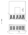
- FIG. 2 shown to be illustrative and not limiting, illustrates a bottom surface of an interposer (left with respect to FIG. 2 ) and a top surface of a printed circuit board (right with respect to FIG. 2 ) in accordance with an embodiment of the present invention.
- Interposer 250 includes ground plane 210 and multiple signal conductors 220.
- Ground plane 210 may be formed on an inner conductive layer within interposer 250.
- the conductive layer with ground plane 220 may be adjacent to a surface layer of interposer 250 that includes signal conductors 220.
- each signal conductor 220 and ground plane 210 collectively form a micro-strip transmission line.
- the micro-strip transmission line may be similar to micro-strip transmission line 151 of FIG. 1 .
- interposer 150 of FIG. 1 may be similar to the bottom surface of interposer 250, in one embodiment.
- interposer 250 includes ten signal conductors 220. Each signal conductor 220 may transmit a single-ended signal. Alternatively, a pair of signal conductors 220 may be utilized to transmit differential signals. As shown in FIG. 2 , the pitch distance between two adjacent signal conductors 220 changes from a relatively small pitch distance (near the center of interposer 250) to a relatively large pitch distance (near the peripheral region of interposer 250).
- signal conductors 220 nearer to the center region of interposer 250 may be coupled to micro-vias in a package substrate (e.g., micro-via 114 of package substrate 110 shown in FIG. 1 ), which may have a small pitch distance, whereas signal conductors 220 nearer to the peripheral region of interposer 250 may be coupled to PCB conductors 131 shown in Fig. 1 , which may have a larger pitch distance.
- printed circuit board 230 includes signal conductors 240 and ground plane 250. As shown in the embodiment of FIG. 2 , signal conductor 240 and ground plane 250 are on printed circuit board 230 whereas signal conductor 220 and ground plane 210 are on interposer 250. Similar to ground plane 210, ground plane 250 may be formed on an inner conductive layer within printed circuit board 230 that is adjacent to a surface layer of printed circuit board 230 that includes signal conductors 240. Each conductor 240 and ground plane 250 form a micro-strip transmission line. In one embodiment, the micro-strip transmission line on the printed circuit board 230 may be similar to micro-strip transmission line 131 of FIG. 1 . The top surface of printed circuit board 130 of FIG.
- top surface of printed circuit board 230 may include ten signal conductors 240.
- Signal conductors 240 may be utilized to transmit either a single-ended signal on each conductor 240 or differential signals on each pair of conductors 240.
- the pitch distance between two adjacent signal conductors 240 may be the same along the signal conductors (unlike signal conductors 220). In general, any desired number of conductive lines 220 and 240 may be used.
- FIG. 3 shown to be illustrative and not limiting, illustrates an integrated circuit package mounted on top of a printed circuit board in accordance with an embodiment of the present invention.
- Integrated circuit package 300 includes integrated circuit die 320, package substrate 310 and interposer 350.
- Printed circuit board 330 includes a cavity where package substrate 310 may be placed or formed.
- integrated circuit package 300, integrated circuit die 320, package substrate 310, interposer 350 and printed circuit board 330 may be similar to integrated circuit package 100, integrated circuit die 120, package substrate 110, interposer 150 and printed circuit board 130 of FIG. 1 , respectively.
- micro solder balls 352 may be utilized to couple interposer 350 to a surface of package substrate 310 and a surface of printed circuit board 330.
- solder balls 352 may be C4 bumps, copper pillars or any conductive joints.
- solder balls 352 may be coupled to the surface of package substrate 310 and the surface of printed circuit board 330 by using a standard solder reflow technique.
- solder balls 352 may have a pitch distance of at least 200 micrometers ( ⁇ m).
- An I/O signal (or other type of data signal) transmitted from integrated circuit die 320 to printed circuit board 330 may propagate through bump 321, bump pad 313, micro-via 312, stripline transmission line 311, micro-via 314, solder pad 315, solder ball 352, micro-strip transmission line 351, solder ball 352 and micro-strip transmission line 331 (in the stated sequence).
- An I/O signal (or other type of data signal) transmitted from printed circuit board 330 to integrated circuit die 320 may propagate through micro-strip transmission line 331, solder ball 352, micro-strip transmission line 351, another solder ball 352, solder pad 315, micro-via 314, stripline transmission line 311, micro-via 312, bump pad 313 and bump 321 (in the stated sequence).
- the embodiment of FIG. 3 may have reduced signal performance relative to the embodiment of FIG. 1 in some scenarios. This is because solder ball 352 is larger than micro-via 314, micro-strip lines 331 and 351 and transmission line 311, and hence may introduce a larger dimensional mismatch to the I/O signal being transmitted. However, this dimensional mismatch is still much smaller than a conventional BGA ball transition, and the structure in embodiment of FIG. 3 may utilize available semiconductor fabrication processes, for example the processes to form solder balls.
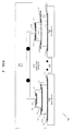
- FIG. 4 shown to be illustrative and not limiting, illustrates an integrated circuit package mounted on top of a multi-tiered printed circuit board in accordance with an embodiment of the present invention.
- Integrated circuit package 400 includes integrated circuit die 420, package substrate 410 and interposer 450.
- Printed circuit board 430 includes a cavity where package substrate 410 may be placed or formed.
- integrated circuit package 400 may be similar to integrated circuit package 100 of FIG. 1 or integrated circuit package 300 of FIG. 3 .
- a multi-tiered package substrate 410 and multi-tiered interposer 450 are used in the structure shown in FIG. 4 . As shown in the embodiment of FIG.
- package substrate 410 and interposer 450 may have three conductive layers.
- the edges of package substrate 410 and interposer 450 may form steps, and therefore may be referred to as step-shaped edges.
- Each edge for the multi-tiered package substrate 410 may include multiple micro-strip transmission lines 411 that are connected to integrated circuit die 420 through signal pathways within the package substrate 410.
- micro-strip transmission lines 411 may be utilized to transmit high speed signals (e.g., signals with data rates greater than 25 Gbps).
- each edge for the multi-tiered interposer 450 may include micro-strip transmission lines 451. High speed data signals transmitting between package substrate 410 and printed circuit board 430 may propagate through micro-strip transmission lines 451.
- the edges of package substrate 410 and interposer 450 may complement each other. Similar to multi-tiered package substrate 410 and interposer 450, printed circuit board 430 may also be formed from three layers. Edges of the cavity within printed circuit board 430 may form steps where interposer 450 may rest. As shown in the embodiment of FIG. 4 , each edge for the printed circuit board 430 may include multiple micro-strip transmission lines 431.
- the embodiment of FIG. 4 may have a signal performance similar to the embodiment of FIG. 1 .
- the embodiment of FIG. 4 may be implemented when a large amount of high speed signal channels are required.
- the structure shown in FIG. 4 may include at least three times more high speed signal channels compared to the embodiment of FIG. 1 .
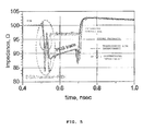
- FIG. 5 shown to be illustrative and not limiting, illustrates signal performances of a differential I/O signal when transmitted through a transmission line interconnect signal pathway(shown by a solid line) and a conventional interconnect signal pathway (shown by a dashed line) in accordance with an embodiment of the present invention.
- the transmission line interconnect signal pathway may be similar to a signal pathway that includes solder ball 121, micro-vias 112 and 114, stripline transmission line 111 and micro-strip transmission lines 131 and 151 of FIG. 1 .
- the conventional interconnect signal pathway may be similar to a signal pathway that includes micro-vias 116 and 118, PTH via 117 and BGA ball 115 but without corresponding transmission line structures.
- the signal performance may be measured by its impedance values at different stages of the signal pathway.
- An impedance of 100 Ohms when transmitting differential signals may indicate a non-reflection loss signal transmission.
- a non-reflection signal transmission may be observed between 0.4 nanoseconds (ns) and 0.5 ns (i.e., when the I/O signal is transmitting through an ideal printed circuit board) for both signal pathways.
- the integrated circuit die e.g., integrated circuit 120 of FIG. 1
- the signal performance for both signal pathways may have impedances valued at 102 Ohms (which is relatively close to 100 Ohms, and therefore may still be determined as non-reflection for an ideal die termination).
- the impedance of the conventional interconnect signal pathway fluctuates more than the impedance of the transmission line interconnect signal pathway.
- the transmission line signal pathway may have a lower parasitic inductance and capacitance(as a result of microwave signal properties of a transmission line structure) and a lower dimensional discontinuity (as shown by I/O signal pathways of the respective embodiments of FIGS. 1 , 3 and 4 ) compared to the conventional interconnect signal pathway.
- programmable logic devices include programmable arrays logic (PALs), programmable logic arrays (PLAs), field programmable logic arrays (FPLAs), electrically programmable logic devices (EPLDs), electrically erasable programmable logic devices (EEPLDs), logic cell arrays (LCAs), complex programmable logic devices (CPLDs), and field programmable gate arrays (FPGAs), just to name a few.
- PALs programmable arrays logic
- PLAs programmable logic arrays
- FPLAs field programmable logic arrays
- EPLDs electrically programmable logic devices
- EEPLDs electrically erasable programmable logic devices
- LCAs logic cell arrays
- CPLDs complex programmable logic devices
- FPGAs field programmable gate arrays
- the programmable logic device described in one or more embodiments herein may be part of a data processing system that includes one or more of the following components: a processor; memory; IO circuitry; and peripheral devices.
- the data processing can be used in a wide variety of applications, such as computer networking, data networking, instrumentation, video processing, digital signal processing, or any suitable other applications where the advantage of using programmable or re-programmable logic is desirable.
- the programmable logic device can be used to perform a variety of different logic functions.
- the programmable logic device can be configured as a processor or controller that works in cooperation with a system processor.
- the programmable logic device may also be used as an arbiter for arbitrating access to a shared resource in the data processing system.
- the programmable logic device can be configured as an interface between a processor and one of the other components in the system.
- the programmable logic device may be one of the family of devices owned by ALTERA Corporation.
Landscapes
- Engineering & Computer Science (AREA)
- Microelectronics & Electronic Packaging (AREA)
- Structure Of Printed Boards (AREA)
- Chemical & Material Sciences (AREA)
- Materials Engineering (AREA)
- Production Of Multi-Layered Print Wiring Board (AREA)
- Physics & Mathematics (AREA)
- Geometry (AREA)
- Structures For Mounting Electric Components On Printed Circuit Boards (AREA)
Abstract
Description
- Generally, a circuit system has multiple integrated circuit packages placed on a printed circuit board (PCB). Each integrated circuit package is coupled to the printed circuit board using a particular type of interconnect structure. Commonly known interconnect structures at the package/PCB interface include ball grid arrays (BGAs), land grid arrays (LGAs), pin grid arrays (PGAs) and surface mounted technology (SMT) pins.
- However, these interconnect structures may not be able to support a high-speed circuit system (e.g., a circuit system with a data transfer rate that is greater than 25 gigabits per second (Gbps)). Such a limitation may be due to: (i) dimension mismatches between structures utilized to transmit signals within a package substrate and at the package/PCB interface, and (ii) parasitic inductances of the interconnect structures.
- In most interconnect structures, the largest dimension mismatch is observed between a micro-via, a plated through-hole (PTH) via, and a BGA ball. Parasitic inductance may be an intrinsic characteristic of a pin that forms part of the interconnect structure. The parasitic inductance causes an inductive impedance mismatch for a transmitted signal. Hence, the two limitations can reduce the bandwidth of the interconnect structures and can increase unwanted higher-order mode signal problems in a high-speed circuit system.
- The above-mentioned problems are sometimes resolved using micro-wave interconnect technology. However, micro-wave interconnect technology generally involves a large diameter (i.e., 3 millimeter (mm)) as a result of similar designs to a coaxial pin structure. This significantly reduces channel density between an integrated circuit package and a printed circuit board.
- Embodiments described herein include transmission line bridge interconnects. It should be appreciated that the embodiments can be implemented in numerous ways, such as a process, an apparatus, a system, a device, or a method. Several embodiments are described below.
- In one embodiment, an integrated circuit package includes a package substrate, an interposer structure, a printed circuit board and a transmission line. The interposer structure, which includes multiple interposer layers, may be formed at a top surface of the package substrate. The printed circuit board may be coupled to the package substrate. The transmission line may be formed on at least one of the interposer layers. The transmission line may be utilized to convey signals between the package substrate and the printed circuit board. In one embodiment, the transmission line may be a stripline transmission line or a micro-strip transmission line. The transmission line may have a low parasitic inductance and implementation of the transmission line does not introduce large dimensional discontinuity throughout a signal pathway. The integrated circuit package may be part of a circuit system that includes external circuits.
- Further features of the invention, its nature and various advantages will be more apparent from the accompanying drawings and the following detailed description of the preferred embodiments.
-
-
FIG. 1 shows an illustrative transmission line bridge interconnect that couples an integrated circuit package to a printed circuit board in accordance with an embodiment of the present invention. -
FIG. 2 shows an illustrative bottom surface of an interposer (left) and a top surface of a printed circuit board (right) in accordance with an embodiment of the present invention. -
FIG. 3 shows an illustrative integrated circuit package coupled to a printed circuit board through a micro solder joint bridge interconnect in accordance with an embodiment of the present invention. -
FIG. 4 shows an illustrative integrated circuit package coupled to a printed circuit board using multi-tiered bridge interconnect in accordance with an embodiment of the present invention. -
FIG. 5 shows how signal performances when a differential I/O signal is transmitted through a transmission line interconnect signal pathway may be optimized in accordance with an embodiment of the present invention. - The following embodiments describe an integrated circuit package with transmission line bridge interconnects. It will be obvious, to one skilled in the art, that the present exemplary embodiments may be practiced without some or all of these specific details. In other instances, well-known operations have not been described in detail in order not to unnecessarily obscure the present embodiments.
-
FIG. 1 , meant to be illustrative and not limiting, illustrates a transmission line bridge interconnect that couples an integrated circuit package to a printed circuit board in accordance with one embodiment of the present invention.Integrated circuit package 100 includes integrated circuit die 120,package substrate 110,heat sink 140 andinterposer 150. Printedcircuit board 130 includes a cavity, in whichpackage substrate 110 may be placed or formed. -
Integrated circuit package 100 may be an application specific integrated circuit (ASIC) device or an application specific standard product (ASSP) device, in one embodiment. An ASIC or ASSP device has fixed functions and therefore, the ASIC or ASSP device may have specialized circuitry to perform the fixed functions. In one embodiment, the ASIC or ASSP device may be a memory controller device. Alternatively,integrated circuit package 100 may be a programmable logic device (PLD), such as a field programmable gate array (FPGA) device. An FPGA device may be programmed to perform different functions. Therefore, the FPGA device may include multiple of programmable logic elements to enable itself to be programmed to perform the various functions. - Integrated circuit die 120 may be a semiconductor die (e.g., a silicon die). Generally, integrated circuit die 120 performs the core functions of
integrated circuit package 100. Integrated circuit die 120 may include multiple circuit structures, for example, complementary metal oxide semiconductor (CMOS) transistors, capacitors and inductor structures. The circuit structures may form functional circuitry that performs functions defined forintegrated circuit die 120. For example, integrated circuit die 120 may have multiple functional circuitry (e.g., transceiver circuitry) that transfers data from an ASIC or ASSP device (e.g., a memory controller device) to a memory device (i.e., an external device). The transceiver circuitry may be capable of transmitting a signal (i.e., TX signal) or may receive a signal (i.e., a RX signal). Alternatively, integrated circuit die 120 may have multiple programmable logic elements and programmable interconnects within an FPGA device that perform various functions based on user requirements. - Referring still to
FIG. 1 , integrated circuit die 120 is mounted on a top surface ofpackage substrate 110. Integrated circuit die 120 may be coupled topackage substrate 110 through bumps 121 (e.g., in a flip chip assembly). In one embodiment,bumps 121 may be controlled collapse chip connection (C4) bumps. Eachbump 121 may be coupled to its corresponding transceiver circuitry (not shown) within the integrated circuit die 120, in one embodiment. As shown in the embodiment ofFIG. 1 , for everybump 121 onintegrated circuit die 120, there may be acorresponding bump pad 113 onpackage substrate 110. Input/output (I/O) signals may be transmitted betweenintegrated circuit die 120 andpackage substrate 110 through at least some of thebumps 121 andbump pads 113. In one embodiment, the I/O signals may be high-speed signals, which carry information at a high data rate such as 25 gigabits per second (Gbps) or higher. Alternatively, radio-frequency data signals may be transmitted through a portion ofbumps 121 andbump pads 113. Theremaining bumps 121 andbump pads 113 may be utilized to provide power and ground voltage signals to integratedcircuit die 120. - As shown in
FIG. 1 ,heat sink 140 may be coupled to the back side of theintegrated circuit die 120.Heat sink 140 may maintain an optimum operating temperature for integrated circuit die 120. It should be appreciated thatheat sink 140 may help to dissipate excess heat generated by integratedcircuit die 120 during operation. It should be noted that the optimum operating temperature for an integrated circuit die (e.g., integrated circuit die 120) may vary according to the function of theintegrated circuit die 120 and the extent of its operation. - As shown in the embodiment of
FIG. 1 ,package substrate 110 may be coupled to a top surface of integrated circuit die 120 using a flip chip technology.Package substrate 110 may includebump pads 113, micro-vias (µ-vias) 112, 114, 116 and 118, plated through-hole (PTH) via 117 andtransmission line 111. Any of thebump pads 113 may be coupled to asolder ball 115 through a series ofmicro-vias 116, PTH via 117 and a series ofmicro-vias 118. In the embodiment ofFIG. 1 ,solder balls 115 may be ball grid array (BGA) balls. Alternatively,package substrate 110 implementing a land grid array (LGA) technology, a pin grid array (PGA) technology or a surface mounted technology (SMT) may include corresponding pin structures (not shown) instead ofsolder balls 115.Solder balls 115 may be directly coupled to printedcircuit board 130. In one embodiment, low speed I/O signals, power and/or ground voltage signals provided by an external source (e.g., a power source on or coupled to printed circuit board 130) may be transmitted to integrated circuit die 120 through a pathway that includesbump pad 113, micro-vias 116 and 118, PTH via 117 andBGA ball 115. - Bump
pads 113 that are not coupled to the power source may be coupled tomicro-via 112. As shown in the embodiment ofFIG. 1 , micro-via 112 forms a part of a signal pathway that includestransmission line 111 andmicro-via 114.Micro-via 112 may be coupled to one end oftransmission line 111 whereasmicro-via 114 is coupled to the other end oftransmission line 111. It should be appreciated thatmicro-via bump pad 113, micro-vias 112 and 114 andtransmission line 111 may be utilized for transmitting high speed I/O signals between an external circuit (i.e., external to integrated circuit package 100) and an integrated circuit die 120. It should be appreciated that there may be multiple pathways similar to the one shown in the embodiment ofFIG. 1 . In one embodiment, the number of pathways may correspond to the number ofbumps 121 that may be utilized for transmitting high speed I/O signals (such as, RX signals and TX signals) for integrated circuit die 120. - In one embodiment,
transmission line 111 may be a stripline transmission line. It should be appreciated that the stripline transmission line may include a signal conductor that is sandwiched between two parallel ground planes (one above the signal conductor and one below the signal conductor, whereby the ground planes are not shown inFIG. 1 ). The signal conductor and the ground planes fortransmission line 111 may be formed using copper, for example.Transmission line 111 may be utilized to transmit high-speed signals (e.g., signals having data rates greater than 25 Gbps). In one embodiment,transmission line 111 may exhibit a characteristic impedance of 50 Ohms when it is designed to transmit single-ended signals. Alternatively,transmission line 111 may exhibit a characteristic impedance of 100 Ohms when it is designed to transmit differential signals. In general,line 111 may have any desired impedance.Transmission line 111 may have a relatively small (or, in some instances, non-existent) parasitic inductance. Therefore, the parasitic inductance may be negligible fortransmission line 111 and may be disregarded in order to determine signal behavior acrosstransmission line 111. - Referring still to
FIG. 1 ,interposer 150 is formed partially on top ofpackage substrate 110 and partially on top of printedcircuit board 130. In one embodiment,interposer 150 may be formed as a single structure.Interposer 150 may be formed such thatinterposer 150 surrounds integrated circuit die 120. A top surface ofinterposer 150 may also be coupled toheat sink 140. -
Interposer 150 may include at least onemicro-strip transmission line 151. As shown in the embodiment ofFIG. 1 ,micro-strip transmission line 151 is coupled to micro-via 114 inintegrated package substrate 110. In one embodiment,micro-strip transmission line 151 may be known as a `bridge' connection betweenpackage substrate 110 and an external circuit (e.g., printed circuit board 130). The I/O signals that are transmitted through the signal pathway (that includesbump pad 113, micro-vias 112 and 114 and transmission line 111) may then propagate throughmicro-strip transmission line 151 to external circuits.Micro-strip transmission line 151 may have a characteristic impedance of either 50 Ohms or 100 Ohms depending on whethermicro-strip transmission line 151 is designed to transmit single-ended signals or differential signals. In general,line 151 may have any desired impedance. In one embodiment,micro-strip transmission line 151 may follow the characteristic impedance oftransmission line 111. It should be appreciated thatmicro-strip transmission line 151 may include a signal conductor that transmits the signals (as shown in the embodiment ofFIG. 1 ) and a ground plane (that is not shown for the sake of clarity). The ground plane may be formed in a conductive layer withininterposer 150 that is directly adjacent to a conductive layer that includes the signal conductor. - Alternatively,
interposer 150 may include a stripline transmission line (not shown).Interposer 150 with the stripline transmission line may include a signal conductor within an inner conductive layer of interposer 150 (rather than a signal conductor formed on a surface layer ofinterposer 150 for micro-strip transmission line 151). Similar to micro-striptransmission line 151, the stripline transmission line may also have a characteristic impedance of 50 Ohms (when designed to transmit single-ended signals) or 100 Ohms (when designed to transmit differential signals). Similar totransmission line 111, the signal conductor and the ground plane forming micro-strip transmission line 151 (or a stripline transmission line) may be formed from copper. - As shown in the embodiment of
FIG. 1 , a portion ofmicro-strip transmission line 151 may be coupled tomicro-strip transmission line 131.Micro-strip transmission line 131 may be formed on a surface of printedcircuit board 130.Micro-strip transmission line 131 may have a characteristic impedance that is similar to that ofmicro-strip transmission line 151 andtransmission line 111. In one embodiment,micro-strip transmission line 131 may have a characteristic impedance of 50 Ohms (whenmicro-strip transmission line 131 is designed to transmit single-ended signals) or 100 Ohms (whenmicro-strip transmission line 131 is designed to transmit differential signals). In general,line 131 may have any desired impedance. - Printed
circuit board 130 may include a cavity. As shown in the embodiment ofFIG. 1 ,package substrate 110 may be placed or formed within the cavity. The cavity may be sufficiently large to accommodate theentire package substrate 110. It should be appreciated that printedcircuit board 130 may also include other integrated circuit packages (not shown inFIG. 1 ) that are mounted on top of its surface. For example, there may be multiples devices, such as, a memory device and a microprocessor device formed on printedcircuit board 130. These devices may be part of the external circuitry coupled to integratedcircuit package 100. - In one embodiment,
interposer 150 may be coupled topackage substrate 110 and printedcircuit board 130 through a copper-to-copper bonding process. The copper-to-copper bonding process may bond the copper materials withinmicro-strip transmission lines micro-strip transmission line 151 andmicro-via 114. In addition,interposer 150 may be fixed to its location using a pin or a bolt. The pin/bolt may protrude from printedcircuit board 130 and prevent interposer 150 from moving freely. - The embodiment in
FIG. 1 usesmicro-strip transmission line 151 to coupleintegrated circuit package 100 and printedcircuit board 130. Themicro-strip transmission line 151 may have a tapered shape so that its line width at the PCB end is the same asmicro-strip transmission line 131, and therefore there is a smooth dimensional transition between the structures that transmit signals. If desired,micro-strip line 151 may also have little or no parasitic inductance. - It should be appreciated that transmission lines (e.g.,
micro-strip transmission lines -
FIG. 2 , meant to be illustrative and not limiting, illustrates a bottom surface of an interposer (left with respect toFIG. 2 ) and a top surface of a printed circuit board (right with respect toFIG. 2 ) in accordance with an embodiment of the present invention.Interposer 250 includesground plane 210 andmultiple signal conductors 220.Ground plane 210 may be formed on an inner conductive layer withininterposer 250. The conductive layer withground plane 220 may be adjacent to a surface layer ofinterposer 250 that includessignal conductors 220. In one embodiment, eachsignal conductor 220 andground plane 210 collectively form a micro-strip transmission line. The micro-strip transmission line may be similar tomicro-strip transmission line 151 ofFIG. 1 . The bottom surface ofinterposer 150 ofFIG. 1 may be similar to the bottom surface ofinterposer 250, in one embodiment. In the embodiment ofFIG. 2 ,interposer 250 includes tensignal conductors 220. Eachsignal conductor 220 may transmit a single-ended signal. Alternatively, a pair ofsignal conductors 220 may be utilized to transmit differential signals. As shown inFIG. 2 , the pitch distance between twoadjacent signal conductors 220 changes from a relatively small pitch distance (near the center of interposer 250) to a relatively large pitch distance (near the peripheral region of interposer 250). This is becausesignal conductors 220 nearer to the center region ofinterposer 250 may be coupled to micro-vias in a package substrate (e.g., micro-via 114 ofpackage substrate 110 shown inFIG. 1 ), which may have a small pitch distance, whereassignal conductors 220 nearer to the peripheral region ofinterposer 250 may be coupled toPCB conductors 131 shown inFig. 1 , which may have a larger pitch distance. - Referring still to
FIG. 2 , printed circuit board 230 includessignal conductors 240 andground plane 250. As shown in the embodiment ofFIG. 2 ,signal conductor 240 andground plane 250 are on printed circuit board 230 whereassignal conductor 220 andground plane 210 are oninterposer 250. Similar toground plane 210,ground plane 250 may be formed on an inner conductive layer within printed circuit board 230 that is adjacent to a surface layer of printed circuit board 230 that includessignal conductors 240. Eachconductor 240 andground plane 250 form a micro-strip transmission line. In one embodiment, the micro-strip transmission line on the printed circuit board 230 may be similar tomicro-strip transmission line 131 ofFIG. 1 . The top surface of printedcircuit board 130 ofFIG. 1 may be similar to the top surface of printed circuit board 230, in one embodiment. In one embodiment, top surface of printed circuit board 230 may include tensignal conductors 240.Signal conductors 240 may be utilized to transmit either a single-ended signal on eachconductor 240 or differential signals on each pair ofconductors 240. As shown in the embodiment ofFIG. 2 , the pitch distance between twoadjacent signal conductors 240 may be the same along the signal conductors (unlike signal conductors 220). In general, any desired number ofconductive lines -
FIG. 3 , meant to be illustrative and not limiting, illustrates an integrated circuit package mounted on top of a printed circuit board in accordance with an embodiment of the present invention. Integratedcircuit package 300 includes integrated circuit die 320,package substrate 310 andinterposer 350. Printedcircuit board 330 includes a cavity wherepackage substrate 310 may be placed or formed. In one embodiment, integratedcircuit package 300, integrated circuit die 320,package substrate 310,interposer 350 and printedcircuit board 330 may be similar tointegrated circuit package 100, integrated circuit die 120,package substrate 110,interposer 150 and printedcircuit board 130 ofFIG. 1 , respectively. Therefore, for the sake of brevity, the details ofintegrated circuit package 300, integrated circuit die 320,package substrate 310,interposer 350 and printedcircuit board 330 are not repeated. Unlike the embodiment ofFIG. 1 ,micro solder balls 352 may be utilized to couple interposer 350 to a surface ofpackage substrate 310 and a surface of printedcircuit board 330. In one embodiment,solder balls 352 may be C4 bumps, copper pillars or any conductive joints. In one embodiment,solder balls 352 may be coupled to the surface ofpackage substrate 310 and the surface of printedcircuit board 330 by using a standard solder reflow technique. In one embodiment,solder balls 352 may have a pitch distance of at least 200 micrometers (µm). - An I/O signal (or other type of data signal) transmitted from integrated circuit die 320 to printed
circuit board 330 may propagate throughbump 321,bump pad 313, micro-via 312,stripline transmission line 311, micro-via 314,solder pad 315,solder ball 352,micro-strip transmission line 351,solder ball 352 and micro-strip transmission line 331 (in the stated sequence). An I/O signal (or other type of data signal) transmitted from printedcircuit board 330 to integrated circuit die 320 may propagate throughmicro-strip transmission line 331,solder ball 352,micro-strip transmission line 351, anothersolder ball 352,solder pad 315, micro-via 314,stripline transmission line 311, micro-via 312,bump pad 313 and bump 321 (in the stated sequence). - It should be appreciated that the embodiment of
FIG. 3 may have reduced signal performance relative to the embodiment ofFIG. 1 in some scenarios. This is becausesolder ball 352 is larger thanmicro-via 314,micro-strip lines transmission line 311, and hence may introduce a larger dimensional mismatch to the I/O signal being transmitted. However, this dimensional mismatch is still much smaller than a conventional BGA ball transition, and the structure in embodiment ofFIG. 3 may utilize available semiconductor fabrication processes, for example the processes to form solder balls. -
FIG. 4 , meant to be illustrative and not limiting, illustrates an integrated circuit package mounted on top of a multi-tiered printed circuit board in accordance with an embodiment of the present invention. Integratedcircuit package 400 includes integrated circuit die 420,package substrate 410 andinterposer 450. Printedcircuit board 430 includes a cavity wherepackage substrate 410 may be placed or formed. In one embodiment, integratedcircuit package 400 may be similar tointegrated circuit package 100 ofFIG. 1 or integratedcircuit package 300 ofFIG. 3 . However, unlike the embodiments shown inFIGS. 1 and3 , amulti-tiered package substrate 410 andmulti-tiered interposer 450 are used in the structure shown inFIG. 4 . As shown in the embodiment ofFIG. 4 ,package substrate 410 andinterposer 450 may have three conductive layers. The edges ofpackage substrate 410 andinterposer 450 may form steps, and therefore may be referred to as step-shaped edges. Each edge for themulti-tiered package substrate 410 may include multiplemicro-strip transmission lines 411 that are connected to integrated circuit die 420 through signal pathways within thepackage substrate 410. In one embodiment,micro-strip transmission lines 411 may be utilized to transmit high speed signals (e.g., signals with data rates greater than 25 Gbps). Similarly, each edge for themulti-tiered interposer 450 may includemicro-strip transmission lines 451. High speed data signals transmitting betweenpackage substrate 410 and printedcircuit board 430 may propagate throughmicro-strip transmission lines 451. As shown in the embodiment ofFIG. 4 , the edges ofpackage substrate 410 andinterposer 450 may complement each other. Similar tomulti-tiered package substrate 410 andinterposer 450, printedcircuit board 430 may also be formed from three layers. Edges of the cavity within printedcircuit board 430 may form steps whereinterposer 450 may rest. As shown in the embodiment ofFIG. 4 , each edge for the printedcircuit board 430 may include multiplemicro-strip transmission lines 431. - The embodiment of
FIG. 4 may have a signal performance similar to the embodiment ofFIG. 1 . In addition, the embodiment ofFIG. 4 may be implemented when a large amount of high speed signal channels are required. In one embodiment, the structure shown inFIG. 4 may include at least three times more high speed signal channels compared to the embodiment ofFIG. 1 . -
FIG. 5 , meant to be illustrative and not limiting, illustrates signal performances of a differential I/O signal when transmitted through a transmission line interconnect signal pathway(shown by a solid line) and a conventional interconnect signal pathway (shown by a dashed line) in accordance with an embodiment of the present invention. In one embodiment, the transmission line interconnect signal pathway may be similar to a signal pathway that includessolder ball 121, micro-vias 112 and 114,stripline transmission line 111 andmicro-strip transmission lines FIG. 1 . The conventional interconnect signal pathway may be similar to a signal pathway that includes micro-vias 116 and 118, PTH via 117 andBGA ball 115 but without corresponding transmission line structures. - Referring still to
FIG. 5 , the signal performance may be measured by its impedance values at different stages of the signal pathway. An impedance of 100 Ohms when transmitting differential signals may indicate a non-reflection loss signal transmission. InFIG. 5 , a non-reflection signal transmission may be observed between 0.4 nanoseconds (ns) and 0.5 ns (i.e., when the I/O signal is transmitting through an ideal printed circuit board) for both signal pathways. Once the differential signals reach the integrated circuit die (e.g., integratedcircuit 120 ofFIG. 1 ) the signal performance for both signal pathways may have impedances valued at 102 Ohms (which is relatively close to 100 Ohms, and therefore may still be determined as non-reflection for an ideal die termination). - However, signal performances for the conventional signal pathway and the transmission line interconnect signal pathway differ significantly between 0.5 ns to 0.6 ns (i.e., when the differential signals are transmitted through a package substrate and an interposer). As shown in the embodiment of
FIG. 5 , the impedance of the conventional interconnect signal pathway fluctuates more than the impedance of the transmission line interconnect signal pathway. This is because the transmission line signal pathway may have a lower parasitic inductance and capacitance(as a result of microwave signal properties of a transmission line structure) and a lower dimensional discontinuity (as shown by I/O signal pathways of the respective embodiments ofFIGS. 1 ,3 and4 ) compared to the conventional interconnect signal pathway. - The embodiments thus far have been described with respect to integrated circuits. The methods and apparatuses described herein may be incorporated into any suitable circuits. For example, they may be incorporated into numerous types of devices such as programmable logic devices, application specific standard products (ASSPs), and application specific integrated circuits (ASICs). Examples of programmable logic devices include programmable arrays logic (PALs), programmable logic arrays (PLAs), field programmable logic arrays (FPLAs), electrically programmable logic devices (EPLDs), electrically erasable programmable logic devices (EEPLDs), logic cell arrays (LCAs), complex programmable logic devices (CPLDs), and field programmable gate arrays (FPGAs), just to name a few.
- The programmable logic device described in one or more embodiments herein may be part of a data processing system that includes one or more of the following components: a processor; memory; IO circuitry; and peripheral devices. The data processing can be used in a wide variety of applications, such as computer networking, data networking, instrumentation, video processing, digital signal processing, or any suitable other applications where the advantage of using programmable or re-programmable logic is desirable. The programmable logic device can be used to perform a variety of different logic functions. For example, the programmable logic device can be configured as a processor or controller that works in cooperation with a system processor. The programmable logic device may also be used as an arbiter for arbitrating access to a shared resource in the data processing system. In yet another example, the programmable logic device can be configured as an interface between a processor and one of the other components in the system. In one embodiment, the programmable logic device may be one of the family of devices owned by ALTERA Corporation.
- Although the methods of operations were described in a specific order, it should be understood that other operations may be performed in between described operations, described operations may be adjusted so that they occur at slightly different times or described operations may be distributed in a system which allows occurrence of the processing operations at various intervals associated with the processing, as long as the processing of the overlay operations are performed in a desired way.
- Although the foregoing invention has been described in some detail for the purposes of clarity, it will be apparent that certain changes and modifications can be practiced by a person skilled in the art.. Accordingly, the present embodiments are to be considered as illustrative and not restrictive, and the invention is not to be limited to the details given herein.
-
- Additional embodiment 1. An integrated circuit package, comprising: a package substrate; an interposer structure formed at a top surface of the package substrate, wherein the interposer structure comprises a plurality of interposer layers; and a transmission line formed on at least one of the plurality of interposer layers, wherein the transmission line conveys signals between the package substrate and an external circuit.
- Additional embodiment 2. The integrated circuit package of additional embodiment 1, wherein the transmission line comprises a transmission line selected from the group consisting of: a micro-strip transmission line and a stripline transmission line.
- Additional embodiment 3. The integrated circuit package of additional embodiment 1, further comprising: an additional transmission line formed on the at least one of the plurality of interposer layers, wherein the transmission line transmits a first signal from the package substrate to a printed circuit board and wherein the additional transmission line transmits a second signal from the printed circuit board to the package substrate.
- Additional embodiment 4. The integrated circuit package of additional embodiment 3, wherein the first signal transmitted from the package substrate comprises a signal selected from the group consisting of: a single-ended signal and a differential signal.
- Additional embodiment 5. The integrated circuit package of additional embodiment 1, wherein a characteristic impedance of the transmission line is at least 50 Ohm.
- Additional embodiment 6. The integrated circuit package of additional embodiment 1, wherein the interposer structure has an edge with a plurality of steps, wherein a respective transmission line is formed on each of the steps of the plurality of steps.
- Additional embodiment 7. The integrated circuit package of additional embodiment 1, wherein the signals comprise signals selected from the group consisting of: input-output signals, radio-frequency data signals, power signals, and ground signals.
- Additional embodiment 8. The integrated circuit package of additional embodiment 1, further comprising: an integrated circuit die formed on the package substrate, wherein the interposer structure surrounds the integrated circuit die.
- Additional embodiment 9. A system, comprising:
- an integrated circuit die; a substrate, wherein the integrated circuit die is mounted on a top surface of the substrate; an interposer formed above the substrate that at least partially surrounds the integrated circuit die; and
- a transmission line formed within the interposer, wherein the transmission line transmits a signal between the integrated circuit die and an external circuit.
- Additional embodiment 10. The system of additional embodiment 9, further comprising: a printed circuit board, wherein the printed circuit board comprises a cavity and wherein the substrate is formed within the cavity.
- Additional embodiment 11. The system of additional embodiment 10, wherein the printed circuit board further comprises: an additional transmission line at a surface of the printed circuit board that faces the interposer, wherein the transmission line on the interposer partially overlaps the additional transmission line on the printed circuit board so that the signal is transmitted between the additional transmission line on the printed circuit board and the transmission line on the interposer.
- Additional embodiment 12. The system of additional embodiment, wherein the transmission line comprises a transmission line selected from the group consisting of: a micro-strip transmission line and a stripline transmission line.
- Additional embodiment 13. The system of additional embodiment 9, further comprising: an additional transmission line formed within the interposer, wherein the transmission line transmits an additional signal between the integrated circuit die and the external circuit, wherein the transmission line is formed in a first plane within the interposer and the additional transmission line is formed in a third plane that is different from the first plane within the interposer.
- Additional embodiment 14. The system of additional embodiment 9, wherein the signal transmitted by the transmission line comprises a signal selected from the group consisting of: a single-ended signal and a differential signal.
- Additional embodiment 15. The system of additional embodiment 9, wherein edges of the substrate and edges of the interposer each comprise a plurality of step-shaped structures, wherein each of the step-shaped structures includes at least one corresponding transmission line.
- Additional embodiment 16. An apparatus, comprising: a printed circuit board having a cavity; a package substrate formed within the cavity of the printed circuit board; an interposer having a first portion formed over a top surface of the package substrate and a second portion formed over a top surface of the printed circuit board; and a conductive line formed at the top surface of the printed circuit board that conveys signals between the package substrate and the printed circuit board.
- Additional embodiment 17. The apparatus of additional embodiment 16, further comprising: an integrated circuit die mounted to the top surface of the package substrate, wherein the conductive line formed at the top surface of the printed circuit board conveys the signals between the integrated circuit die and the printed circuit board.
- Additional embodiment 18. The apparatus of additional embodiment 17, further comprising: an additional conductive line formed at a bottom surface of the interposer, wherein the bottom surface of the interposer is formed adjacent to the top surface of the printed circuit board and the top surface of the package substrate, and wherein the conductive line and the additional conductive line convey the signals between the integrated circuit die and the printed circuit board.
- Additional embodiment 19. The apparatus of additional embodiment 18, wherein the conductive line comprises a first radio-frequency transmission line and the additional conductive line comprises a second radio-frequency transmission line.
- Additional embodiment 20. The apparatus of additional embodiment 18, wherein a first end of the additional conductive line is electrically coupled to a first conductive pad on the top surface of the package substrate and a second end of the additional conductive line is coupled to a second conductive pad on the top surface of the printed circuit board.
- Additional embodiment 21. The apparatus of additional embodiment 17, wherein the integrated circuit die transmits signals to the printed circuit board over the conductive line at a data rate greater than 25 gigabits per second.
- Additional embodiment 22. The apparatus of additional embodiment 16, further comprising: an additional conductive line formed adjacent to the conductive line formed at the top surface of the printed circuit board, wherein the conductive line and the additional conductive line comprise transmission lines that transmit differential signals.
Claims (15)
- An integrated circuit package, comprising:a package substrate;an interposer structure formed at a top surface of the package substrate, wherein the interposer structure comprises a plurality of interposer layers; anda transmission line formed on at least one of the plurality of interposer layers, wherein the transmission line conveys signals between the package substrate and an external circuit.
- The integrated circuit package defined in claim 1, wherein the transmission line comprises a transmission line selected from the group consisting of:a micro-strip transmission line and a stripline transmission line.
- The integrated circuit package defined in claim 1 or 2, further comprising:an additional transmission line formed on the at least one of the plurality of interposer layers, wherein the transmission line transmits a first signal from the package substrate to a printed circuit board, wherein the additional transmission line transmits a second signal from the printed circuit board to the package substrate, and wherein the first signal transmitted from the package substrate comprises a signal selected from the group consisting of:a single-ended signal and a differential signal.
- The integrated circuit package defined in one of claims 1 to 3, wherein a characteristic impedance of the transmission line is at least 50 Ohm.
- The integrated circuit package defined in one of claims 1 to 4, wherein the interposer structure has an edge with a plurality of steps, wherein a respective transmission line is formed on each of the steps of the plurality of steps.
- The integrated circuit package defined in one of claims 1 to 5, wherein the signals comprise signals selected from the group consisting of:input-output signals, radio-frequency data signals, power signals, and ground signals.
- The integrated circuit package defined in one of claims 1 to 6, further comprising:an integrated circuit die formed on the package substrate, wherein the interposer structure surrounds the integrated circuit die.
- The integrated circuit defined in claim 7, wherein the transmission line transmits the signals between the integrated circuit die and the external circuit.
- The integrated circuit package defined in claim 8, further comprising:an additional transmission line formed within the interposer structure, wherein the additional transmission line transmits additional signals between the integrated circuit die and the external circuit, wherein the transmission line is formed in a first plane within the interposer structure and the additional transmission line is formed in a second plane that is different from the first plane within the interposer structure.
- The integrated circuit package defined in one of claims 1 to 9, wherein edges of the package substrate and edges of the interposer structure each comprise a plurality of step-shaped structures, wherein each of the step-shaped structures includes at least one corresponding transmission line.
- The integrated circuit package defined in one of claims 1 to 10, further comprising:a printed circuit board having a cavity, wherein the package substrate is formed within the cavity of the printed circuit board, and wherein the interposer has a first portion formed over the top surface of the package substrate and a second portion formed over a top surface of the printed circuit board; anda conductive line formed at the top surface of the printed circuit board that conveys the signals between the package substrate and the external circuit.
- The integrated circuit package defined in claim 11, wherein the transmission line is formed at a bottom surface of the interposer structure, wherein the bottom surface of the interposer structure is formed adjacent to the top surface of the printed circuit board and the top surface of the package substrate, and wherein the conductive line and the transmission line convey the signals between an integrated circuit die and the external circuit.
- The integrated circuit package defined in claim 12, wherein a first end of the transmission line is electrically coupled to a first conductive pad on the top surface of the package substrate and a second end of the transmission line is coupled to a second conductive pad on the top surface of the printed circuit board.
- The integrated circuit package defined in claim 12 or 13, wherein the integrated circuit die transmits signals to the printed circuit board over the conductive line and the transmission line at a data rate greater than 25 gigabits per second.
- The apparatus defined in one of claims 11 to 14, wherein the conductive line and the transmission line both transmit differential signals.
Applications Claiming Priority (1)
| Application Number | Priority Date | Filing Date | Title |
|---|---|---|---|
| US14/860,565 US9842813B2 (en) | 2015-09-21 | 2015-09-21 | Tranmission line bridge interconnects |
Publications (3)
| Publication Number | Publication Date |
|---|---|
| EP3144967A2 true EP3144967A2 (en) | 2017-03-22 |
| EP3144967A3 EP3144967A3 (en) | 2017-05-10 |
| EP3144967B1 EP3144967B1 (en) | 2018-11-21 |
Family
ID=57113032
Family Applications (1)
| Application Number | Title | Priority Date | Filing Date |
|---|---|---|---|
| EP16189120.5A Active EP3144967B1 (en) | 2015-09-21 | 2016-09-16 | Integrated circuit package including an interposer carrying a transmission line |
Country Status (3)
| Country | Link |
|---|---|
| US (1) | US9842813B2 (en) |
| EP (1) | EP3144967B1 (en) |
| CN (1) | CN106549002B (en) |
Cited By (2)
| Publication number | Priority date | Publication date | Assignee | Title |
|---|---|---|---|---|
| WO2020050930A1 (en) * | 2018-09-04 | 2020-03-12 | Raytheon Company | Printed circuit board based rf circuit module |
| CN111741601A (en) * | 2020-07-09 | 2020-10-02 | 复旦大学 | A Universal Configurable Active Substrate Circuit Structure |
Families Citing this family (18)
| Publication number | Priority date | Publication date | Assignee | Title |
|---|---|---|---|---|
| US9713258B2 (en) * | 2006-04-27 | 2017-07-18 | International Business Machines Corporation | Integrated circuit chip packaging |
| US10026720B2 (en) * | 2015-05-20 | 2018-07-17 | Broadpak Corporation | Semiconductor structure and a method of making thereof |
| WO2018236336A1 (en) | 2017-06-19 | 2018-12-27 | Intel Corporation | In-package rf waveguides as high bandwidth chip-to-chip interconnects and methods for using the same |
| DE112017008336T5 (en) | 2017-12-29 | 2020-09-17 | Intel Corporation | Microelectronic assemblies |
| DE112017008326T5 (en) | 2017-12-29 | 2020-10-08 | Intel Corporation | Microelectronic assemblies |
| US11494682B2 (en) | 2017-12-29 | 2022-11-08 | Intel Corporation | Quantum computing assemblies |
| WO2019132967A1 (en) * | 2017-12-29 | 2019-07-04 | Intel Corporation | Microelectronic assemblies |
| US11348897B2 (en) | 2017-12-29 | 2022-05-31 | Intel Corporation | Microelectronic assemblies |
| DE102018102144A1 (en) * | 2018-01-31 | 2019-08-01 | Tdk Electronics Ag | Electronic component |
| US11735570B2 (en) * | 2018-04-04 | 2023-08-22 | Intel Corporation | Fan out packaging pop mechanical attach method |
| US11469206B2 (en) | 2018-06-14 | 2022-10-11 | Intel Corporation | Microelectronic assemblies |
| CN112889149B (en) * | 2019-01-18 | 2023-09-08 | 华为技术有限公司 | Integrated circuit with multiple intermediate layers interconnected |
| US11948855B1 (en) | 2019-09-27 | 2024-04-02 | Rockwell Collins, Inc. | Integrated circuit (IC) package with cantilever multi-chip module (MCM) heat spreader |
| US10917968B1 (en) * | 2019-12-18 | 2021-02-09 | Google Llc | Package to printed circuit board transition |
| CN111599802B (en) * | 2020-05-13 | 2021-12-24 | 中国电子科技集团公司第十三研究所 | Ceramic package shell and package shell mounting structure |
| DE102020128143B4 (en) | 2020-10-26 | 2026-04-30 | Auto-Intern GmbH | Printed circuit board housing device with at least three housing-forming printed circuit board elements for partitioning a housing cavity, manufacturing method and use |
| US11749591B1 (en) * | 2022-02-22 | 2023-09-05 | Hong Kong Applied Science and Technology Research Institute Company Limited | Power converter package with thermally enhanced interposers to cooling fins |
| US20230363121A1 (en) * | 2022-02-22 | 2023-11-09 | Hong Kong Applied Science and Technology Research Institute Company Limited | Power Converter Package with Copper-Bar Thermally-Enhanced Interposers to Cooling Fins |
Family Cites Families (21)
| Publication number | Priority date | Publication date | Assignee | Title |
|---|---|---|---|---|
| US3303439A (en) | 1965-06-14 | 1967-02-07 | Western Electric Co | Strip transmission line interboard connection |
| US3747044A (en) | 1971-08-19 | 1973-07-17 | Rca Corp | Microwave integrated circuit (mic) ground plane connector |
| US4574235A (en) | 1981-06-05 | 1986-03-04 | Micro Component Technology, Inc. | Transmission line connector and contact set assembly for test site |
| US4626805A (en) | 1985-04-26 | 1986-12-02 | Tektronix, Inc. | Surface mountable microwave IC package |
| US4737123A (en) | 1987-04-15 | 1988-04-12 | Watkins-Johnson Company | Connector assembly for packaged microwave integrated circuits |
| US5363075A (en) | 1992-12-03 | 1994-11-08 | Hughes Aircraft Company | Multiple layer microwave integrated circuit module connector assembly |
| US6407652B1 (en) | 1998-11-19 | 2002-06-18 | Pulse Research Lab | Adapters for RF connectors |
| JP4138689B2 (en) * | 2004-03-30 | 2008-08-27 | 株式会社東芝 | LSI package with interface module and LSI package |
| JP2005353925A (en) | 2004-06-14 | 2005-12-22 | Idea System Kk | Multilayer wiring board and board for electronic device |
| JP4056500B2 (en) | 2004-06-28 | 2008-03-05 | 三菱電機株式会社 | Transmission line substrate and semiconductor package |
| US7294904B1 (en) * | 2005-02-10 | 2007-11-13 | Xilinx, Inc. | Integrated circuit package with improved return loss |
| GB2477358A (en) | 2010-02-02 | 2011-08-03 | Thales Holdings Uk Plc | RF testing an integrated circuit assembly during manufacture using a interposed adaptor layer which is removed after test to attach the IC to a BGA |
| WO2011142079A1 (en) | 2010-05-12 | 2011-11-17 | パナソニック株式会社 | Differential signal transmission line, ic package, and method for testing said differential signal transmission line and ic package |
| US8674892B2 (en) | 2010-06-20 | 2014-03-18 | Siklu Communication ltd. | Accurate millimeter-wave antennas and related structures |
| KR20120035394A (en) | 2010-10-05 | 2012-04-16 | 삼성전자주식회사 | Apparatus for system-on-package using vertical transmission line transition and land grid array connection |
| US8704364B2 (en) * | 2012-02-08 | 2014-04-22 | Xilinx, Inc. | Reducing stress in multi-die integrated circuit structures |
| JP5870808B2 (en) * | 2012-03-28 | 2016-03-01 | 富士通株式会社 | Laminated module |
| US9520635B2 (en) | 2013-03-22 | 2016-12-13 | Peraso Technologies Inc. | RF system-in-package with microstrip-to-waveguide transition |
| US9209136B2 (en) * | 2013-04-01 | 2015-12-08 | Intel Corporation | Hybrid carbon-metal interconnect structures |
| US9070674B2 (en) * | 2013-07-23 | 2015-06-30 | Avago Technologies General Ip (Singapore) Pte. Ltd. | Through-silicon coaxial via structure and method |
| US9537199B2 (en) * | 2015-03-19 | 2017-01-03 | International Business Machines Corporation | Package structure having an integrated waveguide configured to communicate between first and second integrated circuit chips |
-
2015
- 2015-09-21 US US14/860,565 patent/US9842813B2/en active Active
-
2016
- 2016-09-14 CN CN201610826785.7A patent/CN106549002B/en active Active
- 2016-09-16 EP EP16189120.5A patent/EP3144967B1/en active Active
Non-Patent Citations (1)
| Title |
|---|
| None |
Cited By (2)
| Publication number | Priority date | Publication date | Assignee | Title |
|---|---|---|---|---|
| WO2020050930A1 (en) * | 2018-09-04 | 2020-03-12 | Raytheon Company | Printed circuit board based rf circuit module |
| CN111741601A (en) * | 2020-07-09 | 2020-10-02 | 复旦大学 | A Universal Configurable Active Substrate Circuit Structure |
Also Published As
| Publication number | Publication date |
|---|---|
| US20170084553A1 (en) | 2017-03-23 |
| US9842813B2 (en) | 2017-12-12 |
| EP3144967A3 (en) | 2017-05-10 |
| CN106549002A (en) | 2017-03-29 |
| EP3144967B1 (en) | 2018-11-21 |
| CN106549002B (en) | 2020-03-13 |
Similar Documents
| Publication | Publication Date | Title |
|---|---|---|
| US9842813B2 (en) | Tranmission line bridge interconnects | |
| US9337522B2 (en) | Millimeter-wave system including a waveguide transition connected to a transmission line and surrounded by a plurality of vias | |
| US9531052B2 (en) | Semiconductor wafer having an integrated waveguide configured to communicate between first and second integrated circuit dies | |
| CN101375646B (en) | Passive Impedance Equalization for High Speed Serial Links | |
| CN110534498B (en) | Packaged semiconductor devices | |
| US9245835B1 (en) | Integrated circuit package with reduced pad capacitance | |
| US11652035B2 (en) | Multi-pitch ball grid array | |
| US9425149B1 (en) | Integrated circuit package routing with reduced crosstalk | |
| EP3442314A1 (en) | Ic package | |
| US8898365B2 (en) | Micro-link high-bandwidth chip-to-chip bus | |
| CN104867912A (en) | Embedded Millimeter Wave Phased Array Module | |
| US20100232480A1 (en) | Capacitance Compensation System | |
| US8368174B1 (en) | Compensation network using an on-die compensation inductor | |
| CN101728369B (en) | Method for packing surface-mountable integrated circuit | |
| CN111223827B (en) | Transition circuits for integrated circuit chips | |
| US11756905B2 (en) | Package interface with improved impedance continuity | |
| Kam et al. | 40-Gb/s package design using wire-bonded plastic ball grid array | |
| US9331370B1 (en) | Multilayer integrated circuit packages with localized air structures | |
| US20140264783A1 (en) | Apparatus for electronic assembly with improved interconnect and associated methods | |
| US6700181B1 (en) | Method and system for broadband transition from IC package to motherboard | |
| Huang et al. | Differential pad placement design of a capacitive coupling-based stacked die package | |
| US10790223B2 (en) | Integrated circuit package element and load board thereof | |
| US9941201B1 (en) | Magnetically decoupled inductor structures | |
| Poe | An Innovative Application of Fan-Out Packaging for Test & Measurement-Grade Products | |
| Nagarajan et al. | A Novel Stripline Inductive Compensation Technique on High Speed IO Packages |
Legal Events
| Date | Code | Title | Description |
|---|---|---|---|
| PUAI | Public reference made under article 153(3) epc to a published international application that has entered the european phase |
Free format text: ORIGINAL CODE: 0009012 |
|
| STAA | Information on the status of an ep patent application or granted ep patent |
Free format text: STATUS: THE APPLICATION HAS BEEN PUBLISHED |
|
| AK | Designated contracting states |
Kind code of ref document: A2 Designated state(s): AL AT BE BG CH CY CZ DE DK EE ES FI FR GB GR HR HU IE IS IT LI LT LU LV MC MK MT NL NO PL PT RO RS SE SI SK SM TR |
|
| AX | Request for extension of the european patent |
Extension state: BA ME |
|
| PUAL | Search report despatched |
Free format text: ORIGINAL CODE: 0009013 |
|
| AK | Designated contracting states |
Kind code of ref document: A3 Designated state(s): AL AT BE BG CH CY CZ DE DK EE ES FI FR GB GR HR HU IE IS IT LI LT LU LV MC MK MT NL NO PL PT RO RS SE SI SK SM TR |
|
| AX | Request for extension of the european patent |
Extension state: BA ME |
|
| RIC1 | Information provided on ipc code assigned before grant |
Ipc: H05K 1/18 20060101ALI20170404BHEP Ipc: H01L 23/498 20060101ALI20170404BHEP Ipc: H01P 3/08 20060101ALI20170404BHEP Ipc: H01L 23/66 20060101AFI20170404BHEP Ipc: H05K 1/14 20060101ALI20170404BHEP Ipc: H05K 1/02 20060101ALI20170404BHEP |
|
| STAA | Information on the status of an ep patent application or granted ep patent |
Free format text: STATUS: REQUEST FOR EXAMINATION WAS MADE |
|
| 17P | Request for examination filed |
Effective date: 20171110 |
|
| RBV | Designated contracting states (corrected) |
Designated state(s): AL AT BE BG CH CY CZ DE DK EE ES FI FR GB GR HR HU IE IS IT LI LT LU LV MC MK MT NL NO PL PT RO RS SE SI SK SM TR |
|
| STAA | Information on the status of an ep patent application or granted ep patent |
Free format text: STATUS: EXAMINATION IS IN PROGRESS |
|
| 17Q | First examination report despatched |
Effective date: 20180209 |
|
| GRAP | Despatch of communication of intention to grant a patent |
Free format text: ORIGINAL CODE: EPIDOSNIGR1 |
|
| STAA | Information on the status of an ep patent application or granted ep patent |
Free format text: STATUS: GRANT OF PATENT IS INTENDED |
|
| RIC1 | Information provided on ipc code assigned before grant |
Ipc: H01L 23/36 20060101ALI20180529BHEP Ipc: H05K 1/18 20060101ALI20180529BHEP Ipc: H01L 23/498 20060101ALI20180529BHEP Ipc: H01L 23/13 20060101ALI20180529BHEP Ipc: H05K 1/02 20060101ALI20180529BHEP Ipc: H01P 3/08 20060101ALI20180529BHEP Ipc: H05K 1/14 20060101ALI20180529BHEP Ipc: H01L 23/66 20060101AFI20180529BHEP |
|
| INTG | Intention to grant announced |
Effective date: 20180618 |
|
| GRAS | Grant fee paid |
Free format text: ORIGINAL CODE: EPIDOSNIGR3 |
|
| GRAA | (expected) grant |
Free format text: ORIGINAL CODE: 0009210 |
|
| STAA | Information on the status of an ep patent application or granted ep patent |
Free format text: STATUS: THE PATENT HAS BEEN GRANTED |
|
| AK | Designated contracting states |
Kind code of ref document: B1 Designated state(s): AL AT BE BG CH CY CZ DE DK EE ES FI FR GB GR HR HU IE IS IT LI LT LU LV MC MK MT NL NO PL PT RO RS SE SI SK SM TR |
|
| REG | Reference to a national code |
Ref country code: CH Ref legal event code: EP |
|
| REG | Reference to a national code |
Ref country code: IE Ref legal event code: FG4D |
|
| REG | Reference to a national code |
Ref country code: AT Ref legal event code: REF Ref document number: 1068531 Country of ref document: AT Kind code of ref document: T Effective date: 20181215 |
|
| REG | Reference to a national code |
Ref country code: DE Ref legal event code: R096 Ref document number: 602016007349 Country of ref document: DE |
|
| REG | Reference to a national code |
Ref country code: NL Ref legal event code: FP |
|
| REG | Reference to a national code |
Ref country code: AT Ref legal event code: MK05 Ref document number: 1068531 Country of ref document: AT Kind code of ref document: T Effective date: 20181121 |
|
| PG25 | Lapsed in a contracting state [announced via postgrant information from national office to epo] |
Ref country code: LV Free format text: LAPSE BECAUSE OF FAILURE TO SUBMIT A TRANSLATION OF THE DESCRIPTION OR TO PAY THE FEE WITHIN THE PRESCRIBED TIME-LIMIT Effective date: 20181121 Ref country code: AT Free format text: LAPSE BECAUSE OF FAILURE TO SUBMIT A TRANSLATION OF THE DESCRIPTION OR TO PAY THE FEE WITHIN THE PRESCRIBED TIME-LIMIT Effective date: 20181121 Ref country code: BG Free format text: LAPSE BECAUSE OF FAILURE TO SUBMIT A TRANSLATION OF THE DESCRIPTION OR TO PAY THE FEE WITHIN THE PRESCRIBED TIME-LIMIT Effective date: 20190221 Ref country code: LT Free format text: LAPSE BECAUSE OF FAILURE TO SUBMIT A TRANSLATION OF THE DESCRIPTION OR TO PAY THE FEE WITHIN THE PRESCRIBED TIME-LIMIT Effective date: 20181121 Ref country code: FI Free format text: LAPSE BECAUSE OF FAILURE TO SUBMIT A TRANSLATION OF THE DESCRIPTION OR TO PAY THE FEE WITHIN THE PRESCRIBED TIME-LIMIT Effective date: 20181121 Ref country code: IS Free format text: LAPSE BECAUSE OF FAILURE TO SUBMIT A TRANSLATION OF THE DESCRIPTION OR TO PAY THE FEE WITHIN THE PRESCRIBED TIME-LIMIT Effective date: 20190321 Ref country code: NO Free format text: LAPSE BECAUSE OF FAILURE TO SUBMIT A TRANSLATION OF THE DESCRIPTION OR TO PAY THE FEE WITHIN THE PRESCRIBED TIME-LIMIT Effective date: 20190221 Ref country code: HR Free format text: LAPSE BECAUSE OF FAILURE TO SUBMIT A TRANSLATION OF THE DESCRIPTION OR TO PAY THE FEE WITHIN THE PRESCRIBED TIME-LIMIT Effective date: 20181121 Ref country code: ES Free format text: LAPSE BECAUSE OF FAILURE TO SUBMIT A TRANSLATION OF THE DESCRIPTION OR TO PAY THE FEE WITHIN THE PRESCRIBED TIME-LIMIT Effective date: 20181121 |
|
| PG25 | Lapsed in a contracting state [announced via postgrant information from national office to epo] |
Ref country code: SE Free format text: LAPSE BECAUSE OF FAILURE TO SUBMIT A TRANSLATION OF THE DESCRIPTION OR TO PAY THE FEE WITHIN THE PRESCRIBED TIME-LIMIT Effective date: 20181121 Ref country code: PT Free format text: LAPSE BECAUSE OF FAILURE TO SUBMIT A TRANSLATION OF THE DESCRIPTION OR TO PAY THE FEE WITHIN THE PRESCRIBED TIME-LIMIT Effective date: 20190321 Ref country code: AL Free format text: LAPSE BECAUSE OF FAILURE TO SUBMIT A TRANSLATION OF THE DESCRIPTION OR TO PAY THE FEE WITHIN THE PRESCRIBED TIME-LIMIT Effective date: 20181121 Ref country code: GR Free format text: LAPSE BECAUSE OF FAILURE TO SUBMIT A TRANSLATION OF THE DESCRIPTION OR TO PAY THE FEE WITHIN THE PRESCRIBED TIME-LIMIT Effective date: 20190222 Ref country code: RS Free format text: LAPSE BECAUSE OF FAILURE TO SUBMIT A TRANSLATION OF THE DESCRIPTION OR TO PAY THE FEE WITHIN THE PRESCRIBED TIME-LIMIT Effective date: 20181121 |
|
| PG25 | Lapsed in a contracting state [announced via postgrant information from national office to epo] |
Ref country code: CZ Free format text: LAPSE BECAUSE OF FAILURE TO SUBMIT A TRANSLATION OF THE DESCRIPTION OR TO PAY THE FEE WITHIN THE PRESCRIBED TIME-LIMIT Effective date: 20181121 Ref country code: PL Free format text: LAPSE BECAUSE OF FAILURE TO SUBMIT A TRANSLATION OF THE DESCRIPTION OR TO PAY THE FEE WITHIN THE PRESCRIBED TIME-LIMIT Effective date: 20181121 Ref country code: DK Free format text: LAPSE BECAUSE OF FAILURE TO SUBMIT A TRANSLATION OF THE DESCRIPTION OR TO PAY THE FEE WITHIN THE PRESCRIBED TIME-LIMIT Effective date: 20181121 Ref country code: IT Free format text: LAPSE BECAUSE OF FAILURE TO SUBMIT A TRANSLATION OF THE DESCRIPTION OR TO PAY THE FEE WITHIN THE PRESCRIBED TIME-LIMIT Effective date: 20181121 |
|
| REG | Reference to a national code |
Ref country code: DE Ref legal event code: R097 Ref document number: 602016007349 Country of ref document: DE |
|
| PG25 | Lapsed in a contracting state [announced via postgrant information from national office to epo] |
Ref country code: RO Free format text: LAPSE BECAUSE OF FAILURE TO SUBMIT A TRANSLATION OF THE DESCRIPTION OR TO PAY THE FEE WITHIN THE PRESCRIBED TIME-LIMIT Effective date: 20181121 Ref country code: SK Free format text: LAPSE BECAUSE OF FAILURE TO SUBMIT A TRANSLATION OF THE DESCRIPTION OR TO PAY THE FEE WITHIN THE PRESCRIBED TIME-LIMIT Effective date: 20181121 Ref country code: SM Free format text: LAPSE BECAUSE OF FAILURE TO SUBMIT A TRANSLATION OF THE DESCRIPTION OR TO PAY THE FEE WITHIN THE PRESCRIBED TIME-LIMIT Effective date: 20181121 Ref country code: EE Free format text: LAPSE BECAUSE OF FAILURE TO SUBMIT A TRANSLATION OF THE DESCRIPTION OR TO PAY THE FEE WITHIN THE PRESCRIBED TIME-LIMIT Effective date: 20181121 |
|
| PLBE | No opposition filed within time limit |
Free format text: ORIGINAL CODE: 0009261 |
|
| STAA | Information on the status of an ep patent application or granted ep patent |
Free format text: STATUS: NO OPPOSITION FILED WITHIN TIME LIMIT |
|
| 26N | No opposition filed |
Effective date: 20190822 |
|
| PG25 | Lapsed in a contracting state [announced via postgrant information from national office to epo] |
Ref country code: SI Free format text: LAPSE BECAUSE OF FAILURE TO SUBMIT A TRANSLATION OF THE DESCRIPTION OR TO PAY THE FEE WITHIN THE PRESCRIBED TIME-LIMIT Effective date: 20181121 |
|
| PG25 | Lapsed in a contracting state [announced via postgrant information from national office to epo] |
Ref country code: TR Free format text: LAPSE BECAUSE OF FAILURE TO SUBMIT A TRANSLATION OF THE DESCRIPTION OR TO PAY THE FEE WITHIN THE PRESCRIBED TIME-LIMIT Effective date: 20181121 |
|
| PG25 | Lapsed in a contracting state [announced via postgrant information from national office to epo] |
Ref country code: MC Free format text: LAPSE BECAUSE OF FAILURE TO SUBMIT A TRANSLATION OF THE DESCRIPTION OR TO PAY THE FEE WITHIN THE PRESCRIBED TIME-LIMIT Effective date: 20181121 |
|
| REG | Reference to a national code |
Ref country code: CH Ref legal event code: PL |
|
| PG25 | Lapsed in a contracting state [announced via postgrant information from national office to epo] |
Ref country code: LI Free format text: LAPSE BECAUSE OF NON-PAYMENT OF DUE FEES Effective date: 20190930 Ref country code: LU Free format text: LAPSE BECAUSE OF NON-PAYMENT OF DUE FEES Effective date: 20190916 Ref country code: CH Free format text: LAPSE BECAUSE OF NON-PAYMENT OF DUE FEES Effective date: 20190930 Ref country code: IE Free format text: LAPSE BECAUSE OF NON-PAYMENT OF DUE FEES Effective date: 20190916 |
|
| REG | Reference to a national code |
Ref country code: BE Ref legal event code: MM Effective date: 20190930 |
|
| PG25 | Lapsed in a contracting state [announced via postgrant information from national office to epo] |
Ref country code: BE Free format text: LAPSE BECAUSE OF NON-PAYMENT OF DUE FEES Effective date: 20190930 |
|
| GBPC | Gb: european patent ceased through non-payment of renewal fee |
Effective date: 20200916 |
|
| PG25 | Lapsed in a contracting state [announced via postgrant information from national office to epo] |
Ref country code: CY Free format text: LAPSE BECAUSE OF FAILURE TO SUBMIT A TRANSLATION OF THE DESCRIPTION OR TO PAY THE FEE WITHIN THE PRESCRIBED TIME-LIMIT Effective date: 20181121 |
|
| PG25 | Lapsed in a contracting state [announced via postgrant information from national office to epo] |
Ref country code: HU Free format text: LAPSE BECAUSE OF FAILURE TO SUBMIT A TRANSLATION OF THE DESCRIPTION OR TO PAY THE FEE WITHIN THE PRESCRIBED TIME-LIMIT; INVALID AB INITIO Effective date: 20160916 Ref country code: MT Free format text: LAPSE BECAUSE OF FAILURE TO SUBMIT A TRANSLATION OF THE DESCRIPTION OR TO PAY THE FEE WITHIN THE PRESCRIBED TIME-LIMIT Effective date: 20181121 |
|
| PG25 | Lapsed in a contracting state [announced via postgrant information from national office to epo] |
Ref country code: GB Free format text: LAPSE BECAUSE OF NON-PAYMENT OF DUE FEES Effective date: 20200916 |
|
| PG25 | Lapsed in a contracting state [announced via postgrant information from national office to epo] |
Ref country code: MK Free format text: LAPSE BECAUSE OF FAILURE TO SUBMIT A TRANSLATION OF THE DESCRIPTION OR TO PAY THE FEE WITHIN THE PRESCRIBED TIME-LIMIT Effective date: 20181121 |
|
| P01 | Opt-out of the competence of the unified patent court (upc) registered |
Effective date: 20230531 |
|
| PGFP | Annual fee paid to national office [announced via postgrant information from national office to epo] |
Ref country code: NL Payment date: 20250826 Year of fee payment: 10 |
|
| PGFP | Annual fee paid to national office [announced via postgrant information from national office to epo] |
Ref country code: DE Payment date: 20250819 Year of fee payment: 10 |
|
| PGFP | Annual fee paid to national office [announced via postgrant information from national office to epo] |
Ref country code: FR Payment date: 20250821 Year of fee payment: 10 |
|
| REG | Reference to a national code |
Ref country code: DE Ref legal event code: R079 Ref document number: 602016007349 Country of ref document: DE Free format text: PREVIOUS MAIN CLASS: H01L0023660000 Ipc: H10W0044200000 |