EP3142211A1 - Multi-mode resonant wireless power transmitter - Google Patents
Multi-mode resonant wireless power transmitter Download PDFInfo
- Publication number
- EP3142211A1 EP3142211A1 EP16179120.7A EP16179120A EP3142211A1 EP 3142211 A1 EP3142211 A1 EP 3142211A1 EP 16179120 A EP16179120 A EP 16179120A EP 3142211 A1 EP3142211 A1 EP 3142211A1
- Authority
- EP
- European Patent Office
- Prior art keywords
- wireless power
- drive circuit
- frequency
- mode
- mode drive
- Prior art date
- Legal status (The legal status is an assumption and is not a legal conclusion. Google has not performed a legal analysis and makes no representation as to the accuracy of the status listed.)
- Granted
Links
Images


Classifications
-
- H—ELECTRICITY
- H02—GENERATION; CONVERSION OR DISTRIBUTION OF ELECTRIC POWER
- H02J—ELECTRIC POWER NETWORKS; CIRCUIT ARRANGEMENTS OR SYSTEMS FOR SUPPLYING OR DISTRIBUTING ELECTRIC POWER; SYSTEMS FOR STORING ELECTRIC ENERGY
- H02J50/00—Circuit arrangements or systems for wireless supply or distribution of electric power
- H02J50/40—Circuit arrangements or systems for wireless supply or distribution of electric power using two or more transmitting or receiving devices
- H02J50/402—Circuit arrangements or systems for wireless supply or distribution of electric power using two or more transmitting or receiving devices the two or more transmitting or the two or more receiving devices being integrated in the same unit, e.g. power mats with several coils or antennas with several sub-antennas
-
- H—ELECTRICITY
- H02—GENERATION; CONVERSION OR DISTRIBUTION OF ELECTRIC POWER
- H02J—ELECTRIC POWER NETWORKS; CIRCUIT ARRANGEMENTS OR SYSTEMS FOR SUPPLYING OR DISTRIBUTING ELECTRIC POWER; SYSTEMS FOR STORING ELECTRIC ENERGY
- H02J50/00—Circuit arrangements or systems for wireless supply or distribution of electric power
- H02J50/10—Circuit arrangements or systems for wireless supply or distribution of electric power using inductive coupling
- H02J50/12—Circuit arrangements or systems for wireless supply or distribution of electric power using inductive coupling of the resonant type
-
- H—ELECTRICITY
- H02—GENERATION; CONVERSION OR DISTRIBUTION OF ELECTRIC POWER
- H02J—ELECTRIC POWER NETWORKS; CIRCUIT ARRANGEMENTS OR SYSTEMS FOR SUPPLYING OR DISTRIBUTING ELECTRIC POWER; SYSTEMS FOR STORING ELECTRIC ENERGY
- H02J50/00—Circuit arrangements or systems for wireless supply or distribution of electric power
- H02J50/80—Circuit arrangements or systems for wireless supply or distribution of electric power involving the exchange of data, concerning supply or distribution of electric power, between transmitting devices and receiving devices
Definitions
- the method may further comprise changing a variable capacitance of the multi-mode drive circuit by connecting a capacitor when the inductor is connected.
- the inverter 3 may be switched at a higher frequency, such as a frequency of greater than 1 MHz, within an ISM band, e.g., 6.765 MHz to 6.795 MHz.
- a higher frequency such as a frequency of greater than 1 MHz
- ISM band e.g., 6.765 MHz to 6.795 MHz.
- these frequencies are described merely by way of example, as wireless power may be transmitted at a variety of suitable frequencies, in accordance with any suitable specification.
- multi-mode drive circuit 7 may be designed to minimize or otherwise reduce switching power losses.
- Switching power losses are incurred in a switch when there is a non-zero voltage across the switch and it is turned on or off, which dissipates or charges the switch's parasitic capacitance. Switching power losses are proportional to frequency, and therefore are more severe at high frequencies. Switching losses can be minimized or reduced by using an inverter that is designed to turn the switch on or off when the voltage across the switch is zero or close to zero. Such a technique is termed "zero-voltage switching.”
Landscapes
- Engineering & Computer Science (AREA)
- Computer Networks & Wireless Communication (AREA)
- Power Engineering (AREA)
- Amplifiers (AREA)
- Transmitters (AREA)
Abstract
Description
- The techniques described herein relate generally to wireless power delivery, and particularly to a wireless power transmitter capable of transmitting wireless power at more than one frequency.
- Wireless Power Transfer Systems (WPTS) are gaining increasing popularity as convenient way to deliver power without wires or connectors. WPTS currently under development in the industry can be separated in two major classes: magnetic induction (MI) systems and magnetic resonance (MR) systems. Both types of systems include a wireless power transmitter and a wireless power receiver. Such systems can be used to power or charge mobile devices such as smartphones or tablet computers, among other applications.
- Inductive WPTS typically operate in an allocated frequency range of several hundred kilohertz using frequency variation as a power flow control mechanism. MR WPTS typically operate on a single resonant frequency using input voltage regulation to regulate output power. In typical applications, MR WPTS operate at a frequency of 6.78 MHz.
- Several industry committees such as the Wireless Power Consortium (WPC), the Power Matters Alliance (PMA), and the Alliance for Wireless Power (A4WP) have been working on developing international standards for consumer products based on wireless power transfer. Currently, due to the difference in operating frequency, WPTS systems of different types are not interoperable. This creates complications and inconveniences to wireless system users and limits proliferation of the technology.
- Some embodiments relate to wireless power transmitter that includes a multi-mode drive circuit having a controllable resonant frequency. The multi-mode drive circuit is controlled to have a first resonant frequency to drive wireless power transmission at a first transmit frequency. The multi-mode drive circuit is controlled to have a second resonant frequency higher than the first resonant frequency to drive wireless power transmission at a second transmit frequency higher than the first transmit frequency.
- Some embodiments relate to a wireless power transmission method. The method includes controlling a multi-mode drive circuit having a controllable resonant frequency to have a first resonant frequency to drive wireless power transmission at a first transmit frequency. The method also includes controlling the multi-mode drive circuit to have a second resonant frequency higher than the first resonant frequency to drive wireless power transmission at a second transmit frequency higher than the first transmit frequency.
- The method may further comprise changing a variable capacitance of the multi-mode drive circuit to change the controllable resonant frequency.
- The variable capacitance may be changed by a switch that is controlled to connect or disconnect a capacitor to control whether the capacitor contributes to the variable capacitance.
- The method may further comprise changing a variable inductance of the multi-mode drive circuit by connecting an additional inductor when the capacitor is connected.
- The method may further comprise changing a variable inductance of the multi-mode drive circuit.
- The variable inductance may be changed by a switch that is controlled to connect or disconnect an inductor to control whether the inductor contributes to the variable inductance.
- The method may further comprise changing a variable capacitance of the multi-mode drive circuit by connecting a capacitor when the inductor is connected.
- The foregoing summary is provided by way of illustration and is not intended to be limiting.
- In the drawings, each identical or nearly identical component that is illustrated in various figures is represented by a like reference character. For purposes of clarity, not every component may be labeled in every drawing. The drawings are not necessarily drawn to scale, with emphasis instead being placed on illustrating various aspects of the techniques and devices described herein.
-
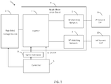
FIG. 1 shows a block diagram of a multi-mode wireless power transmitter. -
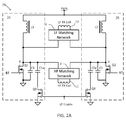
FIG. 2A shows an example of a multi-mode wireless power transmitter in which the multi-mode drive circuit is implemented by a class E differential amplifier. -
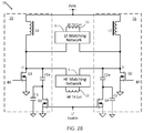
FIG. 2B shows another example in which the multi-mode drive circuit is implemented by a class E differential amplifier. -
FIGS. 3A and 3B show transistor drain voltage waveforms for the transistors of the class E amplifier ofFIG. 2A . -
FIG. 4 shows an embodiment similar toFIG. 2A , in which an inductor can be connected to or disconnected from the multi-mode drive circuit. -
FIG. 5 shows a method of wireless power transmission, according to some embodiments. - The inventors have recognized and appreciated that a multi-mode wireless power transmitter capable of transmitting wireless power at different frequencies can facilitate providing power to different types of wireless power receivers designed to operate at different frequencies. Such a multi-mode wireless power transmitter can allow providing power to a wider variety of electronic devices. For example, in some embodiments a multi-mode wireless power transmitter can be configured to provide power to both MI and MR receivers. In some embodiments, a multi-mode wireless power transmitter can provide power to devices that are designed according to a variety of different wireless charging specifications, such as the Qi standard promulgated by WPC, and other specifications designed for wireless power delivery at other frequencies, such as specifications for MR receivers, or other MI specifications. Such a multi-mode wireless power transmitter can support different types of receivers, enabling consumers to avoid the need to make a choice between different wireless power specifications, and can reduce or eliminate the need to acquire multiple wireless transmitters to power devices that receive wireless power at different frequencies.
- Described herein are embodiments of wireless power transmitters that include a resonant drive circuit that can be dynamically tuned to drive wireless power transmission at different frequencies. The resonant drive circuit includes an LC network that resonates at a frequency determined by the magnitude of the inductance and capacitance. In some embodiments, the resonant capacitance and/or the inductance is modified to facilitate wireless power transmission at different frequencies.
-
FIG. 1 shows a block diagram of a multi-modewireless power transmitter 1 in which amulti-mode drive circuit 7 has aninverter 3 that can be switched into different modes of operation for wireless transmission at different frequencies. For example, themulti-mode drive circuit 7 can be switched into a low frequency mode for driving a lowfrequency transmit coil 10 via a lowfrequency matching network 6, or a high frequency mode for driving a highfrequency transmit coil 12 via a highfrequency matching network 8. The multi-modewireless power transmitter 1 may include a regulated voltage source 2 (e.g., a voltage regulator) that provides a regulated DC voltage to theinverter 3. The regulatedvoltage source 2 produces a regulated DC output voltage in response to control stimulus from thecontroller 5. Themulti-mode drive circuit 7 may be a class E amplifier that converts the DC voltage at the input ofinverter 3 into an AC output voltage to drive the lowfrequency transmit coil 10 or highfrequency transmit coil 12. Producing an AC output voltage enables wireless power transmission through electromagnetic induction. -
Inverter 3 may be controlled to operate in different modes bycontroller 5. Thecontroller 5 of the multi-modewireless power transmitter 1 may control a signal generator 9 to drive theinverter 3 with signals of a selected wireless power transmission frequency. As an example for a low frequency mode of operation, to transmit power to a receiver designed to receive wireless power according to the Qi specification theinverter 3 may be switched at a frequency between 100 and 205 kHz for low power Qi receivers and 80-300 kHz for medium power Qi receivers. As an example for a high frequency mode of operation, to transmit power to a receiver designed to receive wireless power using MR technology, theinverter 3 may be switched at a higher frequency, such as a frequency of greater than 1 MHz, within an ISM band, e.g., 6.765 MHz to 6.795 MHz. However, these frequencies are described merely by way of example, as wireless power may be transmitted at a variety of suitable frequencies, in accordance with any suitable specification. - In some embodiments,
multi-mode drive circuit 7 may be designed to minimize or otherwise reduce switching power losses. Switching power losses are incurred in a switch when there is a non-zero voltage across the switch and it is turned on or off, which dissipates or charges the switch's parasitic capacitance. Switching power losses are proportional to frequency, and therefore are more severe at high frequencies. Switching losses can be minimized or reduced by using an inverter that is designed to turn the switch on or off when the voltage across the switch is zero or close to zero. Such a technique is termed "zero-voltage switching." - In some embodiments, the
multi-mode drive circuit 7 may be a class E amplifier. A class E amplifier may use LC resonance to cause the voltage across a switch to ring down to zero or approximately zero by the time the switch switches, which can achieve or approximate zero-voltage switching. However, the techniques described herein are not limited to use of a class E amplifier formulti-mode drive circuit 7, as another suitable amplifier configuration may be used, such as another type of resonant amplifier. Themulti-mode drive circuit 7 may be a single-ended amplifier or a differential amplifier, as the techniques described herein are not limited in this respect. -
Multi-mode drive circuit 7 may be a multi-mode amplifier that can be switched into a different modes of operation by modifying its resonant frequency. In a low frequency mode of operation, themulti-mode drive circuit 7 is tuned to a relatively low resonant frequency by adjusting a variable capacitance and/or inductance of themulti-mode drive circuit 7. In a high frequency mode of operation, themulti-mode drive circuit 7 is tuned to a relatively high resonant frequency by adjusting the variable capacitance and/or inductance of themulti-mode drive circuit 7. Examples of circuits that can adjust the variable capacitance and/or inductancemulti-mode drive circuit 7 are discussed with respect toFIGS. 2 and4 . - One or
more matching networks inverter 3. The matching network(s) may have one or more capacitive or inductive elements or any suitable combination of capacitive and inductive elements. Since the transmit coils may have an inductive impedance, in some embodiments the matching network(s) may include one or more capacitive elements, which, when combined with the impedance(s) of a transmit coil, presents an impedance to the output ofinverter 3 suitable for driving the respective transmit coil. In some embodiments, the resonant frequency of thematching networks inverter 3. - The transmit coils 10, 12 may be realized by any suitable type of conductors. The conductors may be wires, including solid wire or Litz wire, or patterned conductors, such as patterned conductors of a PC board or an integrated circuit.
-
Controller 5 may be an analog circuit or a digital circuit.Controller 5 may be programmable, and may command signal generator 9 to produce signals at a desired transmission frequency based on stored program instructions, so thatinverter 3 switches at the desired transmission frequency. -
FIG. 2A shows an example in which themulti-mode drive circuit 7A is implemented by a class E differential amplifier. Theinverter 3A includes transistors Q1 and Q2, inductors L1 and L2, capacitors C1 and C2, capacitors C1a and C2a and transistors Q3 and Q4. - In a low frequency mode of operation of
multi-mode drive circuit 7A, transistors Q3 and Q4 are turned on (conductive) by setting the signal LF Enable high, which connects capacitor C1a in parallel with C1 and connects capacitor C2a in parallel with C2, and thus increases the capacitance that resonates with inductor L1 and L2, which reduces the resonant frequency of theinverter 3A. Signal generator 9 produces signals ϕ1 and ϕ2 that drive the transistors Q1 and Q2 at the selected transmission frequency, which differentially drives the low frequency transmitcoil 10 via the lowfrequency matching network 6. The highfrequency matching network 8 may have one or more components that have a high impedance at low transmit frequencies, which attenuates low frequency signals to inhibit them from driving the high frequency transmitcoil 12. - In a high frequency mode of operation of
multi-mode drive circuit 7A, transistors Q3 and Q4 are turned off (non-conductive) by setting the signal LF Enable low, which disconnects capacitors C1a and C2a from the circuit, and capacitor C1 resonates with inductor L1 (and capacitor C2 resonates with inductor L2) at a higher frequency. Signal generator 9 produces signals ϕ1 and ϕ2 that drive the transistors Q1 and Q2 at the selected (high) transmission frequency, which differentially drives the high frequency transmitcoil 12 via the highfrequency matching network 8. The lowfrequency matching network 6 may have one or more components that have a high impedance at high transmit frequencies, which attenuates high frequency signals to inhibit them from driving the low frequency transmitcoil 10. - Thus,
multi-mode drive circuit 7 may be tuned to different resonant frequencies suitable for driving wireless power transmission at different frequencies. In some embodiments,controller 5 and/or signal generator 9 may control activation of transistors Q3 and Q4 by producing the signal LF Enable based upon the selected switching frequency ofinverter 3, as illustrated inFIG. 1 . - In some embodiments, capacitor C1 has a lower capacitance than capacitor C1a and capacitor C2 has a lower capacitance than capacitor C2a. In some embodiments, the ratio of capacitance values of capacitor C1a to capacitor C1 is approximately (e.g., within plus or minus 10%) of the square root of the frequency ratio between the transmission frequencies for the high and low frequency modes of operation. As an example, if the high transmission frequency is 6.78 MHz and the low transmission frequency is 130 kHz, the ratio of capacitance values of capacitor C1a to capacitor C1 may be about 7.07, plus or minus 10%. The ratio of the ratio of capacitance values of capacitor C2a to capacitor C2 may be the same or approximately the same as the ratio of capacitance values of capacitor C1a to capacitor C1.
-
FIG. 2B shows another example in which themulti-mode drive circuit 7B is implemented by a class E differential amplifierMulti-mode drive circuit 7B is similar tomulti-mode drive circuit 7A, with the exception that capacitors C1 and C1a ofinverter 3B can be connected in series rather than in parallel. Transistor Q3 is connected in parallel with capacitor C1. Transistor Q3 turns on (conductive) to short out capacitor C1 in the low frequency mode of operation, when LF Enable is high. Transistor Q3 turns off (non-conductive) in the high frequency mode of operation, which causes capacitors C1 and C1a to be in series with one another. The series combination of capacitors C1 and C1a has a lower effective capacitance than capacitor C1a alone, thereby increasing the resonant frequency in the high frequency mode of operation. Transistor Q4 operates similarly. More specifically, transistor Q4 turns on (conductive) to short out capacitor C2 in the low frequency mode of operation, when LF Enable is high. Transistor Q4 turns off (non-conductive) in the high frequency mode of operation, which causes capacitors C2 and C2a to be in series with one another, the combination of which has a lower effective capacitance than capacitor C2a alone. -
FIG. 3A shows the drain voltage waveform of transistor Q1, according to some embodiments. When transistor Q1 is turned off (non-conductive), the drain (D) voltage rises sinusoidally due to the resonance between the inductor L1 and capacitance C1 (and C1a, for low frequency operation). When the drain voltage rings down to zero, transistor Q1 is turned on. Thus, transistor Q1 can operate with zero voltage switching, which can improve the efficiency of theinverter 3. Transistor Q2 operates similarly but phase shifted 180° with respect to transistor Q1. Transistor Q1 and Q2 each may be turned on with approximately 50% duty ratio.FIG. 3B shows the drain voltage waveform of transistor Q2, according to some embodiments. Since transistor Q2 is connected to the opposite terminal of the matching networks compared to Q1, transistor Q2 produces a pulse of opposite polarity, as seen by the matching networks. The drain voltages of transistors Q1 and Q2 differentially drive the low frequency transmitcoil 10 via the lowfrequency matching network 6 or the high frequency transmitcoil 12 via the highfrequency matching network 8. -
FIG. 4 shows an embodiment of amulti-mode drive circuit 7C in which the resonant inductance can be adjusted. As shown inFIG. 4 ,inverter 3C has switches S1 and S2 in parallel with inductors L1a and L2a, respectively. Switches S1 and S2 may be controlled by the complement of the LF Enable signal.Switches S 1 and S2 can be realized by mechanical or solid state AC switches, or any other suitable switches. When a low frequency signal is transmitted, switchesS 1 and S2 are turned off (non-conductive) by the LF Enable signal being set high, and inductors L1a and L2a are included in the resonant inductance, thereby lowering the resonant frequency. When a high frequency signal is transmitted, switchesS 1 and S2 are turned on by the LF Enable signal being set low, shorting out inductors L1a and L2a, thereby increasing the resonant frequency. Shorting out inductors L1a and L2a can also increase efficiency, as conduction losses due to the equivalent series resistance (ESR) of inductors L1a and L2a is removed when inductors L1a and L2a are shorted. - In the embodiment of
FIG. 4 , the capacitors C1, C1a and Q3 (as well as C2, C2a and Q4) are shown as connected in a configuration as illustrated inFIG. 2A . However, in some embodiments the capacitors C1, C1a and Q3 (as well as C2, C2a and Q4) of theinverter 3C may be connected in a configuration as illustrated inFIG. 2B . - As discussed above, a variety of wireless power receivers are being designed which can receive wireless power at different frequencies. In some embodiments, the multi-mode wireless power transmitter may detect the type of receiver that is present in the vicinity of the multi-mode wireless power transmitter, either through wireless communication with the receiver or another technique. For example, the multi-mode wireless power transmitter may detect or otherwise determine the wireless power specification used by the receiver. Such a determination may be made by the
controller 5 of the multi-mode wireless power transmitter, in some embodiments.Controller 5 may then produce signals at the frequency suitable for wirelessly delivering power to the detected receiver. -
FIG. 5 shows a flowchart of a method of wireless power transmission at different frequencies, according to some embodiments. In step S1, a wireless power receiver is detected that is capable of receiving wireless power. The wireless power transmitter communicates with the wireless power receiver to determine the frequency at which the wireless power receiver is capable of receiving wireless power. In step S2, thecontroller 5 controls themulti-mode drive circuit 7 to have a resonant frequency suitable for wireless power transmission to the receiver at the determined frequency. For example, as discussed above, if the detected wireless power receiver is capable of receiving power at a low frequency, thecontroller 5 may activate the LF Enable signal. In step S3, themulti-mode drive circuit 7 drives wireless power transmission to the receiver at the determined frequency. Subsequently, if another wireless power receiver is detected in the vicinity of the multi-mode wireless power transmitter that receives power at a different frequency, the multi-mode wireless power transmitter may determine another transmission frequency suitable for transmitting power to the newly-detected receiver in step S4. In step S5, thecontroller 5 controls themulti-mode drive circuit 7 to have a resonant frequency suitable for wireless power transmission to the receiver at the determined frequency of the newly-detected receiver. For example, as discussed above, if the newly-detected wireless power receiver is capable of receiving power at a high frequency, thecontroller 5 may deactivate the LF enable signal. In step S6, themulti-mode drive circuit 7 drives wireless power transmission to the newly-detected receiver at the determined frequency. - In some embodiments, a multi-mode wireless power transmitter may operate at more than two transmission frequencies or frequency bands. If so, the
multi-mode drive circuit 7 may be configured to tune the resonant frequency to one or more additional frequencies. To allow tuning to additional frequencies, additional capacitors C1a, C2a and switches such as Q3, Q4 may be added in parallel with capacitors C1 and C2, respectively. - As discussed above, a multi-mode wireless power transmitter may be controlled using
controller 5, which may be implemented by any suitable type of circuitry. For example, thecontroller 5 may be implemented using hardware or a combination of hardware and software. When implemented using software, suitable software code can be executed on any suitable processor (e.g., a microprocessor) or collection of processors. The one or more controllers can be implemented in numerous ways, such as with dedicated hardware, or with general purpose hardware (e.g., one or more processors) that is programmed using microcode or software to perform the functions recited above. - Various aspects of the apparatus and techniques described herein may be used alone, in combination, or in a variety of arrangements not specifically discussed in the embodiments described in the foregoing description and is therefore not limited in its application to the details and arrangement of components set forth in the foregoing description or illustrated in the drawings. For example, aspects described in one embodiment may be combined in any manner with aspects described in other embodiments.
- Use of ordinal terms such as "first," "second," "third," etc., in the claims to modify a claim element does not by itself connote any priority, precedence, or order of one claim element over another or the temporal order in which acts of a method are performed, but are used merely as labels to distinguish one claim element having a certain name from another element having a same name (but for use of the ordinal term) to distinguish the claim elements.
- Also, the phraseology and terminology used herein is for the purpose of description and should not be regarded as limiting. The use of "including," "comprising," or "having," "containing," "involving," and variations thereof herein, is meant to encompass the items listed thereafter and equivalents thereof as well as additional items.
Claims (15)
- A wireless power transmitter, comprising:a multi-mode drive circuit having a controllable resonant frequency, the multi-mode drive circuit being controlled to have a first resonant frequency to drive wireless power transmission at a first transmit frequency, and being controlled to have a second resonant frequency higher than the first resonant frequency to drive wireless power transmission at a second transmit frequency higher than the first transmit frequency.
- The wireless power transmitter of claim 1, wherein the multi-mode drive circuit comprises an inverter, optionally a class E amplifier.
- The wireless power transmitter of any preceding claim, wherein the multi-mode drive circuit has a variable capacitance that is controlled to change the controllable resonant frequency.
- The wireless power transmitter of claim 3, wherein the multi-mode drive circuit comprises:a capacitor; anda switch controlled to connect or disconnect the capacitor to control whether the capacitor contributes to the variable capacitance.
- The wireless power transmitter of any preceding claim, wherein the multi-mode drive circuit has a variable inductance that is controlled based on a mode of operation of the multi-mode drive circuit.
- The wireless power transmitter of claim 5, wherein the multi-mode drive circuit comprises:an inductor; anda switch controlled to connect or disconnect the inductor to control whether the inductor contributes to the variable inductance.
- The wireless power transmitter of claim 6, wherein the switch connects the inductor so that the inductor contributes to the variable inductance when the multi-mode drive circuit is controlled to drive wireless power transmission at the first transmit frequency.
- The wireless power transmitter of claim 6 or 7, wherein the switch disconnects the inductor so that the inductor does not contribute to the variable inductance when the multi-mode drive circuit is controlled to drive wireless power transmission at the second transmit frequency.
- The wireless power transmitter of any preceding claim, wherein the first transmit frequency is lower than 300 kHz, the second transmit frequency is higher than 1 MHz, and optionally the second transmit frequency is between 6.765 MHz and 6.795 MHz.
- The wireless power transmitter of any preceding claim, further comprising:a first transmit coil coupled to the multi-mode drive circuit to transmit wireless power at the first transmit frequency; anda second transmit coil coupled to the multi-mode drive circuit to transmit wireless power at the second transmit frequency.
- A wireless power transmission method, comprising:(A) controlling a multi-mode drive circuit having a controllable resonant frequency to have a first resonant frequency to drive wireless power transmission at a first transmit frequency; and(B) controlling the multi-mode drive circuit to have a second resonant frequency higher than the first resonant frequency to drive wireless power transmission at a second transmit frequency higher than the first transmit frequency.
- The wireless power transmission method of claim 11, further comprising changing a variable capacitance of the multi-mode drive circuit to change the controllable resonant frequency.
- The wireless power transmission method of claim 12, wherein the variable capacitance is changed by a switch that is controlled to connect or disconnect a capacitor to control whether the capacitor contributes to the variable capacitance.
- The wireless power transmission method of any one of claims 11-13, further comprising changing a variable inductance of the multi-mode drive circuit.
- The wireless power transmission method of any one of claims 11-14, further comprising switching between (A) and (B) in response to detection of a wireless power receiver that can receive power at the first transmit frequency or the second transmit frequency.
Applications Claiming Priority (2)
| Application Number | Priority Date | Filing Date | Title |
|---|---|---|---|
| US201562193803P | 2015-07-17 | 2015-07-17 | |
| US14/990,833 US10291036B2 (en) | 2015-07-17 | 2016-01-08 | Multi-mode resonant wireless power transmitter |
Publications (2)
| Publication Number | Publication Date |
|---|---|
| EP3142211A1 true EP3142211A1 (en) | 2017-03-15 |
| EP3142211B1 EP3142211B1 (en) | 2022-11-02 |
Family
ID=57776448
Family Applications (1)
| Application Number | Title | Priority Date | Filing Date |
|---|---|---|---|
| EP16179120.7A Active EP3142211B1 (en) | 2015-07-17 | 2016-07-12 | Multi-mode resonant wireless power transmitter |
Country Status (3)
| Country | Link |
|---|---|
| US (1) | US10291036B2 (en) |
| EP (1) | EP3142211B1 (en) |
| CN (1) | CN106451816B (en) |
Families Citing this family (11)
| Publication number | Priority date | Publication date | Assignee | Title |
|---|---|---|---|---|
| EP3280030B1 (en) * | 2016-08-04 | 2023-08-30 | General Electric Company | System and method for charging receiver devices |
| SG10201705912TA (en) * | 2016-08-04 | 2018-03-28 | Gen Electric | System and method for charging receiver devices |
| US10608471B2 (en) * | 2016-09-16 | 2020-03-31 | Integrated Device Technology, Inc. | Multimode wireless power receiver circuit |
| US10637293B2 (en) * | 2016-09-30 | 2020-04-28 | University Of Tennessee Research Foundation | Dual-frequency mode transmitter for wireless power transfer |
| EP3346581B1 (en) * | 2017-01-04 | 2023-06-14 | LG Electronics Inc. | Wireless charger for mobile terminal in vehicle |
| CN118232544A (en) | 2017-05-30 | 2024-06-21 | 通用电气公司 | Wireless charging device, receiver device and operation method thereof |
| CN107634585A (en) * | 2017-09-11 | 2018-01-26 | 深圳市华宝新能源股份有限公司 | A kind of wireless power transmission and receiving circuit and device |
| CN112018907B (en) * | 2020-10-14 | 2021-04-06 | 广东希荻微电子股份有限公司 | Charging module and dual-mode wireless charging system |
| CN112578465B (en) * | 2020-12-02 | 2025-05-20 | 熵基科技股份有限公司 | Dual-frenquency detection circuitry and dual-frenquency security inspection door |
| TWI794795B (en) * | 2021-04-26 | 2023-03-01 | 國立陽明交通大學 | Inductive resonant wireless charging system, resonant wireless charging transmitting device, wireless charging relay device and inductive wireless charging receiving device |
| JP7782569B2 (en) * | 2021-10-11 | 2025-12-09 | Ntt株式会社 | Antenna device and contactless power transmission system |
Citations (3)
| Publication number | Priority date | Publication date | Assignee | Title |
|---|---|---|---|---|
| US20120038220A1 (en) * | 2010-08-13 | 2012-02-16 | Samsung Electro-Mechanics Co., Ltd. | Wireless power transmission apparatus and transmission method thereof |
| WO2014191609A1 (en) * | 2013-05-31 | 2014-12-04 | Nokia Corporation | A multi-coil wireless power apparatus |
| US20150115727A1 (en) * | 2013-10-31 | 2015-04-30 | Qualcomm Incorporated | Systems, apparatus, and method for a dual mode wireless power receiver |
Family Cites Families (13)
| Publication number | Priority date | Publication date | Assignee | Title |
|---|---|---|---|---|
| WO2009089253A1 (en) * | 2008-01-07 | 2009-07-16 | Access Business Group International Llc | Inductive power supply with duty cycle control |
| JP4911148B2 (en) * | 2008-09-02 | 2012-04-04 | ソニー株式会社 | Contactless power supply |
| JP5365306B2 (en) | 2009-03-31 | 2013-12-11 | 富士通株式会社 | Wireless power supply system |
| JP2010252468A (en) * | 2009-04-14 | 2010-11-04 | Sony Corp | Power transmission device and method, power reception device and method, and power transmission system |
| NZ588159A (en) | 2010-09-23 | 2014-01-31 | Powerbyproxi Ltd | A contactless power transfer system |
| KR20120051320A (en) * | 2010-11-12 | 2012-05-22 | 한국전자통신연구원 | Wireless energy transfer device |
| JP2013013204A (en) * | 2011-06-28 | 2013-01-17 | Toshiba Corp | Wireless power transmission system, power transmission device and power reception device |
| US9444289B2 (en) * | 2011-09-09 | 2016-09-13 | Lg Electronics Inc. | Wireless power system and resonant frequency changing method thereof |
| US9818530B2 (en) * | 2012-01-17 | 2017-11-14 | Texas Instruments Incorporated | Adaptive wireless power transfer system and method |
| US10320234B2 (en) * | 2013-08-02 | 2019-06-11 | Integrated Device Technology, Inc. | Multimode wireless power receivers and related methods |
| US10122212B2 (en) | 2013-08-30 | 2018-11-06 | Samsung Electro-Mechanics Co., Ltd. | Power supply device |
| JP6242311B2 (en) * | 2013-10-29 | 2017-12-06 | パナソニック株式会社 | Wireless power transmission apparatus and wireless power transmission system |
| US10135303B2 (en) * | 2014-05-19 | 2018-11-20 | Apple Inc. | Operating a wireless power transfer system at multiple frequencies |
-
2016
- 2016-01-08 US US14/990,833 patent/US10291036B2/en active Active
- 2016-07-12 EP EP16179120.7A patent/EP3142211B1/en active Active
- 2016-07-15 CN CN201610559922.5A patent/CN106451816B/en active Active
Patent Citations (3)
| Publication number | Priority date | Publication date | Assignee | Title |
|---|---|---|---|---|
| US20120038220A1 (en) * | 2010-08-13 | 2012-02-16 | Samsung Electro-Mechanics Co., Ltd. | Wireless power transmission apparatus and transmission method thereof |
| WO2014191609A1 (en) * | 2013-05-31 | 2014-12-04 | Nokia Corporation | A multi-coil wireless power apparatus |
| US20150115727A1 (en) * | 2013-10-31 | 2015-04-30 | Qualcomm Incorporated | Systems, apparatus, and method for a dual mode wireless power receiver |
Also Published As
| Publication number | Publication date |
|---|---|
| CN106451816A (en) | 2017-02-22 |
| CN106451816B (en) | 2019-08-09 |
| EP3142211B1 (en) | 2022-11-02 |
| US20170018937A1 (en) | 2017-01-19 |
| US10291036B2 (en) | 2019-05-14 |
Similar Documents
| Publication | Publication Date | Title |
|---|---|---|
| EP3142211B1 (en) | Multi-mode resonant wireless power transmitter | |
| US11677273B2 (en) | Drive circuits for multi-mode wireless power transmitter | |
| EP3155706B1 (en) | Multi-mode wireless power transmitter | |
| US10193389B2 (en) | Multi-bridge topology | |
| US9923384B2 (en) | Method for performing efficiency optimization of an electronic device, and associated apparatus | |
| US11316372B2 (en) | Driving circuit and wireless power transmitter including the same | |
| CN105281441B (en) | Wireless power transmitter and Wireless power transmission system | |
| CN109904884B (en) | Wireless charging method, device, terminal, storage medium and electronic device | |
| EP2953235A1 (en) | Wireless power transfer system, power receiver, and wireless power transfer method | |
| KR101837121B1 (en) | Dual band Wireless Power Receiving Unit | |
| CN108370240B (en) | Class E2 amplifier | |
| WO2015097809A1 (en) | Resonant transmitting power-supply device and resonant transmitting power-supply system | |
| US20180083473A1 (en) | Variable capacitor series tuning configuration | |
| US20160308393A1 (en) | Contactless power receiver and method for operating same | |
| JP2013074756A (en) | Wireless power receiver, wireless power feeder, and wireless power feeding system | |
| US10608471B2 (en) | Multimode wireless power receiver circuit | |
| KR20160121698A (en) | Apparatus and Method for wireless power transmission capable of frequency selection for LED panel | |
| US20180083472A1 (en) | Variable capacitor speed up circuit | |
| US20250088033A1 (en) | Magnetic cover and methods and apparatus to detect positioning of the magnetic cover over a wireless charging transmitter | |
| EP4554047A1 (en) | Electronic device and method for wireless charging supporting multiple frequencies, and non-transitory storage medium | |
| US12401227B1 (en) | Inductive power transfer system with common mode channel communication |
Legal Events
| Date | Code | Title | Description |
|---|---|---|---|
| PUAI | Public reference made under article 153(3) epc to a published international application that has entered the european phase |
Free format text: ORIGINAL CODE: 0009012 |
|
| STAA | Information on the status of an ep patent application or granted ep patent |
Free format text: STATUS: THE APPLICATION HAS BEEN PUBLISHED |
|
| AK | Designated contracting states |
Kind code of ref document: A1 Designated state(s): AL AT BE BG CH CY CZ DE DK EE ES FI FR GB GR HR HU IE IS IT LI LT LU LV MC MK MT NL NO PL PT RO RS SE SI SK SM TR |
|
| AX | Request for extension of the european patent |
Extension state: BA ME |
|
| STAA | Information on the status of an ep patent application or granted ep patent |
Free format text: STATUS: REQUEST FOR EXAMINATION WAS MADE |
|
| 17P | Request for examination filed |
Effective date: 20170914 |
|
| RBV | Designated contracting states (corrected) |
Designated state(s): AL AT BE BG CH CY CZ DE DK EE ES FI FR GB GR HR HU IE IS IT LI LT LU LV MC MK MT NL NO PL PT RO RS SE SI SK SM TR |
|
| STAA | Information on the status of an ep patent application or granted ep patent |
Free format text: STATUS: EXAMINATION IS IN PROGRESS |
|
| 17Q | First examination report despatched |
Effective date: 20190320 |
|
| RAP1 | Party data changed (applicant data changed or rights of an application transferred) |
Owner name: MEDIATEK INC. |
|
| RIC1 | Information provided on ipc code assigned before grant |
Ipc: H02J 50/80 20160101ALN20211118BHEP Ipc: H02J 50/40 20160101ALI20211118BHEP Ipc: H02J 50/12 20160101AFI20211118BHEP |
|
| RIC1 | Information provided on ipc code assigned before grant |
Ipc: H02J 50/80 20160101ALN20211207BHEP Ipc: H02J 50/40 20160101ALI20211207BHEP Ipc: H02J 50/12 20160101AFI20211207BHEP |
|
| GRAP | Despatch of communication of intention to grant a patent |
Free format text: ORIGINAL CODE: EPIDOSNIGR1 |
|
| STAA | Information on the status of an ep patent application or granted ep patent |
Free format text: STATUS: GRANT OF PATENT IS INTENDED |
|
| INTG | Intention to grant announced |
Effective date: 20220119 |
|
| GRAJ | Information related to disapproval of communication of intention to grant by the applicant or resumption of examination proceedings by the epo deleted |
Free format text: ORIGINAL CODE: EPIDOSDIGR1 |
|
| STAA | Information on the status of an ep patent application or granted ep patent |
Free format text: STATUS: EXAMINATION IS IN PROGRESS |
|
| REG | Reference to a national code |
Ref country code: DE Ref legal event code: R079 Ref document number: 602016076014 Country of ref document: DE Free format text: PREVIOUS MAIN CLASS: H02J0005000000 Ipc: H02J0050120000 |
|
| INTC | Intention to grant announced (deleted) | ||
| GRAP | Despatch of communication of intention to grant a patent |
Free format text: ORIGINAL CODE: EPIDOSNIGR1 |
|
| STAA | Information on the status of an ep patent application or granted ep patent |
Free format text: STATUS: GRANT OF PATENT IS INTENDED |
|
| RIC1 | Information provided on ipc code assigned before grant |
Ipc: H02J 50/80 20160101ALN20220609BHEP Ipc: H02J 50/40 20160101ALI20220609BHEP Ipc: H02J 50/12 20160101AFI20220609BHEP |
|
| INTG | Intention to grant announced |
Effective date: 20220629 |
|
| GRAS | Grant fee paid |
Free format text: ORIGINAL CODE: EPIDOSNIGR3 |
|
| GRAA | (expected) grant |
Free format text: ORIGINAL CODE: 0009210 |
|
| STAA | Information on the status of an ep patent application or granted ep patent |
Free format text: STATUS: THE PATENT HAS BEEN GRANTED |
|
| AK | Designated contracting states |
Kind code of ref document: B1 Designated state(s): AL AT BE BG CH CY CZ DE DK EE ES FI FR GB GR HR HU IE IS IT LI LT LU LV MC MK MT NL NO PL PT RO RS SE SI SK SM TR |
|
| REG | Reference to a national code |
Ref country code: GB Ref legal event code: FG4D |
|
| REG | Reference to a national code |
Ref country code: CH Ref legal event code: EP Ref country code: AT Ref legal event code: REF Ref document number: 1529484 Country of ref document: AT Kind code of ref document: T Effective date: 20221115 |
|
| REG | Reference to a national code |
Ref country code: DE Ref legal event code: R096 Ref document number: 602016076014 Country of ref document: DE |
|
| REG | Reference to a national code |
Ref country code: IE Ref legal event code: FG4D |
|
| REG | Reference to a national code |
Ref country code: LT Ref legal event code: MG9D |
|
| REG | Reference to a national code |
Ref country code: NL Ref legal event code: MP Effective date: 20221102 |
|
| REG | Reference to a national code |
Ref country code: AT Ref legal event code: MK05 Ref document number: 1529484 Country of ref document: AT Kind code of ref document: T Effective date: 20221102 |
|
| PG25 | Lapsed in a contracting state [announced via postgrant information from national office to epo] |
Ref country code: SE Free format text: LAPSE BECAUSE OF FAILURE TO SUBMIT A TRANSLATION OF THE DESCRIPTION OR TO PAY THE FEE WITHIN THE PRESCRIBED TIME-LIMIT Effective date: 20221102 Ref country code: PT Free format text: LAPSE BECAUSE OF FAILURE TO SUBMIT A TRANSLATION OF THE DESCRIPTION OR TO PAY THE FEE WITHIN THE PRESCRIBED TIME-LIMIT Effective date: 20230302 Ref country code: NO Free format text: LAPSE BECAUSE OF FAILURE TO SUBMIT A TRANSLATION OF THE DESCRIPTION OR TO PAY THE FEE WITHIN THE PRESCRIBED TIME-LIMIT Effective date: 20230202 Ref country code: LT Free format text: LAPSE BECAUSE OF FAILURE TO SUBMIT A TRANSLATION OF THE DESCRIPTION OR TO PAY THE FEE WITHIN THE PRESCRIBED TIME-LIMIT Effective date: 20221102 Ref country code: FI Free format text: LAPSE BECAUSE OF FAILURE TO SUBMIT A TRANSLATION OF THE DESCRIPTION OR TO PAY THE FEE WITHIN THE PRESCRIBED TIME-LIMIT Effective date: 20221102 Ref country code: ES Free format text: LAPSE BECAUSE OF FAILURE TO SUBMIT A TRANSLATION OF THE DESCRIPTION OR TO PAY THE FEE WITHIN THE PRESCRIBED TIME-LIMIT Effective date: 20221102 Ref country code: AT Free format text: LAPSE BECAUSE OF FAILURE TO SUBMIT A TRANSLATION OF THE DESCRIPTION OR TO PAY THE FEE WITHIN THE PRESCRIBED TIME-LIMIT Effective date: 20221102 |
|
| PG25 | Lapsed in a contracting state [announced via postgrant information from national office to epo] |
Ref country code: RS Free format text: LAPSE BECAUSE OF FAILURE TO SUBMIT A TRANSLATION OF THE DESCRIPTION OR TO PAY THE FEE WITHIN THE PRESCRIBED TIME-LIMIT Effective date: 20221102 Ref country code: PL Free format text: LAPSE BECAUSE OF FAILURE TO SUBMIT A TRANSLATION OF THE DESCRIPTION OR TO PAY THE FEE WITHIN THE PRESCRIBED TIME-LIMIT Effective date: 20221102 Ref country code: LV Free format text: LAPSE BECAUSE OF FAILURE TO SUBMIT A TRANSLATION OF THE DESCRIPTION OR TO PAY THE FEE WITHIN THE PRESCRIBED TIME-LIMIT Effective date: 20221102 Ref country code: IS Free format text: LAPSE BECAUSE OF FAILURE TO SUBMIT A TRANSLATION OF THE DESCRIPTION OR TO PAY THE FEE WITHIN THE PRESCRIBED TIME-LIMIT Effective date: 20230302 Ref country code: HR Free format text: LAPSE BECAUSE OF FAILURE TO SUBMIT A TRANSLATION OF THE DESCRIPTION OR TO PAY THE FEE WITHIN THE PRESCRIBED TIME-LIMIT Effective date: 20221102 Ref country code: GR Free format text: LAPSE BECAUSE OF FAILURE TO SUBMIT A TRANSLATION OF THE DESCRIPTION OR TO PAY THE FEE WITHIN THE PRESCRIBED TIME-LIMIT Effective date: 20230203 |
|
| PG25 | Lapsed in a contracting state [announced via postgrant information from national office to epo] |
Ref country code: NL Free format text: LAPSE BECAUSE OF FAILURE TO SUBMIT A TRANSLATION OF THE DESCRIPTION OR TO PAY THE FEE WITHIN THE PRESCRIBED TIME-LIMIT Effective date: 20221102 |
|
| P01 | Opt-out of the competence of the unified patent court (upc) registered |
Effective date: 20230607 |
|
| PG25 | Lapsed in a contracting state [announced via postgrant information from national office to epo] |
Ref country code: SM Free format text: LAPSE BECAUSE OF FAILURE TO SUBMIT A TRANSLATION OF THE DESCRIPTION OR TO PAY THE FEE WITHIN THE PRESCRIBED TIME-LIMIT Effective date: 20221102 Ref country code: RO Free format text: LAPSE BECAUSE OF FAILURE TO SUBMIT A TRANSLATION OF THE DESCRIPTION OR TO PAY THE FEE WITHIN THE PRESCRIBED TIME-LIMIT Effective date: 20221102 Ref country code: EE Free format text: LAPSE BECAUSE OF FAILURE TO SUBMIT A TRANSLATION OF THE DESCRIPTION OR TO PAY THE FEE WITHIN THE PRESCRIBED TIME-LIMIT Effective date: 20221102 Ref country code: DK Free format text: LAPSE BECAUSE OF FAILURE TO SUBMIT A TRANSLATION OF THE DESCRIPTION OR TO PAY THE FEE WITHIN THE PRESCRIBED TIME-LIMIT Effective date: 20221102 Ref country code: CZ Free format text: LAPSE BECAUSE OF FAILURE TO SUBMIT A TRANSLATION OF THE DESCRIPTION OR TO PAY THE FEE WITHIN THE PRESCRIBED TIME-LIMIT Effective date: 20221102 |
|
| REG | Reference to a national code |
Ref country code: DE Ref legal event code: R097 Ref document number: 602016076014 Country of ref document: DE |
|
| PG25 | Lapsed in a contracting state [announced via postgrant information from national office to epo] |
Ref country code: SK Free format text: LAPSE BECAUSE OF FAILURE TO SUBMIT A TRANSLATION OF THE DESCRIPTION OR TO PAY THE FEE WITHIN THE PRESCRIBED TIME-LIMIT Effective date: 20221102 Ref country code: AL Free format text: LAPSE BECAUSE OF FAILURE TO SUBMIT A TRANSLATION OF THE DESCRIPTION OR TO PAY THE FEE WITHIN THE PRESCRIBED TIME-LIMIT Effective date: 20221102 |
|
| PLBE | No opposition filed within time limit |
Free format text: ORIGINAL CODE: 0009261 |
|
| STAA | Information on the status of an ep patent application or granted ep patent |
Free format text: STATUS: NO OPPOSITION FILED WITHIN TIME LIMIT |
|
| 26N | No opposition filed |
Effective date: 20230803 |
|
| PG25 | Lapsed in a contracting state [announced via postgrant information from national office to epo] |
Ref country code: SI Free format text: LAPSE BECAUSE OF FAILURE TO SUBMIT A TRANSLATION OF THE DESCRIPTION OR TO PAY THE FEE WITHIN THE PRESCRIBED TIME-LIMIT Effective date: 20221102 |
|
| PG25 | Lapsed in a contracting state [announced via postgrant information from national office to epo] |
Ref country code: MC Free format text: LAPSE BECAUSE OF FAILURE TO SUBMIT A TRANSLATION OF THE DESCRIPTION OR TO PAY THE FEE WITHIN THE PRESCRIBED TIME-LIMIT Effective date: 20221102 |
|
| PG25 | Lapsed in a contracting state [announced via postgrant information from national office to epo] |
Ref country code: MC Free format text: LAPSE BECAUSE OF FAILURE TO SUBMIT A TRANSLATION OF THE DESCRIPTION OR TO PAY THE FEE WITHIN THE PRESCRIBED TIME-LIMIT Effective date: 20221102 |
|
| REG | Reference to a national code |
Ref country code: CH Ref legal event code: PL |
|
| REG | Reference to a national code |
Ref country code: BE Ref legal event code: MM Effective date: 20230731 |
|
| PG25 | Lapsed in a contracting state [announced via postgrant information from national office to epo] |
Ref country code: LU Free format text: LAPSE BECAUSE OF NON-PAYMENT OF DUE FEES Effective date: 20230712 |
|
| PG25 | Lapsed in a contracting state [announced via postgrant information from national office to epo] |
Ref country code: LU Free format text: LAPSE BECAUSE OF NON-PAYMENT OF DUE FEES Effective date: 20230712 |
|
| REG | Reference to a national code |
Ref country code: IE Ref legal event code: MM4A |
|
| PG25 | Lapsed in a contracting state [announced via postgrant information from national office to epo] |
Ref country code: CH Free format text: LAPSE BECAUSE OF NON-PAYMENT OF DUE FEES Effective date: 20230731 |
|
| PG25 | Lapsed in a contracting state [announced via postgrant information from national office to epo] |
Ref country code: IT Free format text: LAPSE BECAUSE OF FAILURE TO SUBMIT A TRANSLATION OF THE DESCRIPTION OR TO PAY THE FEE WITHIN THE PRESCRIBED TIME-LIMIT Effective date: 20221102 Ref country code: BE Free format text: LAPSE BECAUSE OF NON-PAYMENT OF DUE FEES Effective date: 20230731 |
|
| PG25 | Lapsed in a contracting state [announced via postgrant information from national office to epo] |
Ref country code: IE Free format text: LAPSE BECAUSE OF NON-PAYMENT OF DUE FEES Effective date: 20230712 |
|
| PG25 | Lapsed in a contracting state [announced via postgrant information from national office to epo] |
Ref country code: IE Free format text: LAPSE BECAUSE OF NON-PAYMENT OF DUE FEES Effective date: 20230712 |
|
| PG25 | Lapsed in a contracting state [announced via postgrant information from national office to epo] |
Ref country code: BG Free format text: LAPSE BECAUSE OF FAILURE TO SUBMIT A TRANSLATION OF THE DESCRIPTION OR TO PAY THE FEE WITHIN THE PRESCRIBED TIME-LIMIT Effective date: 20221102 |
|
| PG25 | Lapsed in a contracting state [announced via postgrant information from national office to epo] |
Ref country code: BG Free format text: LAPSE BECAUSE OF FAILURE TO SUBMIT A TRANSLATION OF THE DESCRIPTION OR TO PAY THE FEE WITHIN THE PRESCRIBED TIME-LIMIT Effective date: 20221102 |
|
| PGFP | Annual fee paid to national office [announced via postgrant information from national office to epo] |
Ref country code: GB Payment date: 20250522 Year of fee payment: 10 |
|
| PGFP | Annual fee paid to national office [announced via postgrant information from national office to epo] |
Ref country code: FR Payment date: 20250508 Year of fee payment: 10 |
|
| PG25 | Lapsed in a contracting state [announced via postgrant information from national office to epo] |
Ref country code: CY Free format text: LAPSE BECAUSE OF FAILURE TO SUBMIT A TRANSLATION OF THE DESCRIPTION OR TO PAY THE FEE WITHIN THE PRESCRIBED TIME-LIMIT; INVALID AB INITIO Effective date: 20160712 |
|
| PG25 | Lapsed in a contracting state [announced via postgrant information from national office to epo] |
Ref country code: HU Free format text: LAPSE BECAUSE OF FAILURE TO SUBMIT A TRANSLATION OF THE DESCRIPTION OR TO PAY THE FEE WITHIN THE PRESCRIBED TIME-LIMIT; INVALID AB INITIO Effective date: 20160712 |
|
| PGFP | Annual fee paid to national office [announced via postgrant information from national office to epo] |
Ref country code: DE Payment date: 20250521 Year of fee payment: 10 |
|
| PG25 | Lapsed in a contracting state [announced via postgrant information from national office to epo] |
Ref country code: TR Free format text: LAPSE BECAUSE OF FAILURE TO SUBMIT A TRANSLATION OF THE DESCRIPTION OR TO PAY THE FEE WITHIN THE PRESCRIBED TIME-LIMIT Effective date: 20221102 |