EP3142150A1 - Partially biased isolation in semiconductor devices - Google Patents
Partially biased isolation in semiconductor devices Download PDFInfo
- Publication number
- EP3142150A1 EP3142150A1 EP16187929.1A EP16187929A EP3142150A1 EP 3142150 A1 EP3142150 A1 EP 3142150A1 EP 16187929 A EP16187929 A EP 16187929A EP 3142150 A1 EP3142150 A1 EP 3142150A1
- Authority
- EP
- European Patent Office
- Prior art keywords
- region
- isolation
- well region
- depleted
- doped
- Prior art date
- Legal status (The legal status is an assumption and is not a legal conclusion. Google has not performed a legal analysis and makes no representation as to the accuracy of the status listed.)
- Granted
Links
- 238000002955 isolation Methods 0.000 title claims abstract description 266
- 239000004065 semiconductor Substances 0.000 title claims abstract description 79
- 230000004888 barrier function Effects 0.000 claims abstract description 102
- 239000000758 substrate Substances 0.000 claims abstract description 99
- 210000000746 body region Anatomy 0.000 claims description 58
- 239000002019 doping agent Substances 0.000 claims description 51
- 238000002513 implantation Methods 0.000 claims description 45
- 238000000034 method Methods 0.000 claims description 27
- 239000002800 charge carrier Substances 0.000 claims description 15
- 238000004519 manufacturing process Methods 0.000 claims description 10
- 230000008878 coupling Effects 0.000 claims description 8
- 238000010168 coupling process Methods 0.000 claims description 8
- 238000005859 coupling reaction Methods 0.000 claims description 8
- 238000009792 diffusion process Methods 0.000 claims description 8
- 239000007943 implant Substances 0.000 description 30
- 229910052751 metal Inorganic materials 0.000 description 12
- 239000002184 metal Substances 0.000 description 12
- 230000015556 catabolic process Effects 0.000 description 11
- 230000015572 biosynthetic process Effects 0.000 description 8
- 125000006850 spacer group Chemical group 0.000 description 8
- 239000000463 material Substances 0.000 description 5
- 238000002161 passivation Methods 0.000 description 5
- 230000002093 peripheral effect Effects 0.000 description 5
- ALKWEXBKAHPJAQ-NAKRPEOUSA-N Asn-Leu-Asp-Asp Chemical compound NC(=O)C[C@H](N)C(=O)N[C@@H](CC(C)C)C(=O)N[C@@H](CC(O)=O)C(=O)N[C@@H](CC(O)=O)C(O)=O ALKWEXBKAHPJAQ-NAKRPEOUSA-N 0.000 description 4
- 230000000694 effects Effects 0.000 description 4
- 230000005684 electric field Effects 0.000 description 4
- 230000008569 process Effects 0.000 description 4
- VYPSYNLAJGMNEJ-UHFFFAOYSA-N Silicium dioxide Chemical compound O=[Si]=O VYPSYNLAJGMNEJ-UHFFFAOYSA-N 0.000 description 3
- 238000009825 accumulation Methods 0.000 description 3
- 239000012212 insulator Substances 0.000 description 3
- 150000002739 metals Chemical class 0.000 description 3
- 229910021420 polycrystalline silicon Inorganic materials 0.000 description 3
- 229920005591 polysilicon Polymers 0.000 description 3
- 229910021332 silicide Inorganic materials 0.000 description 3
- 230000007704 transition Effects 0.000 description 3
- XUIMIQQOPSSXEZ-UHFFFAOYSA-N Silicon Chemical compound [Si] XUIMIQQOPSSXEZ-UHFFFAOYSA-N 0.000 description 2
- 230000008859 change Effects 0.000 description 2
- 238000000151 deposition Methods 0.000 description 2
- 230000005669 field effect Effects 0.000 description 2
- FVBUAEGBCNSCDD-UHFFFAOYSA-N silicide(4-) Chemical compound [Si-4] FVBUAEGBCNSCDD-UHFFFAOYSA-N 0.000 description 2
- 229910052710 silicon Inorganic materials 0.000 description 2
- 239000010703 silicon Substances 0.000 description 2
- 230000002459 sustained effect Effects 0.000 description 2
- 229910045601 alloy Inorganic materials 0.000 description 1
- 239000000956 alloy Substances 0.000 description 1
- 238000005229 chemical vapour deposition Methods 0.000 description 1
- 239000004020 conductor Substances 0.000 description 1
- 230000000779 depleting effect Effects 0.000 description 1
- 230000008021 deposition Effects 0.000 description 1
- 238000010586 diagram Methods 0.000 description 1
- 239000003989 dielectric material Substances 0.000 description 1
- 230000009977 dual effect Effects 0.000 description 1
- -1 e.g. Substances 0.000 description 1
- 239000000446 fuel Substances 0.000 description 1
- 238000002347 injection Methods 0.000 description 1
- 239000007924 injection Substances 0.000 description 1
- 239000011810 insulating material Substances 0.000 description 1
- 229910044991 metal oxide Inorganic materials 0.000 description 1
- 150000004706 metal oxides Chemical class 0.000 description 1
- 238000006263 metalation reaction Methods 0.000 description 1
- 239000000203 mixture Substances 0.000 description 1
- 230000004048 modification Effects 0.000 description 1
- 238000012986 modification Methods 0.000 description 1
- 150000004767 nitrides Chemical class 0.000 description 1
- 238000000059 patterning Methods 0.000 description 1
- 230000009467 reduction Effects 0.000 description 1
- 230000002441 reversible effect Effects 0.000 description 1
- 235000012239 silicon dioxide Nutrition 0.000 description 1
- 239000000377 silicon dioxide Substances 0.000 description 1
- 229910052814 silicon oxide Inorganic materials 0.000 description 1
- 238000006467 substitution reaction Methods 0.000 description 1
Images


Classifications
-
- H—ELECTRICITY
- H01—ELECTRIC ELEMENTS
- H01L—SEMICONDUCTOR DEVICES NOT COVERED BY CLASS H10
- H01L29/00—Semiconductor devices adapted for rectifying, amplifying, oscillating or switching, or capacitors or resistors with at least one potential-jump barrier or surface barrier, e.g. PN junction depletion layer or carrier concentration layer; Details of semiconductor bodies or of electrodes thereof ; Multistep manufacturing processes therefor
- H01L29/66—Types of semiconductor device ; Multistep manufacturing processes therefor
- H01L29/68—Types of semiconductor device ; Multistep manufacturing processes therefor controllable by only the electric current supplied, or only the electric potential applied, to an electrode which does not carry the current to be rectified, amplified or switched
- H01L29/76—Unipolar devices, e.g. field effect transistors
- H01L29/772—Field effect transistors
- H01L29/78—Field effect transistors with field effect produced by an insulated gate
- H01L29/7801—DMOS transistors, i.e. MISFETs with a channel accommodating body or base region adjoining a drain drift region
- H01L29/7816—Lateral DMOS transistors, i.e. LDMOS transistors
- H01L29/7823—Lateral DMOS transistors, i.e. LDMOS transistors with an edge termination structure
-
- H—ELECTRICITY
- H01—ELECTRIC ELEMENTS
- H01L—SEMICONDUCTOR DEVICES NOT COVERED BY CLASS H10
- H01L21/00—Processes or apparatus adapted for the manufacture or treatment of semiconductor or solid state devices or of parts thereof
- H01L21/02—Manufacture or treatment of semiconductor devices or of parts thereof
- H01L21/04—Manufacture or treatment of semiconductor devices or of parts thereof the devices having at least one potential-jump barrier or surface barrier, e.g. PN junction, depletion layer or carrier concentration layer
- H01L21/18—Manufacture or treatment of semiconductor devices or of parts thereof the devices having at least one potential-jump barrier or surface barrier, e.g. PN junction, depletion layer or carrier concentration layer the devices having semiconductor bodies comprising elements of Group IV of the Periodic System or AIIIBV compounds with or without impurities, e.g. doping materials
- H01L21/26—Bombardment with radiation
- H01L21/263—Bombardment with radiation with high-energy radiation
- H01L21/265—Bombardment with radiation with high-energy radiation producing ion implantation
- H01L21/26506—Bombardment with radiation with high-energy radiation producing ion implantation in group IV semiconductors
- H01L21/26513—Bombardment with radiation with high-energy radiation producing ion implantation in group IV semiconductors of electrically active species
-
- H—ELECTRICITY
- H01—ELECTRIC ELEMENTS
- H01L—SEMICONDUCTOR DEVICES NOT COVERED BY CLASS H10
- H01L21/00—Processes or apparatus adapted for the manufacture or treatment of semiconductor or solid state devices or of parts thereof
- H01L21/02—Manufacture or treatment of semiconductor devices or of parts thereof
- H01L21/04—Manufacture or treatment of semiconductor devices or of parts thereof the devices having at least one potential-jump barrier or surface barrier, e.g. PN junction, depletion layer or carrier concentration layer
- H01L21/18—Manufacture or treatment of semiconductor devices or of parts thereof the devices having at least one potential-jump barrier or surface barrier, e.g. PN junction, depletion layer or carrier concentration layer the devices having semiconductor bodies comprising elements of Group IV of the Periodic System or AIIIBV compounds with or without impurities, e.g. doping materials
- H01L21/26—Bombardment with radiation
- H01L21/263—Bombardment with radiation with high-energy radiation
- H01L21/265—Bombardment with radiation with high-energy radiation producing ion implantation
- H01L21/266—Bombardment with radiation with high-energy radiation producing ion implantation using masks
-
- H—ELECTRICITY
- H01—ELECTRIC ELEMENTS
- H01L—SEMICONDUCTOR DEVICES NOT COVERED BY CLASS H10
- H01L21/00—Processes or apparatus adapted for the manufacture or treatment of semiconductor or solid state devices or of parts thereof
- H01L21/70—Manufacture or treatment of devices consisting of a plurality of solid state components formed in or on a common substrate or of parts thereof; Manufacture of integrated circuit devices or of parts thereof
- H01L21/71—Manufacture of specific parts of devices defined in group H01L21/70
- H01L21/76—Making of isolation regions between components
- H01L21/761—PN junctions
-
- H—ELECTRICITY
- H01—ELECTRIC ELEMENTS
- H01L—SEMICONDUCTOR DEVICES NOT COVERED BY CLASS H10
- H01L21/00—Processes or apparatus adapted for the manufacture or treatment of semiconductor or solid state devices or of parts thereof
- H01L21/70—Manufacture or treatment of devices consisting of a plurality of solid state components formed in or on a common substrate or of parts thereof; Manufacture of integrated circuit devices or of parts thereof
- H01L21/71—Manufacture of specific parts of devices defined in group H01L21/70
- H01L21/76—Making of isolation regions between components
- H01L21/762—Dielectric regions, e.g. EPIC dielectric isolation, LOCOS; Trench refilling techniques, SOI technology, use of channel stoppers
- H01L21/76224—Dielectric regions, e.g. EPIC dielectric isolation, LOCOS; Trench refilling techniques, SOI technology, use of channel stoppers using trench refilling with dielectric materials
-
- H—ELECTRICITY
- H01—ELECTRIC ELEMENTS
- H01L—SEMICONDUCTOR DEVICES NOT COVERED BY CLASS H10
- H01L29/00—Semiconductor devices adapted for rectifying, amplifying, oscillating or switching, or capacitors or resistors with at least one potential-jump barrier or surface barrier, e.g. PN junction depletion layer or carrier concentration layer; Details of semiconductor bodies or of electrodes thereof ; Multistep manufacturing processes therefor
- H01L29/02—Semiconductor bodies ; Multistep manufacturing processes therefor
- H01L29/06—Semiconductor bodies ; Multistep manufacturing processes therefor characterised by their shape; characterised by the shapes, relative sizes, or dispositions of the semiconductor regions ; characterised by the concentration or distribution of impurities within semiconductor regions
- H01L29/0603—Semiconductor bodies ; Multistep manufacturing processes therefor characterised by their shape; characterised by the shapes, relative sizes, or dispositions of the semiconductor regions ; characterised by the concentration or distribution of impurities within semiconductor regions characterised by particular constructional design considerations, e.g. for preventing surface leakage, for controlling electric field concentration or for internal isolations regions
- H01L29/0607—Semiconductor bodies ; Multistep manufacturing processes therefor characterised by their shape; characterised by the shapes, relative sizes, or dispositions of the semiconductor regions ; characterised by the concentration or distribution of impurities within semiconductor regions characterised by particular constructional design considerations, e.g. for preventing surface leakage, for controlling electric field concentration or for internal isolations regions for preventing surface leakage or controlling electric field concentration
- H01L29/0611—Semiconductor bodies ; Multistep manufacturing processes therefor characterised by their shape; characterised by the shapes, relative sizes, or dispositions of the semiconductor regions ; characterised by the concentration or distribution of impurities within semiconductor regions characterised by particular constructional design considerations, e.g. for preventing surface leakage, for controlling electric field concentration or for internal isolations regions for preventing surface leakage or controlling electric field concentration for increasing or controlling the breakdown voltage of reverse biased devices
- H01L29/0615—Semiconductor bodies ; Multistep manufacturing processes therefor characterised by their shape; characterised by the shapes, relative sizes, or dispositions of the semiconductor regions ; characterised by the concentration or distribution of impurities within semiconductor regions characterised by particular constructional design considerations, e.g. for preventing surface leakage, for controlling electric field concentration or for internal isolations regions for preventing surface leakage or controlling electric field concentration for increasing or controlling the breakdown voltage of reverse biased devices by the doping profile or the shape or the arrangement of the PN junction, or with supplementary regions, e.g. junction termination extension [JTE]
- H01L29/063—Reduced surface field [RESURF] pn-junction structures
- H01L29/0634—Multiple reduced surface field (multi-RESURF) structures, e.g. double RESURF, charge compensation, cool, superjunction (SJ), 3D-RESURF, composite buffer (CB) structures
-
- H—ELECTRICITY
- H01—ELECTRIC ELEMENTS
- H01L—SEMICONDUCTOR DEVICES NOT COVERED BY CLASS H10
- H01L29/00—Semiconductor devices adapted for rectifying, amplifying, oscillating or switching, or capacitors or resistors with at least one potential-jump barrier or surface barrier, e.g. PN junction depletion layer or carrier concentration layer; Details of semiconductor bodies or of electrodes thereof ; Multistep manufacturing processes therefor
- H01L29/02—Semiconductor bodies ; Multistep manufacturing processes therefor
- H01L29/06—Semiconductor bodies ; Multistep manufacturing processes therefor characterised by their shape; characterised by the shapes, relative sizes, or dispositions of the semiconductor regions ; characterised by the concentration or distribution of impurities within semiconductor regions
- H01L29/0684—Semiconductor bodies ; Multistep manufacturing processes therefor characterised by their shape; characterised by the shapes, relative sizes, or dispositions of the semiconductor regions ; characterised by the concentration or distribution of impurities within semiconductor regions characterised by the shape, relative sizes or dispositions of the semiconductor regions or junctions between the regions
- H01L29/0692—Surface layout
- H01L29/0696—Surface layout of cellular field-effect devices, e.g. multicellular DMOS transistors or IGBTs
-
- H—ELECTRICITY
- H01—ELECTRIC ELEMENTS
- H01L—SEMICONDUCTOR DEVICES NOT COVERED BY CLASS H10
- H01L29/00—Semiconductor devices adapted for rectifying, amplifying, oscillating or switching, or capacitors or resistors with at least one potential-jump barrier or surface barrier, e.g. PN junction depletion layer or carrier concentration layer; Details of semiconductor bodies or of electrodes thereof ; Multistep manufacturing processes therefor
- H01L29/02—Semiconductor bodies ; Multistep manufacturing processes therefor
- H01L29/06—Semiconductor bodies ; Multistep manufacturing processes therefor characterised by their shape; characterised by the shapes, relative sizes, or dispositions of the semiconductor regions ; characterised by the concentration or distribution of impurities within semiconductor regions
- H01L29/10—Semiconductor bodies ; Multistep manufacturing processes therefor characterised by their shape; characterised by the shapes, relative sizes, or dispositions of the semiconductor regions ; characterised by the concentration or distribution of impurities within semiconductor regions with semiconductor regions connected to an electrode not carrying current to be rectified, amplified or switched and such electrode being part of a semiconductor device which comprises three or more electrodes
- H01L29/107—Substrate region of field-effect devices
- H01L29/1075—Substrate region of field-effect devices of field-effect transistors
- H01L29/1079—Substrate region of field-effect devices of field-effect transistors with insulated gate
- H01L29/1087—Substrate region of field-effect devices of field-effect transistors with insulated gate characterised by the contact structure of the substrate region, e.g. for controlling or preventing bipolar effect
-
- H—ELECTRICITY
- H01—ELECTRIC ELEMENTS
- H01L—SEMICONDUCTOR DEVICES NOT COVERED BY CLASS H10
- H01L29/00—Semiconductor devices adapted for rectifying, amplifying, oscillating or switching, or capacitors or resistors with at least one potential-jump barrier or surface barrier, e.g. PN junction depletion layer or carrier concentration layer; Details of semiconductor bodies or of electrodes thereof ; Multistep manufacturing processes therefor
- H01L29/02—Semiconductor bodies ; Multistep manufacturing processes therefor
- H01L29/06—Semiconductor bodies ; Multistep manufacturing processes therefor characterised by their shape; characterised by the shapes, relative sizes, or dispositions of the semiconductor regions ; characterised by the concentration or distribution of impurities within semiconductor regions
- H01L29/10—Semiconductor bodies ; Multistep manufacturing processes therefor characterised by their shape; characterised by the shapes, relative sizes, or dispositions of the semiconductor regions ; characterised by the concentration or distribution of impurities within semiconductor regions with semiconductor regions connected to an electrode not carrying current to be rectified, amplified or switched and such electrode being part of a semiconductor device which comprises three or more electrodes
- H01L29/1095—Body region, i.e. base region, of DMOS transistors or IGBTs
-
- H—ELECTRICITY
- H01—ELECTRIC ELEMENTS
- H01L—SEMICONDUCTOR DEVICES NOT COVERED BY CLASS H10
- H01L29/00—Semiconductor devices adapted for rectifying, amplifying, oscillating or switching, or capacitors or resistors with at least one potential-jump barrier or surface barrier, e.g. PN junction depletion layer or carrier concentration layer; Details of semiconductor bodies or of electrodes thereof ; Multistep manufacturing processes therefor
- H01L29/40—Electrodes ; Multistep manufacturing processes therefor
- H01L29/402—Field plates
-
- H—ELECTRICITY
- H01—ELECTRIC ELEMENTS
- H01L—SEMICONDUCTOR DEVICES NOT COVERED BY CLASS H10
- H01L29/00—Semiconductor devices adapted for rectifying, amplifying, oscillating or switching, or capacitors or resistors with at least one potential-jump barrier or surface barrier, e.g. PN junction depletion layer or carrier concentration layer; Details of semiconductor bodies or of electrodes thereof ; Multistep manufacturing processes therefor
- H01L29/66—Types of semiconductor device ; Multistep manufacturing processes therefor
- H01L29/66007—Multistep manufacturing processes
- H01L29/66075—Multistep manufacturing processes of devices having semiconductor bodies comprising group 14 or group 13/15 materials
- H01L29/66227—Multistep manufacturing processes of devices having semiconductor bodies comprising group 14 or group 13/15 materials the devices being controllable only by the electric current supplied or the electric potential applied, to an electrode which does not carry the current to be rectified, amplified or switched, e.g. three-terminal devices
- H01L29/66409—Unipolar field-effect transistors
- H01L29/66477—Unipolar field-effect transistors with an insulated gate, i.e. MISFET
- H01L29/66674—DMOS transistors, i.e. MISFETs with a channel accommodating body or base region adjoining a drain drift region
- H01L29/66681—Lateral DMOS transistors, i.e. LDMOS transistors
-
- H—ELECTRICITY
- H01—ELECTRIC ELEMENTS
- H01L—SEMICONDUCTOR DEVICES NOT COVERED BY CLASS H10
- H01L29/00—Semiconductor devices adapted for rectifying, amplifying, oscillating or switching, or capacitors or resistors with at least one potential-jump barrier or surface barrier, e.g. PN junction depletion layer or carrier concentration layer; Details of semiconductor bodies or of electrodes thereof ; Multistep manufacturing processes therefor
- H01L29/66—Types of semiconductor device ; Multistep manufacturing processes therefor
- H01L29/68—Types of semiconductor device ; Multistep manufacturing processes therefor controllable by only the electric current supplied, or only the electric potential applied, to an electrode which does not carry the current to be rectified, amplified or switched
- H01L29/76—Unipolar devices, e.g. field effect transistors
- H01L29/772—Field effect transistors
- H01L29/78—Field effect transistors with field effect produced by an insulated gate
- H01L29/7833—Field effect transistors with field effect produced by an insulated gate with lightly doped drain or source extension, e.g. LDD MOSFET's; DDD MOSFET's
- H01L29/7835—Field effect transistors with field effect produced by an insulated gate with lightly doped drain or source extension, e.g. LDD MOSFET's; DDD MOSFET's with asymmetrical source and drain regions, e.g. lateral high-voltage MISFETs with drain offset region, extended drain MISFETs
-
- H—ELECTRICITY
- H01—ELECTRIC ELEMENTS
- H01L—SEMICONDUCTOR DEVICES NOT COVERED BY CLASS H10
- H01L29/00—Semiconductor devices adapted for rectifying, amplifying, oscillating or switching, or capacitors or resistors with at least one potential-jump barrier or surface barrier, e.g. PN junction depletion layer or carrier concentration layer; Details of semiconductor bodies or of electrodes thereof ; Multistep manufacturing processes therefor
- H01L29/02—Semiconductor bodies ; Multistep manufacturing processes therefor
- H01L29/06—Semiconductor bodies ; Multistep manufacturing processes therefor characterised by their shape; characterised by the shapes, relative sizes, or dispositions of the semiconductor regions ; characterised by the concentration or distribution of impurities within semiconductor regions
- H01L29/10—Semiconductor bodies ; Multistep manufacturing processes therefor characterised by their shape; characterised by the shapes, relative sizes, or dispositions of the semiconductor regions ; characterised by the concentration or distribution of impurities within semiconductor regions with semiconductor regions connected to an electrode not carrying current to be rectified, amplified or switched and such electrode being part of a semiconductor device which comprises three or more electrodes
- H01L29/107—Substrate region of field-effect devices
- H01L29/1075—Substrate region of field-effect devices of field-effect transistors
- H01L29/1079—Substrate region of field-effect devices of field-effect transistors with insulated gate
- H01L29/1083—Substrate region of field-effect devices of field-effect transistors with insulated gate with an inactive supplementary region, e.g. for preventing punch-through, improving capacity effect or leakage current
Definitions
- the present embodiments relate to semiconductor devices.
- Integrated circuits (ICs) and other electronic devices often include arrangements of interconnected field effect transistors (FETs), also called metal-oxide-semiconductor (MOS) field effect transistors (MOSFETs), or simply MOS transistors or devices.
- FETs field effect transistors
- MOSFETs metal-oxide-semiconductor field effect transistors
- a typical MOS transistor includes a gate electrode as a control electrode and spaced apart source and drain electrodes. A control voltage applied to the gate electrode controls the flow of current through a controllable conductive channel between the source and drain electrodes.
- Power transistor devices are designed to be tolerant of the high currents and voltages that are present in power applications such as motion control, air bag deployment, and automotive fuel injector drivers.
- One type of power MOS transistor is a laterally diffused metal-oxide-semiconductor (LDMOS) transistor.
- LDMOS laterally diffused metal-oxide-semiconductor
- a drift space is provided between the channel region and the drain region.
- LDMOS devices may be designed to operate in a high-side configuration in which all of the device terminals are level shifted with respect to the substrate potential.
- Devices configured for high-side operation have been applied in power switchers in DC-to-DC converters, which have respective LDMOS devices for the high side and low side.
- High-side capable devices are designed to prevent a direct forward bias or punch-through path from a body region of the LDMOS device to an underlying substrate.
- LDMOS devices are often used in applications, such as automotive applications, involving operational voltages greater than 40 volts. Breakdown resulting from applying such high voltages to the drain is often prevented through a reduced surface field (RESURF) structure in the LDMOS device design.
- the RESURF structure is designed to deplete the drift space of the LDMOS device in both vertical and lateral directions, thereby reducing the electric field near the surface at the drift region and thus raising the off-state breakdown voltage (BVdss) of the device.
- RESURF reduced surface field
- LDMOS devices have a "double RESURF" structure.
- the drift space contains an upper level n-type region and a lower level p-type region, with an n-type buried isolation layer beneath the p-type region.
- the double nature of the structure refers to the depletion of the two regions and the reduction of the electric field in the related junction areas.
- Double RESURF structures typically apply the drain voltage to isolation regions in order to deplete the both the n-type and p-type regions.
- Isolation regions may be partially lifted to a bias voltage level using a well region that couples the isolation regions to an isolation contact region.
- the well region is positioned and otherwise configured to be depleted of charge carriers. As a result, some of the bias voltage applied to the isolation contact region is sustained across the depleted well region. Only a portion of the bias voltage is therefore passed on to the isolation regions.
- the depleted well region thus provides partial biasing, or lifting of the isolation potential.
- the partial lifting of the isolation potential avoids biasing the isolation regions at voltage levels that would otherwise establish the breakdown voltage level of the device.
- breakdown voltage levels e.g., BVDSS levels
- BVDSS levels BVDSS levels
- the depleted well region is incorporated into a periphery of the device, rather than in the core device area.
- the peripheral location may be useful because, for large power devices, the size of the peripheral areas of the devices is relatively negligible. As a result, the overall increase in device size is negligible. Performance parameters related to device size, such as resistance, are thus not significantly affected.
- Another depleted well region may be used to partially bias isolation regions adjacent a deep trench isolation (DTI) region. Additional breakdown protection for the DTI region may thus be provided.
- the depleted well regions are disposed in a laterally symmetrical arrangement about the isolation contact region, in which case the same amount of bias voltage is sustained.
- the depleted well region protecting the DTI region may be larger (e.g., wider) such that even less voltage stress is placed on the DTI region.
- the depleted well region may be formed in both n-channel and p-channel devices.
- the method embodiments may form the depleted well region using an implant directed to forming a drift region (e.g., n-channel devices with a p-type substrate) or a body region (e.g., p-channel devices with a p-type substrate).
- Other regions may also be formed using available implants.
- a buried well region used to deplete the depleted well region may be configured to form a RESURF region used to deplete a drift region of an n-channel LDMOS device. Increases in fabrication costs may thus be avoided.
- one or more aspects of the device in the core device area are configured to support the partial biasing of the isolation regions.
- the device body may be electrically isolated from the isolation regions within the core device area.
- the device body may be surrounded by a number of oppositely doped, buried wells.
- One or more of the buried wells may be formed using an implant directed to forming other device regions, such as the implant that forms the buried well regions used to deplete both the depleted well region for partial isolation biasing and the drift region of, e.g., an n-channel LDMOS device with a p-type substrate.
- Figure 1 is a schematic cross-sectional view of an example of an LDMOS device 20 constructed in accordance with one embodiment.
- the device 20 is configured as an n-channel device.
- the device 20 may be configured as a RESURF transistor.
- the device 20 has a double RESURF arrangement.
- the device 20 includes a semiconductor substrate 22, which may, in turn, include a number of epitaxial layers 24.
- the semiconductor substrate 22 includes a single p-type epitaxial layer 24 grown on an original, bulk substrate 26.
- the original substrate 26 may be a heavily doped p-type substrate in some cases, such as those having multiple epitaxial layers.
- the substrate 22 may be biased via a substrate contact region 27.
- the device 20 may alternatively or additionally include non-epitaxial layers in which one or more device regions are formed.
- any one or more of the layers of the semiconductor substrate 22 may include silicon.
- Alternative or additional semiconductor materials may be used in other embodiments.
- the structural, material, and other characteristics of the semiconductor substrate 22 may vary from the example shown. Although useful for increasing the breakdown voltage in connection with bulk substrates, the disclosed embodiments are not limited to bulk substrates.
- the semiconductor substrate 22 may be or include a silicon-on-insulator (SOI) substrate. Additional, fewer, or alternative layers may be included in the semiconductor substrate 22. For example, any number of additional semiconductor and/or non-semiconductor layers may be included.
- SOI silicon-on-insulator
- the disclosed devices are thus not limited to, for instance, bulk silicon substrates or substrates including epitaxially grown layers, and instead may be supported by a wide variety of other types of semiconductor substrates.
- a device area 28 of the device 20 is depicted in Figure 1 .
- the device area 28 may be laterally symmetrical about, e.g., a drain region, and, thus include a portion that mirrors the portion shown.
- the device area 28 may be defined by one or more doped device isolating layers or other regions in the semiconductor substrate 22 (e.g., the epitaxial layer 24). The regions may be doped semiconductor regions and/or undoped (e.g., dielectric) regions.
- the device area 28 is defined by a deep-trench isolation (DTI) ring 29.
- the structures in the device area 28 are laterally isolated from a remainder of the substrate 22 by the deep-trench isolation (DTI) ring 29.
- DTI deep-trench isolation
- a doped isolation barrier is provided for further device isolation.
- the doped isolation barrier may be disposed along the periphery of the device area 28.
- the doped isolation barrier may include a number of doped isolation layers and regions provided within the DTI ring 29 along the periphery of the device area 28.
- the layers and regions of the doped isolation barrier may laterally and/or otherwise surround the remainder of the device area 28 for further isolation of the device 20.
- the regions or layers of the doped isolation barrier may form an isolation tub in which the active components of the device 20 are disposed.
- the isolation tub includes a bottom and sidewalls extending upward from the bottom.
- the doped isolation barrier includes a buried isolation layer 30 that defines a bottom of the isolation tub.
- the doped isolation barrier also includes isolation wells 32, 34 that define sidewalls of the isolation tub.
- the isolation wells 32, 34 are stacked upon one another.
- the isolation well 34 is in contact with the buried isolation layer 30 to electrically connect the doped isolation barrier for the device 20.
- a single well, or additional wells may be used to define the sidewalls.
- the regions and layers of the doped isolation barrier are n-type regions.
- regions 36-38 are formed along the DTI ring 29.
- the regions 36, 37 may be formed with, and configured similarly to, the isolation wells 32, 34, and the region 38 may be formed with, and configured similarly to, the buried isolation layer 30.
- the buried isolation layer 30 has a gap 40 that defines the region 38.
- the doped isolation barrier defines a core device area 42 of the device 20.
- the core device area 42 may correspond with the area in which the active components of the device 20 are disposed.
- the buried isolation layer 30 extends across the entire lateral extent of the core device area 42.
- the lateral extent of the core device area 42 is defined in this example by the isolation wells 32, 34.
- the isolation wells 32, 34 may thus be ring-shaped to laterally surround the core device area 42.
- the buried isolation layer 30 may be formed in the semiconductor substrate 22 before the growth of the epitaxial layer 24 thereof.
- the buried n-type layer may thus extend laterally across and under the regions disposed, and later formed, in the core device area 42.
- the buried isolation layer 30 may alternatively or additionally assist in depletion of a drift region of the device 20 to support the RESURF effect, as described below.
- One or more of the layers and regions of the doped isolation barrier may have a dopant concentration level and/or be otherwise configured for high voltage (HV) operation (e.g., high side operation in which the terminals of the device 20 are level shifted relative to the semiconductor substrate 22, which may be grounded).
- HV high voltage
- the higher dopant concentration level of the isolation barrier layer may be useful in preventing punch-through.
- Any number of the device isolation wells, sinks, or buried layers may or may not be connected to one another. Additional, fewer, or alternative device isolation layers or regions may be provided in the semiconductor substrate 22.
- the device 20 includes a source region 44, a drain region 46, a body region 48 in which the source region 44 is disposed, and a drift region 50 in which the drain region 46 is disposed.
- the body region 48 is a p-type well formed in the epitaxial layer 24 of the substrate 22.
- the body region 30 may be biased via one or more heavily doped p-type body contact regions or electrodes 52 formed in or otherwise above the p-type well of the body region 48 in the semiconductor substrate 22.
- the dopant concentration of each contact region 52 may be at a level sufficient to establish an ohmic contact to the body region 48.
- the source and drain regions 44 and 46 are laterally spaced from one another in the lateral dimension shown in the cross-section of Figure 1 . Any number of source or drain regions 44, 46 may be provided.
- the drain region 46 need not be centered or otherwise disposed between, or laterally surrounded by, the source region 44 as shown.
- the source and drain regions 44 and 46 are heavily doped n-type doped portions of the epitaxial layer 24.
- the heavily doped n-type source region 44 is disposed within, on, and/or otherwise above the body region 30.
- the heavily n-type doped drain region 46 is spaced from the body region 48 along the lateral dimension shown in Figure 1 . Such spacing defines a conduction path of the device between the source and drain regions 44 and 46.
- the regions 44, 46, or a portion thereof, may have a dopant concentration at a level sufficient to establish ohmic contacts for biasing the drain region 46 and the source region 44.
- the drain region 46 is biased at a relatively high drain-source voltage, Vds, relative to the source region 44.
- the device 20 includes one or more gate structures 54 formed on or above a surface 56 of the semiconductor substrate 22.
- the device 20 includes a field plate structure 58 over the drift region 50 for depletion thereof.
- the gate structure 54 is disposed between the source region 44 and the drain region 46.
- the gate structure 54 and the field plate structure 58 may be electrically connected to one another.
- the gate structure 54 surrounds the drain region 46, which may be centrally or internally disposed within the device area 28.
- the gate structure 54 may be arranged in a dual gate finger configuration in which two transistors are symmetrically arranged to share the same drain region 46.
- the gate structure 54 includes a polysilicon or other conductive plate located on or above a gate dielectric.
- the gate dielectric may include silicon dioxide (or oxide) deposited or otherwise formed on the surface 56.
- the gate structure 54 may include one or more dielectric sidewall spacers 60 disposed along lateral edges of the gate structure 54.
- the sidewall spacers 60 may cover the lateral edges to act as a silicide blocker to prevent a silicide short along the surface of the substrate 22.
- a dielectric structure 62 is disposed between the gate structure 54 and the field plate 58.
- the sidewall spacers 60 may provide spacing to separate the conductive components of the gate structure 54 from the source region 44 and other regions of the device region 28. In this example, one of the sidewall spacers 60 is used for alignment purposes in defining an edge of the source region 44.
- the configuration of the gate structure 54 may vary.
- the configuration of the gate structure 54 may include multiple conductive layers (e.g., polysilicon plates).
- the components, materials, and other characteristics of the gate structure 54 may vary from the example shown.
- a number of shallow trench isolation (STI) regions 64-66 may be formed at the surface 56 in the semiconductor substrate 22.
- the STI region 64 is disposed between the gate structure 54 and the drain region 46 to protect the gate structure 54 from the high voltage applied to the drain region 46.
- the STI region 64 may be configured to prevent or minimize hot carrier injection (HCI) into the oxide layer of the gate structure 54.
- HCI hot carrier injection
- the STI region 64 is disposed in the drift region 50 to form a field drift structure.
- the other STI regions 65 and 66 define active areas along the periphery of the core device area 42 and the overall device area 28.
- the STI region 65 is disposed between the body contact region 52 and an isolation contact region 68 outside of the core device area 42.
- Additional, fewer, or alternative STI regions may be disposed in the semiconductor substrate 22 to isolate or separate various contact regions, as well as other regions within the device area 28 of the device 20.
- the body contact region 52 and the source region 44 may be separated by an additional STI region.
- the conduction path of the device 20 may be configured with one or more lightly or intermediately doped transition regions 70 (e.g., n-type lightly doped drain, or NLDD, regions) at or near the source and drain regions 44 and 46.
- Each transition region 70 may be or include a diffused region formed in connection with the source region 44. Such transition regions may couple the source region 44 to a channel region 72 (described below).
- the device 20 includes an NLDD region 70 adjacent the source region 44.
- the NLDD region 70 may extend laterally under the gate structure 54 as shown.
- charge carriers in this case, electrons; alternatively, holes
- Each channel region 48 may be formed in the body region 48 under the gate structure 54.
- the accumulation of electrons results in a charge inversion in the channel region 72 from the p-type of the body region 48 to an n-type conduction layer or area near the surface 56 of the semiconductor substrate 22. Once a sufficient amount of the charge carriers accumulate in the conduction layer or area, charge carriers are capable of flowing from the source region 44 toward the drain region 46 through the channel region 72.
- the channel region 72 may include other regions or areas in the semiconductor substrate 22 in which charge inversion or accumulation occurs as a result of the bias applied to the gate structure 54.
- Charge carriers may also accumulate outside of or beyond the body region 48.
- charge carriers may accumulate in a region of the epitaxial layer 24 between the body region 48 and the drift region 50, as well as in an accumulation region or portion of the drift region 50 near the surface 56 under the gate structure 54.
- the charge carriers drift through the drift region 50 to reach the drain region 36.
- the drift region 50 electrically couples the drain region 46 and the channel region 72.
- the drift region 50 may be configured to allow the charge carriers to drift under the electric field established by the drain-source voltage applied between the drain region 46 and the source region 44.
- the drift region 50 is an n-type well that laterally extends under the STI region 64 as a field drift region.
- the drift region 50 may be configured to be depleted to reduce the magnitude of the electric field in areas in and/or around the drift region 50 via the reduced surface field (RESURF) effect to increase the voltage at which breakdown occurs along the conduction path of the device 20.
- the drift region 50 is depleted both laterally and vertically.
- a junction forms between the n-type well of the drift region 50 and the p-type epitaxial layer 24 and/or the body region 48 to establish a lateral RESURF effect.
- the junction is reverse-biased as a result of the application of a drain voltage Vds between the source region 44 and the drain region 46.
- the drift region 50 is also depleted vertically by a p-type buried well region 74 disposed under the drift region 46.
- the device 20 includes an interconnect 76 (e.g., a patterned metal interconnect) supported by the substrate 22 to electrically tie the drain region 46 to the isolation contact region 68.
- a voltage may be applied during operation to the buried isolation layer 30 via the other regions of the doped isolation barrier, in this case, the stacked isolation wells 32, 34. The drain-source bias voltage may thus be used to bias the buried isolation layer 30.
- the buried isolation layer and other components of the doped isolation barrier are biased at a voltage level lower than the drain-source bias voltage (e.g., the voltage applied to the isolation contact region 68).
- the full drain-source bias voltage is not directly applied to the doped isolation barrier. Instead, the potential of the doped isolation barrier is instead partially lifted to the voltage level of the drain-source bias voltage to lower the voltage stress between the body region 48 and the doped isolation barrier (e.g., the buried isolation layer 30).
- Such partial biasing of the doped isolation barrier is provided by a depleted well region 78 disposed in the semiconductor substrate 22 outside of the core device area 42.
- the depleted well region 78 electrically couples the isolation contact region 68 and the doped isolation barrier.
- a portion of the drain-source bias voltage is supported by the depleted well region 78, such that only part of the bias voltage reaches the doped isolation barrier.
- the doped isolation barrier may thus be biased at a voltage level lower than the voltage applied to the isolation contact region 68.
- the depleted well region 78 is an n-type well that extends between, and is in contact with, the isolation contact region 68 and the isolation well 32.
- the depleted well region 78 may be laterally adjacent to additional and/or alternative regions or layers of the doped isolation barrier. As described below, the depleted well region 78 may be formed in conjunction with the drift region 50, thereby using a pre-existing implant(s).
- the extent of the voltage drop across the depleted well region 78 may vary in accordance with the extent to which the depleted well region 78 is depleted of charge carriers.
- the depleted well region 78 may be partially or fully depleted of charge carriers.
- the extent to which the depleted well region 78 is depleted of charge carriers may be enhanced by one or more structures or other characteristics of the periphery of the device area 28.
- the extent of the depletion may be enhanced both laterally and/or vertically, examples of which are described below.
- the lateral depletion of the depleted well region 78 is enhanced through one or more gaps in the dopant implantation area for the depleted well region 78.
- the lateral extent of the depleted well region 78 is shown both before and after thermal diffusion (e.g., one or more post-implant dopant drives).
- the depleted well region 78 may have an interior gap 80. Thermal diffusion of the dopant of the depleted well region 78 may then fill in the gap 80, thereby lowering the dopant concentration level within an interior section or portion of the depleted well region 78.
- the depleted well region 78 may include an interior section that corresponds with the location of the gap 80 that has a lower dopant concentration level than a pair of exterior sections 82, 84 adjacent the isolation contact region 68 and the isolation well 32 of the doped isolation barrier, respectively.
- the lower dopant concentration level allows the interior section to be more easily depleted of charge carriers, despite being farther away from a reverse-biased junction. As a result, a greater amount or degree of depletion of the depleted well region 78 may thus be achieved.
- the location of the gap 80 may vary. However, the interior location of the gap 80 in the example of Figure 1 may be useful in connection with possible mask misalignment.
- the interior gap allows the masks for the implantation and the formation of the STI region 65 to be misaligned, and still provide the full effect of the gap 80.
- An alternative embodiment is shown and described in connection with Figure 3 .
- depleted well region 78 Further lateral depletion is provided at the outer edge of the depleted well region 78.
- the depleted well region 78 does not extend across the full lateral extent of the isolation contact region 68.
- the depleted well region 78 laterally overlaps the isolation contact region 68 to establish the electrical coupling.
- a gap 86 is provided to allow the p-type epitaxial layer 24 to deplete the depleted well region 78 along the outer side thereof.
- Depletion is accomplished in the vertical direction in the example of Figure 1 through the presence of a p-type buried well region 88.
- the buried well region 88 is disposed under and in contact with the depleted well region 78.
- the depleted well region 78 may be thus be depleted from below in a manner similar to the way in which the drift region 50 is depleted by the buried well region 74.
- Depletion in the vertical direction is also attained via a conductive flap 90 supported by the substrate 22 and positioned over the depleted well region 78.
- the conductive flap 90 is biased during operation to deplete the depleted well region 78.
- the conductive flap 90 may be grounded or otherwise biased at a low voltage level relative to the drain-source bias voltage.
- the charge carriers in this case, electrons
- the conductive flap 90 may include a polysilicon plate, one or more metal layers, or another conductive structure.
- the conductive flap 90 may be spaced from the surface 56 of the substrate 22 by one or more passivation layers 92. Any one or more dielectric materials may be used for the passivation layer(s) 92.
- the same implants may be used to form the peripheral regions involved in the partial biasing.
- the same implant may be used to form the depleted well region 78 and the drift region 50.
- the depleted well region 78 may thus have a dopant concentration profile in common with the drift region 50.
- the same implant may be used to form the buried well region 88 and the buried well region 74.
- the buried well regions 74, 88 may thus have a common dopant concentration profile.
- the n-type and p-type implants used to form these regions may be configured with the same mask, insofar as the layout of the n-type and p-type regions may be the same.
- the partial biasing technique may also be used in connection with the edge regions disposed along the periphery of the device area 28 to protect the DTI region 29.
- the edge regions are the isolation wells 36, 37 and the buried layer 38. These edge regions are disposed along the inner edge of the ring-shaped DTI region 29 to act as a doped edge isolation barrier that protects against breakdown across the DTI region 29.
- the partial biasing of these edge regions may be used to avoid the high voltage stress that would otherwise occur if the edge regions were biased at the full drain-source bias voltage.
- the device 20 includes a depleted edge well region 92 disposed in the semiconductor substrate 22 outside of the core device area 42.
- the depleted edge well region 92 and the depleted well region 78 may be configured similarly (e.g., exactly).
- the depleted edge well region 92 electrically couples the isolation contact region 68 and the regions of the doped edge isolation barrier. As a result, the doped edge isolation barrier is biased at a lower voltage level than the voltage applied to the isolation contact region 68.
- the partial biasing of the edge regions along the DTI region 29 may be greater, less than, or equal to the partial biasing of the doped isolation barrier.
- the depleted well region 78 and the depleted edge well region 92 are laterally symmetrical about the isolation contact region 68. The same extent of depletion of the depleted edge well region 92 may thus be attained laterally via the same gaps (as described above) and vertically through a buried edge well region 94 and a further conductive flap 96.
- the edge regions of the doped edge isolation barrier may thus be biased at the same level as the regions of the other doped isolation barrier.
- the partial biasing may differ if, for instance, the depleted well regions are not symmetrical (e.g., one may be wider than the other) and/or further depletion is not attained via, for instance, a conductive flap.
- the voltage level of the doped isolation barriers may thus be adjusted independently of one another.
- the partial biasing of the doped isolation barriers may also be supported by the absence of the buried isolation layer 30 (or layer 38) under the depleted well regions 78, 92.
- the gap 40 in the buried isolation layer 30 is positioned such that the buried isolation layer 30 does not extend under the depleted well regions 78, 92 outside of the core device area 42.
- the biasing of the buried isolation layer 30 occurs via the lateral path involving, for instance, the depleted well region 78 and the isolation wells 32, 34, rather than, for instance, a more direct vertical path to the isolation contact region 68.
- Figure 1 depicts the device 20 in simplified form in the sense that only one side of the device 20 is shown.
- the device 20 may include another side configured in a manner similar to the depicted side.
- the other side of the device 20 may mirror or match the depicted side, such that the device 20 is symmetrical about the drain region 46.
- the drain region 46 may thus be disposed in the center (or along a central line) of the device 20.
- the other side may thus include a second source region 44 separated from the drain region 46 by a second gate structure 54.
- the second source region 44 and the second gate structure 54 are contiguously formed with the corresponding regions of the device 20 described above via one or more connecting structures offset from the lateral cross-section shown in Figure 1 .
- the gate structure 54 may be U-shaped or arch-shaped (e.g., a single lateral connection) or toroidal or looped (e.g., two lateral connections) when viewed from above.
- the shapes of the above-described regions of the device 20 may vary considerably from these examples.
- Figure 2 depicts an example of a p-channel LDMOS device 100 having partially biased isolation in accordance with one embodiment.
- the device 100 is configured similarly in many respects to the n-channel examples described above in connection with Figure 1 .
- the structures, components, and other elements of the device 100 may be configured as described above in connection with Figure 1 .
- the differences between the devices 20, 100 may not involve merely switching the conductivity type of each region in the device 100.
- a number of differences instead arise from the use of a p-type substrate for the device 100.
- the device 100 is formed in the same p-type substrate 22 in which the device 20 is formed.
- the device 100 may present other differences not related to partial biasing, such as the configuration of a gate structure, and whether a field plate structure is included.
- the isolation-related elements of the devices 20, 100 may be configured similarly, each of which is accordingly referenced with the same numeral used in Figure 1 .
- the device 100 may include a DTI structure 29 that defines a device area 28, a doped isolation barrier that includes a buried isolation layer 30 and isolation wells 32, 34, and a number of edge regions along the DTI structure 29, such as edge regions 36-38.
- Each of the doped regions may be n-type regions as described above.
- the elements of the device 100 directed to partial biasing of the doped isolation barrier of the device 100 may also be configured as described above, including the conductivity type.
- the device 100 includes an isolation contact region 68, and depleted well region 78, depleted edge well region 92, buried well regions 88, 94, and conductive flaps.
- the conductivity types, dopant concentration profiles, implantation, and other characteristics of these regions directed to partially biased isolation may be as described above.
- the depleted well region 78 and the depleted edge well region 92 allow the regions of the doped isolation barriers of the device 100 to be biased at a voltage level lower than the voltage applied to the isolation contact region 68, as described above.
- the differences presented by the device 100 involve the elements disposed in a core device area 42.
- the voltage applied to the isolation contact region 68 is the bias voltage applied to a source region 102 and a body region 104, rather than a drain region 106.
- An interconnect 108 is used to electrically tie the isolation contact region 68 to the source region 102 and, via a body contact region 110, the body region 104.
- the partial lifting effected by the depleted well regions 78, 92 thus allow the regions of the doped isolation barriers to not be electrically tied to the body region 104, rather than a drift region 112.
- the source and drain regions 102, 106 are heavily doped p-type regions, while the body contact region 110 is a heavily doped n-type region.
- the source region 102 is disposed in an n-type well of the body region 104.
- the body region 104 and the regions and layers of the doped isolation barrier have a common conductivity type, in this example.
- the drain region 106 is disposed in a p-type well of the drift region 112.
- the body region 104 is electrically isolated from the regions and layers of the doped isolation barrier within the core device area 42.
- the device 100 includes a number of buried well regions 114, 116 disposed in the semiconductor substrate 22 within the core device area 42.
- the buried well regions 114, 116 are oppositely doped (e.g., p-type) regions arranged to collectively surround the body region 104.
- the buried well region 114 is laterally adjacent to the body region 104, and disposed between the body region 104 and the isolation wells 32, 34, to electrically isolate the body region 104 in a lateral direction.
- the buried well region 116 is disposed under the body region 104 between the body region 104 and the buried isolation layer 30 to electrically isolate the body region 104 in a vertical direction.
- Each of the buried well regions 114, 116 may be in contact with the body region 104 as shown in Figure 2 .
- the buried well regions 114 may be adjacent to, but spaced from, the body region 104, such that the p-type doping of the epitaxial layer 24 is disposed therebetween.
- the depleted well regions 78, 92 and the body region 104 may have a common dopant concentration profile.
- the n-type implant used to form the body region 104 may also be used to form the depleted well regions 78, 92.
- the p-type implant used to form the buried well region 116 may also be used to form the buried well regions 88, 94.
- the buried well regions 88, 94, and 116 may thus have a common dopant concentration profile.
- additional implants or masks need not be added to the fabrication process to form the regions involved in the partial biasing of the doped isolation barrier.
- the same mask may be used to configure both of these n-type and p-type implants. As a result, the biasing of the doped isolation barrier may be achieved in a cost-effective manner.
- the formation of the buried well region 114 may also rely on a pre-existing implant procedure.
- the implant used to form the drift region 112 may also form the buried well region 114.
- the drift region 112 and the buried well region 114 may thus have a common dopant concentration profile in such n-channel LDMOS devices.
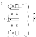
- Figure 3 depicts a peripheral area 300 of a device in which a number of regions are disposed and configured for partial biasing of a buried isolation barrier. For ease in illustration, the regions are shown after performance of implants but before any significant thermal diffusion.
- Formed in the peripheral area 300 are a depleted well region 302 and a depleted edge well region 304.
- the regions 302, 304 have a lateral profile that differs from the examples described above in connection with Figures 1 and 2 .
- n-type dopant is implanted in areas spaced from the surrounding regions of the doped isolation barriers. Specifically, a spacing 306 exists between the depleted well region 302 and an isolation well 310, and a spacing 308 exists between the depleted edge well region 304 and an edge isolation well 312.
- the location of the spacings 306, 308 may help deplete the well regions 302, 304 after thermal diffusion spreads the n-type dopant throughout the spacings 306, 308.
- the spacings 306, 308 are laterally farther away from the p-type dopant in a central gap 314.
- the portion or section of the depleted well regions 302, 304 having a lower dopant concentration level is farthest away from the p-type doped region in the central gap 314.
- the depletion of those sections of the well regions 302, 304 may thus be achieved more easily than if, for instance, gaps in the implant areas were positioned as described above in connection with Figures 1 and 2 .
- any misalignment of the n-type and p-type implants used to form the regions 302, 304 and p-type regions 314, 316 relative to the position of an isolation contact region 318 (via, e.g., the formation of STI regions) may change the extent to which the dopant concentration level is lowered near the isolation wells 310, 312. For instance, misalignment resulting in a leftward shift of the n-type and p-type implants may render it more difficult to sufficiently deplete the well region 302 near the isolation well 310.
- Figures 1-3 may schematically depict an Ohmic metal layer and metal-one layer used to form various electrodes, Figures 1-3 do not show a number of other metal layers configured for interconnections with the electrodes.
- the devices may have a number of other structures or components for connectivity, isolation, passivation, and other purposes not shown in Figures 1-3 for ease in illustration. For instance, the devices may include a number of additional backside layers.
- the dopant concentrations, thicknesses, and other characteristics of the above-described semiconductor regions in the semiconductor substrate 22 may vary.
- the above-referenced semiconductor regions may have the following approximate concentrations and thicknesses: Concentration Thickness p-epi 24: 1x10 13 - 5x10 15 /cm 3 3-10 ⁇ m substrate 26: 1x10 15 - 1x10 18 /cm 3 not applicable buried layer 30: 1x10 13 - 1x10 16 /cm 3 0.5-2 ⁇ m wells 32, 36: 1x10 12 - 1x10 15 /cm 3 1-2.5 ⁇ m wells 34, 37: 1x10 12 - 1x10 15 /cm 3 1-2.5 ⁇ m body 48: 1x10 16 - 1x10 18 /cm 3 0.5 - 1.5 ⁇ m source 44: 1x10 21 - 5x10 21 /cm 3 0.15 - 0.25 ⁇ m drain 46: 1x10 21 - 5
- concentrations and thicknesses may be different in other embodiments.
- the dopant concentration of the bulk substrate 26 may vary considerably.
- Figure 4 shows an exemplary method 400 for fabricating one or more of the above-described devices.
- the method 400 is configured to fabricate both a p-channel device and an n-channel device.
- One or both of the devices may be LDMOS devices having a RESURF configuration and one or more of the above-described features directed to partially biasing a doped isolation barrier.
- the devices are fabricated with a p-type bulk semiconductor substrate, the regions or layers of which may have the conductivity types of the n-channel and p-channel examples described above, or be alternatively fabricated with an n-type substrate.
- the method includes a sequence of acts, only the salient of which are depicted for convenience in illustration.
- an act directed to forming isolation wells may be implemented after one or more acts configured to form well regions that are depleted to support partial biasing of a doped isolation barrier.
- the method 400 may begin with one or more acts directed to the growth or other formation of one or more epitaxial layers.
- a p-type epitaxial layer is grown on a p-type bulk substrate in an act 402.
- the act 402 may be optional, e.g., in the interest of reducing process costs.
- an isolation layer is formed in an act 404.
- the act 404 may include a dopant implantation or other doping technique. In other cases, the isolation layer is formed before the growth of an epitaxial layer.
- the method 400 then includes growth (e.g., further growth) of a p-type epitaxial layer in an act 406.
- the isolation layer becomes a buried isolation layer.
- the isolation layer may be configured with a gap outside a core device area, as described above.
- the act 404 may include implementation of a photolithographic or other patterning procedure.
- STI regions and DTI structures are formed in an act 408.
- the STI regions may be used to define and separate active areas within and outside of the core device area.
- One or more STI regions may also be used to space a drain region from a gate structure in a field drift arrangement, as described above.
- the DTI structures may be ring-shaped to define a device area for each device.
- the act 408 is implemented after implementation of one or more the implant procedures described below.
- the STI regions and DTI structures may be formed via any now known or hereafter developed procedure.
- the act 408 may include the formation of a trench and the deposition (e.g., chemical vapor deposition, or CVD) of one or more materials in the trench.
- the trench is filled with silicon oxide. Additional or alternative materials may be deposited.
- an implantation is performed to form a sidewall of a doped isolation barrier.
- the implantation may be configured to form one or more isolation wells, which may be vertically stacked upon one another to define the sidewall.
- the sidewall of the doped isolation barrier defines the lateral boundary of the core device area of the device.
- the isolation wells may be positioned to extend upward from the buried isolation layer such that doped isolation barrier is shaped as an isolation tub.
- the implantation of the act 410 may also form edge isolation wells along the DTI structure, as described above.
- the act 410 may be performed at various points in the fabrication procedure.
- One or more dopant implantations are performed in an act 412 to form a number of well regions of the n-channel and p-channel devices.
- Each implantation may be configured to form multiple well regions.
- the multiple well regions of each implantation are configured and positioned for different purposes, despite having a common dopant concentration profile, as described above.
- An n-type implantation of the act 412 is configured to form a drift region of the n-channel device and/or a body region of the p-channel device, as well as one or more depleted well regions of both the n-channel and p-channel devices.
- the depleted well regions are disposed outside of the core device area.
- the depleted well region(s) electrically couple the isolation contact region and the doped isolation barrier to support the partial biasing of the doped isolation barrier, as described above.
- the p-type implantation of the act 412 may be directed to forming the buried well regions used to deplete the depleted well regions, as well as a RESURF region of the n-channel device used to deplete the drift region, and a buried well region used to isolate the body region of the p-channel device within the core device area.
- the n-type and p-type implantations of the act 412 use the same mask, as noted in act 414.
- the n-type and p-type implantations of the act 412 may also include configuring the implantations in an act 416 such that the depleted well regions (and the buried well regions in contact therewith) have exterior and interior gaps, as described above.
- the exterior gap may be under an isolation contact region, while the interior gaps are positioned to define an interior portion of the depleted well regions with a lower dopant concentration level for easier depletion.
- the implantations are configured such that the depleted well regions and corresponding buried well regions do not extend across an entire lateral extent of the isolation contact region.
- the n-type and p-type implantations of the act 412 may be configured to provide dopant throughout a well area of the well regions except an interior portion of the well area.
- the act 412 may then include driving the dopant of the third implantation via thermal diffusion into the interior portion such that the well regions have a lower interior dopant concentration level for depletion of the well regions.
- a separate p-type implantation procedure is implemented in an act 418 to form the body region of the n-channel device.
- a p-type implantation procedure is implemented to form a drift region of the p-channel device.
- the p-type implantation may also be configured to form a buried well region directed to laterally isolating the body region of the p-channel device within the core device area. The order in which these implantation procedures are implemented may vary from the order shown in Figure 4 .
- the foregoing implantation procedures may be configured such that the body region of the p-channel device is electrically isolated from the doped isolation barrier within the core device area, and such that the doped isolation barrier is biased at a different voltage level than the isolation contact region, as described above.
- the fabrication process may then include one or more procedures collectively shown in act 422.
- the procedures may be implemented in various orders. Additional or alternative procedures may be implemented.
- One or more components of a gate structure may be initially be formed. For instance, a gate dielectric layer and conductive plate may be deposited and patterned. A number of implants may then be performed in an act 424 to form LDD regions. After the dopant for the LDD regions is implanted, sidewall spacers may then be deposited in an act 426. The sidewall spacers and/or other components of the gate structure may then be used for self-alignment of a source region.
- n-type and p-type source/drain implantations are performed to form the various n-type and p-type contact regions of the devices, respectively. Source and drain regions may thus be formed for both the n-channel and p-channel devices.
- the n-type source/drain implantation is also configured to form an isolation contact region outside of the core device area of the n-channel and p-channel devices.
- the p-type and n-type body contact regions of the n-channel and p-channel devices are also formed.
- a number of metal and passivation layers may then be deposited on the substrate in an act 432.
- the metal layers may be patterned to form Ohmic contacts and electrodes, as well as field plates as described above, and various interconnects, including interconnects to bias the isolation contact regions as described above.
- any number of epitaxial layers may be grown on the original, bulk substrate.
- a number of acts are optional, including, for instance, acts related to elements or aspects of a gate structure or the channel, such as the formation of sidewall spacers and LDD regions.
- the following steps are performed: 402 - grow p-type epitaxial layer; 404 form (buried) doped isolation layer with gap outside device cores, 406 - further grow p-type epitaxial layer, 408 - form isolation regions (STI/DTI regions), 410 - form doped isolation walls of isolation tub (and define device cores), 412 - perform drift region implants(s) and drive dopants to define NLDMOS resurf drift region, both depleted well regions of NLDMOS and PLDMOS devices, and core-isolated body of PLDMOS device, 414 - perform n-type and p-type implants using same mask, 416 - configure implants such that depleted well regions include exterior and interior gaps, 418 - implant p-type dopant to form well of NLDMOS body region, 420 - implant p-type dopant to perform drift region and outer body isolation well of PLDMOS device, 422 - form gate structures, 424 - perform
- the disclosed devices are not limited to any particular transistor configuration.
- the partial isolation biasing of the disclosed devices may be useful in a wide variety of power electronic devices. For instance, application of the features of the disclosed devices is not limited to LDMOS or other power MOS devices.
- the partial isolation biasing is also not limited to any one particular type of RESURF configuration.
- the disclosed devices may have varying RESURF structures, including single, double, or other RESURF structural arrangements, each of which may be referred to herein as a "RESURF transistor.”
- n-channel and p-channel LDMOS devices with a p-type substrate are described and illustrated.
- the disclosed devices are not limited to p-type substrates, such that other types of devices may be provided by, for example, substitution of semiconductor regions of opposite conductivity type.
- each semiconductor region, layer or other structure in the example described in connection with Figures 1 and 2 may have a conductivity type (e.g., n-type or p-type) opposite to the type identified in the examples below.
- a device in a first aspect, includes a device includes a semiconductor substrate, a doped isolation barrier disposed in the semiconductor substrate and defining a core device area within the doped isolation barrier, an isolation contact region disposed in the semiconductor substrate outside of the core device area and to which a voltage is applied during operation, and a depleted well region disposed in the semiconductor substrate outside of the core device area, the depleted well region electrically coupling the isolation contact region and the doped isolation barrier such that the doped isolation barrier is biased at a voltage level lower than the voltage applied to the isolation contact region.
- a device in a second aspect, includes a semiconductor substrate, a doped isolation barrier disposed in the semiconductor substrate and defining a core device area within the doped isolation barrier, source and drain regions disposed in the semiconductor substrate within the core device area, a body region disposed in the semiconductor substrate within the core device area, and in which the source region is disposed, a drift region disposed in the semiconductor substrate within the core device area, and in which the drain region is disposed, an isolation contact region disposed in the semiconductor substrate outside of the core device area and to which a voltage is applied during operation, and a depleted well region disposed in the semiconductor substrate outside of the core device area, the depleted well region coupling the isolation contact region and the doped isolation barrier such that the doped isolation barrier is biased at a voltage level lower than the voltage applied to the isolation contact region.
- the depleted well region has a dopant concentration profile in common with either the body region or the drift region.
- a device in a third aspect, includes a semiconductor substrate, a doped isolation barrier disposed in the semiconductor substrate and defining a core device area within the doped isolation barrier, an isolation contact region disposed in the semiconductor substrate outside of the core device area, and a body region disposed in the semiconductor substrate within the core device area, and in which a channel is formed during operation.
- the body region is electrically tied to the isolation contact region.
- the body region and the doped isolation barrier have a common conductivity type.
- the body region is electrically isolated from the doped isolation barrier within the core device area.
- the doped isolation barrier and the isolation contact region are not electrically tied to one another such that the doped isolation barrier is biased at a different voltage level than the isolation contact region.
- the present disclosure further extends to a device comprising: a semiconductor substrate; a doped isolation barrier disposed in the semiconductor substrate and defining a core device area within the doped isolation barrier; source and drain regions disposed in the semiconductor substrate within the core device area; a body region disposed in the semiconductor substrate within the core device area, and in which the source region is disposed; an isolation contact region disposed in the semiconductor substrate outside of the core device area and to which a voltage is applied during operation; and a depleted well region disposed in the semiconductor substrate outside of the core device area, the depleted well region coupling the isolation contact region and the doped isolation barrier such that the doped isolation barrier is biased at a voltage level lower than the voltage applied to the isolation contact region; wherein the depleted well region has a dopant concentration profile in common with the body region.
- a method of fabricating a transistor includes performing a first implantation to form a sidewall of a doped isolation barrier, the doped isolation barrier defining a core device area within the doped isolation barrier, performing a second implantation to form an isolation contact region outside of the core device area, and performing a third implantation to form a well region outside of the core device area, the well region electrically coupling the isolation contact region and the doped isolation barrier.
- the third implantation provides dopant throughout a well area of the well region except a portion of the well area.
- Performing the third implantation includes driving the dopant of the third implantation via diffusion into the portion such that the well region has a lower interior dopant concentration level for depletion of the well region between the doped isolation barrier and the isolation contact region.
- a method of fabricating a transistor includes performing a first implantation to form a sidewall of a doped isolation barrier, the doped isolation barrier defining a core device area within the doped isolation barrier, performing a second implantation to form an isolation contact region outside of the core device area, performing a third implantation to form a body region within the core device area, and depositing a metal layer to form an interconnect that electrically ties the body region to the isolation contact region.
- the first, second and third implantations are configured such that the body region and the doped isolation barrier have a common conductivity type, the body region is electrically isolated from the doped isolation barrier within the core device area, and the doped isolation barrier and the isolation contact region are not electrically tied to one another such that the doped isolation barrier is biased at a different voltage level than the isolation contact region.
- references to a well region or other doped region of a semiconductor having a certain conductivity type are intended to specify that the region has a net dopant concentration of the type indicated to support the indicated conductivity type.
- the region may have dopant of the other conductivity type therein, but the amount of such opposite dopant is insufficient to change the effective, or net, conductivity type of the region.
- MOS metal-oxide-semiconductor and the abbreviation "MOS” may be used even though such devices may not employ metals or oxides but various combinations of conductive materials, e.g., metals, alloys, silicides, doped semiconductors, etc., instead of simple metals, and insulating materials other than oxides (e.g., nitrides, oxy-nitride mixtures, etc.).
- MOS and LDMOS are intended to include such variations.
Abstract
Description
- The present embodiments relate to semiconductor devices.
- Integrated circuits (ICs) and other electronic devices often include arrangements of interconnected field effect transistors (FETs), also called metal-oxide-semiconductor (MOS) field effect transistors (MOSFETs), or simply MOS transistors or devices. A typical MOS transistor includes a gate electrode as a control electrode and spaced apart source and drain electrodes. A control voltage applied to the gate electrode controls the flow of current through a controllable conductive channel between the source and drain electrodes.
- Power transistor devices are designed to be tolerant of the high currents and voltages that are present in power applications such as motion control, air bag deployment, and automotive fuel injector drivers. One type of power MOS transistor is a laterally diffused metal-oxide-semiconductor (LDMOS) transistor. In an LDMOS device, a drift space is provided between the channel region and the drain region.
- LDMOS devices may be designed to operate in a high-side configuration in which all of the device terminals are level shifted with respect to the substrate potential. Devices configured for high-side operation have been applied in power switchers in DC-to-DC converters, which have respective LDMOS devices for the high side and low side. High-side capable devices are designed to prevent a direct forward bias or punch-through path from a body region of the LDMOS device to an underlying substrate.
- LDMOS devices are often used in applications, such as automotive applications, involving operational voltages greater than 40 volts. Breakdown resulting from applying such high voltages to the drain is often prevented through a reduced surface field (RESURF) structure in the LDMOS device design. The RESURF structure is designed to deplete the drift space of the LDMOS device in both vertical and lateral directions, thereby reducing the electric field near the surface at the drift region and thus raising the off-state breakdown voltage (BVdss) of the device.
- Some LDMOS devices have a "double RESURF" structure. For example, in n-channel LDMOS devices, the drift space contains an upper level n-type region and a lower level p-type region, with an n-type buried isolation layer beneath the p-type region. The double nature of the structure refers to the depletion of the two regions and the reduction of the electric field in the related junction areas. Double RESURF structures typically apply the drain voltage to isolation regions in order to deplete the both the n-type and p-type regions.
- However, biasing the isolation regions at the drain voltage increases the field stress between the body of the LDMOS device and a buried isolation layer. Breakdown may instead occur between the body and the buried isolation layer, thereby limiting the breakdown voltage. Previous efforts to address such source/body-based breakdown have introduced fabrication challenges or degraded the electrostatic discharge (ESD) and safe operating area (SOA) performance of the device.
- The components and the figures are not necessarily to scale, emphasis instead being placed upon illustrating the principles of the various embodiments. Moreover, in the figures, like reference numerals designate corresponding parts throughout the different views.
-
Figure 1 is a cross-sectional, schematic, partial view of an exemplary n-channel LDMOS (or NLDMOS) transistor with partially biased isolation in accordance with one embodiment. -
Figure 2 is a cross-sectional, schematic, partial view of an exemplary p-channel LDMOS (or PLDMOS) transistor with partially biased isolation and a core-isolated body in accordance with one embodiment. -
Figure 3 is a cross-sectional, schematic, partial view of a depleted well region for partially biased isolation in accordance with one embodiment. -
Figure 4 is a flow diagram of an exemplary fabrication sequence to construct NLDMOS and/or PLDMOS transistors having partially biased isolation in accordance with one embodiment. - Embodiments of laterally diffused metal oxide semiconductor (LDMOS) and other power transistor devices and electronic apparatus with partially biased isolation and/or core-isolated body regions are described. Isolation regions may be partially lifted to a bias voltage level using a well region that couples the isolation regions to an isolation contact region. The well region is positioned and otherwise configured to be depleted of charge carriers. As a result, some of the bias voltage applied to the isolation contact region is sustained across the depleted well region. Only a portion of the bias voltage is therefore passed on to the isolation regions. The depleted well region thus provides partial biasing, or lifting of the isolation potential.
- The partial lifting of the isolation potential avoids biasing the isolation regions at voltage levels that would otherwise establish the breakdown voltage level of the device. With significantly less voltage stress between the device body and the isolation regions, breakdown voltage levels (e.g., BVDSS levels) up to, for instance, 100 Volts or beyond may be achieved.
- The depleted well region is incorporated into a periphery of the device, rather than in the core device area. The peripheral location may be useful because, for large power devices, the size of the peripheral areas of the devices is relatively negligible. As a result, the overall increase in device size is negligible. Performance parameters related to device size, such as resistance, are thus not significantly affected.
- Another depleted well region may be used to partially bias isolation regions adjacent a deep trench isolation (DTI) region. Additional breakdown protection for the DTI region may thus be provided. In some cases, the depleted well regions are disposed in a laterally symmetrical arrangement about the isolation contact region, in which case the same amount of bias voltage is sustained. In other cases, the depleted well region protecting the DTI region may be larger (e.g., wider) such that even less voltage stress is placed on the DTI region.
- The depleted well region may be formed in both n-channel and p-channel devices. The method embodiments may form the depleted well region using an implant directed to forming a drift region (e.g., n-channel devices with a p-type substrate) or a body region (e.g., p-channel devices with a p-type substrate). Other regions may also be formed using available implants. For instance, a buried well region used to deplete the depleted well region may be configured to form a RESURF region used to deplete a drift region of an n-channel LDMOS device. Increases in fabrication costs may thus be avoided.
- In some embodiments, one or more aspects of the device in the core device area are configured to support the partial biasing of the isolation regions. For instance, in devices in which the device body and the isolation regions have the same conductivity type (e.g., p-channel devices with a p-type substrate), the device body may be electrically isolated from the isolation regions within the core device area. The device body may be surrounded by a number of oppositely doped, buried wells. One or more of the buried wells may be formed using an implant directed to forming other device regions, such as the implant that forms the buried well regions used to deplete both the depleted well region for partial isolation biasing and the drift region of, e.g., an n-channel LDMOS device with a p-type substrate.
-
Figure 1 is a schematic cross-sectional view of an example of anLDMOS device 20 constructed in accordance with one embodiment. In this embodiment, thedevice 20 is configured as an n-channel device. Thedevice 20 may be configured as a RESURF transistor. In this example, thedevice 20 has a double RESURF arrangement. - The
device 20 includes asemiconductor substrate 22, which may, in turn, include a number ofepitaxial layers 24. In this example, thesemiconductor substrate 22 includes a single p-typeepitaxial layer 24 grown on an original, bulk substrate 26. The original substrate 26 may be a heavily doped p-type substrate in some cases, such as those having multiple epitaxial layers. Thesubstrate 22 may be biased via asubstrate contact region 27. Thedevice 20 may alternatively or additionally include non-epitaxial layers in which one or more device regions are formed. - Any one or more of the layers of the
semiconductor substrate 22 may include silicon. Alternative or additional semiconductor materials may be used in other embodiments. The structural, material, and other characteristics of thesemiconductor substrate 22 may vary from the example shown. Although useful for increasing the breakdown voltage in connection with bulk substrates, the disclosed embodiments are not limited to bulk substrates. For example, thesemiconductor substrate 22 may be or include a silicon-on-insulator (SOI) substrate. Additional, fewer, or alternative layers may be included in thesemiconductor substrate 22. For example, any number of additional semiconductor and/or non-semiconductor layers may be included. The disclosed devices are thus not limited to, for instance, bulk silicon substrates or substrates including epitaxially grown layers, and instead may be supported by a wide variety of other types of semiconductor substrates. - A
device area 28 of thedevice 20 is depicted inFigure 1 . In this case, only one side or half of thedevice area 28 is shown. For example, thedevice area 28 may be laterally symmetrical about, e.g., a drain region, and, thus include a portion that mirrors the portion shown. Thedevice area 28 may be defined by one or more doped device isolating layers or other regions in the semiconductor substrate 22 (e.g., the epitaxial layer 24). The regions may be doped semiconductor regions and/or undoped (e.g., dielectric) regions. In this example, thedevice area 28 is defined by a deep-trench isolation (DTI)ring 29. The structures in thedevice area 28 are laterally isolated from a remainder of thesubstrate 22 by the deep-trench isolation (DTI)ring 29. - A doped isolation barrier is provided for further device isolation. The doped isolation barrier may be disposed along the periphery of the
device area 28. The doped isolation barrier may include a number of doped isolation layers and regions provided within theDTI ring 29 along the periphery of thedevice area 28. The layers and regions of the doped isolation barrier may laterally and/or otherwise surround the remainder of thedevice area 28 for further isolation of thedevice 20. For instance, the regions or layers of the doped isolation barrier may form an isolation tub in which the active components of thedevice 20 are disposed. The isolation tub includes a bottom and sidewalls extending upward from the bottom. In this example, the doped isolation barrier includes a buriedisolation layer 30 that defines a bottom of the isolation tub. The doped isolation barrier also includesisolation wells isolation wells isolation layer 30 to electrically connect the doped isolation barrier for thedevice 20. In other cases, a single well, or additional wells, may be used to define the sidewalls. In this example, with a p-type substrate, the regions and layers of the doped isolation barrier are n-type regions. - One or more of the doped isolation layers and regions may be replicated along the
DTI ring 29 to provide further isolation. In the example ofFigure 1 , regions 36-38 are formed along theDTI ring 29. Theregions isolation wells region 38 may be formed with, and configured similarly to, the buriedisolation layer 30. In some cases, the buriedisolation layer 30 has agap 40 that defines theregion 38. - The doped isolation barrier defines a
core device area 42 of thedevice 20. Thecore device area 42 may correspond with the area in which the active components of thedevice 20 are disposed. The buriedisolation layer 30 extends across the entire lateral extent of thecore device area 42. The lateral extent of thecore device area 42 is defined in this example by theisolation wells isolation wells core device area 42. - The buried
isolation layer 30 may be formed in thesemiconductor substrate 22 before the growth of theepitaxial layer 24 thereof. The buried n-type layer may thus extend laterally across and under the regions disposed, and later formed, in thecore device area 42. The buriedisolation layer 30 may alternatively or additionally assist in depletion of a drift region of thedevice 20 to support the RESURF effect, as described below. - One or more of the layers and regions of the doped isolation barrier may have a dopant concentration level and/or be otherwise configured for high voltage (HV) operation (e.g., high side operation in which the terminals of the
device 20 are level shifted relative to thesemiconductor substrate 22, which may be grounded). For example, the higher dopant concentration level of the isolation barrier layer may be useful in preventing punch-through. Any number of the device isolation wells, sinks, or buried layers may or may not be connected to one another. Additional, fewer, or alternative device isolation layers or regions may be provided in thesemiconductor substrate 22. - Within the
core device area 42, thedevice 20 includes asource region 44, adrain region 46, abody region 48 in which thesource region 44 is disposed, and adrift region 50 in which thedrain region 46 is disposed. In this example, thebody region 48 is a p-type well formed in theepitaxial layer 24 of thesubstrate 22. Thebody region 30 may be biased via one or more heavily doped p-type body contact regions orelectrodes 52 formed in or otherwise above the p-type well of thebody region 48 in thesemiconductor substrate 22. The dopant concentration of eachcontact region 52 may be at a level sufficient to establish an ohmic contact to thebody region 48. - The source and drain
regions Figure 1 . Any number of source or drainregions drain region 46 need not be centered or otherwise disposed between, or laterally surrounded by, thesource region 44 as shown. In this example, the source and drainregions epitaxial layer 24. The heavily doped n-type source region 44 is disposed within, on, and/or otherwise above thebody region 30. The heavily n-type dopeddrain region 46 is spaced from thebody region 48 along the lateral dimension shown inFigure 1 . Such spacing defines a conduction path of the device between the source and drainregions regions drain region 46 and thesource region 44. In this n-channel LDMOS configuration, thedrain region 46 is biased at a relatively high drain-source voltage, Vds, relative to thesource region 44. - The
device 20 includes one ormore gate structures 54 formed on or above asurface 56 of thesemiconductor substrate 22. In this example, thedevice 20 includes afield plate structure 58 over thedrift region 50 for depletion thereof. Thegate structure 54 is disposed between thesource region 44 and thedrain region 46. Thegate structure 54 and thefield plate structure 58 may be electrically connected to one another. In some embodiments, thegate structure 54 surrounds thedrain region 46, which may be centrally or internally disposed within thedevice area 28. Alternatively, thegate structure 54 may be arranged in a dual gate finger configuration in which two transistors are symmetrically arranged to share thesame drain region 46. Thegate structure 54 includes a polysilicon or other conductive plate located on or above a gate dielectric. For example, the gate dielectric may include silicon dioxide (or oxide) deposited or otherwise formed on thesurface 56. Thegate structure 54 may include one or moredielectric sidewall spacers 60 disposed along lateral edges of thegate structure 54. The sidewall spacers 60 may cover the lateral edges to act as a silicide blocker to prevent a silicide short along the surface of thesubstrate 22. In the example ofFigure 1 , adielectric structure 62 is disposed between thegate structure 54 and thefield plate 58. The sidewall spacers 60 may provide spacing to separate the conductive components of thegate structure 54 from thesource region 44 and other regions of thedevice region 28. In this example, one of thesidewall spacers 60 is used for alignment purposes in defining an edge of thesource region 44. - The configuration of the
gate structure 54 may vary. The configuration of thegate structure 54 may include multiple conductive layers (e.g., polysilicon plates). The components, materials, and other characteristics of thegate structure 54 may vary from the example shown. - A number of shallow trench isolation (STI) regions 64-66 may be formed at the
surface 56 in thesemiconductor substrate 22. In this embodiment, theSTI region 64 is disposed between thegate structure 54 and thedrain region 46 to protect thegate structure 54 from the high voltage applied to thedrain region 46. For example, theSTI region 64 may be configured to prevent or minimize hot carrier injection (HCI) into the oxide layer of thegate structure 54. TheSTI region 64 is disposed in thedrift region 50 to form a field drift structure. Theother STI regions core device area 42 and theoverall device area 28. TheSTI region 65 is disposed between thebody contact region 52 and anisolation contact region 68 outside of thecore device area 42. - Additional, fewer, or alternative STI regions may be disposed in the
semiconductor substrate 22 to isolate or separate various contact regions, as well as other regions within thedevice area 28 of thedevice 20. For example, thebody contact region 52 and thesource region 44 may be separated by an additional STI region. - The conduction path of the
device 20 may be configured with one or more lightly or intermediately doped transition regions 70 (e.g., n-type lightly doped drain, or NLDD, regions) at or near the source and drainregions transition region 70 may be or include a diffused region formed in connection with thesource region 44. Such transition regions may couple thesource region 44 to a channel region 72 (described below). In this example, thedevice 20 includes anNLDD region 70 adjacent thesource region 44. TheNLDD region 70 may extend laterally under thegate structure 54 as shown. - When the
gate structure 54 is biased, charge carriers (in this case, electrons; alternatively, holes) accumulate in one or more channel areas or regions 72. Each channel region 48 (or a portion thereof) may be formed in thebody region 48 under thegate structure 54. In this example, the accumulation of electrons results in a charge inversion in the channel region 72 from the p-type of thebody region 48 to an n-type conduction layer or area near thesurface 56 of thesemiconductor substrate 22. Once a sufficient amount of the charge carriers accumulate in the conduction layer or area, charge carriers are capable of flowing from thesource region 44 toward thedrain region 46 through the channel region 72. - The channel region 72 may include other regions or areas in the
semiconductor substrate 22 in which charge inversion or accumulation occurs as a result of the bias applied to thegate structure 54. Charge carriers may also accumulate outside of or beyond thebody region 48. For example, charge carriers may accumulate in a region of theepitaxial layer 24 between thebody region 48 and thedrift region 50, as well as in an accumulation region or portion of thedrift region 50 near thesurface 56 under thegate structure 54. - After exiting the channel region 72, the charge carriers drift through the
drift region 50 to reach thedrain region 36. Thedrift region 50 electrically couples thedrain region 46 and the channel region 72. Thedrift region 50 may be configured to allow the charge carriers to drift under the electric field established by the drain-source voltage applied between thedrain region 46 and thesource region 44. In this example, thedrift region 50 is an n-type well that laterally extends under theSTI region 64 as a field drift region. - The
drift region 50 may be configured to be depleted to reduce the magnitude of the electric field in areas in and/or around thedrift region 50 via the reduced surface field (RESURF) effect to increase the voltage at which breakdown occurs along the conduction path of thedevice 20. In this example, thedrift region 50 is depleted both laterally and vertically. A junction forms between the n-type well of thedrift region 50 and the p-type epitaxial layer 24 and/or thebody region 48 to establish a lateral RESURF effect. The junction is reverse-biased as a result of the application of a drain voltage Vds between thesource region 44 and thedrain region 46. Thedrift region 50 is also depleted vertically by a p-type buriedwell region 74 disposed under thedrift region 46. - Further depletion in and around the
drift region 50 may be achieved via a double RESURF arrangement in which a voltage is applied to the buriedisolation layer 30 to reverse bias a junction along the buriedwell region 74. To that end, thedevice 20 includes an interconnect 76 (e.g., a patterned metal interconnect) supported by thesubstrate 22 to electrically tie thedrain region 46 to theisolation contact region 68. A voltage may be applied during operation to the buriedisolation layer 30 via the other regions of the doped isolation barrier, in this case, thestacked isolation wells isolation layer 30. - However, the buried isolation layer and other components of the doped isolation barrier are biased at a voltage level lower than the drain-source bias voltage (e.g., the voltage applied to the isolation contact region 68). The full drain-source bias voltage is not directly applied to the doped isolation barrier. Instead, the potential of the doped isolation barrier is instead partially lifted to the voltage level of the drain-source bias voltage to lower the voltage stress between the
body region 48 and the doped isolation barrier (e.g., the buried isolation layer 30). - Such partial biasing of the doped isolation barrier is provided by a
depleted well region 78 disposed in thesemiconductor substrate 22 outside of thecore device area 42. Thedepleted well region 78 electrically couples theisolation contact region 68 and the doped isolation barrier. A portion of the drain-source bias voltage is supported by the depletedwell region 78, such that only part of the bias voltage reaches the doped isolation barrier. The doped isolation barrier may thus be biased at a voltage level lower than the voltage applied to theisolation contact region 68. In this example, thedepleted well region 78 is an n-type well that extends between, and is in contact with, theisolation contact region 68 and the isolation well 32. In other embodiments, thedepleted well region 78 may be laterally adjacent to additional and/or alternative regions or layers of the doped isolation barrier. As described below, thedepleted well region 78 may be formed in conjunction with thedrift region 50, thereby using a pre-existing implant(s). - The extent of the voltage drop across the depleted
well region 78 may vary in accordance with the extent to which the depletedwell region 78 is depleted of charge carriers. Thedepleted well region 78 may be partially or fully depleted of charge carriers. The extent to which the depletedwell region 78 is depleted of charge carriers may be enhanced by one or more structures or other characteristics of the periphery of thedevice area 28. The extent of the depletion may be enhanced both laterally and/or vertically, examples of which are described below. - In the embodiment of
Figure 1 , the lateral depletion of the depletedwell region 78 is enhanced through one or more gaps in the dopant implantation area for thedepleted well region 78. The lateral extent of the depletedwell region 78 is shown both before and after thermal diffusion (e.g., one or more post-implant dopant drives). Before thermal diffusion, thedepleted well region 78 may have aninterior gap 80. Thermal diffusion of the dopant of the depletedwell region 78 may then fill in thegap 80, thereby lowering the dopant concentration level within an interior section or portion of the depletedwell region 78. As a result, thedepleted well region 78 may include an interior section that corresponds with the location of thegap 80 that has a lower dopant concentration level than a pair ofexterior sections isolation contact region 68 and the isolation well 32 of the doped isolation barrier, respectively. The lower dopant concentration level allows the interior section to be more easily depleted of charge carriers, despite being farther away from a reverse-biased junction. As a result, a greater amount or degree of depletion of the depletedwell region 78 may thus be achieved. - The location of the
gap 80 may vary. However, the interior location of thegap 80 in the example ofFigure 1 may be useful in connection with possible mask misalignment. The interior gap allows the masks for the implantation and the formation of theSTI region 65 to be misaligned, and still provide the full effect of thegap 80. An alternative embodiment is shown and described in connection withFigure 3 . - Further lateral depletion is provided at the outer edge of the depleted
well region 78. Thedepleted well region 78 does not extend across the full lateral extent of theisolation contact region 68. Thedepleted well region 78 laterally overlaps theisolation contact region 68 to establish the electrical coupling. However, in this example, agap 86 is provided to allow the p-type epitaxial layer 24 to deplete the depletedwell region 78 along the outer side thereof. - Depletion is accomplished in the vertical direction in the example of
Figure 1 through the presence of a p-type buriedwell region 88. The buriedwell region 88 is disposed under and in contact with thedepleted well region 78. Thedepleted well region 78 may be thus be depleted from below in a manner similar to the way in which thedrift region 50 is depleted by the buriedwell region 74. - Depletion in the vertical direction is also attained via a
conductive flap 90 supported by thesubstrate 22 and positioned over thedepleted well region 78. Theconductive flap 90 is biased during operation to deplete the depletedwell region 78. In this n-channel example, theconductive flap 90 may be grounded or otherwise biased at a low voltage level relative to the drain-source bias voltage. As a result, the charge carriers (in this case, electrons) are pushed away from thesurface 56 of thesubstrate 22, thereby depleting thedepleted well region 78 from above. Theconductive flap 90 may include a polysilicon plate, one or more metal layers, or another conductive structure. - The
conductive flap 90 may be spaced from thesurface 56 of thesubstrate 22 by one or more passivation layers 92. Any one or more dielectric materials may be used for the passivation layer(s) 92. - The formation of the above-described regions involved in the partial biasing of the doped isolation barrier may not increase the complexity or cost of fabricating the
device 20. For instance, and as described below in connection with the exemplary fabrication process shown inFigure 4 , the same implants (and corresponding mask layers) may be used to form the peripheral regions involved in the partial biasing. The same implant may be used to form the depletedwell region 78 and thedrift region 50. Thedepleted well region 78 may thus have a dopant concentration profile in common with thedrift region 50. The same implant may be used to form the buriedwell region 88 and the buriedwell region 74. The buried wellregions Figure 1 , the n-type and p-type implants used to form these regions may be configured with the same mask, insofar as the layout of the n-type and p-type regions may be the same. - The partial biasing technique may also be used in connection with the edge regions disposed along the periphery of the
device area 28 to protect theDTI region 29. In this example, the edge regions are theisolation wells layer 38. These edge regions are disposed along the inner edge of the ring-shapedDTI region 29 to act as a doped edge isolation barrier that protects against breakdown across theDTI region 29. The partial biasing of these edge regions may be used to avoid the high voltage stress that would otherwise occur if the edge regions were biased at the full drain-source bias voltage. To that end, thedevice 20 includes a depletededge well region 92 disposed in thesemiconductor substrate 22 outside of thecore device area 42. The depletededge well region 92 and thedepleted well region 78 may be configured similarly (e.g., exactly). The depletededge well region 92 electrically couples theisolation contact region 68 and the regions of the doped edge isolation barrier. As a result, the doped edge isolation barrier is biased at a lower voltage level than the voltage applied to theisolation contact region 68. - The partial biasing of the edge regions along the
DTI region 29 may be greater, less than, or equal to the partial biasing of the doped isolation barrier. In the example ofFigure 1 , thedepleted well region 78 and the depletededge well region 92 are laterally symmetrical about theisolation contact region 68. The same extent of depletion of the depletededge well region 92 may thus be attained laterally via the same gaps (as described above) and vertically through a buried edge wellregion 94 and a furtherconductive flap 96. The edge regions of the doped edge isolation barrier may thus be biased at the same level as the regions of the other doped isolation barrier. In other cases, the partial biasing may differ if, for instance, the depleted well regions are not symmetrical (e.g., one may be wider than the other) and/or further depletion is not attained via, for instance, a conductive flap. The voltage level of the doped isolation barriers may thus be adjusted independently of one another. - The partial biasing of the doped isolation barriers may also be supported by the absence of the buried isolation layer 30 (or layer 38) under the depleted well
regions Figure 1 , thegap 40 in the buriedisolation layer 30 is positioned such that the buriedisolation layer 30 does not extend under the depleted wellregions core device area 42. In this way, the biasing of the buriedisolation layer 30 occurs via the lateral path involving, for instance, thedepleted well region 78 and theisolation wells isolation contact region 68. -
Figure 1 depicts thedevice 20 in simplified form in the sense that only one side of thedevice 20 is shown. Thedevice 20 may include another side configured in a manner similar to the depicted side. For example, the other side of thedevice 20 may mirror or match the depicted side, such that thedevice 20 is symmetrical about thedrain region 46. Thedrain region 46 may thus be disposed in the center (or along a central line) of thedevice 20. The other side may thus include asecond source region 44 separated from thedrain region 46 by asecond gate structure 54. In some embodiments, thesecond source region 44 and thesecond gate structure 54 are contiguously formed with the corresponding regions of thedevice 20 described above via one or more connecting structures offset from the lateral cross-section shown inFigure 1 . For example, thegate structure 54 may be U-shaped or arch-shaped (e.g., a single lateral connection) or toroidal or looped (e.g., two lateral connections) when viewed from above. The shapes of the above-described regions of thedevice 20 may vary considerably from these examples. -
Figure 2 depicts an example of a p-channel LDMOS device 100 having partially biased isolation in accordance with one embodiment. Thedevice 100 is configured similarly in many respects to the n-channel examples described above in connection withFigure 1 . Unless noted otherwise, the structures, components, and other elements of thedevice 100 may be configured as described above in connection withFigure 1 . However, the differences between thedevices device 100. A number of differences instead arise from the use of a p-type substrate for thedevice 100. Indeed, in the example ofFigure 2 , thedevice 100 is formed in the same p-type substrate 22 in which thedevice 20 is formed. Thedevice 100 may present other differences not related to partial biasing, such as the configuration of a gate structure, and whether a field plate structure is included. - The use of the p-
type substrate 22 also leads to a number of other aspects in common with thedevice 20 ofFigure 1 . For instance, the isolation-related elements of thedevices Figure 1 . For example, thedevice 100 may include aDTI structure 29 that defines adevice area 28, a doped isolation barrier that includes a buriedisolation layer 30 andisolation wells DTI structure 29, such as edge regions 36-38. Each of the doped regions may be n-type regions as described above. - The elements of the
device 100 directed to partial biasing of the doped isolation barrier of thedevice 100 may also be configured as described above, including the conductivity type. Thus, thedevice 100 includes anisolation contact region 68, and depleted wellregion 78, depletededge well region 92, buried wellregions depleted well region 78 and the depletededge well region 92 allow the regions of the doped isolation barriers of thedevice 100 to be biased at a voltage level lower than the voltage applied to theisolation contact region 68, as described above. - The differences presented by the
device 100 involve the elements disposed in acore device area 42. In the p-channel example ofFigure 1 , the voltage applied to theisolation contact region 68 is the bias voltage applied to asource region 102 and abody region 104, rather than adrain region 106. Aninterconnect 108 is used to electrically tie theisolation contact region 68 to thesource region 102 and, via abody contact region 110, thebody region 104. The partial lifting effected by the depleted wellregions body region 104, rather than adrift region 112. In this case, the source and drainregions body contact region 110 is a heavily doped n-type region. Thesource region 102 is disposed in an n-type well of thebody region 104. As a result, thebody region 104 and the regions and layers of the doped isolation barrier have a common conductivity type, in this example. Thedrain region 106 is disposed in a p-type well of thedrift region 112. - To allow the depleted well
regions body region 104 is electrically isolated from the regions and layers of the doped isolation barrier within thecore device area 42. To that end, thedevice 100 includes a number of buriedwell regions semiconductor substrate 22 within thecore device area 42. The buried wellregions body region 104. The buriedwell region 114 is laterally adjacent to thebody region 104, and disposed between thebody region 104 and theisolation wells body region 104 in a lateral direction. The buriedwell region 116 is disposed under thebody region 104 between thebody region 104 and the buriedisolation layer 30 to electrically isolate thebody region 104 in a vertical direction. Each of the buried wellregions body region 104 as shown inFigure 2 . Alternatively, the buried wellregions 114 may be adjacent to, but spaced from, thebody region 104, such that the p-type doping of theepitaxial layer 24 is disposed therebetween. - In the embodiment of
Figure 2 , the depleted wellregions body region 104 may have a common dopant concentration profile. The n-type implant used to form thebody region 104 may also be used to form the depleted wellregions well region 116 may also be used to form the buried wellregions regions Figure 1 , additional implants or masks need not be added to the fabrication process to form the regions involved in the partial biasing of the doped isolation barrier. Also as described above in connection withFigure 1 , the same mask may be used to configure both of these n-type and p-type implants. As a result, the biasing of the doped isolation barrier may be achieved in a cost-effective manner. - The formation of the buried
well region 114 may also rely on a pre-existing implant procedure. In this example, the implant used to form thedrift region 112 may also form the buriedwell region 114. Thedrift region 112 and the buriedwell region 114 may thus have a common dopant concentration profile in such n-channel LDMOS devices. -
Figure 3 depicts aperipheral area 300 of a device in which a number of regions are disposed and configured for partial biasing of a buried isolation barrier. For ease in illustration, the regions are shown after performance of implants but before any significant thermal diffusion. Formed in theperipheral area 300 are adepleted well region 302 and a depletededge well region 304. Theregions Figures 1 and2 . In this example, n-type dopant is implanted in areas spaced from the surrounding regions of the doped isolation barriers. Specifically, aspacing 306 exists between thedepleted well region 302 and an isolation well 310, and aspacing 308 exists between the depletededge well region 304 and an edge isolation well 312. - The location of the
spacings well regions spacings spacings central gap 314. As a result, the portion or section of the depleted wellregions central gap 314. The depletion of those sections of thewell regions Figures 1 and2 . However, in this case, any misalignment of the n-type and p-type implants used to form theregions type regions isolation wells well region 302 near the isolation well 310. - The above-described devices are shown in simplified form. For example, while
Figures 1-3 may schematically depict an Ohmic metal layer and metal-one layer used to form various electrodes,Figures 1-3 do not show a number of other metal layers configured for interconnections with the electrodes. The devices may have a number of other structures or components for connectivity, isolation, passivation, and other purposes not shown inFigures 1-3 for ease in illustration. For instance, the devices may include a number of additional backside layers. - The dopant concentrations, thicknesses, and other characteristics of the above-described semiconductor regions in the
semiconductor substrate 22 may vary. In one example of the embodiment shown inFigure 1 , the above-referenced semiconductor regions may have the following approximate concentrations and thicknesses:Concentration Thickness p-epi 24: 1x10¹³ - 5x10¹⁵/cm3 3-10 µm substrate 26: 1x10¹⁵ - 1x10¹⁸/cm3 not applicable buried layer 30: 1x10¹³ - 1x10¹⁶/cm3 0.5-2 µm wells 32, 36: 1x10¹² - 1x10¹⁵/cm3 1-2.5 µm wells 34, 37: 1x10¹² - 1x10¹⁵/cm3 1-2.5 µm body 48: 1x10¹⁶ - 1x10¹⁸/cm3 0.5 - 1.5 µm source 44: 1x10²¹ - 5x10²¹/cm3 0.15 - 0.25 µm drain 46: 1x10²¹ - 5x10²¹/cm3 0.15 - 0.25 µm drift 50, 78: 5x10¹⁵ - 5x10¹⁷/cm3 0.5 - 1.5 µm iso contact 68: 1x10²¹ - 5x10²¹/cm3 0.15 - 0.25 µm NLDD 70: 1x10¹⁷ - 1x10¹⁹/cm3 0.2 - 0.3 µm buried 74, 88: 1x10¹² - 1x10¹⁵/cm3 1-2.5 µm - The concentrations and thicknesses may be different in other embodiments. For example, the dopant concentration of the bulk substrate 26 may vary considerably.
-
Figure 4 shows anexemplary method 400 for fabricating one or more of the above-described devices. In this example, themethod 400 is configured to fabricate both a p-channel device and an n-channel device. One or both of the devices may be LDMOS devices having a RESURF configuration and one or more of the above-described features directed to partially biasing a doped isolation barrier. The devices are fabricated with a p-type bulk semiconductor substrate, the regions or layers of which may have the conductivity types of the n-channel and p-channel examples described above, or be alternatively fabricated with an n-type substrate. The method includes a sequence of acts, only the salient of which are depicted for convenience in illustration. - The ordering of the acts may vary in other embodiments. For example, an act directed to forming isolation wells may be implemented after one or more acts configured to form well regions that are depleted to support partial biasing of a doped isolation barrier.
- The
method 400 may begin with one or more acts directed to the growth or other formation of one or more epitaxial layers. In this example, a p-type epitaxial layer is grown on a p-type bulk substrate in anact 402. In some cases, e.g., where the p-type bulk substrate is lightly doped, theact 402 may be optional, e.g., in the interest of reducing process costs. During or after the formation of the epitaxial layer, an isolation layer is formed in anact 404. Theact 404 may include a dopant implantation or other doping technique. In other cases, the isolation layer is formed before the growth of an epitaxial layer. In either case, themethod 400 then includes growth (e.g., further growth) of a p-type epitaxial layer in anact 406. As a result, the isolation layer becomes a buried isolation layer. The isolation layer may be configured with a gap outside a core device area, as described above. To that end, theact 404 may include implementation of a photolithographic or other patterning procedure. - In the example of
Figure 4 , a number of STI regions and DTI structures are formed in anact 408. The STI regions may be used to define and separate active areas within and outside of the core device area. One or more STI regions may also be used to space a drain region from a gate structure in a field drift arrangement, as described above. The DTI structures may be ring-shaped to define a device area for each device. In some cases, theact 408 is implemented after implementation of one or more the implant procedures described below. - The STI regions and DTI structures may be formed via any now known or hereafter developed procedure. In some cases, the
act 408 may include the formation of a trench and the deposition (e.g., chemical vapor deposition, or CVD) of one or more materials in the trench. In some embodiments, the trench is filled with silicon oxide. Additional or alternative materials may be deposited. - In an
act 410, an implantation is performed to form a sidewall of a doped isolation barrier. The implantation may be configured to form one or more isolation wells, which may be vertically stacked upon one another to define the sidewall. The sidewall of the doped isolation barrier defines the lateral boundary of the core device area of the device. The isolation wells may be positioned to extend upward from the buried isolation layer such that doped isolation barrier is shaped as an isolation tub. The implantation of theact 410 may also form edge isolation wells along the DTI structure, as described above. Theact 410 may be performed at various points in the fabrication procedure. - One or more dopant implantations are performed in an
act 412 to form a number of well regions of the n-channel and p-channel devices. Each implantation may be configured to form multiple well regions. The multiple well regions of each implantation are configured and positioned for different purposes, despite having a common dopant concentration profile, as described above. - An n-type implantation of the
act 412 is configured to form a drift region of the n-channel device and/or a body region of the p-channel device, as well as one or more depleted well regions of both the n-channel and p-channel devices. The depleted well regions are disposed outside of the core device area. The depleted well region(s) electrically couple the isolation contact region and the doped isolation barrier to support the partial biasing of the doped isolation barrier, as described above. - The p-type implantation of the
act 412 may be directed to forming the buried well regions used to deplete the depleted well regions, as well as a RESURF region of the n-channel device used to deplete the drift region, and a buried well region used to isolate the body region of the p-channel device within the core device area. - In some cases, the n-type and p-type implantations of the
act 412 use the same mask, as noted inact 414. The n-type and p-type implantations of theact 412 may also include configuring the implantations in anact 416 such that the depleted well regions (and the buried well regions in contact therewith) have exterior and interior gaps, as described above. The exterior gap may be under an isolation contact region, while the interior gaps are positioned to define an interior portion of the depleted well regions with a lower dopant concentration level for easier depletion. With the exterior gaps, the implantations are configured such that the depleted well regions and corresponding buried well regions do not extend across an entire lateral extent of the isolation contact region. With the interior gaps, the n-type and p-type implantations of theact 412 may be configured to provide dopant throughout a well area of the well regions except an interior portion of the well area. Theact 412 may then include driving the dopant of the third implantation via thermal diffusion into the interior portion such that the well regions have a lower interior dopant concentration level for depletion of the well regions. - In the example of
Figure 4 , a separate p-type implantation procedure is implemented in anact 418 to form the body region of the n-channel device. In anact 420, a p-type implantation procedure is implemented to form a drift region of the p-channel device. In some cases, the p-type implantation may also be configured to form a buried well region directed to laterally isolating the body region of the p-channel device within the core device area. The order in which these implantation procedures are implemented may vary from the order shown inFigure 4 . - Collectively, the foregoing implantation procedures may be configured such that the body region of the p-channel device is electrically isolated from the doped isolation barrier within the core device area, and such that the doped isolation barrier is biased at a different voltage level than the isolation contact region, as described above.
- The fabrication process may then include one or more procedures collectively shown in
act 422. The procedures may be implemented in various orders. Additional or alternative procedures may be implemented. One or more components of a gate structure may be initially be formed. For instance, a gate dielectric layer and conductive plate may be deposited and patterned. A number of implants may then be performed in anact 424 to form LDD regions. After the dopant for the LDD regions is implanted, sidewall spacers may then be deposited in anact 426. The sidewall spacers and/or other components of the gate structure may then be used for self-alignment of a source region. - In
acts - A number of metal and passivation layers may then be deposited on the substrate in an
act 432. The metal layers may be patterned to form Ohmic contacts and electrodes, as well as field plates as described above, and various interconnects, including interconnects to bias the isolation contact regions as described above. - Additional, fewer, or alternative acts may be implemented. For example, any number of epitaxial layers may be grown on the original, bulk substrate. A number of acts are optional, including, for instance, acts related to elements or aspects of a gate structure or the channel, such as the formation of sidewall spacers and LDD regions.
- In one or more embodiments, the following steps are performed: 402 - grow p-type epitaxial layer; 404 form (buried) doped isolation layer with gap outside device cores, 406 - further grow p-type epitaxial layer, 408 - form isolation regions (STI/DTI regions), 410 - form doped isolation walls of isolation tub (and define device cores), 412 - perform drift region implants(s) and drive dopants to define NLDMOS resurf drift region, both depleted well regions of NLDMOS and PLDMOS devices, and core-isolated body of PLDMOS device, 414 - perform n-type and p-type implants using same mask, 416 - configure implants such that depleted well regions include exterior and interior gaps, 418 - implant p-type dopant to form well of NLDMOS body region, 420 - implant p-type dopant to perform drift region and outer body isolation well of PLDMOS device, 422 - form gate structures, 424 - perform n-type and p-type LDD implants, 426 - deposit sidewall spacers, 428 - perform n-type source/drain implant and drive dopant to form n-type contact regions, 430 - perform p-type source/drain implant and drive dopant to perform p-type contact regions, 432 - deposit metal (e.g., for isolation contact connections) and passivation layers, as
figure 4 . - Although described in connection with respective n-channel and p-channel LDMOS transistors, the disclosed devices are not limited to any particular transistor configuration. The partial isolation biasing of the disclosed devices may be useful in a wide variety of power electronic devices. For instance, application of the features of the disclosed devices is not limited to LDMOS or other power MOS devices. The partial isolation biasing is also not limited to any one particular type of RESURF configuration. The disclosed devices may have varying RESURF structures, including single, double, or other RESURF structural arrangements, each of which may be referred to herein as a "RESURF transistor."
- For convenience of description and without any intended limitation, n-channel and p-channel LDMOS devices with a p-type substrate are described and illustrated. However, the disclosed devices are not limited to p-type substrates, such that other types of devices may be provided by, for example, substitution of semiconductor regions of opposite conductivity type. Thus, for example, each semiconductor region, layer or other structure in the example described in connection with
Figures 1 and2 may have a conductivity type (e.g., n-type or p-type) opposite to the type identified in the examples below. - In a first aspect, a device includes a device includes a semiconductor substrate, a doped isolation barrier disposed in the semiconductor substrate and defining a core device area within the doped isolation barrier, an isolation contact region disposed in the semiconductor substrate outside of the core device area and to which a voltage is applied during operation, and a depleted well region disposed in the semiconductor substrate outside of the core device area, the depleted well region electrically coupling the isolation contact region and the doped isolation barrier such that the doped isolation barrier is biased at a voltage level lower than the voltage applied to the isolation contact region.
- In a second aspect, a device includes a semiconductor substrate, a doped isolation barrier disposed in the semiconductor substrate and defining a core device area within the doped isolation barrier, source and drain regions disposed in the semiconductor substrate within the core device area, a body region disposed in the semiconductor substrate within the core device area, and in which the source region is disposed, a drift region disposed in the semiconductor substrate within the core device area, and in which the drain region is disposed, an isolation contact region disposed in the semiconductor substrate outside of the core device area and to which a voltage is applied during operation, and a depleted well region disposed in the semiconductor substrate outside of the core device area, the depleted well region coupling the isolation contact region and the doped isolation barrier such that the doped isolation barrier is biased at a voltage level lower than the voltage applied to the isolation contact region. The depleted well region has a dopant concentration profile in common with either the body region or the drift region.
- In a third aspect, a device includes a semiconductor substrate, a doped isolation barrier disposed in the semiconductor substrate and defining a core device area within the doped isolation barrier, an isolation contact region disposed in the semiconductor substrate outside of the core device area, and a body region disposed in the semiconductor substrate within the core device area, and in which a channel is formed during operation. The body region is electrically tied to the isolation contact region. The body region and the doped isolation barrier have a common conductivity type. The body region is electrically isolated from the doped isolation barrier within the core device area. The doped isolation barrier and the isolation contact region are not electrically tied to one another such that the doped isolation barrier is biased at a different voltage level than the isolation contact region.
- The present disclosure further extends to a device comprising: a semiconductor substrate; a doped isolation barrier disposed in the semiconductor substrate and defining a core device area within the doped isolation barrier; source and drain regions disposed in the semiconductor substrate within the core device area; a body region disposed in the semiconductor substrate within the core device area, and in which the source region is disposed; an isolation contact region disposed in the semiconductor substrate outside of the core device area and to which a voltage is applied during operation; and a depleted well region disposed in the semiconductor substrate outside of the core device area, the depleted well region coupling the isolation contact region and the doped isolation barrier such that the doped isolation barrier is biased at a voltage level lower than the voltage applied to the isolation contact region; wherein the depleted well region has a dopant concentration profile in common with the body region.
- In a fourth aspect, a method of fabricating a transistor includes performing a first implantation to form a sidewall of a doped isolation barrier, the doped isolation barrier defining a core device area within the doped isolation barrier, performing a second implantation to form an isolation contact region outside of the core device area, and performing a third implantation to form a well region outside of the core device area, the well region electrically coupling the isolation contact region and the doped isolation barrier. The third implantation provides dopant throughout a well area of the well region except a portion of the well area. Performing the third implantation includes driving the dopant of the third implantation via diffusion into the portion such that the well region has a lower interior dopant concentration level for depletion of the well region between the doped isolation barrier and the isolation contact region.
- In a fifth aspect, a method of fabricating a transistor includes performing a first implantation to form a sidewall of a doped isolation barrier, the doped isolation barrier defining a core device area within the doped isolation barrier, performing a second implantation to form an isolation contact region outside of the core device area, performing a third implantation to form a body region within the core device area, and depositing a metal layer to form an interconnect that electrically ties the body region to the isolation contact region. The first, second and third implantations are configured such that the body region and the doped isolation barrier have a common conductivity type, the body region is electrically isolated from the doped isolation barrier within the core device area, and the doped isolation barrier and the isolation contact region are not electrically tied to one another such that the doped isolation barrier is biased at a different voltage level than the isolation contact region.
- References to a well region or other doped region of a semiconductor having a certain conductivity type are intended to specify that the region has a net dopant concentration of the type indicated to support the indicated conductivity type. The region may have dopant of the other conductivity type therein, but the amount of such opposite dopant is insufficient to change the effective, or net, conductivity type of the region.
- Semiconductor devices with a conductive gate electrode positioned over a dielectric or other insulator may be considered MOS devices, despite the lack of a metal gate electrode and an oxide gate insulator. Accordingly, the terms metal-oxide-semiconductor and the abbreviation "MOS" may be used even though such devices may not employ metals or oxides but various combinations of conductive materials, e.g., metals, alloys, silicides, doped semiconductors, etc., instead of simple metals, and insulating materials other than oxides (e.g., nitrides, oxy-nitride mixtures, etc.). Thus, as used herein, the terms MOS and LDMOS are intended to include such variations.
- The present invention is defined by the following claims and their equivalents, and nothing in this section should be taken as a limitation on those claims. Further aspects and advantages of the invention are discussed above in conjunction with the preferred embodiments and may be later claimed independently or in combination.
- While the invention has been described above by reference to various embodiments, it should be understood that many changes and modifications may be made without departing from the scope of the invention. It is therefore intended that the foregoing detailed description be regarded as illustrative rather than limiting, and that it be understood that it is the following claims, including all equivalents, that are intended to define the spirit and scope of this invention.
Claims (15)
- A device comprising:a semiconductor substrate;a doped isolation barrier disposed in the semiconductor substrate and defining a core device area within the doped isolation barrier;an isolation contact region disposed in the semiconductor substrate outside of the core device area and to which a voltage is applied during operation; anda depleted well region disposed in the semiconductor substrate outside of the core device area, the depleted well region electrically coupling the isolation contact region and the doped isolation barrier such that the doped isolation barrier is biased at a voltage level lower than the voltage applied to the isolation contact region.
- The device of claim 1, further comprising a conductive flap supported by the semiconductor substrate and positioned over the depleted well region, the conductive flap being biased during operation to deplete the depleted well region.
- The device of claim 1 or 2, wherein:the depleted well region comprises a pair of exterior sections adjacent the isolation contact region and the doped isolation barrier, and an interior section disposed between the exterior sections; andthe interior section has a lower dopant concentration level than the pair of exterior sections.
- The device of any preceding claim, further comprising:a body region disposed in the semiconductor substrate within the core device area, having a first conductivity type, and in which a channel is formed during operation;a drift region disposed in the semiconductor substrate within the core device area, having a second conductivity type, and through which charge carriers drift during operation after exiting the channel;wherein the depleted well region has a dopant concentration profile in common with either the body region or the drift region.
- The device of any preceding claim, further comprising a buried well region disposed under and in contact with the depleted well region, wherein the buried well region has a first conductivity type and the depleted well region has a second conductivity type.
- The device of claim 5, further comprising:a body region disposed in the semiconductor substrate within the core device area, having a first conductivity type, and in which a channel is formed during operation;a drift region disposed in the semiconductor substrate within the core device area, having a second conductivity type, and through which charge carriers drift during operation after exiting the channel;a further buried well region disposed in the semiconductor substrate under and in contact with the drift region, having the first conductivity type, and configured to deplete the drift region;wherein the depleted well region and the drift region have a common dopant concentration profile; andwherein the buried well region and the further buried well region have a common dopant concentration profile.
- The device of any preceding claim, wherein the depleted well region does not extend across an entire lateral extent of the isolation contact region.
- The device of any preceding claim, further comprising:a deep trench isolation (DTI) region disposed in the semiconductor substrate, the DTI region being ring-shaped to surround the core device area;a doped edge isolation barrier disposed in the semiconductor substrate along the DTI region; anda depleted edge well region disposed in the semiconductor substrate outside of the core device area, the depleted edge well region electrically coupling the isolation contact region and the doped edge isolation barrier such that the doped edge isolation barrier is biased at a lower voltage level than the voltage applied to the isolation contact region.
- The device of claim 8, wherein the depleted well region and the depleted edge well region are laterally symmetrical about the isolation contact region.
- The device of any preceding claim, further comprising a drain region disposed in the semiconductor substrate within the core device area, wherein:the isolation contact region and the drain region are electrically tied to one another; andthe doped isolation barrier is not electrically tied to the drain region.
- The device of any preceding claim, wherein:the doped isolation barrier comprises a ring-shaped well region and a buried isolation layer extending from the ring-shaped well region under the device core area; and either (a) the buried isolation layer does not extend under the depleted well region outside of the core device area, or (b) the depleted well region is laterally adjacent and in contact with the ring-shaped well region.
- The device of any preceding claim, further comprising a body region disposed in the semiconductor substrate within the core device area, the body region having a first conductivity type, wherein the doped isolation barrier, the isolation contact region, and the depleted well region have a second conductivity type.
- A method of fabricating a transistor, the method comprising:performing a first implantation to form a sidewall of a doped isolation barrier, the doped isolation barrier defining a core device area within the doped isolation barrier;performing a second implantation to form an isolation contact region outside of the core device area; andperforming a third implantation to form a well region outside of the core device area, the well region electrically coupling the isolation contact region and the doped isolation barrier;wherein:the third implantation provides dopant throughout a well area of the well region except a portion of the well area;performing the third implantation comprises driving the dopant of the third implantation via diffusion into the portion such that the well region has a lower interior dopant concentration level for depletion of the well region between the doped isolation barrier and the isolation contact region.
- The method of claim 13, wherein the third implantation is configured either (a) such that the well region does not extend across an entire lateral extent of the isolation contact region, or (b) to form either a drift region of the transistor within the core device area or a body region of the transistor within the core device area.
- The method of claim 13 or 14, further comprising a fourth implantation to form a buried well region disposed under and in contact with the well region formed by the third implantation, wherein the buried well region has a first conductivity type and the depleted well region has a second conductivity type, and optionally the fourth implantation is further configured to form a further buried well region under either a drift region of the transistor within the core device area or a body region of the transistor within the core device area.
Applications Claiming Priority (1)
| Application Number | Priority Date | Filing Date | Title |
|---|---|---|---|
| US14/851,360 US10217860B2 (en) | 2015-09-11 | 2015-09-11 | Partially biased isolation in semiconductor devices |
Publications (2)
| Publication Number | Publication Date |
|---|---|
| EP3142150A1 true EP3142150A1 (en) | 2017-03-15 |
| EP3142150B1 EP3142150B1 (en) | 2020-02-12 |
Family
ID=56893826
Family Applications (1)
| Application Number | Title | Priority Date | Filing Date |
|---|---|---|---|
| EP16187929.1A Active EP3142150B1 (en) | 2015-09-11 | 2016-09-08 | Partially biased isolation in semiconductor devices |
Country Status (2)
| Country | Link |
|---|---|
| US (1) | US10217860B2 (en) |
| EP (1) | EP3142150B1 (en) |
Cited By (2)
| Publication number | Priority date | Publication date | Assignee | Title |
|---|---|---|---|---|
| CN107978632A (en) * | 2017-11-30 | 2018-05-01 | 电子科技大学 | The lateral high-voltage device of more raceway grooves |
| TWI808781B (en) * | 2022-06-08 | 2023-07-11 | 力晶積成電子製造股份有限公司 | Electrostatic discharge protection device |
Families Citing this family (3)
| Publication number | Priority date | Publication date | Assignee | Title |
|---|---|---|---|---|
| US9825169B2 (en) | 2015-12-16 | 2017-11-21 | Nxp Usa, Inc. | Partial, self-biased isolation in semiconductor devices |
| JP6591312B2 (en) * | 2016-02-25 | 2019-10-16 | ルネサスエレクトロニクス株式会社 | Semiconductor device |
| US9761707B1 (en) | 2016-08-19 | 2017-09-12 | Nxp Usa, Inc. | Laterally diffused MOSFET with isolation region |
Citations (4)
| Publication number | Priority date | Publication date | Assignee | Title |
|---|---|---|---|---|
| US20100038718A1 (en) * | 2008-08-13 | 2010-02-18 | Zhu Haiyang | Electro-static discharge and latchup resistant semiconductor device |
| US20110057262A1 (en) * | 2009-09-10 | 2011-03-10 | Episil Technologies Inc. | Semiconductor device |
| US20110241092A1 (en) * | 2010-03-30 | 2011-10-06 | Freescale Semiconductor, Inc. | Electronic device with capcitively coupled floating buried layer |
| US20130341730A1 (en) * | 2012-06-26 | 2013-12-26 | Infineon Technologies Ag | Semiconductor Devices and Structures |
Family Cites Families (20)
| Publication number | Priority date | Publication date | Assignee | Title |
|---|---|---|---|---|
| US4300150A (en) | 1980-06-16 | 1981-11-10 | North American Philips Corporation | Lateral double-diffused MOS transistor device |
| US6753575B2 (en) | 2002-06-11 | 2004-06-22 | Texas Instruments Incorporated | Tank-isolated-drain-extended power device |
| US7667268B2 (en) * | 2002-08-14 | 2010-02-23 | Advanced Analogic Technologies, Inc. | Isolated transistor |
| US6882023B2 (en) | 2002-10-31 | 2005-04-19 | Motorola, Inc. | Floating resurf LDMOSFET and method of manufacturing same |
| JP4800566B2 (en) | 2003-10-06 | 2011-10-26 | ルネサスエレクトロニクス株式会社 | Semiconductor device and manufacturing method thereof |
| US7608513B2 (en) * | 2007-01-25 | 2009-10-27 | Freescale Semiconductor, Inc. | Dual gate LDMOS device fabrication methods |
| US9484454B2 (en) | 2008-10-29 | 2016-11-01 | Tower Semiconductor Ltd. | Double-resurf LDMOS with drift and PSURF implants self-aligned to a stacked gate “bump” structure |
| KR101128694B1 (en) | 2009-11-17 | 2012-03-23 | 매그나칩 반도체 유한회사 | Semiconductor device |
| US8344472B2 (en) | 2010-03-30 | 2013-01-01 | Freescale Semiconductor, Inc. | Semiconductor device and method |
| US8541862B2 (en) * | 2011-11-30 | 2013-09-24 | Freescale Semiconductor, Inc. | Semiconductor device with self-biased isolation |
| KR101864889B1 (en) | 2012-01-20 | 2018-06-05 | 에스케이하이닉스 시스템아이씨 주식회사 | Lateral DMOS transistor and method of fabricating the same |
| KR101986090B1 (en) * | 2012-04-06 | 2019-06-05 | 삼성전자 주식회사 | Semiconductor device using guardring and semiconductor system comprising the same |
| US9236472B2 (en) * | 2012-04-17 | 2016-01-12 | Freescale Semiconductor, Inc. | Semiconductor device with integrated breakdown protection |
| US20130270636A1 (en) | 2012-04-17 | 2013-10-17 | Broadcom Corporation | Transistor Having An Isolated Body For High Voltage Operation |
| KR101988425B1 (en) * | 2012-11-05 | 2019-06-12 | 삼성전자주식회사 | Semiconductor Device and method for fabricating the same |
| KR20150028602A (en) * | 2013-09-06 | 2015-03-16 | 에스케이하이닉스 주식회사 | Semiconductor device and method for fabricating the same |
| US9660074B2 (en) * | 2014-08-07 | 2017-05-23 | Texas Instruments Incorporated | Methods and apparatus for LDMOS devices with cascaded RESURF implants and double buffers |
| US9306060B1 (en) | 2014-11-20 | 2016-04-05 | Freescale Semiconductor Inc. | Semiconductor devices and related fabrication methods |
| US9508845B1 (en) | 2015-08-10 | 2016-11-29 | Freescale Semiconductor, Inc. | LDMOS device with high-potential-biased isolation ring |
| US9728600B2 (en) * | 2015-09-11 | 2017-08-08 | Nxp Usa, Inc. | Partially biased isolation in semiconductor devices |
-
2015
- 2015-09-11 US US14/851,360 patent/US10217860B2/en active Active
-
2016
- 2016-09-08 EP EP16187929.1A patent/EP3142150B1/en active Active
Patent Citations (4)
| Publication number | Priority date | Publication date | Assignee | Title |
|---|---|---|---|---|
| US20100038718A1 (en) * | 2008-08-13 | 2010-02-18 | Zhu Haiyang | Electro-static discharge and latchup resistant semiconductor device |
| US20110057262A1 (en) * | 2009-09-10 | 2011-03-10 | Episil Technologies Inc. | Semiconductor device |
| US20110241092A1 (en) * | 2010-03-30 | 2011-10-06 | Freescale Semiconductor, Inc. | Electronic device with capcitively coupled floating buried layer |
| US20130341730A1 (en) * | 2012-06-26 | 2013-12-26 | Infineon Technologies Ag | Semiconductor Devices and Structures |
Cited By (3)
| Publication number | Priority date | Publication date | Assignee | Title |
|---|---|---|---|---|
| CN107978632A (en) * | 2017-11-30 | 2018-05-01 | 电子科技大学 | The lateral high-voltage device of more raceway grooves |
| CN107978632B (en) * | 2017-11-30 | 2020-06-16 | 电子科技大学 | Multi-channel transverse high-voltage device |
| TWI808781B (en) * | 2022-06-08 | 2023-07-11 | 力晶積成電子製造股份有限公司 | Electrostatic discharge protection device |
Also Published As
| Publication number | Publication date |
|---|---|
| EP3142150B1 (en) | 2020-02-12 |
| US10217860B2 (en) | 2019-02-26 |
| US20170077295A1 (en) | 2017-03-16 |
Similar Documents
| Publication | Publication Date | Title |
|---|---|---|
| US9680011B2 (en) | Self-adjusted isolation bias in semiconductor devices | |
| US9818863B2 (en) | Integrated breakdown protection | |
| US8541862B2 (en) | Semiconductor device with self-biased isolation | |
| US9640635B2 (en) | Reliability in mergeable semiconductor devices | |
| US10297676B2 (en) | Partially biased isolation in semiconductor device | |
| US9136323B2 (en) | Drain-end drift diminution in semiconductor devices | |
| US9543379B2 (en) | Semiconductor device with peripheral breakdown protection | |
| US9825169B2 (en) | Partial, self-biased isolation in semiconductor devices | |
| US9159803B2 (en) | Semiconductor device with HCI protection region | |
| US9024380B2 (en) | Semiconductor device with floating RESURF region | |
| US9673188B2 (en) | Integrated electrostatic discharge (ESD) clamping for an LDMOS transistor device having a bipolar transistor | |
| US9728600B2 (en) | Partially biased isolation in semiconductor devices | |
| EP3142150B1 (en) | Partially biased isolation in semiconductor devices | |
| US10177252B2 (en) | Semiconductor device isolation with RESURF layer arrangement | |
| US9761707B1 (en) | Laterally diffused MOSFET with isolation region | |
| US10032904B2 (en) | Semiconductor device with non-isolated power transistor with integrated diode protection | |
| US9941350B1 (en) | Semiconductor device isolation via depleted coupling layer | |
| US9614074B1 (en) | Partial, self-biased isolation in semiconductor devices | |
| US9831338B1 (en) | Alternating source region arrangement |
Legal Events
| Date | Code | Title | Description |
|---|---|---|---|
| PUAI | Public reference made under article 153(3) epc to a published international application that has entered the european phase |
Free format text: ORIGINAL CODE: 0009012 |
|
| STAA | Information on the status of an ep patent application or granted ep patent |
Free format text: STATUS: THE APPLICATION HAS BEEN PUBLISHED |
|
| AK | Designated contracting states |
Kind code of ref document: A1 Designated state(s): AL AT BE BG CH CY CZ DE DK EE ES FI FR GB GR HR HU IE IS IT LI LT LU LV MC MK MT NL NO PL PT RO RS SE SI SK SM TR |
|
| AX | Request for extension of the european patent |
Extension state: BA ME |
|
| STAA | Information on the status of an ep patent application or granted ep patent |
Free format text: STATUS: REQUEST FOR EXAMINATION WAS MADE |
|
| 17P | Request for examination filed |
Effective date: 20170915 |
|
| RBV | Designated contracting states (corrected) |
Designated state(s): AL AT BE BG CH CY CZ DE DK EE ES FI FR GB GR HR HU IE IS IT LI LT LU LV MC MK MT NL NO PL PT RO RS SE SI SK SM TR |
|
| GRAP | Despatch of communication of intention to grant a patent |
Free format text: ORIGINAL CODE: EPIDOSNIGR1 |
|
| STAA | Information on the status of an ep patent application or granted ep patent |
Free format text: STATUS: GRANT OF PATENT IS INTENDED |
|
| INTG | Intention to grant announced |
Effective date: 20191111 |
|
| GRAS | Grant fee paid |
Free format text: ORIGINAL CODE: EPIDOSNIGR3 |
|
| GRAA | (expected) grant |
Free format text: ORIGINAL CODE: 0009210 |
|
| STAA | Information on the status of an ep patent application or granted ep patent |
Free format text: STATUS: THE PATENT HAS BEEN GRANTED |
|
| AK | Designated contracting states |
Kind code of ref document: B1 Designated state(s): AL AT BE BG CH CY CZ DE DK EE ES FI FR GB GR HR HU IE IS IT LI LT LU LV MC MK MT NL NO PL PT RO RS SE SI SK SM TR |
|
| REG | Reference to a national code |
Ref country code: GB Ref legal event code: FG4D |
|
| REG | Reference to a national code |
Ref country code: CH Ref legal event code: EP |
|
| REG | Reference to a national code |
Ref country code: AT Ref legal event code: REF Ref document number: 1233237 Country of ref document: AT Kind code of ref document: T Effective date: 20200215 |
|
| REG | Reference to a national code |
Ref country code: IE Ref legal event code: FG4D |
|
| REG | Reference to a national code |
Ref country code: DE Ref legal event code: R096 Ref document number: 602016029413 Country of ref document: DE |
|
| PG25 | Lapsed in a contracting state [announced via postgrant information from national office to epo] |
Ref country code: FI Free format text: LAPSE BECAUSE OF FAILURE TO SUBMIT A TRANSLATION OF THE DESCRIPTION OR TO PAY THE FEE WITHIN THE PRESCRIBED TIME-LIMIT Effective date: 20200212 Ref country code: NO Free format text: LAPSE BECAUSE OF FAILURE TO SUBMIT A TRANSLATION OF THE DESCRIPTION OR TO PAY THE FEE WITHIN THE PRESCRIBED TIME-LIMIT Effective date: 20200512 Ref country code: RS Free format text: LAPSE BECAUSE OF FAILURE TO SUBMIT A TRANSLATION OF THE DESCRIPTION OR TO PAY THE FEE WITHIN THE PRESCRIBED TIME-LIMIT Effective date: 20200212 |
|
| REG | Reference to a national code |
Ref country code: LT Ref legal event code: MG4D |
|
| REG | Reference to a national code |
Ref country code: NL Ref legal event code: MP Effective date: 20200212 |
|
| PG25 | Lapsed in a contracting state [announced via postgrant information from national office to epo] |
Ref country code: GR Free format text: LAPSE BECAUSE OF FAILURE TO SUBMIT A TRANSLATION OF THE DESCRIPTION OR TO PAY THE FEE WITHIN THE PRESCRIBED TIME-LIMIT Effective date: 20200513 Ref country code: BG Free format text: LAPSE BECAUSE OF FAILURE TO SUBMIT A TRANSLATION OF THE DESCRIPTION OR TO PAY THE FEE WITHIN THE PRESCRIBED TIME-LIMIT Effective date: 20200512 Ref country code: HR Free format text: LAPSE BECAUSE OF FAILURE TO SUBMIT A TRANSLATION OF THE DESCRIPTION OR TO PAY THE FEE WITHIN THE PRESCRIBED TIME-LIMIT Effective date: 20200212 Ref country code: IS Free format text: LAPSE BECAUSE OF FAILURE TO SUBMIT A TRANSLATION OF THE DESCRIPTION OR TO PAY THE FEE WITHIN THE PRESCRIBED TIME-LIMIT Effective date: 20200612 Ref country code: LV Free format text: LAPSE BECAUSE OF FAILURE TO SUBMIT A TRANSLATION OF THE DESCRIPTION OR TO PAY THE FEE WITHIN THE PRESCRIBED TIME-LIMIT Effective date: 20200212 Ref country code: SE Free format text: LAPSE BECAUSE OF FAILURE TO SUBMIT A TRANSLATION OF THE DESCRIPTION OR TO PAY THE FEE WITHIN THE PRESCRIBED TIME-LIMIT Effective date: 20200212 |
|
| PG25 | Lapsed in a contracting state [announced via postgrant information from national office to epo] |
Ref country code: NL Free format text: LAPSE BECAUSE OF FAILURE TO SUBMIT A TRANSLATION OF THE DESCRIPTION OR TO PAY THE FEE WITHIN THE PRESCRIBED TIME-LIMIT Effective date: 20200212 |
|
| PG25 | Lapsed in a contracting state [announced via postgrant information from national office to epo] |
Ref country code: CZ Free format text: LAPSE BECAUSE OF FAILURE TO SUBMIT A TRANSLATION OF THE DESCRIPTION OR TO PAY THE FEE WITHIN THE PRESCRIBED TIME-LIMIT Effective date: 20200212 Ref country code: ES Free format text: LAPSE BECAUSE OF FAILURE TO SUBMIT A TRANSLATION OF THE DESCRIPTION OR TO PAY THE FEE WITHIN THE PRESCRIBED TIME-LIMIT Effective date: 20200212 Ref country code: RO Free format text: LAPSE BECAUSE OF FAILURE TO SUBMIT A TRANSLATION OF THE DESCRIPTION OR TO PAY THE FEE WITHIN THE PRESCRIBED TIME-LIMIT Effective date: 20200212 Ref country code: DK Free format text: LAPSE BECAUSE OF FAILURE TO SUBMIT A TRANSLATION OF THE DESCRIPTION OR TO PAY THE FEE WITHIN THE PRESCRIBED TIME-LIMIT Effective date: 20200212 Ref country code: SM Free format text: LAPSE BECAUSE OF FAILURE TO SUBMIT A TRANSLATION OF THE DESCRIPTION OR TO PAY THE FEE WITHIN THE PRESCRIBED TIME-LIMIT Effective date: 20200212 Ref country code: EE Free format text: LAPSE BECAUSE OF FAILURE TO SUBMIT A TRANSLATION OF THE DESCRIPTION OR TO PAY THE FEE WITHIN THE PRESCRIBED TIME-LIMIT Effective date: 20200212 Ref country code: LT Free format text: LAPSE BECAUSE OF FAILURE TO SUBMIT A TRANSLATION OF THE DESCRIPTION OR TO PAY THE FEE WITHIN THE PRESCRIBED TIME-LIMIT Effective date: 20200212 Ref country code: SK Free format text: LAPSE BECAUSE OF FAILURE TO SUBMIT A TRANSLATION OF THE DESCRIPTION OR TO PAY THE FEE WITHIN THE PRESCRIBED TIME-LIMIT Effective date: 20200212 Ref country code: PT Free format text: LAPSE BECAUSE OF FAILURE TO SUBMIT A TRANSLATION OF THE DESCRIPTION OR TO PAY THE FEE WITHIN THE PRESCRIBED TIME-LIMIT Effective date: 20200705 |
|
| REG | Reference to a national code |
Ref country code: DE Ref legal event code: R097 Ref document number: 602016029413 Country of ref document: DE |
|
| REG | Reference to a national code |
Ref country code: AT Ref legal event code: MK05 Ref document number: 1233237 Country of ref document: AT Kind code of ref document: T Effective date: 20200212 |
|
| PLBE | No opposition filed within time limit |
Free format text: ORIGINAL CODE: 0009261 |
|
| STAA | Information on the status of an ep patent application or granted ep patent |
Free format text: STATUS: NO OPPOSITION FILED WITHIN TIME LIMIT |
|
| 26N | No opposition filed |
Effective date: 20201113 |
|
| PG25 | Lapsed in a contracting state [announced via postgrant information from national office to epo] |
Ref country code: IT Free format text: LAPSE BECAUSE OF FAILURE TO SUBMIT A TRANSLATION OF THE DESCRIPTION OR TO PAY THE FEE WITHIN THE PRESCRIBED TIME-LIMIT Effective date: 20200212 Ref country code: AT Free format text: LAPSE BECAUSE OF FAILURE TO SUBMIT A TRANSLATION OF THE DESCRIPTION OR TO PAY THE FEE WITHIN THE PRESCRIBED TIME-LIMIT Effective date: 20200212 |
|
| PG25 | Lapsed in a contracting state [announced via postgrant information from national office to epo] |
Ref country code: PL Free format text: LAPSE BECAUSE OF FAILURE TO SUBMIT A TRANSLATION OF THE DESCRIPTION OR TO PAY THE FEE WITHIN THE PRESCRIBED TIME-LIMIT Effective date: 20200212 Ref country code: SI Free format text: LAPSE BECAUSE OF FAILURE TO SUBMIT A TRANSLATION OF THE DESCRIPTION OR TO PAY THE FEE WITHIN THE PRESCRIBED TIME-LIMIT Effective date: 20200212 |
|
| PG25 | Lapsed in a contracting state [announced via postgrant information from national office to epo] |
Ref country code: MC Free format text: LAPSE BECAUSE OF FAILURE TO SUBMIT A TRANSLATION OF THE DESCRIPTION OR TO PAY THE FEE WITHIN THE PRESCRIBED TIME-LIMIT Effective date: 20200212 |
|
| REG | Reference to a national code |
Ref country code: CH Ref legal event code: PL |
|
| GBPC | Gb: european patent ceased through non-payment of renewal fee |
Effective date: 20200908 |
|
| REG | Reference to a national code |
Ref country code: BE Ref legal event code: MM Effective date: 20200930 |
|
| PG25 | Lapsed in a contracting state [announced via postgrant information from national office to epo] |
Ref country code: LU Free format text: LAPSE BECAUSE OF NON-PAYMENT OF DUE FEES Effective date: 20200908 |
|
| PG25 | Lapsed in a contracting state [announced via postgrant information from national office to epo] |
Ref country code: FR Free format text: LAPSE BECAUSE OF NON-PAYMENT OF DUE FEES Effective date: 20200930 |
|
| PG25 | Lapsed in a contracting state [announced via postgrant information from national office to epo] |
Ref country code: BE Free format text: LAPSE BECAUSE OF NON-PAYMENT OF DUE FEES Effective date: 20200930 Ref country code: CH Free format text: LAPSE BECAUSE OF NON-PAYMENT OF DUE FEES Effective date: 20200930 Ref country code: GB Free format text: LAPSE BECAUSE OF NON-PAYMENT OF DUE FEES Effective date: 20200908 Ref country code: IE Free format text: LAPSE BECAUSE OF NON-PAYMENT OF DUE FEES Effective date: 20200908 Ref country code: LI Free format text: LAPSE BECAUSE OF NON-PAYMENT OF DUE FEES Effective date: 20200930 |
|
| PG25 | Lapsed in a contracting state [announced via postgrant information from national office to epo] |
Ref country code: TR Free format text: LAPSE BECAUSE OF FAILURE TO SUBMIT A TRANSLATION OF THE DESCRIPTION OR TO PAY THE FEE WITHIN THE PRESCRIBED TIME-LIMIT Effective date: 20200212 Ref country code: MT Free format text: LAPSE BECAUSE OF FAILURE TO SUBMIT A TRANSLATION OF THE DESCRIPTION OR TO PAY THE FEE WITHIN THE PRESCRIBED TIME-LIMIT Effective date: 20200212 Ref country code: CY Free format text: LAPSE BECAUSE OF FAILURE TO SUBMIT A TRANSLATION OF THE DESCRIPTION OR TO PAY THE FEE WITHIN THE PRESCRIBED TIME-LIMIT Effective date: 20200212 |
|
| PG25 | Lapsed in a contracting state [announced via postgrant information from national office to epo] |
Ref country code: MK Free format text: LAPSE BECAUSE OF FAILURE TO SUBMIT A TRANSLATION OF THE DESCRIPTION OR TO PAY THE FEE WITHIN THE PRESCRIBED TIME-LIMIT Effective date: 20200212 Ref country code: AL Free format text: LAPSE BECAUSE OF FAILURE TO SUBMIT A TRANSLATION OF THE DESCRIPTION OR TO PAY THE FEE WITHIN THE PRESCRIBED TIME-LIMIT Effective date: 20200212 |
|
| P01 | Opt-out of the competence of the unified patent court (upc) registered |
Effective date: 20230725 |
|
| PGFP | Annual fee paid to national office [announced via postgrant information from national office to epo] |
Ref country code: DE Payment date: 20230822 Year of fee payment: 8 |