EP3142014A1 - Method, device and user equipment for reading/writing data in nand flash - Google Patents
Method, device and user equipment for reading/writing data in nand flash Download PDFInfo
- Publication number
- EP3142014A1 EP3142014A1 EP14895589.1A EP14895589A EP3142014A1 EP 3142014 A1 EP3142014 A1 EP 3142014A1 EP 14895589 A EP14895589 A EP 14895589A EP 3142014 A1 EP3142014 A1 EP 3142014A1
- Authority
- EP
- European Patent Office
- Prior art keywords
- flash memory
- buffer
- data
- data area
- size
- Prior art date
- Legal status (The legal status is an assumption and is not a legal conclusion. Google has not performed a legal analysis and makes no representation as to the accuracy of the status listed.)
- Granted
Links
Images


Classifications
-
- G—PHYSICS
- G06—COMPUTING OR CALCULATING; COUNTING
- G06F—ELECTRIC DIGITAL DATA PROCESSING
- G06F3/00—Input arrangements for transferring data to be processed into a form capable of being handled by the computer; Output arrangements for transferring data from processing unit to output unit, e.g. interface arrangements
- G06F3/06—Digital input from, or digital output to, record carriers, e.g. RAID, emulated record carriers or networked record carriers
- G06F3/0601—Interfaces specially adapted for storage systems
- G06F3/0628—Interfaces specially adapted for storage systems making use of a particular technique
- G06F3/0655—Vertical data movement, i.e. input-output transfer; data movement between one or more hosts and one or more storage devices
- G06F3/0656—Data buffering arrangements
-
- G—PHYSICS
- G06—COMPUTING OR CALCULATING; COUNTING
- G06F—ELECTRIC DIGITAL DATA PROCESSING
- G06F12/00—Accessing, addressing or allocating within memory systems or architectures
- G06F12/02—Addressing or allocation; Relocation
- G06F12/0223—User address space allocation, e.g. contiguous or non contiguous base addressing
- G06F12/023—Free address space management
- G06F12/0238—Memory management in non-volatile memory, e.g. resistive RAM or ferroelectric memory
- G06F12/0246—Memory management in non-volatile memory, e.g. resistive RAM or ferroelectric memory in block erasable memory, e.g. flash memory
-
- G—PHYSICS
- G06—COMPUTING OR CALCULATING; COUNTING
- G06F—ELECTRIC DIGITAL DATA PROCESSING
- G06F12/00—Accessing, addressing or allocating within memory systems or architectures
- G06F12/02—Addressing or allocation; Relocation
- G06F12/08—Addressing or allocation; Relocation in hierarchically structured memory systems, e.g. virtual memory systems
-
- G—PHYSICS
- G06—COMPUTING OR CALCULATING; COUNTING
- G06F—ELECTRIC DIGITAL DATA PROCESSING
- G06F3/00—Input arrangements for transferring data to be processed into a form capable of being handled by the computer; Output arrangements for transferring data from processing unit to output unit, e.g. interface arrangements
- G06F3/06—Digital input from, or digital output to, record carriers, e.g. RAID, emulated record carriers or networked record carriers
- G06F3/0601—Interfaces specially adapted for storage systems
- G06F3/0602—Interfaces specially adapted for storage systems specifically adapted to achieve a particular effect
- G06F3/061—Improving I/O performance
-
- G—PHYSICS
- G06—COMPUTING OR CALCULATING; COUNTING
- G06F—ELECTRIC DIGITAL DATA PROCESSING
- G06F3/00—Input arrangements for transferring data to be processed into a form capable of being handled by the computer; Output arrangements for transferring data from processing unit to output unit, e.g. interface arrangements
- G06F3/06—Digital input from, or digital output to, record carriers, e.g. RAID, emulated record carriers or networked record carriers
- G06F3/0601—Interfaces specially adapted for storage systems
- G06F3/0668—Interfaces specially adapted for storage systems adopting a particular infrastructure
- G06F3/0671—In-line storage system
- G06F3/0673—Single storage device
- G06F3/0679—Non-volatile semiconductor memory device, e.g. flash memory, one time programmable memory [OTP]
-
- G—PHYSICS
- G06—COMPUTING OR CALCULATING; COUNTING
- G06F—ELECTRIC DIGITAL DATA PROCESSING
- G06F2212/00—Indexing scheme relating to accessing, addressing or allocation within memory systems or architectures
- G06F2212/72—Details relating to flash memory management
- G06F2212/7203—Temporary buffering, e.g. using volatile buffer or dedicated buffer blocks
-
- G—PHYSICS
- G11—INFORMATION STORAGE
- G11C—STATIC STORES
- G11C8/00—Arrangements for selecting an address in a digital store
Definitions
- the present invention relates to the field of data processing, and in particular, to a method and an apparatus for reading/writing data from/into a flash memory, and user equipment.
- an internal storage device of an eMMC is a non-linear flash memory (NAND flash), which is referred to as a flash memory for short.
- NAND flash non-linear flash memory
- An NAND flash reads and writes data in a unit of page, and erases data in a unit of block.
- a page of an NAND flash is of 512 bytes.
- a capacity of the NAND flash becomes increasingly large, and a size of a page is also increased to 8 kilo bytes (8 KB or 8 K for short) or 16 K.
- the eMMC is a standard and uniform protocol, and a specified unit of reading/writing is 512 bytes. As a result, a write amplification factor is increased and operation efficiency and a service life of the eMMC are affected.
- Embodiments of the present invention provide a method and an apparatus for reading/writing data from/into a flash memory, and user equipment, which can resolve problems of low reading and writing efficiency of the flash memory and a short service life of the flash memory.
- a method for reading data from a flash memory includes:
- a size of the buffer data area is greater than the size of the to-be-read data, and the size of the buffer data area is an integer multiple of the actual physical block size of the flash memory.
- a size of the buffer data area is equal to the size of the to-be-read data, and the size of the buffer data area is an integer multiple of the actual physical block size of the flash memory.
- the method further includes:
- the actual physical block size of the flash memory is acquired by a driver layer of the flash memory from a correspondence table between identifier information CID of the flash memory and the actual physical block size of the flash memory according to the identifier information CID of the flash memory.
- the method before the receiving a read data instruction, the method further includes: receiving the actual physical block size of the flash memory that is sent by the driver layer of the flash memory by using a block device layer of the flash memory.
- a method for writing data into a flash memory includes:
- the method further includes:
- an apparatus for reading data from a flash memory includes: a receiving unit, a searching unit, a dividing unit, and a buffering unit, where the receiving unit is configured to receive a read data instruction, where the read data instruction includes: a size of to-be-read data and a physical address of the to-be-read data in the flash memory; the searching unit is configured to search a buffer for the physical address received by the receiving unit; the dividing unit is configured to: when the searching unit does not find the physical address in the buffer, divide a buffer data area from internal memory according to the size of the to-be-read data and an actual physical block size of the flash memory; and the buffering unit is configured to read the to-be-read data from the flash memory according to the physical address and buffer the to-be-read data into the buffer data area divided by the dividing unit.
- the dividing unit is further configured to:
- the receiving unit is further configured to receive the actual physical block size of the flash memory that is sent by the driver layer of the flash memory by using a block device layer of the flash memory.
- an apparatus for writing data into a flash memory includes: a receiving unit, a dividing unit, a buffering unit, and a writing unit, where the receiving unit is configured to receive a write data instruction, where the write data instruction includes: to-be-written data, a size of the to-be-written data, and a physical address of the to-be-written data in the flash memory; the dividing unit is configured to divide a buffer data area from internal memory according to the size of the to-be-written data and an actual physical block size of the flash memory received by the receiving unit, and divide a buffer header that corresponds to the buffer data area; the buffering unit is configured to buffer the to-be-written data into the buffer data area divided by the dividing unit, and buffer attribute information of the buffer data area and the physical address into the buffer header divided by the dividing unit, where the attribute information of the buffer data area includes a logical address and a size of the buffer data area; and the writing unit is configured to write the to-be-written
- the apparatus further includes: an adding unit, configured to add identifier information to the buffer data area, and when data in the buffer data area is not consistent with data in the flash memory, identify the identifier information as information indicating dirty data, where the writing unit is further configured to: when an occupancy rate of the internal memory is greater than a preset first threshold, write, into the flash memory, data in the buffer data area that corresponds to the identifier information, being the information indicating dirty data, added by the adding unit; or when a time that the buffer data area resides is greater than a preset second threshold, write, into the flash memory, data in the buffer data area that corresponds to the identifier information, being the information indicating dirty data, added by the adding unit.
- an adding unit configured to add identifier information to the buffer data area, and when data in the buffer data area is not consistent with data in the flash memory, identify the identifier information as information indicating dirty data
- the writing unit is further configured to: when an occupancy rate of the internal memory is greater than a preset first threshold, write,
- user equipment is provided, where the equipment includes:
- a size of the buffer data area is greater than the size of the to-be-read data, and the size of the buffer data area is an integer multiple of the actual physical block size of the flash memory.
- a size of the buffer data area is equal to the size of the to-be-read data, and the size of the buffer data area is an integer multiple of the actual physical block size of the flash memory.
- the one or more programs further include: dividing a buffer header that corresponds to the buffer data area from the internal memory, and buffering attribute information of the buffer data area and the physical address into the buffer header, where the attribute information of the buffer data area includes an address and the size of the buffer data area.
- the actual physical block size of the flash memory is acquired by a driver layer of the flash memory from a correspondence table between identifier information CID of the flash memory and the actual physical block size of the flash memory according to the identifier information CID of the flash memory.
- the one or more programs further include: receiving the actual physical block size of the flash memory that is sent by the driver layer of the flash memory by using a block device layer of the flash memory.
- user equipment is provided, where the equipment includes:
- the one or more programs further includes:
- a buffer data area is applied for according to an actual physical block size of the flash memory, which achieves an objective of dynamically adjusting the buffer data area, that is, unifying a unit of reading/writing, by a processor, data from/into the flash memory and a unit of reading/writing data inside the flash memory, thereby resolving problems of low reading and writing efficiency of the flash memory and a short service life of the flash memory.
- FIG. 1 is a flowchart of a method for reading data from a flash memory according to Embodiment 1 of the present invention. As shown in FIG. 1 , the method specifically includes:
- S110 may be performed by a processor of the user equipment.
- a flash memory is a form of an electrically-erasable programmable read only memory and is allowed to be erased or written multiple times in an operation, and the flash memory is a non-volatile memory.
- the flash memory is a storage medium that user equipment uses to permanently store data.
- the flash memory is an NAND flash
- the NAND flash is built into an eMMC.
- S120 The user equipment searches a buffer for the physical address.
- S120 may be performed by the processor of the user equipment.
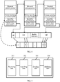
- FIG. 2 is a logic schematic diagram of a buffer according to the present invention, where the buffer mainly includes two parts: a buffer header (buffer_head) and a buffer data area (buffer_data), where the buffer header includes all information required by a processor for operating the buffer.
- the buffer header includes: a physical address pointer (b_blocknr), a pointer pointing to a next buffer (b_reqnext), and a buffer data area pointer (b_data), where b_blocknr is used to store a physical address of data in the buffer data area in a flash memory, b_reqnext is used to store an address of the next buffer, and b_data is used to store an address and a size of the buffer data area.
- buffer_data is a buffer data area that corresponds to the buffer header and is used to store data, and data in the buffer data area corresponds to a block in the flash memory. A size of each buffer_data is not fixed.
- the buffer header and the buffer data area are dynamically established in a process of reading data, and information about the buffer header and data buffered in the buffer data area are also dynamically filled.
- the processor needs to process multiple different instructions for reading data (that is, needs to read different pieces of data multiple times), multiple buffers need to be established. Therefore, when the processor receives a read data instruction the first time, no buffer exists in internal memory.
- each buffer includes a buffer header and a buffer data area. If the processor receives a read data instruction again, the processor scans established buffer headers in order, and compares physical addresses buffered in the established buffer headers with a physical address in the newly received read data instruction, and if a comparison result is that the two are the same, directly returns data in buffer data areas that correspond to the buffer headers, and if the comparison result is that the two are different, it indicates that the physical address is not found in the established buffer headers.
- S130 may be performed by the processor of the user equipment.
- the actual physical block size of the flash memory is acquired by a driver layer (Host Layer) of the flash memory from a correspondence table between identifier information (Card IDentity, CID) of the flash memory and the actual physical block size of the flash memory according to the identifier information CID of the flash memory.
- identifier information Card IDentity, CID
- CID Card IDentity
- a specific establishment process is that: preset identifier information of the flash memory is acquired from a data sheet (Data sheet) of an manufacturer by using a standard command, and then a manufacturer ID is acquired from the acquired preset identifier information of the flash memory, and after the manufacturer ID is acquired, a model of the flash memory is further acquired from the CID according to the manufacturer ID, and then it is determined whether the model of the flash memory is in a lookup table (Look-Up-Table, LUT), and if yes, an actual physical block size of the flash memory in the LUT table is returned; otherwise, a default value 512 bytes is returned. After the actual physical block size of the flash memory or the default value is acquired, the table of the correspondence between the identifier information CID of the flash memory and the actual physical block size of the flash memory can be established.
- Data sheet data sheet
- a manufacturer ID is acquired from the acquired preset identifier information of the flash memory
- a model of the flash memory is further acquired from the CID according to the manufacturer ID, and then it is determined
- the driver layer of the flash memory feeds back the acquired actual physical block size of the flash memory to a block device layer (Block Layer) of the flash memory, and finally sends the actual physical block size of the flash memory by using the block device layer to the processor by using a submit_bio interface function.
- Block Layer block device layer
- the buffer data area is divided from the internal memory, that is, the buffer data area is established. Specifically, partial space in the internal memory is used as the buffer data area, and the space is indicated by using a start address and an end address. For example, a size of the internal memory is 4 G, where no data is stored between an address 2000 KB and an address 4000 KB, so that the processor may divide 2000 KB to 2008 KB from the space, and space of total 8 KB is used as the buffer data area.
- the processor needs to establish a buffer, where a size of a buffer data area of the buffer is greater than the size of the to-be-read data, and the size of the buffer data area is an integer multiple of the actual physical block size of the flash memory, or a size of a buffer data area is equal to the size of the to-be-read data, and the size of the buffer data area is an integer multiple of the actual physical block size of the flash memory.
- the actual physical block size of the flash memory is 8 K.
- the size of the to-be-read data is 2 K
- a size of the buffer data area divided from the internal memory is 8 K
- the size of the buffer data area is one time of the actual physical block size of the flash memory
- the size of the to-be-read data is 22 K
- the size of the buffer data area divided from the internal memory is 24 K
- the size of the buffer data area is three times of the actual physical block size of the flash memory.
- the method further includes:
- S140 The user equipment reads the to-be-read data from the flash memory according to the physical address and buffers the to-be-read data into the buffer data area.
- S140 may be performed by the processor of the user equipment.
- the processor sends a block device read request to the driver layer of the flash memory by using the submit_bio interface function, where the read request includes the physical address.
- the block device layer of the flash memory receives the block device read request by using an mmc_request interface function, and after receiving the block device read request, the block device layer of the flash memory sends a read command to the driver layer of the flash memory, where the read command includes the physical address, and the driver layer of the flash memory acquires the to-be-read data from the flash memory according to the physical address in the received read command.
- the driver layer of the flash memory After acquiring the to-be-read data, the driver layer of the flash memory sends the to-be-read data to the block device layer of the flash memory; after receiving the to-be-read data, the block device layer of the flash memory buffers the to-be-read data into a physical buffer, and forwards the to-be-read data to the processor; and after receiving the to-be-read data, the processor buffers the to-be-read data into the divided buffer data area and returns the to-be-read data to an upper-layer application.
- a buffer data area is applied for according to an actual physical block size of the flash memory, which achieves an objective of dynamically adjusting the buffer data area, that is, unifying a unit of reading, by a processor, data from the flash memory and a unit of reading data inside the flash memory, thereby resolving problems of low reading efficiency of the flash memory and a short service life of the flash memory.
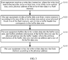
- FIG. 3 is a flowchart of a method for writing data into a flash memory according to Embodiment 2 of the present invention. As shown in FIG. 3 , the method specifically includes:
- S310 may be performed by a processor of the user equipment.
- a flash memory is a form of an electrically-erasable programmable read only memory and is allowed to be erased or written multiple times in an operation, and the flash memory is a non-volatile memory.
- the flash memory is a storage medium that user equipment uses to permanently store data.
- the flash memory is an NAND flash
- the NAND flash is built into an eMMC.
- S320 The user equipment divides a buffer data area from internal memory according to the size of the to-be-written data and an actual physical block size of the flash memory, and divides a buffer header that corresponds to the buffer data area.
- S320 may be performed by the processor of the user equipment.
- the buffer header and the buffer data area are dynamically established in a process of writing data into the flash memory, and information about the buffer header and data buffered in the buffer data area are also dynamically filled.
- the processor needs to process multiple different instructions for writing data (that is, needs to write different pieces of data multiple times)
- multiple buffers need to be established. Therefore, when the processor receives a write data instruction the first time, no buffer exists in the internal memory.
- the processor already writes multiple different pieces of data into the flash memory, multiple buffers are established, and each buffer includes a buffer header and a buffer data area.
- a size of the buffer data area is greater than the size of the to-be-read data, and the size of the buffer data area is an integer multiple of the actual physical block size of the flash memory, or a size of the buffer data area is equal to the size of the to-be-read data, and the size of the buffer data area is an integer multiple of the actual physical block size of the flash memory.
- the user equipment buffers the to-be-written data into the buffer data area, and buffers attribute information of the buffer data area and the physical address into the buffer header, where the attribute information of the buffer data area includes an address and a size of the buffer data area.
- S330 may be performed by the processor of the user equipment.
- a start address of the buffer data area is 200 K
- the size is 24 K
- the start address 200 K and the size 24 K are stored in the buffer header that corresponds to the buffer data area.
- S340 The user equipment writes the to-be-written data into the flash memory according to the physical address.
- S340 may be performed by the processor of the user equipment.
- the writing the to-be-written data into the flash memory according to the physical address is specifically:
- the block device layer of the flash memory After receiving the information indicating that the writing is successful, the block device layer of the flash memory forwards the information indicating that the writing is successful to the processor; and finally, the processor returns the information indicating that the writing is successful to an upper-layer application and waits to receive a next write data instruction.
- a buffer data area is applied for according to an actual physical block size of the flash memory, which achieves an objective of dynamically adjusting the buffer data area, that is, unifying a unit of writing, by a processor, data into the flash memory and a unit of writing data inside the flash memory, thereby resolving problems of low writing efficiency of the flash memory and a short service life of the flash memory.
- the method may further include the following steps:
- the adding identifier information to the buffer data area is specifically: adding the identifier information to the buffer data area by using the actual physical block size of the flash memory as a unit. As shown in FIG. 4 , it is assumed that the actual physical block size of the flash memory is 8 K, and because 8 K is one time of the actual physical block size of the flash memory, one piece of identifier information is added; 16 K is two times of the actual physical block size of the flash memory, two pieces of identifier information are added; and 24 K is three times of the actual physical block size of the flash memory, three pieces of identifier information are added.
- S360 When an occupancy rate of the internal memory is greater than a preset first threshold, write, into the flash memory, data in the buffer data area that corresponds to the identifier information being the information indicating dirty data; or when a time that the buffer data area resides is greater than a preset second threshold, write, into the flash memory, data in the buffer data area that corresponds to the identifier information being the information indicating dirty data.
- a flush daemon may detect all buffer data areas that are identified as information indicating dirty data in buffer headers at the same time, so that data in the buffer data areas is written into the flash memory.
- FIG. 5 is a schematic diagram of an apparatus for reading data from a flash memory according to Embodiment 3 of the present invention.
- the apparatus may be used to perform the method shown in FIG. 1 .
- the apparatus includes: a receiving unit 501, a searching unit 502, a dividing unit 503, and a buffering unit 504, where the receiving unit 501 is configured to receive a read data instruction, where the read data instruction includes: a size of to-be-read data and a physical address of the to-be-read data in the flash memory; the searching unit 502 is configured to search a buffer for the physical address received by the receiving unit 501; the dividing unit 503 is configured to: when the searching unit 502 does not find the physical address in the buffer, divide a buffer data area from internal memory according to the size of the to-be-read data and an actual physical block size of the flash memory; and the buffering unit 504 is configured to read the to-be-read data from the flash memory according to the physical address and buffer the to-be-read data into
- the dividing unit 503 is further configured to:
- the receiving unit 501 is further configured to receive the actual physical block size of the flash memory that is sent by the driver layer of the flash memory by using a block device layer of the flash memory.
- FIG. 6 is a schematic diagram of an apparatus for writing data into a flash memory according to Embodiment 4 of the present invention.
- the apparatus may be used to perform the method shown in FIG. 3 .
- the apparatus includes: a receiving unit 601, a dividing unit 602, a buffering unit 603, and a writing unit 604, where the receiving unit 601 is configured to receive a write data instruction, where the write data instruction includes: to-be-written data, a size of the to-be-written data, and a physical address of the to-be-written data in the flash memory;
- the dividing unit 602 is configured to divide a buffer data area from internal memory according to the size of the to-be-written data received by the receiving unit 601 and an actual physical block size of the flash memory, and divide a buffer header that corresponds to the buffer data area;
- the buffering unit 603 is configured to buffer the to-be-written data into the buffer data area divided by the dividing unit 602, and buffer attribute information of the buffer data area and the physical address into the
- the apparatus further includes: an adding unit 605, configured to add identifier information to the buffer data area, and when data in the buffer data area is not consistent with data in the flash memory, identify the identifier information as information indicating dirty data.
- an adding unit 605 configured to add identifier information to the buffer data area, and when data in the buffer data area is not consistent with data in the flash memory, identify the identifier information as information indicating dirty data.
- the writing unit 604 is further configured to: when an occupancy rate of the internal memory is greater than a preset first threshold, write, into the flash memory, data in the buffer data area that corresponds to the identifier information, being the information indicating dirty data, added by the adding unit; or when a time that the buffer data area resides is greater than a preset second threshold, write, into the flash memory, data in the buffer data area that corresponds to the identifier information, being the information indicating dirty data, added by the adding unit.
- a buffer data area is applied for according to an actual physical block size of the flash memory, which achieves an objective of dynamically adjusting the buffer data area, that is, unifying a unit of reading/writing, by a processor, data from/into the flash memory and a unit of reading/writing data inside the flash memory, thereby resolving problems of low reading and writing efficiency of the flash memory and a short service life of the flash memory.
- FIG. 7 is a schematic diagram of user equipment according to Embodiment 5 of the present invention.
- the equipment includes: a network interface 701, one or more processors 702, a storage 703, and a system bus 704 configured to connect to the network interface 701, the processor 702, and the memory 703.
- the processor 702 may be a CPU.
- the network interface 701 is configured to communicate with another device.
- the storage 703 includes: internal memory and a flash memory.
- One or more programs are stored in the storage 703 and are configured to be executed by the one or more processors 702, where the one or more programs include:
- a size of the buffer data area is greater than the size of the to-be-read data, and the size of the buffer data area is an integer multiple of the actual physical block size of the flash memory.
- a size of the buffer data area is equal to the size of the to-be-read data, and the size of the buffer data area is an integer multiple of the actual physical block size of the flash memory.
- the one or more programs further include: dividing a buffer header that corresponds to the buffer data area from the internal memory, and buffering attribute information of the buffer data area and the physical address into the buffer header, where the attribute information of the buffer data area includes an address and the size of the buffer data area.
- the actual physical block size of the flash memory is acquired by a driver layer of the flash memory from a correspondence table between identifier information CID of the flash memory and the actual physical block size of the flash memory according to the identifier information CID of the flash memory.
- the one or more programs further include: receiving the actual physical block size of the flash memory that is sent by the driver layer of the flash memory by using a block device layer of the flash memory.
- FIG. 8 is a schematic diagram of user equipment according to Embodiment 6 of the present invention.
- the equipment includes: a network interface 801, one or more processors 802, a memory 803, and a system bus 804 configured to connect to the network interface 801, the processor 802, and the storage 803.
- the processor 802 may be a CPU.
- the network interface 801 is configured to communicate with another device.
- the storage 803 includes: internal memory and a flash memory.
- One or more programs are stored in the storage 803 and are configured to be executed by the one or more processors 802, where the one or more programs include:
- the one or more programs further include:
- a buffer data area is applied for according to an actual physical block size of a flash memory, which achieves an objective of dynamically adjusting the buffer data area, that is, unifying a unit of reading/writing, by a processor, data from/into the flash memory and a unit of reading/writing data inside the flash memory, thereby resolving problems of low reading and writing efficiency of the flash memory and a short service life of the flash memory.
- Steps of methods or algorithms described in the embodiments disclosed in this specification may be implemented by hardware, a software module executed by a processor, or a combination thereof.
- the software module may reside in a random access memory (RAM), a memory, a read-only memory (ROM), an electrically programmable ROM, an electrically erasable programmable ROM, a register, a hard disk, a removable disk, a CD-ROM, or any other form of storage medium known in the art.
Landscapes
- Engineering & Computer Science (AREA)
- Theoretical Computer Science (AREA)
- Physics & Mathematics (AREA)
- General Engineering & Computer Science (AREA)
- General Physics & Mathematics (AREA)
- Human Computer Interaction (AREA)
- Techniques For Improving Reliability Of Storages (AREA)
- Memory System (AREA)
- Memory System Of A Hierarchy Structure (AREA)
- Microelectronics & Electronic Packaging (AREA)
- Information Retrieval, Db Structures And Fs Structures Therefor (AREA)
Abstract
Description
- The present invention relates to the field of data processing, and in particular, to a method and an apparatus for reading/writing data from/into a flash memory, and user equipment.
- Currently, embedded multimedia cards (embedded Multi Media Card, eMMC) are widely used as main storage mediums of mobile phones, and an internal storage device of an eMMC is a non-linear flash memory (NAND flash), which is referred to as a flash memory for short. An NAND flash reads and writes data in a unit of page, and erases data in a unit of block. At first, a page of an NAND flash is of 512 bytes. However, with development of an NAND flash process, a capacity of the NAND flash becomes increasingly large, and a size of a page is also increased to 8 kilo bytes (8 KB or 8 K for short) or 16 K. The eMMC is a standard and uniform protocol, and a specified unit of reading/writing is 512 bytes. As a result, a write amplification factor is increased and operation efficiency and a service life of the eMMC are affected.
- In the prior art, to be compatible with eMMCs of different manufacturers and types, in a Linux system, physical blocks are uniform in size, for example, 512 bytes, by using an eMMC driver. In this way, because a unit of reading/writing of an NAND flash is page, that is, 8 KB or 16 KB, although the eMMC reads/writes 512 bytes, operations are amplified to 8 K or 16 K for the NAND flash, leading to problems of low reading and writing efficiency of the eMMC and a short service life of the eMMC.
- Embodiments of the present invention provide a method and an apparatus for reading/writing data from/into a flash memory, and user equipment, which can resolve problems of low reading and writing efficiency of the flash memory and a short service life of the flash memory.
- According to a first aspect, a method for reading data from a flash memory is provided, where the method includes:
- receiving a read data instruction, where the read data instruction includes: a size of to-be-read data and a physical address of the to-be-read data in the flash memory;
- searching a buffer for the physical address;
- when the physical address is not found in the buffer, dividing a buffer data area from internal memory according to the size of the to-be-read data and an actual physical block size of the flash memory; and
- reading the to-be-read data from the flash memory according to the physical address and buffering the to-be-read data into the buffer data area.
- With reference to the first aspect, in a first implementation manner of the first aspect, a size of the buffer data area is greater than the size of the to-be-read data, and the size of the buffer data area is an integer multiple of the actual physical block size of the flash memory.
- With reference to the first aspect, in a second implementation manner of the first aspect, a size of the buffer data area is equal to the size of the to-be-read data, and the size of the buffer data area is an integer multiple of the actual physical block size of the flash memory.
- With reference to the first implementation manner of the first aspect or the second implementation manner of the first aspect, in a third implementation manner of the first aspect, after the dividing a buffer data area from internal memory and before the reading the to-be-read data from the flash memory according to the physical address, the method further includes:
- dividing a buffer header that corresponds to the buffer data area from the internal memory, and buffering attribute information of the buffer data area and the physical address into the buffer header, where the attribute information of the buffer data area includes an address and the size of the buffer data area.
- With reference to the first aspect or any implementation manner of the foregoing three implementation manners of the first aspect, in a fourth implementation manner of the first aspect, the actual physical block size of the flash memory is acquired by a driver layer of the flash memory from a correspondence table between identifier information CID of the flash memory and the actual physical block size of the flash memory according to the identifier information CID of the flash memory.
- With reference to the first aspect, in a fifth implementation manner of the first aspect, before the receiving a read data instruction, the method further includes: receiving the actual physical block size of the flash memory that is sent by the driver layer of the flash memory by using a block device layer of the flash memory.
- According to a second aspect, a method for writing data into a flash memory is provided, where the method includes:
- receiving a write data instruction, where the write data instruction includes: to-be-written data, a size of the to-be-written data, and a physical address of the to-be-written data in the flash memory;
- dividing a buffer data area from internal memory according to the size of the to-be-written data and an actual physical block size of the flash memory, and dividing a buffer header that corresponds to the buffer data area;
- buffering the to-be-written data into the buffer data area, and buffering attribute information of the buffer data area and the physical address into the buffer header, where the attribute information of the buffer data area includes an address and a size of the buffer data area; and
- writing the to-be-written data into the flash memory according to the physical address.
- With reference to the second aspect, in a first implementation manner of the second aspect, the method further includes:
- adding identifier information to the buffer data area, and when data in the buffer data area is not consistent with data in the flash memory, identifying the identifier information as information indicating dirty data; and
- when an occupancy rate of the internal memory is greater than a preset first threshold, writing, into the flash memory, data in the buffer data area that corresponds to the identifier information being the information indicating dirty data; or
- when a time that the buffer data area resides is greater than a preset second threshold, writing, into the flash memory, data in the buffer data area that corresponds to the identifier information being the information indicating dirty data.
- According to a third aspect, an apparatus for reading data from a flash memory is provided, where the apparatus includes: a receiving unit, a searching unit, a dividing unit, and a buffering unit, where
the receiving unit is configured to receive a read data instruction, where the read data instruction includes: a size of to-be-read data and a physical address of the to-be-read data in the flash memory;
the searching unit is configured to search a buffer for the physical address received by the receiving unit;
the dividing unit is configured to: when the searching unit does not find the physical address in the buffer, divide a buffer data area from internal memory according to the size of the to-be-read data and an actual physical block size of the flash memory; and
the buffering unit is configured to read the to-be-read data from the flash memory according to the physical address and buffer the to-be-read data into the buffer data area divided by the dividing unit. - With reference to the third aspect, in a first implementation manner of the third aspect, the dividing unit is further configured to:
- divide a buffer header that corresponds to the buffer data area from the internal memory, and buffer attribute information of the buffer data area and the physical address to the buffer header, where the attribute information of the buffer data area includes an address and a size of the buffer data area, where
- the size of the buffer data area is greater than the size of the to-be-read data, and the size of the buffer data area is an integer multiple of the actual physical block size of the flash memory; or
- the size of the buffer data area is equal to the size of the to-be-read data, and the size of the buffer data area is an integer multiple of the actual physical block size of the flash memory; and
- the actual physical block size of the flash memory is acquired by a driver layer of the flash memory from a correspondence table between identifier information CID of the flash memory and the actual physical block size of the flash memory according to the identifier information CID of the flash memory.
- With reference to the third aspect or the first implementation manner of the third aspect, in a second implementation manner of the third aspect, the receiving unit is further configured to receive the actual physical block size of the flash memory that is sent by the driver layer of the flash memory by using a block device layer of the flash memory.
- According to a fourth aspect, an apparatus for writing data into a flash memory is provided, where the apparatus includes: a receiving unit, a dividing unit, a buffering unit, and a writing unit, where
the receiving unit is configured to receive a write data instruction, where the write data instruction includes: to-be-written data, a size of the to-be-written data, and a physical address of the to-be-written data in the flash memory;
the dividing unit is configured to divide a buffer data area from internal memory according to the size of the to-be-written data and an actual physical block size of the flash memory received by the receiving unit, and divide a buffer header that corresponds to the buffer data area;
the buffering unit is configured to buffer the to-be-written data into the buffer data area divided by the dividing unit, and buffer attribute information of the buffer data area and the physical address into the buffer header divided by the dividing unit, where the attribute information of the buffer data area includes a logical address and a size of the buffer data area; and
the writing unit is configured to write the to-be-written data into the flash memory according to the physical address. - With reference to the fourth aspect, in a first implementation manner of the fourth aspect, the apparatus further includes: an adding unit, configured to add identifier information to the buffer data area, and when data in the buffer data area is not consistent with data in the flash memory, identify the identifier information as information indicating dirty data, where
the writing unit is further configured to: when an occupancy rate of the internal memory is greater than a preset first threshold, write, into the flash memory, data in the buffer data area that corresponds to the identifier information, being the information indicating dirty data, added by the adding unit; or
when a time that the buffer data area resides is greater than a preset second threshold, write, into the flash memory, data in the buffer data area that corresponds to the identifier information, being the information indicating dirty data, added by the adding unit. - According to a fifth aspect, user equipment is provided, where the equipment includes:
- a network interface;
- one or more processors;
- a storage, where the storage includes internal memory and a flash memory; and
- one or more programs, stored in the storage and configured to be executed by the one or more processors, where the one or more programs include:
- receiving a read data instruction, where the read data instruction includes: a size of to-be-read data and a physical address of the to-be-read data in the flash memory;
- searching a buffer for the physical address;
- when the physical address is not found in the buffer, dividing a buffer data area from the internal memory according to the size of the to-be-read data and an actual physical block size of the flash memory; and
- reading the to-be-read data from the flash memory according to the physical address and buffering the to-be-read data into the buffer data area.
- With reference to the fifth aspect, in a first implementation manner of the fifth aspect, a size of the buffer data area is greater than the size of the to-be-read data, and the size of the buffer data area is an integer multiple of the actual physical block size of the flash memory.
- With reference to the fifth aspect, in a second implementation manner of the fifth aspect, a size of the buffer data area is equal to the size of the to-be-read data, and the size of the buffer data area is an integer multiple of the actual physical block size of the flash memory.
- With reference to the first implementation manner of the fifth aspect or the second implementation manner of the fifth aspect, in a third implementation manner of the fifth aspect, the one or more programs further include: dividing a buffer header that corresponds to the buffer data area from the internal memory, and buffering attribute information of the buffer data area and the physical address into the buffer header, where the attribute information of the buffer data area includes an address and the size of the buffer data area.
- With reference to the fifth aspect or any implementation manner of the foregoing three implementation manners of the fifth aspect, in a fourth implementation manner of the fifth aspect, the actual physical block size of the flash memory is acquired by a driver layer of the flash memory from a correspondence table between identifier information CID of the flash memory and the actual physical block size of the flash memory according to the identifier information CID of the flash memory.
- With reference to the fifth aspect, in a fifth implementation manner of the fifth aspect, the one or more programs further include: receiving the actual physical block size of the flash memory that is sent by the driver layer of the flash memory by using a block device layer of the flash memory.
- According to a sixth aspect, user equipment is provided, where the equipment includes:
- a network interface;
- one or more processors;
- a storage, where the storage includes internal memory and a flash memory; and
- one or more programs, stored in the storage and configured to be executed by the one or more processors, where the one or more programs include:
- receiving a write data instruction, where the write data instruction includes: to-be-written data, a size of the to-be-written data, and a physical address of the to-be-written data in the flash memory;
- dividing a buffer data area from internal memory according to the size of the to-be-written data and an actual physical block size of the flash memory, and dividing a buffer header that corresponds to the buffer data area;
- buffering the to-be-written data into the buffer data area, and buffering attribute information of the buffer data area and the physical address into the buffer header, where the attribute information of the buffer data area includes an address and a size of the buffer data area; and
- writing the to-be-written data into the flash memory according to the physical address.
- With reference to the sixth aspect, in a first implementation manner of the sixth aspect, the one or more programs further includes:
- adding identifier information to the buffer data area, and when data in the buffer data area is not consistent with data in the flash memory, identifying the identifier information as information indicating dirty data; and
- when an occupancy rate of the internal memory is greater than a preset first threshold, writing, into the flash memory, data in the buffer data area that corresponds to the identifier information being the information indicating dirty data; or
- when a time that the buffer data area resides is greater than a preset second threshold, writing, into the flash memory, data in the buffer data area that corresponds to the identifier information being the information indicating dirty data.
- In the method and the apparatus for reading/writing data from/into a flash memory, and the user equipment that are provided by the embodiments of the present invention, a buffer data area is applied for according to an actual physical block size of the flash memory, which achieves an objective of dynamically adjusting the buffer data area, that is, unifying a unit of reading/writing, by a processor, data from/into the flash memory and a unit of reading/writing data inside the flash memory, thereby resolving problems of low reading and writing efficiency of the flash memory and a short service life of the flash memory.
-
-
FIG. 1 is a flowchart of a method for reading data from a flash memory according toEmbodiment 1 of the present invention; -
FIG. 2 is a logic schematic diagram of a buffer according to the present invention; -
FIG. 3 is a flowchart of a method for writing data into a flash memory according to Embodiment 2 of the present invention; -
FIG. 4 is a logic schematic diagram of a buffer after identifier information is added according to the present invention; -
FIG. 5 is a schematic diagram of an apparatus for reading data from a flash memory according to Embodiment 3 of the present invention; -
FIG. 6 is a schematic diagram of an apparatus for writing data into a flash memory according to Embodiment 4 of the present invention; -
FIG. 7 is a schematic diagram of user equipment according to Embodiment 5 of the present invention; and -
FIG. 8 is a schematic diagram of user equipment according to Embodiment 6 of the present invention. - To make the objectives, technical solutions, and advantages of the embodiments of the present invention clearer, the following clearly and completely describes the technical solutions in the embodiments of the present invention with reference to the accompanying drawings in the embodiments of the present invention. Apparently, the described embodiments are some but not all of the embodiments of the present invention. All other embodiments obtained by a person of ordinary skill in the art based on the embodiments of the present invention without creative efforts shall fall within the protection scope of the present invention.
- To provide thorough understanding of the present invention, the following further describes the embodiments of the present invention in detail with reference to the accompanying drawings. The foregoing embodiments are not intended to limit the protection scope of the present invention.
-
FIG. 1 is a flowchart of a method for reading data from a flash memory according toEmbodiment 1 of the present invention. As shown inFIG. 1 , the method specifically includes: - S110: User equipment receives a read data instruction, where the read data instruction includes: a size of to-be-read data and a physical address of the to-be-read data in the flash memory.
- Specifically, S110 may be performed by a processor of the user equipment.
- A flash memory is a form of an electrically-erasable programmable read only memory and is allowed to be erased or written multiple times in an operation, and the flash memory is a non-volatile memory. The flash memory is a storage medium that user equipment uses to permanently store data. In this specification, an example in which the flash memory is an NAND flash is used for description, and the NAND flash is built into an eMMC. When the user equipment reads data from the flash memory, data in the flash memory needs to be buffered in internal memory first; or when the user equipment writes data into the flash memory, the data also needs to be buffered in the internal memory, and then the data is written into the flash memory.
- It should be noted that, for eMMCs of different manufacturers, actual physical block sizes (Block sizes) of flash memories that correspond to the eMMCs are different. In addition, for different types of eMMCs, actual physical block sizes of flash memories that correspond to the eMMCs are also different. An actual physical block size of a flash memory is used to indicate a unit of reading/writing data inside an eMMC, and a larger value indicates better performance of data reading/writing inside the eMMC.
- S120: The user equipment searches a buffer for the physical address.
- Specifically, S120 may be performed by the processor of the user equipment.
- It should be noted that, a buffer buffer_cache is a part of internal memory, and in a Linux system, all free internal memory may be used as the buffer. The buffer is used to store data in a flash memory, so that access by a processor to the data in the flash memory is accelerated.
FIG. 2 is a logic schematic diagram of a buffer according to the present invention, where the buffer mainly includes two parts: a buffer header (buffer_head) and a buffer data area (buffer_data), where the buffer header includes all information required by a processor for operating the buffer. Specifically, the buffer header includes: a physical address pointer (b_blocknr), a pointer pointing to a next buffer (b_reqnext), and a buffer data area pointer (b_data), where b_blocknr is used to store a physical address of data in the buffer data area in a flash memory, b_reqnext is used to store an address of the next buffer, and b_data is used to store an address and a size of the buffer data area. buffer_data is a buffer data area that corresponds to the buffer header and is used to store data, and data in the buffer data area corresponds to a block in the flash memory. A size of each buffer_data is not fixed. It should be noted that the buffer header and the buffer data area are dynamically established in a process of reading data, and information about the buffer header and data buffered in the buffer data area are also dynamically filled. When the processor needs to process multiple different instructions for reading data (that is, needs to read different pieces of data multiple times), multiple buffers need to be established. Therefore, when the processor receives a read data instruction the first time, no buffer exists in internal memory. - It should be noted that when the processor already reads multiple different pieces of data, multiple buffers are established, and each buffer includes a buffer header and a buffer data area. If the processor receives a read data instruction again, the processor scans established buffer headers in order, and compares physical addresses buffered in the established buffer headers with a physical address in the newly received read data instruction, and if a comparison result is that the two are the same, directly returns data in buffer data areas that correspond to the buffer headers, and if the comparison result is that the two are different, it indicates that the physical address is not found in the established buffer headers.
- S130: When the user equipment does not find the physical address in the buffer, the user equipment divides a buffer data area from internal memory according to the size of the to-be-read data and an actual physical block size of the flash memory.
- Specifically, S130 may be performed by the processor of the user equipment.
- The actual physical block size of the flash memory is acquired by a driver layer (Host Layer) of the flash memory from a correspondence table between identifier information (Card IDentity, CID) of the flash memory and the actual physical block size of the flash memory according to the identifier information CID of the flash memory. The table of the correspondence between the identifier information CID of the flash memory and the actual physical block size of the flash memory is pre-established. A specific establishment process is that: preset identifier information of the flash memory is acquired from a data sheet (Data sheet) of an manufacturer by using a standard command, and then a manufacturer ID is acquired from the acquired preset identifier information of the flash memory, and after the manufacturer ID is acquired, a model of the flash memory is further acquired from the CID according to the manufacturer ID, and then it is determined whether the model of the flash memory is in a lookup table (Look-Up-Table, LUT), and if yes, an actual physical block size of the flash memory in the LUT table is returned; otherwise, a default value 512 bytes is returned. After the actual physical block size of the flash memory or the default value is acquired, the table of the correspondence between the identifier information CID of the flash memory and the actual physical block size of the flash memory can be established.
- Optionally, after acquiring the actual physical block size of the flash memory, the driver layer of the flash memory feeds back the acquired actual physical block size of the flash memory to a block device layer (Block Layer) of the flash memory, and finally sends the actual physical block size of the flash memory by using the block device layer to the processor by using a submit_bio interface function.
- The buffer data area is divided from the internal memory, that is, the buffer data area is established. Specifically, partial space in the internal memory is used as the buffer data area, and the space is indicated by using a start address and an end address. For example, a size of the internal memory is 4 G, where no data is stored between an address 2000 KB and an address 4000 KB, so that the processor may divide 2000 KB to 2008 KB from the space, and space of total 8 KB is used as the buffer data area.
- Specifically, when the physical address is not found in the buffer, it indicates that the processor does not read the to-be-read data before, that is, the to-be-read data is not buffered in the buffer data area. The processor needs to establish a buffer, where a size of a buffer data area of the buffer is greater than the size of the to-be-read data, and the size of the buffer data area is an integer multiple of the actual physical block size of the flash memory, or a size of a buffer data area is equal to the size of the to-be-read data, and the size of the buffer data area is an integer multiple of the actual physical block size of the flash memory. For example, the actual physical block size of the flash memory is 8 K. However, if the size of the to-be-read data is 2 K, a size of the buffer data area divided from the internal memory is 8 K, and the size of the buffer data area is one time of the actual physical block size of the flash memory; and if the size of the to-be-read data is 22 K, the size of the buffer data area divided from the internal memory is 24 K, and the size of the buffer data area is three times of the actual physical block size of the flash memory.
- Optionally, after the dividing a buffer data area from internal memory and before the reading the to-be-read data from the flash memory according to the physical address, the method further includes:
- dividing a buffer header that corresponds to the buffer data area from the internal memory, and buffering attribute information of the buffer data area and the physical address into the buffer header, where the attribute information of the buffer data area includes an address and the size of the buffer data area. For example, if a start address of the buffer data area is 200 K, and the size is 24 K, the start address 200 K and the
size 24 K are stored in the buffer header that corresponds to the buffer data area. - S140: The user equipment reads the to-be-read data from the flash memory according to the physical address and buffers the to-be-read data into the buffer data area.
- Specifically, S140 may be performed by the processor of the user equipment.
- Specifically, the processor sends a block device read request to the driver layer of the flash memory by using the submit_bio interface function, where the read request includes the physical address. The block device layer of the flash memory receives the block device read request by using an mmc_request interface function, and after receiving the block device read request, the block device layer of the flash memory sends a read command to the driver layer of the flash memory, where the read command includes the physical address, and the driver layer of the flash memory acquires the to-be-read data from the flash memory according to the physical address in the received read command.
- After acquiring the to-be-read data, the driver layer of the flash memory sends the to-be-read data to the block device layer of the flash memory; after receiving the to-be-read data, the block device layer of the flash memory buffers the to-be-read data into a physical buffer, and forwards the to-be-read data to the processor; and after receiving the to-be-read data, the processor buffers the to-be-read data into the divided buffer data area and returns the to-be-read data to an upper-layer application.
- In summary, in the method for reading data from a flash memory that is provided by this embodiment of the present invention, a buffer data area is applied for according to an actual physical block size of the flash memory, which achieves an objective of dynamically adjusting the buffer data area, that is, unifying a unit of reading, by a processor, data from the flash memory and a unit of reading data inside the flash memory, thereby resolving problems of low reading efficiency of the flash memory and a short service life of the flash memory.
-
FIG. 3 is a flowchart of a method for writing data into a flash memory according to Embodiment 2 of the present invention. As shown inFIG. 3 , the method specifically includes: - S310: User equipment receives a write data instruction, where the write data instruction includes: to-be-written data, a size of the to-be-written data, and a physical address of the to-be-written data in the flash memory.
- Specifically, S310 may be performed by a processor of the user equipment.
- A flash memory is a form of an electrically-erasable programmable read only memory and is allowed to be erased or written multiple times in an operation, and the flash memory is a non-volatile memory. The flash memory is a storage medium that user equipment uses to permanently store data. In this specification, an example in which the flash memory is an NAND flash is used for description, and the NAND flash is built into an eMMC. When the user equipment reads data from the flash memory, data in the flash memory needs to be buffered in internal memory first; or when the user equipment writes data into the flash memory, the data also needs to be buffered in the internal memory, and then the data is written into the flash memory.
- S320: The user equipment divides a buffer data area from internal memory according to the size of the to-be-written data and an actual physical block size of the flash memory, and divides a buffer header that corresponds to the buffer data area.
- Specifically, S320 may be performed by the processor of the user equipment.
- It should be noted that the buffer header and the buffer data area are dynamically established in a process of writing data into the flash memory, and information about the buffer header and data buffered in the buffer data area are also dynamically filled. When the processor needs to process multiple different instructions for writing data (that is, needs to write different pieces of data multiple times), multiple buffers need to be established. Therefore, when the processor receives a write data instruction the first time, no buffer exists in the internal memory. When the processor already writes multiple different pieces of data into the flash memory, multiple buffers are established, and each buffer includes a buffer header and a buffer data area.
- It should be noted that a size of the buffer data area is greater than the size of the to-be-read data, and the size of the buffer data area is an integer multiple of the actual physical block size of the flash memory, or a size of the buffer data area is equal to the size of the to-be-read data, and the size of the buffer data area is an integer multiple of the actual physical block size of the flash memory.
- S330: The user equipment buffers the to-be-written data into the buffer data area, and buffers attribute information of the buffer data area and the physical address into the buffer header, where the attribute information of the buffer data area includes an address and a size of the buffer data area.
- Specifically, S330 may be performed by the processor of the user equipment.
- For example, if a start address of the buffer data area is 200 K, and the size is 24 K, the start address 200 K and the
size 24 K are stored in the buffer header that corresponds to the buffer data area. - S340: The user equipment writes the to-be-written data into the flash memory according to the physical address.
- Specifically, S340 may be performed by the processor of the user equipment.
- The writing the to-be-written data into the flash memory according to the physical address is specifically:
- The processor sends a block device write request to a driver layer of the flash memory by using a submit_bio interface function, where the write request includes the physical address. A block device layer of the flash memory receives the block device write request by using an mmc_request interface function, and after receiving the block device write request, the block device layer of the flash memory forwards the block device write request to the driver layer of the flash memory, and finally, a driver layer related to the flash memory writes the to-be-written data into the flash memory according to the physical address and returns information indicating that the writing is successful to the block device layer of the flash memory.
- After receiving the information indicating that the writing is successful, the block device layer of the flash memory forwards the information indicating that the writing is successful to the processor; and finally, the processor returns the information indicating that the writing is successful to an upper-layer application and waits to receive a next write data instruction.
- In summary, in the method for writing data into a flash memory that is provided by this embodiment of the present invention, a buffer data area is applied for according to an actual physical block size of the flash memory, which achieves an objective of dynamically adjusting the buffer data area, that is, unifying a unit of writing, by a processor, data into the flash memory and a unit of writing data inside the flash memory, thereby resolving problems of low writing efficiency of the flash memory and a short service life of the flash memory.
- Optionally, the method may further include the following steps:
- S350: Add identifier information to the buffer data area, and when data in the buffer data area is not consistent with data in the flash memory, identify the identifier information as information indicating dirty data;
- Because of a buffering function of a buffer, an operation of data writing is actually delayed, and when the data in the buffer data area is newer than the data in the flash memory, the data is referred to as dirty data. In a specific implementation manner of the present invention, for adding identifier information to the buffer data area, refer to a logic schematic diagram of a buffer after identifier information is added, which is shown in
FIG. 4 . InFIG. 4 , three buffers are included, and each buffer includes a buffer header (buffer_head) and a buffer data area (buffer_data), where the buffer header includes b_blocknr, b_reqnext, identifier information (dirty), and b_data, where b_blocknr is used to store a physical address of data in a corresponding buffer data area in a flash memory, b_reqnext is used to store an address of a next buffer, dirty is newly added identifier information, and when the identifier information is 0, it indicates that the data in the corresponding buffer data area is normal data, and when the identifier information is 1, it indicates that the data in the corresponding buffer data area is dirty data; and b_data is used to store an address and a size of the corresponding buffer data area; buffer_data is a corresponding buffer data area and is used to store data, and a size of each buffer_data is not fixed, but buffer_data uses an actual physical block size of the flash memory as a unit. - The adding identifier information to the buffer data area is specifically: adding the identifier information to the buffer data area by using the actual physical block size of the flash memory as a unit. As shown in
FIG. 4 , it is assumed that the actual physical block size of the flash memory is 8 K, and because 8 K is one time of the actual physical block size of the flash memory, one piece of identifier information is added; 16 K is two times of the actual physical block size of the flash memory, two pieces of identifier information are added; and 24 K is three times of the actual physical block size of the flash memory, three pieces of identifier information are added. - S360: When an occupancy rate of the internal memory is greater than a preset first threshold, write, into the flash memory, data in the buffer data area that corresponds to the identifier information being the information indicating dirty data; or
when a time that the buffer data area resides is greater than a preset second threshold, write, into the flash memory, data in the buffer data area that corresponds to the identifier information being the information indicating dirty data. - In
FIG. 4 , when the buffer data area is identified as the information indicating dirty data, that is, a dirty value of the buffer data area is 0, there are two cases in which the data in the buffer data area is written back to the flash memory: - 1) when the occupancy rate of the internal memory is greater than the preset first threshold, the data in the buffer data area that corresponds to the identifier information being the information indicating dirty data is written into the flash memory; and
- 2) when the time that the buffer data area resides in the internal memory is greater than the preset second threshold, the data in the buffer data area that corresponds to the identifier information being the information indicating dirty data is written into the flash memory.
- By means of the foregoing two manners, it can be ensured that the data in the buffer data area does not reside in the internal memory indefinitely.
- It should be noted that a flush daemon (Flush daemon) may detect all buffer data areas that are identified as information indicating dirty data in buffer headers at the same time, so that data in the buffer data areas is written into the flash memory.
-
FIG. 5 is a schematic diagram of an apparatus for reading data from a flash memory according to Embodiment 3 of the present invention. The apparatus may be used to perform the method shown inFIG. 1 . InFIG. 5 , the apparatus includes: a receivingunit 501, a searchingunit 502, adividing unit 503, and abuffering unit 504, where
the receivingunit 501 is configured to receive a read data instruction, where the read data instruction includes: a size of to-be-read data and a physical address of the to-be-read data in the flash memory;
the searchingunit 502 is configured to search a buffer for the physical address received by the receivingunit 501;
thedividing unit 503 is configured to: when the searchingunit 502 does not find the physical address in the buffer, divide a buffer data area from internal memory according to the size of the to-be-read data and an actual physical block size of the flash memory; and
thebuffering unit 504 is configured to read the to-be-read data from the flash memory according to the physical address and buffer the to-be-read data into the buffer data area divided by the dividingunit 503. - Optionally, the dividing
unit 503 is further configured to: - divide a buffer header that corresponds to the buffer data area from the internal memory, and buffer attribute information of the buffer data area and the physical address to the buffer header, where the attribute information of the buffer data area includes an address and a size of the buffer data area, where
- the size of the buffer data area is greater than the size of the to-be-read data, and the size of the buffer data area is an integer multiple of the actual physical block size of the flash memory; or
- the size of the buffer data area is equal to the size of the to-be-read data, and the size of the buffer data area is an integer multiple of the actual physical block size of the flash memory; and the actual physical block size of the flash memory is acquired by a driver layer of the flash memory from a correspondence table between identifier information CID of the flash memory and the actual physical block size of the flash memory according to the identifier information CID of the flash memory.
- Optionally, the receiving
unit 501 is further configured to receive the actual physical block size of the flash memory that is sent by the driver layer of the flash memory by using a block device layer of the flash memory. -
FIG. 6 is a schematic diagram of an apparatus for writing data into a flash memory according to Embodiment 4 of the present invention. The apparatus may be used to perform the method shown inFIG. 3 . InFIG. 6 , the apparatus includes: a receivingunit 601, adividing unit 602, abuffering unit 603, and awriting unit 604, where
the receivingunit 601 is configured to receive a write data instruction, where the write data instruction includes: to-be-written data, a size of the to-be-written data, and a physical address of the to-be-written data in the flash memory;
thedividing unit 602 is configured to divide a buffer data area from internal memory according to the size of the to-be-written data received by the receivingunit 601 and an actual physical block size of the flash memory, and divide a buffer header that corresponds to the buffer data area;
thebuffering unit 603 is configured to buffer the to-be-written data into the buffer data area divided by the dividingunit 602, and buffer attribute information of the buffer data area and the physical address into the buffer header divided by the dividing unit, where the attribute information of the buffer data area includes a logical address and a size of the buffer data area; and
thewriting unit 604 is configured to write the to-be-written data into the flash memory according to the physical address. - Optionally, the apparatus further includes: an adding unit 605, configured to add identifier information to the buffer data area, and when data in the buffer data area is not consistent with data in the flash memory, identify the identifier information as information indicating dirty data.
- The
writing unit 604 is further configured to: when an occupancy rate of the internal memory is greater than a preset first threshold, write, into the flash memory, data in the buffer data area that corresponds to the identifier information, being the information indicating dirty data, added by the adding unit; or
when a time that the buffer data area resides is greater than a preset second threshold, write, into the flash memory, data in the buffer data area that corresponds to the identifier information, being the information indicating dirty data, added by the adding unit. - In the apparatus for reading data from a flash memory and the apparatus for writing data into a flash memory that are provided by the embodiments of the present invention, a buffer data area is applied for according to an actual physical block size of the flash memory, which achieves an objective of dynamically adjusting the buffer data area, that is, unifying a unit of reading/writing, by a processor, data from/into the flash memory and a unit of reading/writing data inside the flash memory, thereby resolving problems of low reading and writing efficiency of the flash memory and a short service life of the flash memory.
-
FIG. 7 is a schematic diagram of user equipment according to Embodiment 5 of the present invention. As shown inFIG. 7 , the equipment includes: anetwork interface 701, one ormore processors 702, astorage 703, and asystem bus 704 configured to connect to thenetwork interface 701, theprocessor 702, and thememory 703. - For example, the
processor 702 may be a CPU. - The
network interface 701 is configured to communicate with another device. - The
storage 703 includes: internal memory and a flash memory. One or more programs are stored in thestorage 703 and are configured to be executed by the one ormore processors 702, where the one or more programs include: - receiving a read data instruction, where the read data instruction includes: a size of to-be-read data and a physical address of the to-be-read data in the flash memory;
- searching a buffer for the physical address;
- when the physical address is not found in the buffer, dividing a buffer data area from the internal memory according to the size of the to-be-read data and an actual physical block size of the flash memory; and
- reading the to-be-read data from the flash memory according to the physical address and buffering the to-be-read data into the buffer data area.
- Optionally, a size of the buffer data area is greater than the size of the to-be-read data, and the size of the buffer data area is an integer multiple of the actual physical block size of the flash memory.
- Optionally, a size of the buffer data area is equal to the size of the to-be-read data, and the size of the buffer data area is an integer multiple of the actual physical block size of the flash memory.
- Further, the one or more programs further include: dividing a buffer header that corresponds to the buffer data area from the internal memory, and buffering attribute information of the buffer data area and the physical address into the buffer header, where the attribute information of the buffer data area includes an address and the size of the buffer data area.
- Optionally, the actual physical block size of the flash memory is acquired by a driver layer of the flash memory from a correspondence table between identifier information CID of the flash memory and the actual physical block size of the flash memory according to the identifier information CID of the flash memory.
- Further, the one or more programs further include: receiving the actual physical block size of the flash memory that is sent by the driver layer of the flash memory by using a block device layer of the flash memory.
-
FIG. 8 is a schematic diagram of user equipment according to Embodiment 6 of the present invention. As shown inFIG. 8 , the equipment includes: anetwork interface 801, one ormore processors 802, amemory 803, and asystem bus 804 configured to connect to thenetwork interface 801, theprocessor 802, and thestorage 803. - For example, the
processor 802 may be a CPU. - The
network interface 801 is configured to communicate with another device. - The
storage 803 includes: internal memory and a flash memory. One or more programs are stored in thestorage 803 and are configured to be executed by the one ormore processors 802, where the one or more programs include: - receiving a write data instruction, where the write data instruction includes: to-be-written data, a size of the to-be-written data, and a physical address of the to-be-written data in the flash memory;
- dividing a buffer data area from internal memory according to the size of the to-be-written data and an actual physical block size of the flash memory, and dividing a buffer header that corresponds to the buffer data area;
- buffering the to-be-written data into the buffer data area, and buffering attribute information of the buffer data area and the physical address into the buffer header, where the attribute information of the buffer data area includes an address and a size of the buffer data area; and
- writing the to-be-written data into the flash memory according to the physical address.
- Further, the one or more programs further include:
- adding identifier information to the buffer data area, and when data in the buffer data area is not consistent with data in the flash memory, identifying the identifier information as information indicating dirty data; and
- when an occupancy rate of the internal memory is greater than a preset first threshold, writing, into the flash memory, data in the buffer data area that corresponds to the identifier information being the information indicating dirty data; or
- when a time that the buffer data area resides is greater than a preset second threshold, writing, into the flash memory, data in the buffer data area that corresponds to the identifier information being the information indicating dirty data.
- In the user equipment that is provided by the embodiments of the present invention, a buffer data area is applied for according to an actual physical block size of a flash memory, which achieves an objective of dynamically adjusting the buffer data area, that is, unifying a unit of reading/writing, by a processor, data from/into the flash memory and a unit of reading/writing data inside the flash memory, thereby resolving problems of low reading and writing efficiency of the flash memory and a short service life of the flash memory.
- A person skilled in the art may be further aware that, in combination with the examples described in the embodiments disclosed in this specification, units and algorithm steps may be implemented by electronic hardware, computer software, or a combination thereof. To clearly describe the interchangeability between the hardware and the software, the foregoing has generally described compositions and steps of each example according to functions. Whether the functions are performed by hardware or software depends on particular applications and design constraint conditions of the technical solutions. A person skilled in the art may use different methods to implement the described functions for each particular application, but it should not be considered that the implementation goes beyond the scope of the present invention.
- Steps of methods or algorithms described in the embodiments disclosed in this specification may be implemented by hardware, a software module executed by a processor, or a combination thereof. The software module may reside in a random access memory (RAM), a memory, a read-only memory (ROM), an electrically programmable ROM, an electrically erasable programmable ROM, a register, a hard disk, a removable disk, a CD-ROM, or any other form of storage medium known in the art.
- In the foregoing specific implementation manners, the objective, technical solutions, and benefits of the present invention are further described in detail. It should be understood that the foregoing descriptions are merely specific implementation manners of the present invention, but are not intended to limit the protection scope of the present invention. Any modification, equivalent replacement, or improvement made without departing from the spirit and principle of the present invention should fall within the protection scope of the present invention.
Claims (21)
- A method for reading data from a flash memory, wherein the method comprises:receiving a read data instruction, wherein the read data instruction comprises: a size of to-be-read data and a physical address of the to-be-read data in the flash memory;searching a buffer for the physical address;when the physical address is not found in the buffer, dividing a buffer data area from internal memory according to the size of the to-be-read data and an actual physical block size of the flash memory; andreading the to-be-read data from the flash memory according to the physical address and buffering the to-be-read data into the buffer data area.
- The method according to claim 1, wherein a size of the buffer data area is greater than the size of the to-be-read data, and the size of the buffer data area is an integer multiple of the actual physical block size of the flash memory.
- The method according to claim 1, wherein a size of the buffer data area is equal to the size of the to-be-read data, and the size of the buffer data area is an integer multiple of the actual physical block size of the flash memory.
- The method according to claim 2 or 3, wherein after the dividing a buffer data area from internal memory and before the reading the to-be-read data from the flash memory according to the physical address, the method further comprises:dividing a buffer header that corresponds to the buffer data area from the internal memory, and buffering attribute information of the buffer data area and the physical address into the buffer header, wherein the attribute information of the buffer data area comprises an address and the size of the buffer data area.
- The method according to any one of claims 1 to 4, wherein the actual physical block size of the flash memory is acquired by a driver layer of the flash memory from a correspondence table between identifier information CID of the flash memory and the actual physical block size of the flash memory according to the identifier information CID of the flash memory.
- The method according to claim 1, wherein before the receiving a read data instruction, the method further comprises: receiving the actual physical block size of the flash memory that is sent by the driver layer of the flash memory by using a block device layer of the flash memory.
- A method for writing data into a flash memory, wherein the method comprises:receiving a write data instruction, wherein the write data instruction comprises:to-be-written data, a size of the to-be-written data, and a physical address of the to-be-written data in the flash memory;dividing a buffer data area from internal memory according to the size of the to-be-written data and an actual physical block size of the flash memory, and dividing a buffer header that corresponds to the buffer data area;buffering the to-be-written data into the buffer data area, and buffering attribute information of the buffer data area and the physical address into the buffer header, wherein the attribute information of the buffer data area comprises an address and a size of the buffer data area; andwriting the to-be-written data into the flash memory according to the physical address.
- The method according to claim 7, wherein the method further comprises:adding identifier information to the buffer data area, and when data in the buffer data area is not consistent with data in the flash memory, identifying the identifier information as information indicating dirty data; andwhen an occupancy rate of the internal memory is greater than a preset first threshold, writing, into the flash memory, data in the buffer data area that corresponds to the identifier information being the information indicating dirty data; orwhen a time that the buffer data area resides is greater than a preset second threshold, writing, into the flash memory, data in the buffer data area that corresponds to the identifier information being the information indicating dirty data.
- An apparatus for reading data from a flash memory, wherein the apparatus comprises: a receiving unit, a searching unit, a dividing unit, and a buffering unit, wherein
the receiving unit is configured to receive a read data instruction, wherein the read data instruction comprises: a size of to-be-read data and a physical address of the to-be-read data in the flash memory;
the searching unit is configured to search a buffer for the physical address received by the receiving unit;
the dividing unit is configured to: when the searching unit does not find the physical address in the buffer, divide a buffer data area from internal memory according to the size of the to-be-read data and an actual physical block size of the flash memory; and
the buffering unit is configured to read the to-be-read data from the flash memory according to the physical address and buffer the to-be-read data into the buffer data area divided by the dividing unit. - The apparatus according to claim 9, wherein the dividing unit is further configured to:divide a buffer header that corresponds to the buffer data area from the internal memory, and buffer attribute information of the buffer data area and the physical address to the buffer header, wherein the attribute information of the buffer data area comprises an address and a size of the buffer data area, whereinthe size of the buffer data area is greater than the size of the to-be-read data, and the size of the buffer data area is an integer multiple of the actual physical block size of the flash memory; orthe size of the buffer data area is equal to the size of the to-be-read data, and the size of the buffer data area is an integer multiple of the actual physical block size of the flash memory; andthe actual physical block size of the flash memory is acquired by a driver layer of the flash memory from a correspondence table between identifier information CID of the flash memory and the actual physical block size of the flash memory according to the identifier information CID of the flash memory.
- The apparatus according to claim 9 or 10, wherein the receiving unit is further configured to receive the actual physical block size of the flash memory that is sent by the driver layer of the flash memory by using a block device layer of the flash memory.
- An apparatus for writing data into a flash memory, wherein the apparatus comprises: a receiving unit, a dividing unit, a buffering unit, and a writing unit, wherein
the receiving unit is configured to receive a write data instruction, wherein the write data instruction comprises: to-be-written data, a size of the to-be-written data, and a physical address of the to-be-written data in the flash memory;
the dividing unit is configured to divide a buffer data area from internal memory according to the size of the to-be-written data and an actual physical block size of the flash memory received by the receiving unit, and divide a buffer header that corresponds to the buffer data area;
the buffering unit is configured to buffer the to-be-written data into the buffer data area divided by the dividing unit, and buffer attribute information of the buffer data area and the physical address into the buffer header divided by the dividing unit, wherein the attribute information of the buffer data area comprises a logical address and a size of the buffer data area; and
the writing unit is configured to write the to-be-written data into the flash memory according to the physical address. - The apparatus according to claim 12, wherein the apparatus further comprises: an adding unit, configured to add identifier information to the buffer data area, and when data in the buffer data area is not consistent with data in the flash memory, identify the identifier information as information indicating dirty data, wherein
the writing unit is further configured to: when an occupancy rate of the internal memory is greater than a preset first threshold, write, into the flash memory, data in the buffer data area that corresponds to the identifier information, being the information indicating dirty data, added by the adding unit; or
when a time that the buffer data area resides is greater than a preset second threshold, write, into the flash memory, data in the buffer data area that corresponds to the identifier information, being the information indicating dirty data, added by the adding unit. - User equipment, wherein the equipment comprises:a network interface;one or more processors;a storage, wherein the storage comprises internal memory and a flash memory; andone or more programs, stored in the storage and configured to be executed by the one or more processors, wherein the one or more programs comprise:receiving a read data instruction, wherein the read data instruction comprises: a size of to-be-read data and a physical address of the to-be-read data in the flash memory;searching a buffer for the physical address;when the physical address is not found in the buffer, dividing a buffer data area from the internal memory according to the size of the to-be-read data and an actual physical block size of the flash memory; andreading the to-be-read data from the flash memory according to the physical address and buffering the to-be-read data into the buffer data area.
- The equipment according to claim 14, wherein a size of the buffer data area is greater than the size of the to-be-read data, and the size of the buffer data area is an integer multiple of the actual physical block size of the flash memory.
- The equipment according to claim 14, wherein a size of the buffer data area is equal to the size of the to-be-read data, and the size of the buffer data area is an integer multiple of the actual physical block size of the flash memory.
- The equipment according to claim 15 or 16, wherein the one or more programs further comprise: dividing a buffer header that corresponds to the buffer data area from the internal memory, and buffering attribute information of the buffer data area and the physical address into the buffer header, wherein the attribute information of the buffer data area comprises an address and the size of the buffer data area.
- The equipment according to any one of claims 14 to 17, wherein the actual physical block size of the flash memory is acquired by a driver layer of the flash memory from a correspondence table between identifier information CID of the flash memory and the actual physical block size of the flash memory according to the identifier information CID of the flash memory.
- The equipment according to claim 14, wherein the one or more programs further comprise: receiving the actual physical block size of the flash memory that is sent by the driver layer of the flash memory by using a block device layer of the flash memory.
- User equipment, wherein the equipment comprises:a network interface;one or more processors;a storage, wherein the storage comprises internal memory and a flash memory; andone or more programs, stored in the storage and configured to be executed by the one or more processors, wherein the one or more programs comprise:receiving a write data instruction, wherein the write data instruction comprises:to-be-written data, a size of the to-be-written data, and a physical address of the to-be-written data in the flash memory;dividing a buffer data area from internal memory according to the size of the to-be-written data and an actual physical block size of the flash memory, and dividing a buffer header that corresponds to the buffer data area;buffering the to-be-written data into the buffer data area, and buffering attribute information of the buffer data area and the physical address into the buffer header, wherein the attribute information of the buffer data area comprises an address and a size of the buffer data area; andwriting the to-be-written data into the flash memory according to the physical address.
- The equipment according to claim 20, wherein the one or more programs further comprise:adding identifier information to the buffer data area, and when data in the buffer data area is not consistent with data in the flash memory, identifying the identifier information as information indicating dirty data; andwhen an occupancy rate of the internal memory is greater than a preset first threshold, writing, into the flash memory, data in the buffer data area that corresponds to the identifier information being the information indicating dirty data; orwhen a time that the buffer data area resides is greater than a preset second threshold, writing, into the flash memory, data in the buffer data area that corresponds to the identifier information being the information indicating dirty data.
Applications Claiming Priority (1)
| Application Number | Priority Date | Filing Date | Title |
|---|---|---|---|
| PCT/CN2014/080686 WO2015196378A1 (en) | 2014-06-25 | 2014-06-25 | Method, device and user equipment for reading/writing data in nand flash |
Publications (3)
| Publication Number | Publication Date |
|---|---|
| EP3142014A1 true EP3142014A1 (en) | 2017-03-15 |
| EP3142014A4 EP3142014A4 (en) | 2017-06-28 |
| EP3142014B1 EP3142014B1 (en) | 2023-05-17 |
Family
ID=54936449
Family Applications (1)
| Application Number | Title | Priority Date | Filing Date |
|---|---|---|---|
| EP14895589.1A Active EP3142014B1 (en) | 2014-06-25 | 2014-06-25 | Method, device and user equipment for reading/writing data in nand flash |
Country Status (6)
| Country | Link |
|---|---|
| US (1) | US10152274B2 (en) |
| EP (1) | EP3142014B1 (en) |
| JP (1) | JP2017527877A (en) |
| KR (1) | KR20170010810A (en) |
| CN (1) | CN105393228B (en) |
| WO (1) | WO2015196378A1 (en) |
Cited By (2)
| Publication number | Priority date | Publication date | Assignee | Title |
|---|---|---|---|---|
| EP3358456A4 (en) * | 2016-12-05 | 2018-08-08 | Huawei Technologies Co., Ltd. | Control method, storage device and system for data read/write command in nvme over fabric architecture |
| CN111857578A (en) * | 2020-06-30 | 2020-10-30 | 浪潮(北京)电子信息产业有限公司 | A method, device, device and storage medium for reading and writing data information |
Families Citing this family (8)
| Publication number | Priority date | Publication date | Assignee | Title |
|---|---|---|---|---|
| US10769075B2 (en) * | 2018-05-10 | 2020-09-08 | Sap Se | Storage of database dictionary structures in non-volatile memory |
| CN109614048B (en) * | 2018-12-10 | 2022-11-11 | 深圳市硅格半导体有限公司 | Data read-write method and device based on flash memory and computer readable storage medium |
| CN111694769A (en) * | 2019-03-15 | 2020-09-22 | 上海寒武纪信息科技有限公司 | Data reading method and device |
| TWI873412B (en) * | 2020-07-16 | 2025-02-21 | 慧榮科技股份有限公司 | Method and computer program product and apparatus for executing embedded multi-media controller command |
| CN112131144B (en) * | 2020-09-27 | 2023-09-26 | 芯天下技术股份有限公司 | Serial interface NAND memory chip and method for reading data from same |
| CN113268201B (en) | 2021-05-13 | 2024-10-25 | 三星(中国)半导体有限公司 | Cache management method and device based on file attributes |
| CN115766627B (en) * | 2022-11-09 | 2025-01-28 | 上海航天计算机技术研究所 | A method and device for controlling onboard high-speed switching and storage integrated cache |
| CN121743231A (en) * | 2026-02-27 | 2026-03-27 | 深圳市杉岩数据技术有限公司 | Lossless replacement acceleration disk processing method based on cache data address conversion |
Family Cites Families (12)
| Publication number | Priority date | Publication date | Assignee | Title |
|---|---|---|---|---|
| US6016472A (en) * | 1997-09-29 | 2000-01-18 | Lucent Technologies Inc. | System and method for interfacing a digital audio processor to a low-speed serially addressable storage device |
| JP2005128596A (en) | 2003-10-21 | 2005-05-19 | Sony Corp | Information processing apparatus and method, recording medium, program, and content-related data |
| US7383375B2 (en) | 2003-12-30 | 2008-06-03 | Sandisk Corporation | Data run programming |
| US7173863B2 (en) * | 2004-03-08 | 2007-02-06 | Sandisk Corporation | Flash controller cache architecture |
| JP4533968B2 (en) * | 2007-12-28 | 2010-09-01 | 株式会社東芝 | Semiconductor memory device, control method therefor, controller, information processing device |
| CN101533662B (en) * | 2009-04-09 | 2011-08-10 | 成都市华为赛门铁克科技有限公司 | Flash memory read-write method and flash memory apparatus |
| US8688897B2 (en) | 2010-05-28 | 2014-04-01 | International Business Machines Corporation | Cache memory management in a flash cache architecture |
| JP5756622B2 (en) * | 2010-11-30 | 2015-07-29 | 株式会社日立製作所 | Semiconductor device |
| US9122631B2 (en) | 2011-11-07 | 2015-09-01 | Peking University | Buffer management strategies for flash-based storage systems |
| CN103064803B (en) * | 2012-12-10 | 2015-11-25 | 华为技术有限公司 | A kind of data read-write method of NAND Flash storage device and device |
| CN103425602B (en) * | 2013-08-15 | 2017-09-08 | 深圳市江波龙电子有限公司 | A kind of method, device and the host computer system of data of flash memory storage equipment read-write |
| CN103559146B (en) * | 2013-11-05 | 2016-03-30 | 山东大学 | A kind of method improving NAND flash controller read or write speed |
-
2014
- 2014-06-25 CN CN201480036355.4A patent/CN105393228B/en active Active
- 2014-06-25 KR KR1020167035646A patent/KR20170010810A/en not_active Ceased
- 2014-06-25 JP JP2016575098A patent/JP2017527877A/en active Pending
- 2014-06-25 US US15/319,166 patent/US10152274B2/en active Active
- 2014-06-25 EP EP14895589.1A patent/EP3142014B1/en active Active
- 2014-06-25 WO PCT/CN2014/080686 patent/WO2015196378A1/en not_active Ceased
Cited By (2)
| Publication number | Priority date | Publication date | Assignee | Title |
|---|---|---|---|---|
| EP3358456A4 (en) * | 2016-12-05 | 2018-08-08 | Huawei Technologies Co., Ltd. | Control method, storage device and system for data read/write command in nvme over fabric architecture |
| CN111857578A (en) * | 2020-06-30 | 2020-10-30 | 浪潮(北京)电子信息产业有限公司 | A method, device, device and storage medium for reading and writing data information |
Also Published As
| Publication number | Publication date |
|---|---|
| CN105393228A (en) | 2016-03-09 |
| US10152274B2 (en) | 2018-12-11 |
| CN105393228B (en) | 2019-09-03 |
| EP3142014B1 (en) | 2023-05-17 |
| KR20170010810A (en) | 2017-02-01 |
| JP2017527877A (en) | 2017-09-21 |
| EP3142014A4 (en) | 2017-06-28 |
| US20170153850A1 (en) | 2017-06-01 |
| WO2015196378A1 (en) | 2015-12-30 |
Similar Documents
| Publication | Publication Date | Title |
|---|---|---|
| US10152274B2 (en) | Method and apparatus for reading/writing data from/into flash memory, and user equipment | |
| US8417901B2 (en) | Combining write commands to overlapping addresses or to a specific page | |
| TWI650644B (en) | Method for managing flash memory module and related flash memory controller and electronic device | |
| CN104699417B (en) | Data storage device and data access method thereof | |
| US10409502B2 (en) | Method and apparatus for writing metadata into cache | |
| US20180173620A1 (en) | Data erasure method for solid state drive, and apparatus | |
| US20120005557A1 (en) | Virtual copy and virtual write of data in a storage device | |
| US10331584B2 (en) | Internal system namespace exposed through use of two local processors and controller memory buffer with two reserved areas | |
| CN105426127A (en) | File storage method and apparatus for distributed cluster system | |
| US11567860B2 (en) | Memory system for updating mapping information | |
| US10203899B2 (en) | Method for writing data into flash memory apparatus, flash memory apparatus, and storage system | |
| CN104503703B (en) | The treating method and apparatus of caching | |
| CN109491587B (en) | Method and apparatus for data access | |
| TW201926046A (en) | Method for accessing flash memory module and associated flash memory controller and electronic device | |
| US10635356B2 (en) | Data management method and storage controller using the same | |
| US11209999B2 (en) | Memory controller and method capable of using different storing modes to store data units having different data sizes | |
| CN109032958B (en) | Method and apparatus for reading data during control synchronization operations | |
| TWI760884B (en) | Method and apparatus for data reads in host performance acceleration mode | |
| US20130159604A1 (en) | Memory storage device and memory controller and data writing method thereof | |
| WO2016173470A1 (en) | Storage method and system based on embedded multi-media card | |
| CN111198651B (en) | Method for managing storage space, data storage device and controller thereof | |
| US9483195B2 (en) | Response reading method and data transmission system | |
| US20200364140A1 (en) | Memory system and non-transitory computer readable recording medium | |
| CN118626004A (en) | Storage System | |
| TW201624288A (en) | Cache memory device and non-transitory computer readable recording medium |
Legal Events
| Date | Code | Title | Description |
|---|---|---|---|
| STAA | Information on the status of an ep patent application or granted ep patent |
Free format text: STATUS: THE INTERNATIONAL PUBLICATION HAS BEEN MADE |
|
| PUAI | Public reference made under article 153(3) epc to a published international application that has entered the european phase |
Free format text: ORIGINAL CODE: 0009012 |
|
| STAA | Information on the status of an ep patent application or granted ep patent |
Free format text: STATUS: REQUEST FOR EXAMINATION WAS MADE |
|
| 17P | Request for examination filed |
Effective date: 20161205 |
|
| AK | Designated contracting states |
Kind code of ref document: A1 Designated state(s): AL AT BE BG CH CY CZ DE DK EE ES FI FR GB GR HR HU IE IS IT LI LT LU LV MC MK MT NL NO PL PT RO RS SE SI SK SM TR |
|
| AX | Request for extension of the european patent |
Extension state: BA ME |
|
| A4 | Supplementary search report drawn up and despatched |
Effective date: 20170530 |
|
| RIC1 | Information provided on ipc code assigned before grant |
Ipc: G11C 8/00 20060101ALI20170523BHEP Ipc: G06F 12/08 20160101AFI20170523BHEP Ipc: G06F 12/02 20060101ALI20170523BHEP |
|
| DAX | Request for extension of the european patent (deleted) | ||
| STAA | Information on the status of an ep patent application or granted ep patent |
Free format text: STATUS: EXAMINATION IS IN PROGRESS |
|
| 17Q | First examination report despatched |
Effective date: 20200615 |
|
| RAP1 | Party data changed (applicant data changed or rights of an application transferred) |
Owner name: HONOR DEVICE CO., LTD. |
|
| GRAP | Despatch of communication of intention to grant a patent |
Free format text: ORIGINAL CODE: EPIDOSNIGR1 |
|
| STAA | Information on the status of an ep patent application or granted ep patent |
Free format text: STATUS: GRANT OF PATENT IS INTENDED |
|
| INTG | Intention to grant announced |
Effective date: 20230111 |
|
| GRAS | Grant fee paid |
Free format text: ORIGINAL CODE: EPIDOSNIGR3 |
|
| GRAA | (expected) grant |
Free format text: ORIGINAL CODE: 0009210 |
|
| STAA | Information on the status of an ep patent application or granted ep patent |
Free format text: STATUS: THE PATENT HAS BEEN GRANTED |
|
| AK | Designated contracting states |
Kind code of ref document: B1 Designated state(s): AL AT BE BG CH CY CZ DE DK EE ES FI FR GB GR HR HU IE IS IT LI LT LU LV MC MK MT NL NO PL PT RO RS SE SI SK SM TR |
|
| REG | Reference to a national code |
Ref country code: GB Ref legal event code: FG4D |
|
| REG | Reference to a national code |
Ref country code: CH Ref legal event code: EP |
|
| REG | Reference to a national code |
Ref country code: DE Ref legal event code: R096 Ref document number: 602014086989 Country of ref document: DE |
|
| REG | Reference to a national code |
Ref country code: IE Ref legal event code: FG4D |
|
| REG | Reference to a national code |
Ref country code: AT Ref legal event code: REF Ref document number: 1568685 Country of ref document: AT Kind code of ref document: T Effective date: 20230615 |
|
| REG | Reference to a national code |
Ref country code: NL Ref legal event code: FP |
|
| REG | Reference to a national code |
Ref country code: LT Ref legal event code: MG9D |
|
| REG | Reference to a national code |
Ref country code: AT Ref legal event code: MK05 Ref document number: 1568685 Country of ref document: AT Kind code of ref document: T Effective date: 20230517 |
|
| PG25 | Lapsed in a contracting state [announced via postgrant information from national office to epo] |
Ref country code: SE Free format text: LAPSE BECAUSE OF FAILURE TO SUBMIT A TRANSLATION OF THE DESCRIPTION OR TO PAY THE FEE WITHIN THE PRESCRIBED TIME-LIMIT Effective date: 20230517 Ref country code: PT Free format text: LAPSE BECAUSE OF FAILURE TO SUBMIT A TRANSLATION OF THE DESCRIPTION OR TO PAY THE FEE WITHIN THE PRESCRIBED TIME-LIMIT Effective date: 20230918 Ref country code: NO Free format text: LAPSE BECAUSE OF FAILURE TO SUBMIT A TRANSLATION OF THE DESCRIPTION OR TO PAY THE FEE WITHIN THE PRESCRIBED TIME-LIMIT Effective date: 20230817 Ref country code: ES Free format text: LAPSE BECAUSE OF FAILURE TO SUBMIT A TRANSLATION OF THE DESCRIPTION OR TO PAY THE FEE WITHIN THE PRESCRIBED TIME-LIMIT Effective date: 20230517 Ref country code: AT Free format text: LAPSE BECAUSE OF FAILURE TO SUBMIT A TRANSLATION OF THE DESCRIPTION OR TO PAY THE FEE WITHIN THE PRESCRIBED TIME-LIMIT Effective date: 20230517 |
|
| PG25 | Lapsed in a contracting state [announced via postgrant information from national office to epo] |
Ref country code: RS Free format text: LAPSE BECAUSE OF FAILURE TO SUBMIT A TRANSLATION OF THE DESCRIPTION OR TO PAY THE FEE WITHIN THE PRESCRIBED TIME-LIMIT Effective date: 20230517 Ref country code: PL Free format text: LAPSE BECAUSE OF FAILURE TO SUBMIT A TRANSLATION OF THE DESCRIPTION OR TO PAY THE FEE WITHIN THE PRESCRIBED TIME-LIMIT Effective date: 20230517 Ref country code: LV Free format text: LAPSE BECAUSE OF FAILURE TO SUBMIT A TRANSLATION OF THE DESCRIPTION OR TO PAY THE FEE WITHIN THE PRESCRIBED TIME-LIMIT Effective date: 20230517 Ref country code: LT Free format text: LAPSE BECAUSE OF FAILURE TO SUBMIT A TRANSLATION OF THE DESCRIPTION OR TO PAY THE FEE WITHIN THE PRESCRIBED TIME-LIMIT Effective date: 20230517 Ref country code: IS Free format text: LAPSE BECAUSE OF FAILURE TO SUBMIT A TRANSLATION OF THE DESCRIPTION OR TO PAY THE FEE WITHIN THE PRESCRIBED TIME-LIMIT Effective date: 20230917 Ref country code: HR Free format text: LAPSE BECAUSE OF FAILURE TO SUBMIT A TRANSLATION OF THE DESCRIPTION OR TO PAY THE FEE WITHIN THE PRESCRIBED TIME-LIMIT Effective date: 20230517 Ref country code: GR Free format text: LAPSE BECAUSE OF FAILURE TO SUBMIT A TRANSLATION OF THE DESCRIPTION OR TO PAY THE FEE WITHIN THE PRESCRIBED TIME-LIMIT Effective date: 20230818 |
|
| PG25 | Lapsed in a contracting state [announced via postgrant information from national office to epo] |
Ref country code: FI Free format text: LAPSE BECAUSE OF FAILURE TO SUBMIT A TRANSLATION OF THE DESCRIPTION OR TO PAY THE FEE WITHIN THE PRESCRIBED TIME-LIMIT Effective date: 20230517 |
|
| PG25 | Lapsed in a contracting state [announced via postgrant information from national office to epo] |
Ref country code: SK Free format text: LAPSE BECAUSE OF FAILURE TO SUBMIT A TRANSLATION OF THE DESCRIPTION OR TO PAY THE FEE WITHIN THE PRESCRIBED TIME-LIMIT Effective date: 20230517 |
|
| PG25 | Lapsed in a contracting state [announced via postgrant information from national office to epo] |
Ref country code: SM Free format text: LAPSE BECAUSE OF FAILURE TO SUBMIT A TRANSLATION OF THE DESCRIPTION OR TO PAY THE FEE WITHIN THE PRESCRIBED TIME-LIMIT Effective date: 20230517 Ref country code: SK Free format text: LAPSE BECAUSE OF FAILURE TO SUBMIT A TRANSLATION OF THE DESCRIPTION OR TO PAY THE FEE WITHIN THE PRESCRIBED TIME-LIMIT Effective date: 20230517 Ref country code: RO Free format text: LAPSE BECAUSE OF FAILURE TO SUBMIT A TRANSLATION OF THE DESCRIPTION OR TO PAY THE FEE WITHIN THE PRESCRIBED TIME-LIMIT Effective date: 20230517 Ref country code: EE Free format text: LAPSE BECAUSE OF FAILURE TO SUBMIT A TRANSLATION OF THE DESCRIPTION OR TO PAY THE FEE WITHIN THE PRESCRIBED TIME-LIMIT Effective date: 20230517 Ref country code: DK Free format text: LAPSE BECAUSE OF FAILURE TO SUBMIT A TRANSLATION OF THE DESCRIPTION OR TO PAY THE FEE WITHIN THE PRESCRIBED TIME-LIMIT Effective date: 20230517 Ref country code: CZ Free format text: LAPSE BECAUSE OF FAILURE TO SUBMIT A TRANSLATION OF THE DESCRIPTION OR TO PAY THE FEE WITHIN THE PRESCRIBED TIME-LIMIT Effective date: 20230517 |
|
| REG | Reference to a national code |
Ref country code: CH Ref legal event code: PL |
|
| REG | Reference to a national code |
Ref country code: DE Ref legal event code: R097 Ref document number: 602014086989 Country of ref document: DE |
|
| REG | Reference to a national code |
Ref country code: BE Ref legal event code: MM Effective date: 20230630 |
|
| PG25 | Lapsed in a contracting state [announced via postgrant information from national office to epo] |
Ref country code: MC Free format text: LAPSE BECAUSE OF FAILURE TO SUBMIT A TRANSLATION OF THE DESCRIPTION OR TO PAY THE FEE WITHIN THE PRESCRIBED TIME-LIMIT Effective date: 20230517 |
|
| PG25 | Lapsed in a contracting state [announced via postgrant information from national office to epo] |
Ref country code: MC Free format text: LAPSE BECAUSE OF FAILURE TO SUBMIT A TRANSLATION OF THE DESCRIPTION OR TO PAY THE FEE WITHIN THE PRESCRIBED TIME-LIMIT Effective date: 20230517 |
|
| PG25 | Lapsed in a contracting state [announced via postgrant information from national office to epo] |
Ref country code: LU Free format text: LAPSE BECAUSE OF NON-PAYMENT OF DUE FEES Effective date: 20230625 |
|
| PLBE | No opposition filed within time limit |
Free format text: ORIGINAL CODE: 0009261 |
|
| STAA | Information on the status of an ep patent application or granted ep patent |
Free format text: STATUS: NO OPPOSITION FILED WITHIN TIME LIMIT |
|
| REG | Reference to a national code |
Ref country code: IE Ref legal event code: MM4A |
|
| PG25 | Lapsed in a contracting state [announced via postgrant information from national office to epo] |
Ref country code: LU Free format text: LAPSE BECAUSE OF NON-PAYMENT OF DUE FEES Effective date: 20230625 |
|
| PG25 | Lapsed in a contracting state [announced via postgrant information from national office to epo] |
Ref country code: IE Free format text: LAPSE BECAUSE OF NON-PAYMENT OF DUE FEES Effective date: 20230625 |
|
| 26N | No opposition filed |
Effective date: 20240220 |
|
| PG25 | Lapsed in a contracting state [announced via postgrant information from national office to epo] |
Ref country code: IE Free format text: LAPSE BECAUSE OF NON-PAYMENT OF DUE FEES Effective date: 20230625 Ref country code: CH Free format text: LAPSE BECAUSE OF NON-PAYMENT OF DUE FEES Effective date: 20230630 |
|
| PG25 | Lapsed in a contracting state [announced via postgrant information from national office to epo] |
Ref country code: SI Free format text: LAPSE BECAUSE OF FAILURE TO SUBMIT A TRANSLATION OF THE DESCRIPTION OR TO PAY THE FEE WITHIN THE PRESCRIBED TIME-LIMIT Effective date: 20230517 |
|
| PG25 | Lapsed in a contracting state [announced via postgrant information from national office to epo] |
Ref country code: SI Free format text: LAPSE BECAUSE OF FAILURE TO SUBMIT A TRANSLATION OF THE DESCRIPTION OR TO PAY THE FEE WITHIN THE PRESCRIBED TIME-LIMIT Effective date: 20230517 Ref country code: IT Free format text: LAPSE BECAUSE OF FAILURE TO SUBMIT A TRANSLATION OF THE DESCRIPTION OR TO PAY THE FEE WITHIN THE PRESCRIBED TIME-LIMIT Effective date: 20230517 Ref country code: FR Free format text: LAPSE BECAUSE OF NON-PAYMENT OF DUE FEES Effective date: 20230717 Ref country code: BE Free format text: LAPSE BECAUSE OF NON-PAYMENT OF DUE FEES Effective date: 20230630 |
|
| PGFP | Annual fee paid to national office [announced via postgrant information from national office to epo] |
Ref country code: NL Payment date: 20240515 Year of fee payment: 11 |
|
| PGFP | Annual fee paid to national office [announced via postgrant information from national office to epo] |
Ref country code: GB Payment date: 20240502 Year of fee payment: 11 |
|
| PGFP | Annual fee paid to national office [announced via postgrant information from national office to epo] |
Ref country code: DE Payment date: 20240502 Year of fee payment: 11 |
|
| PG25 | Lapsed in a contracting state [announced via postgrant information from national office to epo] |
Ref country code: BG Free format text: LAPSE BECAUSE OF FAILURE TO SUBMIT A TRANSLATION OF THE DESCRIPTION OR TO PAY THE FEE WITHIN THE PRESCRIBED TIME-LIMIT Effective date: 20230517 |
|
| PG25 | Lapsed in a contracting state [announced via postgrant information from national office to epo] |
Ref country code: BG Free format text: LAPSE BECAUSE OF FAILURE TO SUBMIT A TRANSLATION OF THE DESCRIPTION OR TO PAY THE FEE WITHIN THE PRESCRIBED TIME-LIMIT Effective date: 20230517 |
|
| PG25 | Lapsed in a contracting state [announced via postgrant information from national office to epo] |
Ref country code: CY Free format text: LAPSE BECAUSE OF FAILURE TO SUBMIT A TRANSLATION OF THE DESCRIPTION OR TO PAY THE FEE WITHIN THE PRESCRIBED TIME-LIMIT; INVALID AB INITIO Effective date: 20140625 |
|
| PG25 | Lapsed in a contracting state [announced via postgrant information from national office to epo] |
Ref country code: HU Free format text: LAPSE BECAUSE OF FAILURE TO SUBMIT A TRANSLATION OF THE DESCRIPTION OR TO PAY THE FEE WITHIN THE PRESCRIBED TIME-LIMIT; INVALID AB INITIO Effective date: 20140625 |
|
| PG25 | Lapsed in a contracting state [announced via postgrant information from national office to epo] |
Ref country code: TR Free format text: LAPSE BECAUSE OF FAILURE TO SUBMIT A TRANSLATION OF THE DESCRIPTION OR TO PAY THE FEE WITHIN THE PRESCRIBED TIME-LIMIT Effective date: 20230517 |
|
| REG | Reference to a national code |
Ref country code: DE Ref legal event code: R119 Ref document number: 602014086989 Country of ref document: DE |
|
| REG | Reference to a national code |
Ref country code: NL Ref legal event code: MM Effective date: 20250701 |
|
| GBPC | Gb: european patent ceased through non-payment of renewal fee |
Effective date: 20250625 |
|
| PG25 | Lapsed in a contracting state [announced via postgrant information from national office to epo] |
Ref country code: NL Free format text: LAPSE BECAUSE OF NON-PAYMENT OF DUE FEES Effective date: 20250701 |
|
| PG25 | Lapsed in a contracting state [announced via postgrant information from national office to epo] |
Ref country code: GB Free format text: LAPSE BECAUSE OF NON-PAYMENT OF DUE FEES Effective date: 20250625 |
|
| PG25 | Lapsed in a contracting state [announced via postgrant information from national office to epo] |
Ref country code: DE Free format text: LAPSE BECAUSE OF NON-PAYMENT OF DUE FEES Effective date: 20260101 |