EP3140870B1 - A method for patterning a piece of carbon nanomaterial - Google Patents
A method for patterning a piece of carbon nanomaterial Download PDFInfo
- Publication number
- EP3140870B1 EP3140870B1 EP15722559.0A EP15722559A EP3140870B1 EP 3140870 B1 EP3140870 B1 EP 3140870B1 EP 15722559 A EP15722559 A EP 15722559A EP 3140870 B1 EP3140870 B1 EP 3140870B1
- Authority
- EP
- European Patent Office
- Prior art keywords
- area
- light pulse
- pulse sequence
- carbon
- piece
- Prior art date
- Legal status (The legal status is an assumption and is not a legal conclusion. Google has not performed a legal analysis and makes no representation as to the accuracy of the status listed.)
- Active
Links
Images


Classifications
-
- H—ELECTRICITY
- H10—SEMICONDUCTOR DEVICES; ELECTRIC SOLID-STATE DEVICES NOT OTHERWISE PROVIDED FOR
- H10P—GENERIC PROCESSES OR APPARATUS FOR THE MANUFACTURE OR TREATMENT OF DEVICES COVERED BY CLASS H10
- H10P34/00—Irradiation with electromagnetic or particle radiation of wafers, substrates or parts of devices
- H10P34/40—Irradiation with electromagnetic or particle radiation of wafers, substrates or parts of devices with high-energy radiation
- H10P34/42—Irradiation with electromagnetic or particle radiation of wafers, substrates or parts of devices with high-energy radiation with electromagnetic radiation, e.g. laser annealing
-
- B—PERFORMING OPERATIONS; TRANSPORTING
- B82—NANOTECHNOLOGY
- B82B—NANOSTRUCTURES FORMED BY MANIPULATION OF INDIVIDUAL ATOMS, MOLECULES, OR LIMITED COLLECTIONS OF ATOMS OR MOLECULES AS DISCRETE UNITS; MANUFACTURE OR TREATMENT THEREOF
- B82B3/00—Manufacture or treatment of nanostructures by manipulation of individual atoms or molecules, or limited collections of atoms or molecules as discrete units
- B82B3/0009—Forming specific nanostructures
-
- C—CHEMISTRY; METALLURGY
- C01—INORGANIC CHEMISTRY
- C01B—NON-METALLIC ELEMENTS; COMPOUNDS THEREOF; METALLOIDS OR COMPOUNDS THEREOF NOT COVERED BY SUBCLASS C01C
- C01B32/00—Carbon; Compounds thereof
- C01B32/15—Nano-sized carbon materials
- C01B32/158—Carbon nanotubes
- C01B32/168—After-treatment
-
- C—CHEMISTRY; METALLURGY
- C01—INORGANIC CHEMISTRY
- C01B—NON-METALLIC ELEMENTS; COMPOUNDS THEREOF; METALLOIDS OR COMPOUNDS THEREOF NOT COVERED BY SUBCLASS C01C
- C01B32/00—Carbon; Compounds thereof
- C01B32/15—Nano-sized carbon materials
- C01B32/182—Graphene
- C01B32/194—After-treatment
-
- H—ELECTRICITY
- H10—SEMICONDUCTOR DEVICES; ELECTRIC SOLID-STATE DEVICES NOT OTHERWISE PROVIDED FOR
- H10D—INORGANIC ELECTRIC SEMICONDUCTOR DEVICES
- H10D62/00—Semiconductor bodies, or regions thereof, of devices having potential barriers
- H10D62/80—Semiconductor bodies, or regions thereof, of devices having potential barriers characterised by the materials
- H10D62/881—Semiconductor bodies, or regions thereof, of devices having potential barriers characterised by the materials being a two-dimensional material
- H10D62/882—Graphene
-
- H—ELECTRICITY
- H10—SEMICONDUCTOR DEVICES; ELECTRIC SOLID-STATE DEVICES NOT OTHERWISE PROVIDED FOR
- H10K—ORGANIC ELECTRIC SOLID-STATE DEVICES
- H10K71/00—Manufacture or treatment specially adapted for the organic devices covered by this subclass
- H10K71/20—Changing the shape of the active layer in the devices, e.g. patterning
- H10K71/231—Changing the shape of the active layer in the devices, e.g. patterning by etching of existing layers
-
- H—ELECTRICITY
- H10—SEMICONDUCTOR DEVICES; ELECTRIC SOLID-STATE DEVICES NOT OTHERWISE PROVIDED FOR
- H10K—ORGANIC ELECTRIC SOLID-STATE DEVICES
- H10K71/00—Manufacture or treatment specially adapted for the organic devices covered by this subclass
- H10K71/40—Thermal treatment, e.g. annealing in the presence of a solvent vapour
- H10K71/421—Thermal treatment, e.g. annealing in the presence of a solvent vapour using coherent electromagnetic radiation, e.g. laser annealing
-
- H—ELECTRICITY
- H10—SEMICONDUCTOR DEVICES; ELECTRIC SOLID-STATE DEVICES NOT OTHERWISE PROVIDED FOR
- H10K—ORGANIC ELECTRIC SOLID-STATE DEVICES
- H10K85/00—Organic materials used in the body or electrodes of devices covered by this subclass
- H10K85/20—Carbon compounds, e.g. carbon nanotubes or fullerenes
- H10K85/221—Carbon nanotubes
-
- H—ELECTRICITY
- H10—SEMICONDUCTOR DEVICES; ELECTRIC SOLID-STATE DEVICES NOT OTHERWISE PROVIDED FOR
- H10P—GENERIC PROCESSES OR APPARATUS FOR THE MANUFACTURE OR TREATMENT OF DEVICES COVERED BY CLASS H10
- H10P50/00—Etching of wafers, substrates or parts of devices
-
- B—PERFORMING OPERATIONS; TRANSPORTING
- B82—NANOTECHNOLOGY
- B82Y—SPECIFIC USES OR APPLICATIONS OF NANOSTRUCTURES; MEASUREMENT OR ANALYSIS OF NANOSTRUCTURES; MANUFACTURE OR TREATMENT OF NANOSTRUCTURES
- B82Y30/00—Nanotechnology for materials or surface science, e.g. nanocomposites
-
- B—PERFORMING OPERATIONS; TRANSPORTING
- B82—NANOTECHNOLOGY
- B82Y—SPECIFIC USES OR APPLICATIONS OF NANOSTRUCTURES; MEASUREMENT OR ANALYSIS OF NANOSTRUCTURES; MANUFACTURE OR TREATMENT OF NANOSTRUCTURES
- B82Y40/00—Manufacture or treatment of nanostructures
-
- C—CHEMISTRY; METALLURGY
- C01—INORGANIC CHEMISTRY
- C01B—NON-METALLIC ELEMENTS; COMPOUNDS THEREOF; METALLOIDS OR COMPOUNDS THEREOF NOT COVERED BY SUBCLASS C01C
- C01B2202/00—Structure or properties of carbon nanotubes
- C01B2202/02—Single-walled nanotubes
-
- C—CHEMISTRY; METALLURGY
- C01—INORGANIC CHEMISTRY
- C01B—NON-METALLIC ELEMENTS; COMPOUNDS THEREOF; METALLOIDS OR COMPOUNDS THEREOF NOT COVERED BY SUBCLASS C01C
- C01B2202/00—Structure or properties of carbon nanotubes
- C01B2202/06—Multi-walled nanotubes
-
- C—CHEMISTRY; METALLURGY
- C01—INORGANIC CHEMISTRY
- C01B—NON-METALLIC ELEMENTS; COMPOUNDS THEREOF; METALLOIDS OR COMPOUNDS THEREOF NOT COVERED BY SUBCLASS C01C
- C01B2204/00—Structure or properties of graphene
- C01B2204/02—Single layer graphene
-
- C—CHEMISTRY; METALLURGY
- C01—INORGANIC CHEMISTRY
- C01B—NON-METALLIC ELEMENTS; COMPOUNDS THEREOF; METALLOIDS OR COMPOUNDS THEREOF NOT COVERED BY SUBCLASS C01C
- C01B2204/00—Structure or properties of graphene
- C01B2204/04—Specific amount of layers or specific thickness
-
- Y—GENERAL TAGGING OF NEW TECHNOLOGICAL DEVELOPMENTS; GENERAL TAGGING OF CROSS-SECTIONAL TECHNOLOGIES SPANNING OVER SEVERAL SECTIONS OF THE IPC; TECHNICAL SUBJECTS COVERED BY FORMER USPC CROSS-REFERENCE ART COLLECTIONS [XRACs] AND DIGESTS
- Y10—TECHNICAL SUBJECTS COVERED BY FORMER USPC
- Y10S—TECHNICAL SUBJECTS COVERED BY FORMER USPC CROSS-REFERENCE ART COLLECTIONS [XRACs] AND DIGESTS
- Y10S977/00—Nanotechnology
- Y10S977/70—Nanostructure
- Y10S977/734—Fullerenes, i.e. graphene-based structures, such as nanohorns, nanococoons, nanoscrolls or fullerene-like structures, e.g. WS2 or MoS2 chalcogenide nanotubes, planar C3N4, etc.
-
- Y—GENERAL TAGGING OF NEW TECHNOLOGICAL DEVELOPMENTS; GENERAL TAGGING OF CROSS-SECTIONAL TECHNOLOGIES SPANNING OVER SEVERAL SECTIONS OF THE IPC; TECHNICAL SUBJECTS COVERED BY FORMER USPC CROSS-REFERENCE ART COLLECTIONS [XRACs] AND DIGESTS
- Y10—TECHNICAL SUBJECTS COVERED BY FORMER USPC
- Y10S—TECHNICAL SUBJECTS COVERED BY FORMER USPC CROSS-REFERENCE ART COLLECTIONS [XRACs] AND DIGESTS
- Y10S977/00—Nanotechnology
- Y10S977/70—Nanostructure
- Y10S977/734—Fullerenes, i.e. graphene-based structures, such as nanohorns, nanococoons, nanoscrolls or fullerene-like structures, e.g. WS2 or MoS2 chalcogenide nanotubes, planar C3N4, etc.
- Y10S977/742—Carbon nanotubes, CNTs
- Y10S977/745—Carbon nanotubes, CNTs having a modified surface
-
- Y—GENERAL TAGGING OF NEW TECHNOLOGICAL DEVELOPMENTS; GENERAL TAGGING OF CROSS-SECTIONAL TECHNOLOGIES SPANNING OVER SEVERAL SECTIONS OF THE IPC; TECHNICAL SUBJECTS COVERED BY FORMER USPC CROSS-REFERENCE ART COLLECTIONS [XRACs] AND DIGESTS
- Y10—TECHNICAL SUBJECTS COVERED BY FORMER USPC
- Y10S—TECHNICAL SUBJECTS COVERED BY FORMER USPC CROSS-REFERENCE ART COLLECTIONS [XRACs] AND DIGESTS
- Y10S977/00—Nanotechnology
- Y10S977/70—Nanostructure
- Y10S977/734—Fullerenes, i.e. graphene-based structures, such as nanohorns, nanococoons, nanoscrolls or fullerene-like structures, e.g. WS2 or MoS2 chalcogenide nanotubes, planar C3N4, etc.
- Y10S977/742—Carbon nanotubes, CNTs
- Y10S977/75—Single-walled
-
- Y—GENERAL TAGGING OF NEW TECHNOLOGICAL DEVELOPMENTS; GENERAL TAGGING OF CROSS-SECTIONAL TECHNOLOGIES SPANNING OVER SEVERAL SECTIONS OF THE IPC; TECHNICAL SUBJECTS COVERED BY FORMER USPC CROSS-REFERENCE ART COLLECTIONS [XRACs] AND DIGESTS
- Y10—TECHNICAL SUBJECTS COVERED BY FORMER USPC
- Y10S—TECHNICAL SUBJECTS COVERED BY FORMER USPC CROSS-REFERENCE ART COLLECTIONS [XRACs] AND DIGESTS
- Y10S977/00—Nanotechnology
- Y10S977/70—Nanostructure
- Y10S977/734—Fullerenes, i.e. graphene-based structures, such as nanohorns, nanococoons, nanoscrolls or fullerene-like structures, e.g. WS2 or MoS2 chalcogenide nanotubes, planar C3N4, etc.
- Y10S977/742—Carbon nanotubes, CNTs
- Y10S977/752—Multi-walled
-
- Y—GENERAL TAGGING OF NEW TECHNOLOGICAL DEVELOPMENTS; GENERAL TAGGING OF CROSS-SECTIONAL TECHNOLOGIES SPANNING OVER SEVERAL SECTIONS OF THE IPC; TECHNICAL SUBJECTS COVERED BY FORMER USPC CROSS-REFERENCE ART COLLECTIONS [XRACs] AND DIGESTS
- Y10—TECHNICAL SUBJECTS COVERED BY FORMER USPC
- Y10S—TECHNICAL SUBJECTS COVERED BY FORMER USPC CROSS-REFERENCE ART COLLECTIONS [XRACs] AND DIGESTS
- Y10S977/00—Nanotechnology
- Y10S977/84—Manufacture, treatment, or detection of nanostructure
- Y10S977/842—Manufacture, treatment, or detection of nanostructure for carbon nanotubes or fullerenes
- Y10S977/847—Surface modifications, e.g. functionalization, coating
-
- Y—GENERAL TAGGING OF NEW TECHNOLOGICAL DEVELOPMENTS; GENERAL TAGGING OF CROSS-SECTIONAL TECHNOLOGIES SPANNING OVER SEVERAL SECTIONS OF THE IPC; TECHNICAL SUBJECTS COVERED BY FORMER USPC CROSS-REFERENCE ART COLLECTIONS [XRACs] AND DIGESTS
- Y10—TECHNICAL SUBJECTS COVERED BY FORMER USPC
- Y10S—TECHNICAL SUBJECTS COVERED BY FORMER USPC CROSS-REFERENCE ART COLLECTIONS [XRACs] AND DIGESTS
- Y10S977/00—Nanotechnology
- Y10S977/902—Specified use of nanostructure
- Y10S977/932—Specified use of nanostructure for electronic or optoelectronic application
Definitions
- the invention relates to a method for processing carbon nanomaterial.
- Carbon nano materials and graphene in particular are envisioned to be the key materials for future electronics, photonics and related technological areas.
- Graphene is a two-dimensional material consisting of hexagonal aromatic carbon network. It is ultrathin having a thickness of minimally only one atomic layer and it has excellent electronic properties, including conductivity, making it a potential material to be used in flexible, transparent thin electronic devices.
- Laser ablation has been used for making narrow nanoribbons and for patterning graphene and for pattern transfer.
- pulsed lasers were used for cutting graphene via ablation or burning.
- the processes could be locally controlled by focusing the laser beam to a small diameter. Patterns could be made by moving the sample under laser illumination.
- the key common factor in these methods is that in all of them laser is used to remove material from graphene sheet. Thus, these methods cannot be used for controlling electrical properties of patterned areas.
- the publication US2009/0311489 discloses a patterning method for a carbon nanotube (CNT) layer.
- the method is based on focusing a laser beam on the layer and moving the sample relative to the laser beam.
- the effect of the laser beam is to remove CNT material by ablation or burning, thus this method can only remove material but not change its electrical properties.
- carbon nanomaterial with areas of different electrical properties cannot be obtained.
- GO graphene oxide
- GO is made from graphite.
- GO is insulator and it has to be reduced to reduced GO (RGO) in order to make it conductive to some extent.
- RGO is not the same material as pristine graphene and it does not have as good electrical properties as pristine graphene.
- these methods suffice from obtaining carbon nanomaterial with extremely good conductivity and low band gap.
- RGO does not have the excellent electrical properties of pristine graphene, e.g. because of the oxidation-reduction process of graphite.
- the graphite for GO may become contaminated, which further worsens the electrical properties of RGO.
- carbon nanomaterials can be locally patterned by means of oxidation induced by electromagnetic radiation, such as visible light, or infrared radiation.
- the method is applicable to various types of carbon nanomaterials, however, in particular to material comprising graphene.
- the method comprises exposing carbon nanomaterial to light in an environment comprising oxygen.
- the material becomes locally oxidized in a controlled manner.
- the oxidation and in particular the degree of oxidation affects the local properties (such as an electrical property, such as electrical conductivity and/or band gap) of the nanomaterial.
- different areas can be oxidized in different ways, resulting in carbon nanomaterial with at least three types of regions: un-processed, and two areas that have been processed differently. In the corresponding regions, the carbon nanomaterial has different properties.
- the method of the invention is as defined in claim 1.
- the carbon nanomaterial comprises, preferably consists of,
- the method is easy to control. Thereby both insulating and semiconductive regions can be patterned onto a piece of conducting carbon nanomaterial resulting in a processed piece on nanomaterial having conductive, semiconductive, and insulating areas. Alternatively, some other property of the material (than the conductance) can be affected. The other property may be an electrical property or another property, such as luminescence.
- Carbon nanomaterials are known to conduct heat and electricity very well because of exceptionally high carrier mobility. Thus, carbon nanomaterials are often seen as one of the best candidates for future electronics.
- areas with different properties such as electrical, mechanical, and/or optical properties, must be patterned onto the nanomaterial.
- areas with different electrical properties must be patterned onto the nanomaterial.
- the degree of oxidation of the carbon material refers to the reaction, wherein at least some of the carbon atoms of the carbon material react with oxygen in such a way that at least some of the oxidized carbon atoms still remain bonded with the other carbon atoms of the piece of carbon material.
- the degree of oxidation refers to the molar ratio of oxygen atoms to carbon atoms, later denoted by N O /N C .
- the material may be locally burned, whereby some carbon atoms of the carbon nanomaterial form gaseous carbon oxides, e.g. carbon monoxide (CO) or carbon dioxide (CO 2 ).
- carbon nanomaterials can be locally patterned by means of oxidation induced by electromagnetic radiation. This means that oxidation is induced locally at an area that is exposed to said electromagnetic radiation in an environment comprising oxygen. Moreover, it has been found that the degree of oxidation can be controlled by controlling at least one of (i) the properties of the radiation used for oxidation, (ii) the exposure time, and/or (iii) the oxygen content of the environment. As the level of oxidation is affected locally, also the other properties that depend thereon, are affected locally.
- the light-induced oxidation is due to two-photon or multiphoton induced oxidation.
- the light-induced oxidation is due to two-photon or multiphoton induced oxidation, wherein the photons are from the visible or near infrared wavelength region (i.e. from 400 nm to 1100 nm).
- the light-induced oxidation is due to two-photon or multiphoton induced oxidation, wherein the photons are from the visible wavelength region (i.e. from 400 nm to 700 nm).
- the light-induced oxidation is due to two-photon or multiphoton induced oxidation, wherein the photons are from the near infrared wavelength region (i.e.
- the light-induced oxidation may be due to single-photon induced oxidation.
- the light-induced oxidation may be due to single-photon induced oxidation, wherein the photon is from the ultra violet wavelength region (i.e. from 250 nm to 400 nm). Other values of the different parameters will be discussed later.
- photosensitive materials have been known for a long time.
- photosensitive materials are commonly used together with various passive masks, wherein the passive mask comprises areas that are transparent and other areas that are opaque, and the transparency of these areas cannot be actively controlled, e.g. by electrical means.
- an image can be patterned on e.g. a preform of a printed circuit board. After exposure, some exposed material may be e.g. washed away while the unexposed material remains on the preform (or vice versa).
- the sensitivity of carbon nanomaterials to light has not been known, or at least has not been utilized in the manufacture of electronic devices.
- a passive mask can totally be omitted. This is because the required intensities, in particular for two-photon or multiphoton oxidation, are high, whereby a laser is used to generate light.
- a laser produces a collimated beam, optionally a beam comprising at least one pulse. Therefore, laser light can be used to only locally expose the carbon nanomaterial even without a passive mask.
- a piece of carbon nanomaterial 100 can be locally oxidized, i.e. patterned.
- the piece of carbon nanomaterial 100 has a length L, a width W, and a thickness T, such that the length L is greater than or equal to the thickness T, the width W is greater than or equal to the thickness T.
- Each of the directions of length L, width W, and thickness T are perpendicular to the other two directions.
- the thickness is at most 50 nm.
- the thickness may be at most 10 nm or at most 5 nm.
- carbon nanomaterial may also refer to an object that is obtainable, by bending or rolling, from a sample of carbon nanomaterial having a length L, a width W, and a thickness T. Also here the length L is greater than or equal to the thickness T, the width W is greater than or equal to the thickness T. Each of the directions of length L, width W, and thickness T are perpendicular to the other two directions.
- the thickness of the sample of carbon nanomaterial, from which the piece of carbon nanomaterial is obtainable is at most 50 nm.
- the thickness T of the sample of carbon nanomaterial, used to form the piece of carbon nanomaterial 100 may alternatively be e.g. at most 10 nm or at most 5 nm.
- the small thickness is in many ways beneficial in particular for future electronics devices.
- Thin carbon nanomaterials are very flexible, whereby the shape of the material can be easily deformed e.g. by bending or rolling.
- the thin carbon nanomaterial may be practically transparent, whereby electronic devices invisible to the naked eye can be manufactured. It has been observed, that by selecting the process parameters appropriately (see below), the light-induced oxidation can be used also for practically transparent carbon nanomaterials.
- the transparency of the carbon nanomaterial can be slightly less than one, since the light interacts with the carbon nanomaterial.
- the transparency of a piece of carbon nanomaterial 100, for the visible wavelength range (from 400 nm to 700 nm) can be e.g. at least 75% or at least 90 %.
- the piece of carbon nanomaterial 100 comprises a region 110, wherein the region comprises at least 80 mol-% carbon atoms.
- the region 110 may comprise at least 90 mol-% carbon atoms or at least 95 mol-% carbon atoms.
- initially the piece of carbon nanomaterial 100 may have uniform properties.
- the piece of carbon nanomaterial 100 may comprise at least 80 mol-% carbon atoms, at least 90 mol-% carbon atoms or at least 95 mol-% carbon atoms.
- the region 110 may have the same size as the piece of carbon nanomaterial 100, or it may be smaller.
- the region 110 may be un-oxidized or oxidized to some degree. Therefore, in the region 110, the molar ratio of oxygen to carbon has a base value that is equal to or greater than zero.
- This molar ratio in the region 110 is defined as N O /N C , wherein N O is the number of oxygen atoms in the region 110 (optionally zero) and N C is the number of carbon atoms in the region 110 (greater than zero).
- the base value is thus the ratio N O /N C in the region 110; this will be denoted by N O /N C
- a first area 120 will be oxidized.
- the region 110 comprises the first area 120.
- the first area 120 is smaller than the region 110.
- the region 110 and the first area 120 define a base 115 that is comprised by the difference of the region 110 and the first area 120.
- the difference of the region 110 and the first area 120 is the set of points of the region 110 that are not comprised by the first area 120. In the set theory this is often denoted by the sign "-".
- the difference of the region 110 and the first area 120 can thus be denoted e.g. by "110-120".
- the difference of the region and the first area, 110-120 is a non-empty set, because the first area 120 is smaller than the region 110.
- the base 115 is comprised by this difference; see fig 1a .
- the method i.e. a first embodiment of the method, comprises - generating a first light pulse sequence 150 with first light pulse sequence property values, the first light pulse sequence 150 comprising at least one light pulse.
- the first light pulse sequence property values include e.g. intensity, wavelength, duration, and number of light pulses in the first sequence of light pulses.
- the method further comprises
- the method relates to patterning the carbon nanomaterial, the patterning being inherently a local process, whereby not all of the piece of carbon nanomaterial 100 is treated by the method.
- the method comprises
- the method comprises
- the method comprises
- the molar ratio of oxygen to carbon atoms has a first value, wherein the first value is greater than the base value.
- the first area 120 comprises a number N O
- 120 ), in the first area 120, will be denoted by N O /N C
- the base comprises a part, wherein the level of oxidation of the part of the base 115 is not affected. Since in this way oxidation occurs only locally, the method comprises - patterning the first area 120 of the piece of carbon nanomaterial 110.
- graphene is used for planar, bent or rolled graphene sample; however, a graphene sample that is rolled to form a closed tube is called a nanotube.
- the carbon nanotube is either open or closed from its ends; however the surface of the nanotube is closed.
- a carbon nanoscroll is a rolled graphene sample with a spiral (open) cross section.
- graphene may refer to planar, bent, or rolled open graphene sample.
- the piece of carbon nanomaterial 100 comprises, or preferably consist of
- the degree of light-induced oxidation depends on the parameters used for oxidation.
- a second embodiment of the method comprises all the steps of the first embodiment.
- the first embodiment comprises exposing the first area 120
- the first (and the second) embodiments comprise
- the first set of values of process parameters may comprise e.g. the value of the intensity, the value of the wavelength(s), the value of the duration, and value of the number of light pulses in the first sequence of light pulses 150; in addition to the value of the first oxygen content of the first process environment 155.
- the piece of carbon nanomaterial 100 further comprises a second area 130.
- the second area 130 is exposed to a second light pulse sequence 160.
- the first area 120 is also shown in Fig. 1b .
- the second area 130 may be comprised by the first area 120.
- the second area 130 does not comprise the whole base 115, which base 115 is not exposed to the first light pulse sequence 150 by the first embodiment of the method.
- the difference of the second area 130 and the base 115 is a non-empty set.
- at least a part of the base 115 remains unexposed (to both the light pulse sequences 150 and 160) also in the second embodiment.
- the second embodiment may comprise changing, when changing the light pulse sequence that exposes the piece of carbon nanomaterial, i.e. the exposing light pulse, from the first sequence 150 to the second sequence 160, at least one of
- the second exposure can be made in the second environment 165 having a different oxygen content.
- the piece of carbon nanomaterial 100 can be moved from the first environment 155 to the second environment 165.
- the oxygen contents of the first and the second environments may be constants in time.
- the same environment i.e. location
- the same environment can be used for both exposures, in such a way that the oxygen content is changed in between the first exposure and the second exposure.
- the same environment can be used for both exposures, in such a way that the oxygen content is not changed in between the first exposure and the second exposure; instead light pulse sequences 150, 160 with at least one different property are used.
- the second embodiment comprises exposing the second area 130 to said second light pulse sequence 160 without exposing at least part of the part the base 115 that has not been exposed to the first light pulse sequence 150 to said second light pulse sequence 160.
- at least part of the base 115 is not exposed to either the first light pulse sequence 150 or the second light pulse sequence 160.
- the method comprises
- the second embodiment comprises
- the molar ratio of oxygen to carbon atoms has a second value N O /N C
- the second area 130 is oxidized using different process parameters for the light-induced oxidation than for the light-induced oxidation of the first area 120, after said exposing the second area 130 to said second light pulse sequence 160, in the second area 130, the molar ratio of oxygen to carbon atoms has a second value N O /N C
- the oxidation affects e.g. the electrical properties of the piece of carbon nanomaterial 100 locally.
- An example of such an electrical property is the (local) band gap of the material. Band gap, in general, is small for electrical conductors, and large for electrical insulators.
- the piece of carbon nanomaterial 100 is initially not oxidized.
- at least part of the base 115 is an electric conductor. Therefore, in this embodiment, the band gap of at least that part of the base 115 is at most 0.01 eV, such as zero eV.
- the band gap of the part of the base is at most 0.01 eV, such as zero eV.
- the piece of carbon nanomaterial comprises graphene and the band bap of the unprocessed part of the base 115 is within these values.
- the band gap of reduced graphene oxide (RGO) may be in the range from 0.02 eV to 2 eV. Therefore, such a processed piece of carbon nanomaterial 400 suits electronics much better than a piece consisting of RGO or made from RGO.
- RGO reduced graphene oxide
- the method by applying the method to a piece of carbon nanomaterial having a base with band gap less than 0.02 eV will produce a processed piece of carbon nanomaterial 400 that is superior for purposes of electronics, as compared to devices based on RGO.
- the part of the base 115 of the processed piece 400 could have a band gap less than 0.02 eV.
- the piece of carbon nanomaterial 100 may have initially been oxidized to some extent.
- the band gap of the base 115 may be also greater than 0.01 eV.
- the conductivity of the first area 120 of the piece of nanomaterial 100 is decreased by said oxidation.
- the first area 120 is oxidized in such a way that the band gap of the first area 120 is more than the bang gap of the aforementioned conductive part of the base 115. More specifically, in an embodiment,
- the first area 120 may be oxidized in such a way that the band gap of the first area 120 is more than 0.05 eV, such as at least 0.1 eV. Still further, to make the first area 120 semiconducting, the first area 120 may be oxidized in such a way that the band gap of the first area 120 is less than 3 eV, such as at most 2 eV.
- the first area 120 of a processed piece of carbon nanomaterial 400 is (or has been) oxidized in such a way that the band gap of the first area 120 is
- the conductivity of the second area 130 of the piece of nanomaterial 100 is decreased by said oxidation.
- the first and second areas 120, 130 can be ordered (named) in such a way that the second area 130 is oxidized more than the first area 120.
- the second area 130 can be oxidized e.g. to form an electrically insulating area.
- the second area 130 is oxidized in such a way that the band gap of the second area 130 is
- the second area 130 of a processed piece of carbon nanomaterial 400 is (or has been) oxidized in such a way that the band gap of the second area 130 is
- laser light source(s) is/are used to generate a light pulse sequence (150 or 160) or the light pulse sequences 150 and 160.
- the first light pulse sequence is generated using a laser, such that a light pulse of the first light pulse sequence comprises photons having a wavelength from 400 nm to 1100nm, thereby oxidizing locally, in the first area, at least some carbon atoms of the piece of carbon nanomaterial by two-photon or multiphoton oxidation.
- the first (and optionally the other) laser light source is arranged to produce a light pulse sequence 150 (optionally also 160).
- a pulse laser is used as the light source for generating a light pulse sequence (150, 160).
- the pulse laser light source is arranged to generate laser light pulses having a duration.
- the duration is preferably in the range of from 1 fs to 1 ps, such as from 10 fs to 200 fs, such as from 20 fs to 60 fs. This duration has been observed to provide good control of intensity and exposure time in view of oxidation.
- the number of light pulses in a light pulse sequence (150, 160) may be e.g. in the order of 10 6 .
- the local transparency of the passive mask i.e. the transparency of the transparent and opaque areas of the passive mask, cannot be electrically controlled.
- a passive mask could be used for patterning.
- at least part of the first light pulse sequence 150 is arranged to run through a passive mask, such that at least part of the first light pulse sequence 150 is blocked by an opaque area of the passive mask.
- the electrical conductivity can be locally engineered to form a functional electronic device.
- the base 115 can form a conductor and the first area 120 can form a semiconductor.
- the conductivity of semiconductors can be affected e.g. by an electric field.
- Figs. 2a to 2c show examples of pieces of carbon nanomaterials.
- a piece of carbon nanomaterial 100 may comprise
- Figure 2a shows a graphene monolayer 210, which is an example of a piece of carbon nanomaterial 100.
- Graphene is a two-dimensional material consisting of hexagonal aromatic carbon network. It is ultrathin having a thickness of minimally only one atomic layer and it has excellent electronic properties making it a potential material to be used in flexible, transparent thin electronic devices.
- the graphene layer may be supported on a support, such as a polymer support or a glass support. It may also be supported only from its boundaries e.g. by a metal support.
- Such a graphene layer may be also oxidized to some degree, i.e. some of the atoms of the lattice may form a bond with an oxygen atom.
- Figure 2b shows a multilayer graphene 220, i.e. a thin piece comprising several (i.e. N) graphene monolayers 210, such as at most 30 monolayers.
- the number N is three.
- the piece of carbon nanomaterial 100 i.e. the multilayer graphene 220, may be supported on a support, such as a polymer support or a glass support. It may also be supported only from its boundaries e.g. by a metal support. Such a piece of carbon nanomaterial may be also oxidized to some degree, i.e. some of the carbon atoms may form a bond with an oxygen atom.
- FIG. 2c shows a carbon nanotube 240, another example of a piece of carbon nanomaterial 100.
- Carbon nanotubes can be considered as tubes formed from rolled graphene.
- CNTs can be either single walled (SWCNT) or multiwalled (MWCNT).
- CNTs can be either metallic or semiconducting depending on how the graphene sheet is rolled into a tube.
- a carbon nanotube has a diameter, which equals to both the width and the thickness of the piece of carbon nanomaterial 100. The length of a carbon nanotube is typically many times the diameter.
- the carbon nanotube 240 may be a single wall nanotube (SWCNT) or a multi wall nanotube (MWCNT), as illustrated in Fig. 2c .
- Thin films can be made from CNTs where a network of CNTs form a thin layer of interconnected tubes.
- CNT films can be used as (semi)transparent materials in electronic and sensor applications.
- Figure 2d shows a network of carbon nanotubes 240, another example of a piece of carbon nanomaterial 100.
- the carbon nanotubes 240 may comprise single wall nanotubes (SWCNT) and/or multi wall nanotubes (MWCNT).
- SWCNT single wall nanotubes
- MWCNT multi wall nanotubes
- the nanotubes are attached to each other.
- the nanotubes may be attached to each other from their ends or otherwise.
- the piece carbon nanomaterial 100 comprises, preferably consists of,
- the carbon nanomaterial can comprise:
- the piece of carbon nanomaterial can be supported on a support, optionally from only its boundaries.
- the support may comprise e.g. less than 80 mol-% carbon atoms.
- the first light pulse sequence 150 comprises a light pulse.
- the light pulses of the first light pulse sequence 150 are generated using at least one laser. Also, further lasers can be used to increase the intensity and/or to apply many different wavelengths to the first area 120. This applies as well to the second light pulse sequence 160 used in the second embodiment to expose the second area 130.
- the properties of the first light pulse sequence 150 are selected such that
- the properties of the second light pulse sequence 160 may be selected such that
- the intensity can be selected such that the intensity of all light pulses of the first light pulse sequence 150 are below an ablation threshold.
- the ablation threshold is herein defined as the minimum intensity required to induce separation of carbon atoms from the piece of carbon nanomaterial 100 due to incident intense irradiation.
- the separated carbon atoms may form gaseous carbon oxide, such as carbon monoxide (CO) or carbon dioxide (CO 2 ).
- This threshold may depend on the initial degree of oxidation, i.e. the base value N O /N C
- Multiphoton excitation seems to be needed at least when visible or near infrared light (wavelength from 400 nm to 1100 nm) is used in the corresponding light pulse sequence (150, 160).
- the aforementioned intensities are suitable for multiphoton oxidation.
- the aforementioned intensities may be suitable also for light pulses of different wavelengths.
- the oxidation rate is insensitive to oxygen content, when the oxygen content is more than about 10 mol/m 3 .
- an exposure time it has been found that within the aforementioned intensity range, an exposure time between 10 ms and 10 s, such as from 100 ms to 5 s, such as from 0.5 s to 2 s, e.g. about 1s, provides good oxidation results. A smaller exposure time can be used with higher intensity and vice versa.
- the exposure time herein is defined as the time of exposing the area(s) (120, 130) to the light pulse sequence. More precisely, the difference of the instances when the last light pulse stops illuminating and when the first pulse starts illuminating.
- the proper exposure time may depend on a repetition rate of the light pulses of the light pulse sequence (150, 160).
- the repetition rate for the light pulses of the light pulse sequence can be defined as the number of light pulses per unit time.
- the repetition rate is the inverse of the time difference between subsequent light pulses (in particular the time difference of the same part of the pulses).
- a repetition rate from 10 kHz to 10 MHz, such as from 100 kHz to 1 MHz, such as about 600 kHz was seen to provide good oxidation results.
- the total illumination time which is the product of (a) the number of light pulses in the pulse sequence (first sequence 150 or second sequence 160) during the exposure time and (b) the pulse duration, may be significantly less. E.g. for the exposure time 1 s, repetition rate 600 kHz, and pulse duration 40 fs, the total illumination time is only 24 ns.
- the applicable number of light pulse may be in the range from 1 ⁇ 10 3 to 1 ⁇ 10 7 , such as from 1 ⁇ 10 4 to 3 ⁇ 10 6 , such as from 1 ⁇ 10 5 to 1 ⁇ 10 6 , e.g. about 6 ⁇ 10 5 .
- the method is preferably applied in such a way that the patterned area is small and/or it is accurately shaped.
- the first light pulse sequence 150 when hitting the first area 120, i.e. the exposed area, preferably has a small size.
- the size of the exposed area can be controlled e.g. by using focusing optics or using near field optics. These can be used in the first embodiment or the second embodiment.
- focusing can be used for the first area 120, and near field optics for the second area 130, or vice versa.
- Naturally focusing or near field optics can be used for both first 120 and second 130 areas.
- Figure 3a shows an example of using focusing optics 310 to collimate the light first light pulse sequence 150 onto the first area 120. Similar optics could be used to collimate the second light pulse sequence 160 onto the second area 130.
- the device of Fig. 3a comprises
- the focusing optics 310 may comprise a lens 310.
- a reflective surface can be used to focus the light pulse sequence (first or second).
- the cross sectional area of a light pulse of the first light pulse sequence 150 decreases after passing the lens 310.
- the pattern size achievable using the device of Fig. 3a is limited by the wavelength of the light of the light pulse sequence. Thus, to produce areas with small line width, light of short wavelength should be used.
- Figure 3b shows an example of using near field optics to expose the first area 120 or the second area 130.
- Figure 3b shows a light pulse source 330, arranged to generate the first light pulse sequence 150 and to guide the first light pulse sequence 150 into a waveguide 320.
- Figure 3b shows also the waveguide 320, which is arranged close to the area (120, 130) of the piece of carbon nanomaterial 100 that is exposed to light.
- the distance d between an end of the waveguide 320 and the exposed area (120, 130) is less than the wavelength of the light used.
- the longest wavelength may be e.g. 1100 nm, 700 nm, 300 nm, or 250 nm.
- the distance d may be e.g. at most 1100 nm, at most 700 nm, at most 300 nm, or at most 250 nm.
- a passive mask could be used, as discussed above, but such a passive mask is preferably not used.
- the shape of the patterned first area 120 can be controlled by moving the beam.
- the shape of the patterned first area 120 can be controlled by the shape and/or intensity profile of the first light pulse sequence 150 and/or the second light pulse sequence 160.
- the exposed area i.e. the area that is illuminated by the a light pulse sequence 150, 160
- the exposed area can be moved with respect to the piece of carbon nanomaterial 100 in order to pattern oxidized patterns that extend within the carbon nanomaterial.
- the piece of carbon nanomaterial 100 can be moved with respect to fixed optics.
- the piece of carbon nanomaterial 100 can be fixed, and the exposed area can be moved by moving or turning the optics.
- the speed of the relative movement affects the exposure time.
- the first area 120 and second area 130 can be patterned in different ways also by varying the speed by which the illuminated area (120, 130) is arranged to move on the piece of carbon nanomaterial.
- the shape and/or intensity profile of a light pulse sequence can also be controlled by a spatial light modulator (SLM).
- SLM spatial light modulator
- the input laser beam is structured so that some spatial parts have of the light pulse sequence have higher intensity and other spatial parts have lower intensity. In this way, some parts of the piece of carbon nanomaterial are oxidized in a different way than other parts.
- a spatial light modulator is an active component.
- a spatial light modulator can be electronically controlled.
- a light pulse sequence be modified to comprise spatially two parts: a first light pulse sequence 150 and a second light pulse sequence 160.
- the two light pulse sequences are simultaneously used to oxidize the first area 120 and the second area 130.
- two different light sources could also be used to simultaneously oxidize the areas in different ways.
- the spatial light modulator may comprise a polarizer and an electrically controllable liquid crystal unit.
- the liquid crystal unit is arranged to locally change the polarization of light propagating through the liquid crystal unit. The amount of change in the polarization can be controlled electrically and locally within the liquid crystal unit.
- the transparency of the spatial light modulator becomes spatially non-uniform, whereby the spatial light modulator can be used to pattern the piece of carbon nanomaterial.
- the spatial transparency of the spatial light modulator is electrically controllable. In this way, the spatial light modulator forms an active mask.
- the local transparency of the active mask i.e. the transparency of the transparent and opaque areas of the active mask, can be electrically controlled.
- an embodiment comprises modifying the spatial profile of a light pulse sequence using an active spatial light modulator.
- an embodiment comprises modifying the spatial profile of a light pulse of a light pulse sequence using an active spatial light modulator.
- the active spatial light modulator may be electrically controllable.
- the local transparency of the active spatial light modulator may be electrically controllable.
- a processed piece of carbon nanomaterial 400 is obtained, a processed piece of carbon nanomaterial not forming part of the invention as such.
- a processed piece of carbon nanomaterial 400 has
- the sample of carbon nanomaterial or the piece of carbon nanomaterial 100 can be obtainable, e.g. by bending or rolling, from a sample of carbon nanomaterial having a length, a width, and a thickness wherein the length is greater than or equal to the thickness, the width is greater than or equal to the thickness, and the thickness is at most 50 nm.
- the processed piece of carbon nanomaterial 400 is planar (i.e. not bent or rolled), wherein the processed piece of carbon nanomaterial has the measures described above.
- the processed piece of carbon nanomaterial 400 comprises
- the processed piece of carbon nanomaterial 400 is the result of processing the piece of carbon nanomaterial 100 by the second embodiment of the method, the processed piece of carbon nanomaterial 400 may comprise
- the processed piece of carbon nanomaterial 400 may comprise, or preferably consist of
- the processed piece of carbon nanomaterial 400 may be arranged on a support, such as a glass support or a polymer support.
- the processed piece of carbon nanomaterial 400 may be arranged to a support only from its boundaries, such as attached to a metal support limiting an aperture, the processed piece of carbon nanomaterial 400 being arranged on the aperture.
- the support may comprise e.g. less than 80 mol-% carbon atoms.
- the line thickness T L is parallel to the thickness of a layer of the processed piece of carbon nanomaterial 400.
- the processed piece 400 comprises only one such layer.
- the line thickness T L is parallel to the thickness of the processed piece of carbon nanomaterial 400 and the layer of the processed piece of carbon nanomaterial 400.
- the line thickness T L is parallel to the thickness of the layer of the processed piece of carbon nanomaterial 400.
- the line width W L is at most 1 mm, such as at most 10 ⁇ m, at most 700 nm or at most 300 nm.
- the line width W L can be decreased by using the collimation optics or near field techniques as discussed above.
- the piece of carbon nanomaterial 100 is processed in such a way that these measures are achieved.
- the line length L L can be increased by moving the point, wherein the (first or second) light pulse sequence illuminates the piece of carbon nanomaterial.
- the processed piece of carbon nanomaterial 400 may have been made by light-induced oxidation that has removed some carbon atoms, for example,
- the molar ratio of oxygen to carbon, in the processed region (i.e. the first area 120 or the second area 130) comprising the groove, is higher than in the base 115.
- the properties of the piece of nanomaterial 100 or the processed piece of material 400 can be analyzed e.g. by using four-wave mixing (FWM) microscopy.
- FWM four-wave mixing
- three laser fields with different frequencies interact through the nanomaterial's susceptibility to generate a signal at a fourth frequency.
- the four wavelengths can be chosen to all be in the visible range in such a way that the fourth wavelength can be optically separated from the other three. Thereafter, an optical microscope can be used to analyze the signal at the fourth wavelength.
- the FWM signal is sensitive in particular to electrical and vibrational properties of the nanomaterial.
- By tuning the incoming or emitted frequencies into an electronic resonance of the material selected electronic excitations can be probed.
- electronically resonant excitation of the material is accompanied by an enhanced FWM response.
- FWM coherent anti-Stokes Raman scattering
- SRS stimulated Raman scattering
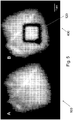
- Figure 5 shows the FWM signal obtained from a piece of carbon nanomaterial 100 before processing, in the left part, as indicated with the letter "A”.
- Figure 5 further shows the FWM signal obtained from a processed piece of carbon nanomaterial 400, i.e. after processing, in the right part, as indicated with the letter "B”.
- the FWM signal decreases upon oxidation providing contrast between oxidized and non-oxidized areas. Since the level of oxidation correlates with electrical properties and FWM signal, the latter can be used to monitor change in electrical properties.
- the FWM signal obtained from the processed piece of carbon nanomaterial 400 ( Fig. 5 , B) clearly shows a dark rectangle. This indicates that an oxidized rectangular area has been patterned onto a piece of carbon nanomaterial.
- the carbon nanomaterial of Fig. 5 is monolayer graphene. In this way, a rectangle with electrical properties different from that of a base has been patterned.
- the bang gap of the patterned region (first area 120) may be in the ranges defined for either the first area 120 or the second area 130, as discussed above.
- the processed piece of carbon nanomaterial 400 can be used to form an electronic device.
- the processed piece of carbon nanomaterial 400 is electrically coupled with another object.
- the other object may be an electrical conductor, an electrical semiconductor, or an electrical insulator.
- the other object may be a metallic electrical conductor.
- the base 115 can form a conductor
- the first area 120 can form a semiconductor
- the second area 130 can from an insulator. Therefore, a processed piece of carbon nanomaterial 400 having a semiconducting first area 120 in between two conducting base areas 115 can act as a transistor, such as a field effect transistor (FET).
- FET field effect transistor
- the second area 130 can be used to electrically isolate the first area 120 from a conductor; whereby the conductor can be used to produce an electric field into the first area.
- Figure 4 shows an example of such a processed piece of carbon nanomaterial 400.
- the base 115 comprises four base areas 115a, 115b, 115c, and 115d.
- the base areas 115a and 115b are electrically coupled to a semiconducting first area 120.
- the semiconducting area is made as has been described above for the first area 120.
- the processed piece of carbon nanomaterial 400 comprises insulating second areas 130.
- an insulating area, or insulating areas 130 is/are used to electrically insulate, from each other, such conductive areas 115a and 115b that are electrically connected to the semiconducting area 120.
- the insulating areas 130 are used to isolate the conductive areas 115a and 115b also from the other base areas 115c and 115d in order not to form an electric short circuit between the areas 115a and 115b that are electrically coupled to the semiconducting area 120.
- the conductive areas 115c and/or 115d can be used to generate an electric field to the semiconducting first area 120.
- Such a transistor comprises
- the means for affecting the electrical conductivity may comprise e.g. an electrical conductor (e.g. 115c and/or 115d) electrically insulated, e.g. by the second area 130, from the first area 120, thereby arranged to generate an electric field into the first area 120.
- an electrical conductor e.g. 115c and/or 115d
Landscapes
- Chemical & Material Sciences (AREA)
- Engineering & Computer Science (AREA)
- Nanotechnology (AREA)
- Materials Engineering (AREA)
- Organic Chemistry (AREA)
- Inorganic Chemistry (AREA)
- Manufacturing & Machinery (AREA)
- Crystallography & Structural Chemistry (AREA)
- Physics & Mathematics (AREA)
- Electromagnetism (AREA)
- Optics & Photonics (AREA)
- Condensed Matter Physics & Semiconductors (AREA)
- General Physics & Mathematics (AREA)
- Carbon And Carbon Compounds (AREA)
- Thin Film Transistor (AREA)
Description
- The invention relates to a method for processing carbon nanomaterial.
- Carbon nano materials and graphene in particular are envisioned to be the key materials for future electronics, photonics and related technological areas. Graphene is a two-dimensional material consisting of hexagonal aromatic carbon network. It is ultrathin having a thickness of minimally only one atomic layer and it has excellent electronic properties, including conductivity, making it a potential material to be used in flexible, transparent thin electronic devices.
- The problem with pristine graphene is that it has no band gap and thus it is not suitable for electronics as such. What is needed is patterning of graphene with functionalities that allow opening of a band gap and tuning of it and other electrical properties. In this regard, several strategies are being developed. One possibility is to cut graphene into narrow ribbons which have band gap due to quantum confinement and edge effects. Another possibility is to use template growth of graphene nanoribbons. However, it is very difficult and expensive to control graphene ribbons to the required degree of precision.
- Laser ablation has been used for making narrow nanoribbons and for patterning graphene and for pattern transfer. In these methods, pulsed lasers were used for cutting graphene via ablation or burning. The processes could be locally controlled by focusing the laser beam to a small diameter. Patterns could be made by moving the sample under laser illumination. The key common factor in these methods is that in all of them laser is used to remove material from graphene sheet. Thus, these methods cannot be used for controlling electrical properties of patterned areas.
- In this field, the publication
US2009/0311489 discloses a patterning method for a carbon nanotube (CNT) layer. The method is based on focusing a laser beam on the layer and moving the sample relative to the laser beam. The effect of the laser beam is to remove CNT material by ablation or burning, thus this method can only remove material but not change its electrical properties. Thus, carbon nanomaterial with areas of different electrical properties cannot be obtained. - Another strategy involves patterning of graphene oxide (GO). GO is a form of graphene which contains chemical groups with oxygen, typically C=O, O-H and C-O-C groups. GO is made from graphite. GO is insulator and it has to be reduced to reduced GO (RGO) in order to make it conductive to some extent. However, RGO is not the same material as pristine graphene and it does not have as good electrical properties as pristine graphene. Thus, these methods suffice from obtaining carbon nanomaterial with extremely good conductivity and low band gap. Thus, RGO does not have the excellent electrical properties of pristine graphene, e.g. because of the oxidation-reduction process of graphite. Still further, if the oxidation or reduction is made using wet chemistry, the graphite for GO may become contaminated, which further worsens the electrical properties of RGO.
- In addition, some of these methods require using equipment with reasonable high investment costs. Still further, the spatial accuracy of some methods is not satisfactory for future electronics requiring a line width in the 500 nm region and below.
- Method of locally oxidizing carbon nanomaterials are described in
US 2014/094021 A1 and FETHULLAH GÜNES ET AL: "UV-LIGHT-ASSISTED OXIDATIVE sp 3 HYBRIDIZATION OF GRAPHENE",NANO, vol. 06, no. 05, 2011, pages 409-418. - It has been found that carbon nanomaterials can be locally patterned by means of oxidation induced by electromagnetic radiation, such as visible light, or infrared radiation. The method is applicable to various types of carbon nanomaterials, however, in particular to material comprising graphene. The method comprises exposing carbon nanomaterial to light in an environment comprising oxygen. As a result, on one hand, the material becomes locally oxidized in a controlled manner. On the other hand, the oxidation and in particular the degree of oxidation affects the local properties (such as an electrical property, such as electrical conductivity and/or band gap) of the nanomaterial. Depending on the process parameters, different areas can be oxidized in different ways, resulting in carbon nanomaterial with at least three types of regions: un-processed, and two areas that have been processed differently. In the corresponding regions, the carbon nanomaterial has different properties.
- The method of the invention is as defined in claim 1.
- According to the invention, the carbon nanomaterial comprises, preferably consists of,
- a monolayer, e.g. a planar or bent monolayer, of graphene, optionally at most partly oxidized, or
- multilayer graphene, e.g. planar or bent, comprising a number of graphene monolayers, wherein the number is at most 30, optionally chemically treated on at least a surface.
- The method is easy to control. Thereby both insulating and semiconductive regions can be patterned onto a piece of conducting carbon nanomaterial resulting in a processed piece on nanomaterial having conductive, semiconductive, and insulating areas. Alternatively, some other property of the material (than the conductance) can be affected. The other property may be an electrical property or another property, such as luminescence.
-
- Fig. 1a
- shows locally exposing a first area of a piece of carbon nanomaterial to light,
- Fig. 1b
- shows locally exposing a second area of a piece of carbon nanomaterial to light after the first area has been exposed and oxidized,
- Fig. 2a
- shows an example of a graphene monolayer as seen from top,
- Fig. 2b
- shows an example of multilayer graphene in an exploded perspective view,
- Fig. 2c
- shows examples of carbon nanotubes,
- Fig. 2d
- shows an example of a network of carbon nanotubes,
- Fig. 3a
- shows a way of locally exposing a part of a piece of carbon nanomaterial to light, and
- Fig. 3b
- shows a way of locally exposing a part of a piece of carbon nanomaterial to light,
- Fig. 4
- shows a processed piece of carbon nanomaterial and different areas therein, and
- Fig. 5
- shows a piece of carbon nanomaterial, as observed with four-wave mixing (FWM) microscopy, before (A) and after (B) patterning it with the presented method.
- Carbon nanomaterials are known to conduct heat and electricity very well because of exceptionally high carrier mobility. Thus, carbon nanomaterials are often seen as one of the best candidates for future electronics. To make functional devices from carbon nanomaterial, such as graphene, areas with different properties, such as electrical, mechanical, and/or optical properties, must be patterned onto the nanomaterial. In particular, to make functional electronic devices from carbon nanomaterial, such as graphene, areas with different electrical properties must be patterned onto the nanomaterial. These properties may be e.g.
- an electrical property, such as electrical conductivity or band gap,
- an optical property, such as luminescence, transmittance or reflectivity, or
- a mechanical property, such as elastic modulus or brittleness (often measured in terms of tensile strain at break).
- It has been found that some of these properties are affected by the degree of oxidation of the carbon material. The term "oxidation" refers to the reaction, wherein at least some of the carbon atoms of the carbon material react with oxygen in such a way that at least some of the oxidized carbon atoms still remain bonded with the other carbon atoms of the piece of carbon material. The degree of oxidation refers to the molar ratio of oxygen atoms to carbon atoms, later denoted by NO/NC. However, during oxidation, at least some carbon atoms may be removed from the piece of carbon nanomaterial. E.g. the material may be locally burned, whereby some carbon atoms of the carbon nanomaterial form gaseous carbon oxides, e.g. carbon monoxide (CO) or carbon dioxide (CO2).
- It has been found that carbon nanomaterials can be locally patterned by means of oxidation induced by electromagnetic radiation. This means that oxidation is induced locally at an area that is exposed to said electromagnetic radiation in an environment comprising oxygen. Moreover, it has been found that the degree of oxidation can be controlled by controlling at least one of (i) the properties of the radiation used for oxidation, (ii) the exposure time, and/or (iii) the oxygen content of the environment. As the level of oxidation is affected locally, also the other properties that depend thereon, are affected locally.
- According to the invention, the light-induced oxidation is due to two-photon or multiphoton induced oxidation. The light-induced oxidation is due to two-photon or multiphoton induced oxidation, wherein the photons are from the visible or near infrared wavelength region (i.e. from 400 nm to 1100 nm). The light-induced oxidation is due to two-photon or multiphoton induced oxidation, wherein the photons are from the visible wavelength region (i.e. from 400 nm to 700 nm). The light-induced oxidation is due to two-photon or multiphoton induced oxidation, wherein the photons are from the near infrared wavelength region (i.e. from 700 nm to 1100 nm). In addition or alternatively, and not forming part of the invention, the light-induced oxidation may be due to single-photon induced oxidation. The light-induced oxidation may be due to single-photon induced oxidation, wherein the photon is from the ultra violet wavelength region (i.e. from 250 nm to 400 nm). Other values of the different parameters will be discussed later.
- In general, photosensitive materials have been known for a long time. In the electronics manufacturing technology photosensitive materials are commonly used together with various passive masks, wherein the passive mask comprises areas that are transparent and other areas that are opaque, and the transparency of these areas cannot be actively controlled, e.g. by electrical means. By exposing the photosensitive material through the passive mask, an image can be patterned on e.g. a preform of a printed circuit board. After exposure, some exposed material may be e.g. washed away while the unexposed material remains on the preform (or vice versa). However, the sensitivity of carbon nanomaterials to light has not been known, or at least has not been utilized in the manufacture of electronic devices.
- Manufacturing such a passive mask is very expensive. Moreover the cost increases as the line width of the passive mask decreases. Thus, passive masks for future electronics with small line widths will be very expensive. In various embodiments of the method, a passive mask can totally be omitted. This is because the required intensities, in particular for two-photon or multiphoton oxidation, are high, whereby a laser is used to generate light. A laser produces a collimated beam, optionally a beam comprising at least one pulse. Therefore, laser light can be used to only locally expose the carbon nanomaterial even without a passive mask.
- With reference to
Fig. 1a , a piece ofcarbon nanomaterial 100 can be locally oxidized, i.e. patterned. The piece ofcarbon nanomaterial 100 has a length L, a width W, and a thickness T, such that the length L is greater than or equal to the thickness T, the width W is greater than or equal to the thickness T. Each of the directions of length L, width W, and thickness T are perpendicular to the other two directions. As for the term "nanomaterial", the thickness is at most 50 nm. The thickness may be at most 10 nm or at most 5 nm. - The term "carbon nanomaterial" may also refer to an object that is obtainable, by bending or rolling, from a sample of carbon nanomaterial having a length L, a width W, and a thickness T. Also here the length L is greater than or equal to the thickness T, the width W is greater than or equal to the thickness T. Each of the directions of length L, width W, and thickness T are perpendicular to the other two directions. As for the term "nanomaterial", the thickness of the sample of carbon nanomaterial, from which the piece of carbon nanomaterial is obtainable, is at most 50 nm. The thickness T of the sample of carbon nanomaterial, used to form the piece of
carbon nanomaterial 100, may alternatively be e.g. at most 10 nm or at most 5 nm. - The small thickness is in many ways beneficial in particular for future electronics devices. Thin carbon nanomaterials are very flexible, whereby the shape of the material can be easily deformed e.g. by bending or rolling. Moreover, the thin carbon nanomaterial may be practically transparent, whereby electronic devices invisible to the naked eye can be manufactured. It has been observed, that by selecting the process parameters appropriately (see below), the light-induced oxidation can be used also for practically transparent carbon nanomaterials. Naturally, the transparency of the carbon nanomaterial can be slightly less than one, since the light interacts with the carbon nanomaterial. The transparency of a piece of
carbon nanomaterial 100, for the visible wavelength range (from 400 nm to 700 nm) can be e.g. at least 75% or at least 90 %. - The piece of
carbon nanomaterial 100 comprises aregion 110, wherein the region comprises at least 80 mol-% carbon atoms. Theregion 110 may comprise at least 90 mol-% carbon atoms or at least 95 mol-% carbon atoms. Moreover, initially the piece ofcarbon nanomaterial 100 may have uniform properties. Thus, the piece ofcarbon nanomaterial 100 may comprise at least 80 mol-% carbon atoms, at least 90 mol-% carbon atoms or at least 95 mol-% carbon atoms. Theregion 110 may have the same size as the piece ofcarbon nanomaterial 100, or it may be smaller. - Initially, the
region 110 may be un-oxidized or oxidized to some degree. Therefore, in theregion 110, the molar ratio of oxygen to carbon has a base value that is equal to or greater than zero. This molar ratio in theregion 110 is defined as NO/NC, wherein NO is the number of oxygen atoms in the region 110 (optionally zero) and NC is the number of carbon atoms in the region 110 (greater than zero). The base value is thus the ratio NO/NC in theregion 110; this will be denoted by NO/NC|110. - With the method, a
first area 120 will be oxidized. Theregion 110 comprises thefirst area 120. Thefirst area 120 is smaller than theregion 110. Thereby theregion 110 and thefirst area 120 define a base 115 that is comprised by the difference of theregion 110 and thefirst area 120. The difference of theregion 110 and thefirst area 120 is the set of points of theregion 110 that are not comprised by thefirst area 120. In the set theory this is often denoted by the sign "-". The difference of theregion 110 and thefirst area 120 can thus be denoted e.g. by "110-120". The difference of the region and the first area, 110-120, is a non-empty set, because thefirst area 120 is smaller than theregion 110. Thebase 115 is comprised by this difference; seefig 1a . - The method, i.e. a first embodiment of the method, comprises - generating a first
light pulse sequence 150 with first light pulse sequence property values, the firstlight pulse sequence 150 comprising at least one light pulse. - The first light pulse sequence property values include e.g. intensity, wavelength, duration, and number of light pulses in the first sequence of light pulses.
- The method further comprises
- exposing the
first area 120 to said firstlight pulse sequence 150 in afirst process environment 155 having a first oxygen content. - The method relates to patterning the carbon nanomaterial, the patterning being inherently a local process, whereby not all of the piece of
carbon nanomaterial 100 is treated by the method. Thus, the method comprises - exposing the
first area 120 to said firstlight pulse sequence 150 without exposing at least part of the base 115 to said firstlight pulse sequence 150. - It has been observed, that by the presence of oxygen, light-induced oxidation takes place in the
first area 120, but not in thebase 115. By said exposing, and because the first process environment has the first oxygen content, the method comprises - oxidizing locally, in the
first area 120, at least some carbon atoms of the piece ofcarbon nanomaterial 100. - It has furthermore been observed, that if the intensity of light is exceptionally high, some of the carbon nanomaterial can be removed from the piece of
carbon nanomaterial 100. However, to make a functioning device from carbon nanomaterial, only minor amounts of carbon, if any, should be removed by said exposing. Therefore the method comprises - oxidizing locally, in the
first area 120, at least some carbon atoms of the piece ofcarbon nanomaterial 100 in such a way that - at most 10 % of the carbon atoms of the
first area 120 are removed from thefirst area 120. - Moreover, as the light-induced oxidation takes place in the
first area 120, after said exposing thefirst area 120 to said firstlight pulse sequence 150, in thefirst area 120, the molar ratio of oxygen to carbon atoms has a first value, wherein the first value is greater than the base value. Thefirst area 120 comprises a number NO|120 of oxygen atoms and a number NC|120 of carbon atoms. The molar ratio of oxygen to carbon atoms, (NO|120)/(NC|120), in thefirst area 120, will be denoted by NO/NC|120. Since oxidation has taken place, NO/NC|120 > NO/NC|110. - Because at least a part of the
base 115 is not exposed, the base comprises a part, wherein the level of oxidation of the part of thebase 115 is not affected. Since in this way oxidation occurs only locally, the method comprises - patterning thefirst area 120 of the piece ofcarbon nanomaterial 110. - It has been found that the method is suitable for patterning e.g. graphene. Within this description, the term "graphene" is used for planar, bent or rolled graphene sample; however, a graphene sample that is rolled to form a closed tube is called a nanotube. The carbon nanotube is either open or closed from its ends; however the surface of the nanotube is closed. In contrast, a carbon nanoscroll is a rolled graphene sample with a spiral (open) cross section. In contrast to nanotubes, the term "graphene" may refer to planar, bent, or rolled open graphene sample.
- According to the invention, the piece of
carbon nanomaterial 100 comprises, or preferably consist of - a monolayer of graphene, e.g. planar or bent, and optionally at most partly oxidized, or
- multilayer graphene, e.g. planar or bent, comprising a number of graphene monolayers, wherein the number is at most 30, optionally chemically treated on at least a surface.
- It has also been found that the degree of light-induced oxidation depends on the parameters used for oxidation. Moreover, it has been found that it is possible to pattern a
second area 130 of the same piece ofcarbon nanomaterial 100 in such a way that the in thesecond area 130, the molar ratio of oxygen to carbon atoms has a second value NO/NC|130, the second value being greater than the base value, i.e. NO/NC|130 > NO/NC|110, and different from the first value, i.e. NO/NC|130 ≠ NO/NC|120. - A second embodiment of the method comprises all the steps of the first embodiment. In particular, since the first embodiment comprises exposing the
first area 120, the first (and the second) embodiments comprise - using a first set of values of process parameters to oxidize the
first area 120, wherein - the first set of values of process parameters comprises the first light pulse sequence property values and the first oxygen content.
- The first set of values of process parameters may comprise e.g. the value of the intensity, the value of the wavelength(s), the value of the duration, and value of the number of light pulses in the first sequence of
light pulses 150; in addition to the value of the first oxygen content of thefirst process environment 155. - With reference to
Fig. 1b , the piece ofcarbon nanomaterial 100 further comprises asecond area 130. As will be discussed, in a second embodiment, thesecond area 130 is exposed to a secondlight pulse sequence 160. Thefirst area 120 is also shown inFig. 1b . Thesecond area 130 may be comprised by thefirst area 120. Thesecond area 130 does not comprise thewhole base 115, which base 115 is not exposed to the firstlight pulse sequence 150 by the first embodiment of the method. In other words, the difference of thesecond area 130 and thebase 115 is a non-empty set. Thus at least a part of the base 115 remains unexposed (to both thelight pulse sequences 150 and 160) also in the second embodiment. - The second embodiment comprises
- changing at least one value of a process parameter of the first set of values of process parameters thereby generating a second set of values of process parameters, wherein at least a value of a process parameter in the first set of values of process parameters is different from the value of the process parameter in the second set of values of process parameters.
- Thus, the second embodiment may comprise changing, when changing the light pulse sequence that exposes the piece of carbon nanomaterial, i.e. the exposing light pulse, from the
first sequence 150 to thesecond sequence 160, at least one of - the intensity of light of a light pulse of the exposing light pulse sequence (150, 160),
- the duration of a light pulse of the exposing light pulse sequence (150, 160),
- the number of light pulses in the exposing light pulse sequence (150, 160),
- the exposure time used for exposing the area (120, 130),
- the repetition rate of the light pulses in the light pulse sequence (150, 160),
- the oxygen content of the environment wherein the carbon nanomaterial is oxidized, or
- the environment.
- The second embodiment further comprises
- generating a second
light pulse sequence 160 with second light pulse sequence property values, the second light pulse sequence property values comprised by the second set of values of process parameters, the secondlight pulse sequence 160 comprising at least one light pulse. - The second embodiment further comprises
- exposing the
second area 130 to said secondlight pulse sequence 160 in (a) theprocess environment 155 having a second oxygen content or (b) anotherprocess environment 165 having a second oxygen content, the second oxygen content comprised by the second set of values of process parameters. - For example, if the first exposure is made in a second, different,
environment 165, the second exposure can be made in thesecond environment 165 having a different oxygen content. The piece ofcarbon nanomaterial 100 can be moved from thefirst environment 155 to thesecond environment 165. However, the oxygen contents of the first and the second environments may be constants in time. - Alternatively, the same environment (i.e. location) can be used for both exposures, in such a way that the oxygen content is changed in between the first exposure and the second exposure. Alternatively, the same environment can be used for both exposures, in such a way that the oxygen content is not changed in between the first exposure and the second exposure; instead
light pulse sequences - In particular, the second embodiment comprises exposing the
second area 130 to said secondlight pulse sequence 160 without exposing at least part of the part the base 115 that has not been exposed to the firstlight pulse sequence 150 to said secondlight pulse sequence 160. Thus, at least part of thebase 115 is not exposed to either the firstlight pulse sequence 150 or the secondlight pulse sequence 160. - As at least one value of a process parameter is changed, at least a value of the process parameter used to expose the
second area 130 to the secondlight pulse sequence 160 is different from the value of the corresponding process parameter used to expose thefirst area 120 to the firstlight pulse sequence 150, whereby thesecond area 130 is oxidized in a different way than thefirst area 120. Moreover at least a part of thebase 115 is not oxidized or not further oxidized. Thus, the method comprises - oxidizing locally, in the
second area 130, at least some carbon atoms of the piece ofcarbon nanomaterial 100. - Also in the second embodiment, only a little material, if any, is removed by said exposing. Thus, the second embodiment comprises
- oxidizing locally, in the
second area 130, at least some carbon atoms of the piece ofcarbon nanomaterial 100 in such a way that at most 10 % of the carbon atoms of thesecond area 130 are removed from thesecond area 130. - Because the
second area 130 is oxidized, after said exposing thesecond area 130 to said secondlight pulse sequence 160, in thesecond area 130, the molar ratio of oxygen to carbon atoms has a second value NO/NC|130, the second value being greater than the base value, i.e. NO/NC|130 > NO/NC|110. - Because the
second area 130 is oxidized using different process parameters for the light-induced oxidation than for the light-induced oxidation of thefirst area 120, after said exposing thesecond area 130 to said secondlight pulse sequence 160, in thesecond area 130, the molar ratio of oxygen to carbon atoms has a second value NO/NC|130, the second value being different from the first value, i.e. NO/NC|130 ≠ NO/NC|120. - As discussed, the oxidation affects e.g. the electrical properties of the piece of
carbon nanomaterial 100 locally. An example of such an electrical property is the (local) band gap of the material. Band gap, in general, is small for electrical conductors, and large for electrical insulators. - In an embodiment of the method, the piece of
carbon nanomaterial 100 is initially not oxidized. Thus, also after processing, at least part of thebase 115 is an electric conductor. Therefore, in this embodiment, the band gap of at least that part of thebase 115 is at most 0.01 eV, such as zero eV. In a corresponding way, in the processed piece ofnanomaterial 400, obtained by processing the piece ofcarbon nanomaterial 100, the band gap of the part of the base is at most 0.01 eV, such as zero eV. In a preferred embodiment, the piece of carbon nanomaterial comprises graphene and the band bap of the unprocessed part of thebase 115 is within these values. - As a comparative example, the band gap of reduced graphene oxide (RGO) may be in the range from 0.02 eV to 2 eV. Therefore, such a processed piece of
carbon nanomaterial 400 suits electronics much better than a piece consisting of RGO or made from RGO. In a similar way, by applying the method to a piece of carbon nanomaterial having a base with band gap less than 0.02 eV will produce a processed piece ofcarbon nanomaterial 400 that is superior for purposes of electronics, as compared to devices based on RGO. Correspondingly, the part of thebase 115 of the processedpiece 400 could have a band gap less than 0.02 eV. - The piece of
carbon nanomaterial 100 may have initially been oxidized to some extent. Thus, the band gap of the base 115 may be also greater than 0.01 eV. According to the first embodiment of the method, the conductivity of thefirst area 120 of the piece ofnanomaterial 100 is decreased by said oxidation. Thus, in an embodiment, thefirst area 120 is oxidized in such a way that the band gap of thefirst area 120 is more than the bang gap of the aforementioned conductive part of thebase 115. More specifically, in an embodiment, - the
base 115 has a base band gap, - the
first area 120 is oxidized in such a way that the band gap in thefirst area 120 has a first band gap value, wherein - the first band gap value is more than the base band gap and
- the
second area 130 is oxidized in such a way that the band gap in thesecond area 130 has a value that is more than the first band gap value. - In addition, to make the
first area 120 semiconducting (i.e. not well conducting or well insulating), thefirst area 120 may be oxidized in such a way that the band gap of thefirst area 120 is more than 0.05 eV, such as at least 0.1 eV. Still further, to make thefirst area 120 semiconducting, thefirst area 120 may be oxidized in such a way that the band gap of thefirst area 120 is less than 3 eV, such as at most 2 eV. - Thus, in a corresponding processed piece of
carbon nanomaterial 400, thefirst area 120 of a processed piece ofcarbon nanomaterial 400 is (or has been) oxidized in such a way that the band gap of thefirst area 120 is - more than the bang gap of the part of the
base 115, optionally less than 3 eV and/or - more than 0.05 eV, such as at least 0.1 eV, optionally less than 3 eV.
- According to the second embodiment of the method, the conductivity of the
second area 130 of the piece ofnanomaterial 100 is decreased by said oxidation. The first andsecond areas second area 130 is oxidized more than thefirst area 120. Thesecond area 130 can be oxidized e.g. to form an electrically insulating area. Thus, in an embodiment, thesecond area 130 is oxidized in such a way that the band gap of thesecond area 130 is - more than the bang gap of the
first area 120, and/or - at least 3 eV.
- Thus, in an embodiment, the
second area 130 of a processed piece ofcarbon nanomaterial 400 is (or has been) oxidized in such a way that the band gap of thesecond area 130 is - more than the bang gap of the
first area 120, and/or - at least 3 eV.
- As discussed above, preferably laser light source(s) is/are used to generate a light pulse sequence (150 or 160) or the
light pulse sequences - According to the invention, the first light pulse sequence is generated using a laser, such that a light pulse of the first light pulse sequence comprises photons having a wavelength from 400 nm to 1100nm, thereby oxidizing locally, in the first area, at least some carbon atoms of the piece of carbon nanomaterial by two-photon or multiphoton oxidation.
- Thus, in an embodiment,
- the first
light pulse sequence 150 is generated using a first laser light source. The laser light source may be the light source 330 (seeFig. 3b ) or the light source 180 (seeFig. 3a ). - In an embodiment, wherein also the second
light pulse sequence 160 is generated, - the second
light pulse sequence 160 is generated using a laser light source, such the first laser light source or another laser light source (seeFigs. 3a and 3b ). - The first (and optionally the other) laser light source is arranged to produce a light pulse sequence 150 (optionally also 160). Thus, preferably a pulse laser is used as the light source for generating a light pulse sequence (150, 160). The pulse laser light source is arranged to generate laser light pulses having a duration. The duration is preferably in the range of from 1 fs to 1 ps, such as from 10 fs to 200 fs, such as from 20 fs to 60 fs. This duration has been observed to provide good control of intensity and exposure time in view of oxidation. The number of light pulses in a light pulse sequence (150, 160) may be e.g. in the order of 106.
- As discussed above, and with reference to
Figs. 3a and 3b , when a laser light source is used, a mask is not required. Thus, in an embodiment, - the first
light pulse sequence 150 is conveyed from the first laser light source (180, 330) onto thefirst area 120 without penetrating a passive mask that comprises areas that are transparent and other areas that are opaque. In particular, in this embodiment, the firstlight pulse sequence 150 is not attenuated or blocked by an opaque area of the passive mask. Thus - the first
light pulse sequence 150 is conveyed from the first laser light source (180, 330) onto thefirst area 120 without being at least partly blocked by an opaque area of a passive mask, through which the firstlight pulse sequence 150 is arranged to run. - As for the term passive mask, the local transparency of the passive mask, i.e. the transparency of the transparent and opaque areas of the passive mask, cannot be electrically controlled.
- In an embodiment,
- the second
light pulse sequence 160 is conveyed from the first laser light source (180, 330) or another laser light source onto thesecond area 130 without penetrating a passive mask that comprises areas that are transparent and other areas that are opaque. For example, without being at least partly blocked by an opaque area of a passive mask, through which the secondlight pulse sequence 160 is arranged to run. - Naturally, a passive mask could be used for patterning. In a corresponding embodiment, at least part of the first
light pulse sequence 150 is arranged to run through a passive mask, such that at least part of the firstlight pulse sequence 150 is blocked by an opaque area of the passive mask. - It has been found that the degree of oxidation affects in particular the electrical conductivity of the piece of
carbon nanomaterial 100. The electrical conductivity, on the other hand, can be locally engineered to form a functional electronic device. For example, in a third embodiment, wherein the steps of the first embodiment are performed, - the
base 115 has a base electrical conductivity and - the
first area 120 is oxidized in such a way that the electrical conductivity of thefirst area 120 is less than the base electrical conductivity. - For example, the base 115 can form a conductor and the
first area 120 can form a semiconductor. The conductivity of semiconductors can be affected e.g. by an electric field. - In a corresponding way, in an embodiment,
- the
base 115 has a base band gap and - the
first area 120 is oxidized in such a way that the band gap in thefirst area 120 is more than the base band gap. - Moreover, in a fourth embodiment, wherein the steps of the second embodiment are performed,
- the
base 115 has a base electrical conductivity - the
first area 120 is oxidized in such a way that the electrical conductivity of thefirst area 120 has a first electrical conductivity, wherein - the first electrical conductivity is less than the base electrical conductivity and
- the
second area 130 is oxidized in such a way that the electrical conductivity of thesecond area 130 is less than the first electrical conductivity. - Several types of carbon nanomaterials can be patterned with various embodiments of the method.
-
Figs. 2a to 2c show examples of pieces of carbon nanomaterials. A piece ofcarbon nanomaterial 100 may comprise - a monolayer of graphene 210 (
Fig. 2a ), - multiple layers of graphene (
Fig. 2b ), i.e. multilayergraphene 220 comprising a number N ofgraphene monolayers 210, preferably at most 30 graphene monolayers, - a carbon nanotube 240 (
Fig. 2c ), such as a single wall carbon nanotube (SWCNT) - another carbon nanotube 240 (
Fig. 2c ), such as a multi wall carbon nanotube (MWCNT), and/or - a net of
carbon nanotubes 240 attached to each other (Fig. 2d ). The nanotubes may be attached from their ends or otherwise. -
Figure 2a shows agraphene monolayer 210, which is an example of a piece ofcarbon nanomaterial 100. Graphene is a two-dimensional material consisting of hexagonal aromatic carbon network. It is ultrathin having a thickness of minimally only one atomic layer and it has excellent electronic properties making it a potential material to be used in flexible, transparent thin electronic devices. The graphene layer may be supported on a support, such as a polymer support or a glass support. It may also be supported only from its boundaries e.g. by a metal support. Such a graphene layer may be also oxidized to some degree, i.e. some of the atoms of the lattice may form a bond with an oxygen atom. -
Figure 2b shows amultilayer graphene 220, i.e. a thin piece comprising several (i.e. N)graphene monolayers 210, such as at most 30 monolayers. InFig. 2b , the number N is three. The piece ofcarbon nanomaterial 100, i.e. themultilayer graphene 220, may be supported on a support, such as a polymer support or a glass support. It may also be supported only from its boundaries e.g. by a metal support. Such a piece of carbon nanomaterial may be also oxidized to some degree, i.e. some of the carbon atoms may form a bond with an oxygen atom. -
Figure 2c shows acarbon nanotube 240, another example of a piece ofcarbon nanomaterial 100. Carbon nanotubes (CNT) can be considered as tubes formed from rolled graphene. CNTs can be either single walled (SWCNT) or multiwalled (MWCNT). CNTs can be either metallic or semiconducting depending on how the graphene sheet is rolled into a tube. A carbon nanotube has a diameter, which equals to both the width and the thickness of the piece ofcarbon nanomaterial 100. The length of a carbon nanotube is typically many times the diameter. Thecarbon nanotube 240 may be a single wall nanotube (SWCNT) or a multi wall nanotube (MWCNT), as illustrated inFig. 2c . - Thin films can be made from CNTs where a network of CNTs form a thin layer of interconnected tubes. CNT films can be used as (semi)transparent materials in electronic and sensor applications.
Figure 2d shows a network ofcarbon nanotubes 240, another example of a piece ofcarbon nanomaterial 100. Thecarbon nanotubes 240 may comprise single wall nanotubes (SWCNT) and/or multi wall nanotubes (MWCNT). The nanotubes are attached to each other. The nanotubes may be attached to each other from their ends or otherwise. - According to the invention, the
piece carbon nanomaterial 100 comprises, preferably consists of, - a monolayer of
graphene 210, - a monolayer of at least part oxidized graphene,
-
multilayer graphene 220 comprising a number ofgraphene monolayers 210, wherein the number is at most 30, - surface treated multilayer graphene comprising a number of graphene monolayers, wherein the number is at most 30, having been treated chemically from at least one surface.
- The carbon nanomaterial can comprise:
-
multilayer graphene 220 comprising a number ofgraphene monolayers 210, wherein the number is at most 10, and - surface treated multilayer graphene comprising a number of graphene monolayers, wherein the number is at most 10, having been treated chemically from at least one surface.
- Furthermore, the piece of carbon nanomaterial can be supported on a support, optionally from only its boundaries. The support may comprise e.g. less than 80 mol-% carbon atoms.
- The first
light pulse sequence 150 comprises a light pulse. The light pulses of the firstlight pulse sequence 150 are generated using at least one laser. Also, further lasers can be used to increase the intensity and/or to apply many different wavelengths to thefirst area 120. This applies as well to the secondlight pulse sequence 160 used in the second embodiment to expose thesecond area 130. - As for the wavelength, in the first or the second embodiment, the properties of the first
light pulse sequence 150 are selected such that - a light pulse of the first
light pulse sequence 150 comprises photons having a wavelength from 400 nm to 1100 nm. - In the second embodiment, the properties of the second
light pulse sequence 160 may be selected such that - a light pulse of the second
light pulse sequence 160 comprises photons having a wavelength from 250 nm to 1100 nm. - These wavelengths have been observed to effectively oxidize the piece of
carbon nanomaterial 100. - As for the intensity of the light of the first
light pulse sequence 150, in the first or the second embodiment, - a light pulse of the first
light pulse sequence 150 has an intensity from 109 W/(cm)2 to 1014 W/(cm)2; such as from 1010 W/(cm)2 to 1013 W/(cm)2, e.g. from 7×10¹⁰ W/(cm)2 to 7×10¹¹ W/(cm)2 - In the second embodiment,
- a light pulse of the second
light pulse sequence 160 has an intensity from 109 W/(cm)2 to 1014 W/(cm)2; such as from 1011 W/(cm)2 to 1013 W/(cm)2, e.g. from 7×10¹⁰ W/(cm)2 to 7×10¹¹ W/(cm)2 - These values have been found to be sufficiently high for local oxidation. These values have been found to be sufficiently high for local oxidation using multiphoton oxidation. These values have been found to be sufficiently low for preventing excessive removal of carbon material from the
first area 120, and optionally from thesecond area 130. - In particular, the intensity can be selected such that the intensity of all light pulses of the first
light pulse sequence 150 are below an ablation threshold. The ablation threshold is herein defined as the minimum intensity required to induce separation of carbon atoms from the piece ofcarbon nanomaterial 100 due to incident intense irradiation. The separated carbon atoms may form gaseous carbon oxide, such as carbon monoxide (CO) or carbon dioxide (CO2). This threshold may depend on the initial degree of oxidation, i.e. the base value NO/NC|110 (see above) and/or on the oxygen content of the environment (i.e. the first or the second oxygen content). - Moreover, it has been observed that when the process involves multiphoton excitation, intensity needs to be carefully selected; on one hand to enable multiphoton excitation, and on the other hand to avoid ablation. Multiphoton excitation seems to be needed at least when visible or near infrared light (wavelength from 400 nm to 1100 nm) is used in the corresponding light pulse sequence (150, 160). The aforementioned intensities are suitable for multiphoton oxidation. Moreover, the aforementioned intensities may be suitable also for light pulses of different wavelengths.
- As for the oxygen content of the
first environment 155, wherein the piece of carbon nanomaterial is exposed to light, in the first or the second embodiment - the first oxygen content is at least 0.4 mol/m3.
- the second oxygen content is at least 0.4 mol/m3.
- Moreover, it seems that the oxidation rate is insensitive to oxygen content, when the oxygen content is more than about 10 mol/m3.
- These values have been found to be sufficiently high for local oxidation. These values have been found to be sufficiently low for preventing ignition of the piece of carbon nanomaterial, at least for some of the aforementioned intensities. In principle, the higher the oxygen content, the lower intensity and/or shorter exposure time may suffice.
- As for the exposure time, it has been found that within the aforementioned intensity range, an exposure time between 10 ms and 10 s, such as from 100 ms to 5 s, such as from 0.5 s to 2 s, e.g. about 1s, provides good oxidation results. A smaller exposure time can be used with higher intensity and vice versa.
- The exposure time herein is defined as the time of exposing the area(s) (120, 130) to the light pulse sequence. More precisely, the difference of the instances when the last light pulse stops illuminating and when the first pulse starts illuminating. The proper exposure time may depend on a repetition rate of the light pulses of the light pulse sequence (150, 160).
- The repetition rate for the light pulses of the light pulse sequence (150, 160) can be defined as the number of light pulses per unit time. Thus, the repetition rate is the inverse of the time difference between subsequent light pulses (in particular the time difference of the same part of the pulses). A repetition rate from 10 kHz to 10 MHz, such as from 100 kHz to 1 MHz, such as about 600 kHz was seen to provide good oxidation results.
- The total illumination time, which is the product of (a) the number of light pulses in the pulse sequence (
first sequence 150 or second sequence 160) during the exposure time and (b) the pulse duration, may be significantly less. E.g. for the exposure time 1 s, repetition rate 600 kHz, and pulse duration 40 fs, the total illumination time is only 24 ns. - With the aforementioned pulse duration and exposure time, the applicable number of light pulse may be in the range from 1×10³ to 1×10⁷, such as from 1×10⁴ to 3×10⁶, such as from 1×10⁵ to 1×10⁶, e.g. about 6×10⁵.
- Future electronic devices are likely to be small and to comprise multiple differently operating areas. Therefore, the method is preferably applied in such a way that the patterned area is small and/or it is accurately shaped. As the patterning is light-induced, the first
light pulse sequence 150, when hitting thefirst area 120, i.e. the exposed area, preferably has a small size. The size of the exposed area can be controlled e.g. by using focusing optics or using near field optics. These can be used in the first embodiment or the second embodiment. Moreover, focusing can be used for thefirst area 120, and near field optics for thesecond area 130, or vice versa. Naturally focusing or near field optics can be used for both first 120 and second 130 areas. -
Figure 3a shows an example of using focusingoptics 310 to collimate the light firstlight pulse sequence 150 onto thefirst area 120. Similar optics could be used to collimate the secondlight pulse sequence 160 onto thesecond area 130. The device ofFig. 3a comprises - a
light source 180 arranged to generate the firstlight pulse sequence 150. Thelight source 180 may be arranged to generate the secondlight pulse sequence 160. and - and focusing
optics 310 arranged to decrease the cross sectional area of a light pulse of the firstlight pulse sequence 150. - focusing the first
light pulse sequence 150 using focusingoptics 310 to decrease the cross sectional area of a light pulse of the firstlight pulse sequence 150. - The focusing
optics 310 may comprise alens 310. In the alternative or in addition, a reflective surface can be used to focus the light pulse sequence (first or second). As is clear fromFig. 3a , the cross sectional area of a light pulse of the firstlight pulse sequence 150 decreases after passing thelens 310. The pattern size achievable using the device ofFig. 3a is limited by the wavelength of the light of the light pulse sequence. Thus, to produce areas with small line width, light of short wavelength should be used. -
Figure 3b shows an example of using near field optics to expose thefirst area 120 or thesecond area 130.Figure 3b shows alight pulse source 330, arranged to generate the firstlight pulse sequence 150 and to guide the firstlight pulse sequence 150 into awaveguide 320.Figure 3b shows also thewaveguide 320, which is arranged close to the area (120, 130) of the piece ofcarbon nanomaterial 100 that is exposed to light. - In near field optics, the distance d between an end of the
waveguide 320 and the exposed area (120, 130) is less than the wavelength of the light used. Thus, in an embodiment - a light pulse sequence (i.e. the first
light pulse sequence 150 or the second light pulse sequence 160) comprises a light pulse or light pulses having a longest wavelength. - using a
waveguide 320 to guide a light pulse sequence (i.e. the firstlight pulse sequence 150 or the second light pulse sequence 160) from alight source 330 to an end of the waveguide, in such a way that - the closest distance d between the end of the waveguide and the piece of
carbon nanomaterial 100 is at most the longest wavelength. - The longest wavelength may be e.g. 1100 nm, 700 nm, 300 nm, or 250 nm. Thus, the distance d may be e.g. at most 1100 nm, at most 700 nm, at most 300 nm, or at most 250 nm.
- To control the patterning process, in particular the shape of the patterned
first area 120, a passive mask could be used, as discussed above, but such a passive mask is preferably not used. Alternatively, the shape of the patternedfirst area 120 can be controlled by moving the beam. Still further, the shape of the patternedfirst area 120 can be controlled by the shape and/or intensity profile of the firstlight pulse sequence 150 and/or the secondlight pulse sequence 160. - During the illumination of the area (120, 130), the exposed area (i.e. the area that is illuminated by the a
light pulse sequence 150, 160) can be moved with respect to the piece ofcarbon nanomaterial 100 in order to pattern oxidized patterns that extend within the carbon nanomaterial. E.g. the piece ofcarbon nanomaterial 100 can be moved with respect to fixed optics. E.g. the piece ofcarbon nanomaterial 100 can be fixed, and the exposed area can be moved by moving or turning the optics. The speed of the relative movement affects the exposure time. Thus, thefirst area 120 andsecond area 130 can be patterned in different ways also by varying the speed by which the illuminated area (120, 130) is arranged to move on the piece of carbon nanomaterial. - The shape and/or intensity profile of a light pulse sequence, such as the first 150 or the second 160, can also be controlled by a spatial light modulator (SLM). In this embodiment, the input laser beam is structured so that some spatial parts have of the light pulse sequence have higher intensity and other spatial parts have lower intensity. In this way, some parts of the piece of carbon nanomaterial are oxidized in a different way than other parts. In contrast to e.g. a lens, which also modifies the spatial profile of light, a spatial light modulator is an active component. A spatial light modulator can be electronically controlled.
- Therefore, by using the spatial light modulator, a light pulse sequence be modified to comprise spatially two parts: a first
light pulse sequence 150 and a secondlight pulse sequence 160. In this embodiment, the two light pulse sequences are simultaneously used to oxidize thefirst area 120 and thesecond area 130. Naturally, two different light sources could also be used to simultaneously oxidize the areas in different ways. - The spatial light modulator may comprise a polarizer and an electrically controllable liquid crystal unit. The liquid crystal unit is arranged to locally change the polarization of light propagating through the liquid crystal unit. The amount of change in the polarization can be controlled electrically and locally within the liquid crystal unit. In combination with the polarizer, the transparency of the spatial light modulator becomes spatially non-uniform, whereby the spatial light modulator can be used to pattern the piece of carbon nanomaterial. Moreover the spatial transparency of the spatial light modulator is electrically controllable. In this way, the spatial light modulator forms an active mask. In contrast to aforementioned passive mask, the local transparency of the active mask, i.e. the transparency of the transparent and opaque areas of the active mask, can be electrically controlled.
- Thus, an embodiment comprises modifying the spatial profile of a light pulse sequence using an active spatial light modulator. As an example, an embodiment comprises modifying the spatial profile of a light pulse of a light pulse sequence using an active spatial light modulator. The active spatial light modulator may be electrically controllable. The local transparency of the active spatial light modulator may be electrically controllable.
- After the piece of
carbon nanomaterial 100 has been processed, a processed piece ofcarbon nanomaterial 400 is obtained, a processed piece of carbon nanomaterial not forming part of the invention as such. - With reference to
Fig. 4 , a processed piece ofcarbon nanomaterial 400 has - a length L, a width W, and a thickness T, such that
- the length L is greater than or equal to the thickness T, the width W is greater than or equal to the thickness T, and the thickness T is at most 50 nm,
- each of the directions of length L, width W, and thickness T are perpendicular to the other two directions.
- However, in addition to the aforementioned oxidation process, the sample of carbon nanomaterial or the piece of
carbon nanomaterial 100 can be obtainable, e.g. by bending or rolling, from a sample of carbon nanomaterial having a length, a width, and a thickness wherein the length is greater than or equal to the thickness, the width is greater than or equal to the thickness, and the thickness is at most 50 nm. - The processed piece of
carbon nanomaterial 400 is planar (i.e. not bent or rolled), wherein the processed piece of carbon nanomaterial has the measures described above. - The processed piece of
carbon nanomaterial 400 comprises - at least 80 mol-% carbon atoms,
- a base 115 having a part, at least the part of the base 115 comprising carbon atoms and oxygen atoms in such a way that the molar ratio of oxygen to carbon, NO/NC, has a base value NO/NC|110 (cf. above, note this ratio is not affected by the method, as the part of the base is not exposed to light) that is equal to or greater than zero,
- a
first area 120 comprising carbon atoms and oxygen atoms in such a way that the molar ratio of oxygen to carbon in thefirst area 120 has a first value NO/NC|120 that is greater than the base value NO/NC|110, and - a
second area 130 comprising carbon atoms and oxygen atoms in such a way that the molar ratio of oxygen to carbon in thesecond area 130 has a second value NO/NC|130 that is greater than the base value NO/NC|110 and different from the first value NO/NC|120. - As the processed piece of
carbon nanomaterial 400 is the result of processing the piece ofcarbon nanomaterial 100 by the second embodiment of the method, the processed piece ofcarbon nanomaterial 400 may comprise - a monolayer of graphene or multilayer graphene comprising a number of graphene monolayers, such as at most 30 monolayers,
- a carbon nanotube, such as a single wall carbon nanotube (SWCNT) or a multi wall carbon nanotube (MWCNT), or
- a net of carbon nanotubes attached to each other e.g. from their ends.
- In particular the processed piece of
carbon nanomaterial 400 may comprise, or preferably consist of - a non-rolled monolayer of graphene, optionally at least partly oxidized, or
- non-rolled multilayer graphene comprising a number of graphene monolayers, wherein the number is at most 30, optionally chemically treated on at least a surface.
- The processed piece of
carbon nanomaterial 400 may be arranged on a support, such as a glass support or a polymer support. The processed piece ofcarbon nanomaterial 400 may be arranged to a support only from its boundaries, such as attached to a metal support limiting an aperture, the processed piece ofcarbon nanomaterial 400 being arranged on the aperture. The support may comprise e.g. less than 80 mol-% carbon atoms. - When the areas are patterned using light-induced oxidation, reasonably small areas can be accurately patterned. In an embodiment,
- the
first area 130 has a line width WL, a line length LL, and a line thickness TL, the line thickness TL being parallel to the thickness T of the processed piece ofcarbon nanomaterial 400, the direction of the line width WL being perpendicular to the direction of the line length LL and perpendicular to the direction of the line thickness TL, and the line width WL being at most the line length LL, wherein - the line width WL is adapted to be suitable for electronic devices.
- Here the line thickness TL is parallel to the thickness of a layer of the processed piece of
carbon nanomaterial 400. When the processed piece of carbon nanomaterial is planar or bent, the processedpiece 400 comprises only one such layer. Thus, the line thickness TL is parallel to the thickness of the processed piece ofcarbon nanomaterial 400 and the layer of the processed piece ofcarbon nanomaterial 400. However, when the processed piece of carbon nanomaterial is rolled from a layer of nanomaterial, the line thickness TL is parallel to the thickness of the layer of the processed piece ofcarbon nanomaterial 400. - For example, the line width WL is at most 1 mm, such as at most 10 µm, at most 700 nm or at most 300 nm. The line width WL can be decreased by using the collimation optics or near field techniques as discussed above.
- In a corresponding method, the piece of
carbon nanomaterial 100 is processed in such a way that these measures are achieved. - The line length LL can be increased by moving the point, wherein the (first or second) light pulse sequence illuminates the piece of carbon nanomaterial.
- As the processed piece of
carbon nanomaterial 400 may have been made by light-induced oxidation that has removed some carbon atoms, for example, - at least some carbon atoms has been removed from a processed area of the processed piece of
carbon nanotube 400, whereby - the
first area 120 or thesecond area 130 comprises a groove. - Moreover, the molar ratio of oxygen to carbon, in the processed region (i.e. the
first area 120 or the second area 130) comprising the groove, is higher than in thebase 115. - The properties of the piece of
nanomaterial 100 or the processed piece ofmaterial 400 can be analyzed e.g. by using four-wave mixing (FWM) microscopy. In this method, three laser fields with different frequencies interact through the nanomaterial's susceptibility to generate a signal at a fourth frequency. The four wavelengths can be chosen to all be in the visible range in such a way that the fourth wavelength can be optically separated from the other three. Thereafter, an optical microscope can be used to analyze the signal at the fourth wavelength. The FWM signal is sensitive in particular to electrical and vibrational properties of the nanomaterial. By tuning the incoming or emitted frequencies into an electronic resonance of the material, selected electronic excitations can be probed. In addition, electronically resonant excitation of the material is accompanied by an enhanced FWM response. In this way, the change in the electrical properties of the material, as obtained by the aforementioned embodiments, can be confirmed. An example of an application of the FWM is coherent anti-Stokes Raman scattering (CARS) imaging. Another example of the FWM method is stimulated Raman scattering (SRS). -
Figure 5 shows the FWM signal obtained from a piece ofcarbon nanomaterial 100 before processing, in the left part, as indicated with the letter "A".Figure 5 further shows the FWM signal obtained from a processed piece ofcarbon nanomaterial 400, i.e. after processing, in the right part, as indicated with the letter "B". The FWM signal decreases upon oxidation providing contrast between oxidized and non-oxidized areas. Since the level of oxidation correlates with electrical properties and FWM signal, the latter can be used to monitor change in electrical properties. - The FWM signal obtained from the processed piece of carbon nanomaterial 400 (
Fig. 5 , B) clearly shows a dark rectangle. This indicates that an oxidized rectangular area has been patterned onto a piece of carbon nanomaterial. The carbon nanomaterial ofFig. 5 is monolayer graphene. In this way, a rectangle with electrical properties different from that of a base has been patterned. For example, the bang gap of the patterned region (first area 120) may be in the ranges defined for either thefirst area 120 or thesecond area 130, as discussed above. - The processed piece of
carbon nanomaterial 400 can be used to form an electronic device. In an electronic device the processed piece ofcarbon nanomaterial 400 is electrically coupled with another object. The other object may be an electrical conductor, an electrical semiconductor, or an electrical insulator. The other object may be a metallic electrical conductor. - For example, the base 115 can form a conductor, the
first area 120 can form a semiconductor, and thesecond area 130 can from an insulator. Therefore, a processed piece ofcarbon nanomaterial 400 having a semiconductingfirst area 120 in between two conductingbase areas 115 can act as a transistor, such as a field effect transistor (FET). Thesecond area 130 can be used to electrically isolate thefirst area 120 from a conductor; whereby the conductor can be used to produce an electric field into the first area. -
Figure 4 shows an example of such a processed piece ofcarbon nanomaterial 400. In the Figure, thebase 115 comprises fourbase areas base areas first area 120. The semiconducting area is made as has been described above for thefirst area 120. Moreover, the processed piece ofcarbon nanomaterial 400 comprises insulatingsecond areas 130. - With reference to
Fig. 4 , an insulating area, or insulatingareas 130, is/are used to electrically insulate, from each other, suchconductive areas semiconducting area 120. - In
Fig. 4 , wherein thepiece 400 comprises furtherconductive base areas areas 130 are used to isolate theconductive areas other base areas areas semiconducting area 120. Theconductive areas 115c and/or 115d can be used to generate an electric field to the semiconductingfirst area 120. - Such a transistor comprises
- a processed piece of
carbon nanomaterial 400, and - means for affecting the electrical conductivity of the
first area 120. - The means for affecting the electrical conductivity may comprise e.g. an electrical conductor (e.g. 115c and/or 115d) electrically insulated, e.g. by the
second area 130, from thefirst area 120, thereby arranged to generate an electric field into thefirst area 120.
Claims (9)
- A method for patterning a piece of carbon nanomaterial (100), wherein- the piece of carbon nanomaterial (100) (i) has a length (L), a width (W), and a thickness (T) or (ii) is obtainable, e.g. by bending or rolling, from a sample of carbon nanomaterial having a length (L), a width (W), and a thickness (T), wherein- the length (L) is greater than or equal to the thickness (T), the width (W) is greater than or equal to the thickness (T), and the thickness (T) is at most 50 nm,- the carbon nanomaterial comprises (i) a monolayer of graphene, optionally at most partly oxidized, or (ii) multilayer graphene comprising a number of graphene monolayers, wherein the number is at most 30, optionally chemically treated on at least a surface- the piece of carbon nanomaterial (100) comprises a region (110), in which the molar ratio of oxygen to carbon has a base value that is equal to or greater than zero,- the region (110) of the piece of carbon nanomaterial (100) comprises at least 80 mol-% carbon atoms,- the region (110) comprises a first area (120) in such a way that the first area (120) is smaller than the region (110); whereby the region (110) and the first area (120) define a base (115) that is comprised by the difference of the region (110) and the first area (120); the method comprising- generating a first light pulse sequence (150) with first light pulse sequence property values, the first light pulse sequence (150) comprising at least one light pulse and- exposing the first area (120) to said first light pulse sequence (150) in a first process environment (155) having a first oxygen content, without exposing at least part of the base (115) to said first light pulse sequence (150);- generating the first light pulse sequence (150) using a laser, such that a light pulse of the first light pulse sequence (150) comprises photons having a wavelength from 400 nm to 1100 nm, thereby- oxidizing locally, in the first area (120), at least some carbon atoms of the piece of carbon nanomaterial (100) by two-photon or multiphoton oxidation in such a way that- at most 10 % of the carbon atoms of the first area (120) are removed from the first area (120) and- after said exposing the first area (120) to said first light pulse sequence (150), in the first area (120), the molar ratio of oxygen to carbon atoms has a first value, the first value being greater than the base value; thereby- patterning the first area (120) of the piece of carbon nanomaterial (100).
- The method of claim 1, wherein- the piece of carbon nanomaterial (100) further comprises a second area (130) and- by said exposing the first area (120), the method comprises using a first set of values of process parameters to oxidize the first area (120), wherein the first set of values of process parameters comprises the first light pulse sequence property values and the first oxygen content; the method further comprising- changing at least one value of a process parameter of the first set of values of process parameters thereby generating a second set of values of process parameters, wherein at least a value of a process parameter in the first set of values of process parameters is different from the value of the process parameter in the second set of values of process parameters,- generating a second light pulse sequence (160) with second light pulse sequence property values, the second light pulse sequence property values comprised by the second set of values of process parameters, the second light pulse sequence (160) comprising at least one light pulse, and- exposing the second area (130) to said second light pulse sequence (160) (a) in the process environment having a second oxygen content or (b) in another process environment having a second oxygen content, the second oxygen content comprised by the second set of values of process parameters; thereby- using the second set of values of process parameters to oxidize at least some carbon atoms locally in the second area (130) in such a way that- at most 10 % of the carbon atoms of the second area (130) are removed from the second area (130) and- after said exposing the second the area (130) to said second light pulse sequence (160), in the second area (130), the molar ratio of oxygen to carbon atoms has a second value, the second value being greater than the base value and different from the first value.
- The method of claim 1 or 2, wherein the carbon nanomaterial consists of- a carbon nanotube, such as a single wall carbon nanotube (SWCNT) or a multi wall carbon nanotube (MWCNT), or- a net of carbon nanotubes attached to each other e.g. from their ends; and- the method comprises patterning graphene.
- The method of the claim 1 or 2, wherein the carbon nanomaterial consists of- a monolayer of graphene, optionally at most partly oxidized, or- multilayer graphene comprising a number of graphene monolayers, wherein the number is at most 30, optionally chemically treated on at least a surface.
- The method of any of the claims 1 to 4, wherein- a light pulse of the first light pulse sequence (150) has an intensity from 109 W/(cm)2 to 1014W/(cm)2; such as from 7×10¹⁰ W/(cm)2 to 7×10¹¹ W/(cm)2.
- The method of any of the claims 1 to 5, wherein- the first oxygen content is at least 0.4 mol/m3, and optionally at most 100 mol/m3; such as from 0.4 mol/m3 to 40 mol/m3.
- The method of any of the claims 1 to 6, wherein- the band gap of at least part of base (115) is at most 0.01 eV and- the first area (120) is oxidized in such a way that the band gap of the first area (120) is more than 0.05 eV, such as at least 0.1 eV.
- The method of claim 7, wherein- the second area (130) is oxidized in such a way that the band gap of the second area (130) is more than the band gap of the first area (120) and, optionally, the band gap of the second area (130) is more than 2 eV, such as at least 3 eV.
- The method of any of the claims 1 to 8, wherein- the first area (120) has a line width (WL), a line length (LL), and a line thickness, the line width (WL) being perpendicular to the line length (LL) and perpendicular to the line thickness, and the line width (WL) being at most the line length (LL), wherein- the line width (WL) is adapted to be suitable for electronic devices.
Applications Claiming Priority (2)
| Application Number | Priority Date | Filing Date | Title |
|---|---|---|---|
| FI20145408A FI20145408A7 (en) | 2014-05-05 | 2014-05-05 | A method for patterning a piece of carbon nanomaterial and a processed piece of carbon nanomaterial |
| PCT/FI2015/050298 WO2015170005A1 (en) | 2014-05-05 | 2015-05-04 | A method for patterning a piece of carbon nanomaterial and a processed piece of carbon nanomaterial |
Publications (2)
| Publication Number | Publication Date |
|---|---|
| EP3140870A1 EP3140870A1 (en) | 2017-03-15 |
| EP3140870B1 true EP3140870B1 (en) | 2020-01-08 |
Family
ID=53177506
Family Applications (1)
| Application Number | Title | Priority Date | Filing Date |
|---|---|---|---|
| EP15722559.0A Active EP3140870B1 (en) | 2014-05-05 | 2015-05-04 | A method for patterning a piece of carbon nanomaterial |
Country Status (6)
| Country | Link |
|---|---|
| US (1) | US10475651B2 (en) |
| EP (1) | EP3140870B1 (en) |
| KR (1) | KR102190402B1 (en) |
| ES (1) | ES2784248T3 (en) |
| FI (1) | FI20145408A7 (en) |
| WO (1) | WO2015170005A1 (en) |
Family Cites Families (9)
| Publication number | Priority date | Publication date | Assignee | Title |
|---|---|---|---|---|
| JP3851276B2 (en) | 2003-01-06 | 2006-11-29 | 独立行政法人科学技術振興機構 | Structure selection method of carbon nanotubes by light irradiation |
| JP3781732B2 (en) * | 2003-03-20 | 2006-05-31 | 株式会社東芝 | Carbon nanotube manufacturing method, semiconductor device manufacturing method using carbon nanotube, and carbon nanotube manufacturing apparatus |
| US20100025222A1 (en) | 2006-11-17 | 2010-02-04 | Nec Corporation | Method of forming pore in graphitic-carbon nanomaterial and method of introducing oxygen-containing group into pore |
| US8540922B2 (en) | 2007-08-27 | 2013-09-24 | Hewlett-Packard Development Company, L.P. | Laser patterning of a carbon nanotube layer |
| JP2011192667A (en) * | 2010-03-11 | 2011-09-29 | Toshiba Corp | Transistor and method of manufacturing the same |
| US20120068161A1 (en) * | 2010-09-16 | 2012-03-22 | Lee Keon-Jae | Method for forming graphene using laser beam, graphene semiconductor manufactured by the same, and graphene transistor having graphene semiconductor |
| US8609458B2 (en) | 2010-12-10 | 2013-12-17 | California Institute Of Technology | Method for producing graphene oxide with tunable gap |
| US9196766B1 (en) * | 2012-04-25 | 2015-11-24 | Magnolia Optical Technologies, Inc. | Thermal detectors using graphene and oxides of graphene and methods of making the same |
| KR101398881B1 (en) * | 2012-07-12 | 2014-06-02 | 주식회사 인피니트헬스케어 | Radiation treatment planning apparatus and method thereof |
-
2014
- 2014-05-05 FI FI20145408A patent/FI20145408A7/en not_active Application Discontinuation
-
2015
- 2015-05-04 US US15/307,176 patent/US10475651B2/en active Active
- 2015-05-04 WO PCT/FI2015/050298 patent/WO2015170005A1/en not_active Ceased
- 2015-05-04 ES ES15722559T patent/ES2784248T3/en active Active
- 2015-05-04 EP EP15722559.0A patent/EP3140870B1/en active Active
- 2015-05-04 KR KR1020167030843A patent/KR102190402B1/en active Active
Non-Patent Citations (1)
| Title |
|---|
| None * |
Also Published As
| Publication number | Publication date |
|---|---|
| WO2015170005A1 (en) | 2015-11-12 |
| US20170207391A1 (en) | 2017-07-20 |
| EP3140870A1 (en) | 2017-03-15 |
| KR20170008214A (en) | 2017-01-23 |
| ES2784248T3 (en) | 2020-09-23 |
| KR102190402B1 (en) | 2020-12-14 |
| FI20145408A7 (en) | 2015-11-06 |
| US10475651B2 (en) | 2019-11-12 |
Similar Documents
| Publication | Publication Date | Title |
|---|---|---|
| Maggiolini et al. | Strongly enhanced light–matter coupling of monolayer WS2 from a bound state in the continuum | |
| Piazza et al. | Simultaneous observation of the quantization and the interference pattern of a plasmonic near-field | |
| Proscia et al. | Near-deterministic activation of room-temperature quantum emitters in hexagonal boron nitride | |
| Geng et al. | Surface plasmons interference nanogratings: wafer-scale laser direct structuring in seconds | |
| Han et al. | Lasing at topological edge states in a photonic crystal L3 nanocavity dimer array | |
| Guan et al. | Far-field femtosecond laser-driven λ/73 super-resolution fabrication of 2D van der Waals NbOI2 nanostructures in ambient air | |
| Sidiropoulos et al. | Ultrafast plasmonic nanowire lasers near the surface plasmon frequency | |
| Low et al. | Laser-induced reduced-graphene-oxide micro-optics patterned by femtosecond laser direct writing | |
| Engel et al. | Light–matter interaction in a microcavity-controlled graphene transistor | |
| Öktem et al. | Nonlinear laser lithography for indefinitely large-area nanostructuring with femtosecond pulses | |
| Lee et al. | Quantum plasmonics: energy transport through plasmonic gap | |
| Hong et al. | Dielectric constant engineering of single-walled carbon nanotube films for metamaterials and plasmonic devices | |
| Kim et al. | Ambipolar charge-transfer graphene plasmonic cavities | |
| Mauclair et al. | Control of ultrafast laser-induced bulk nanogratings in fused silica via pulse time envelopes | |
| He et al. | Sub-diffraction limited writing based on laser induced periodic surface structures (LIPSS) | |
| Xia et al. | Localized plasmonic field enhancement in shaped graphene nanoribbons | |
| Machida et al. | Shrinkable silver diffraction grating fabricated inside a hydrogel using 522-nm femtosecond laser | |
| Solomon et al. | Ultrafast laser ablation, intrinsic threshold, and nanopatterning of monolayer molybdenum disulfide | |
| JP5867439B2 (en) | Grid polarizing element and optical alignment apparatus | |
| Vasquez et al. | Micro-structuring, ablation, and defect generation in graphene with femtosecond pulses | |
| Paz-Buclatin et al. | Circularly symmetric nanopores in 3D femtosecond laser nanolithography with burst control and the role of energy dose | |
| Torun et al. | Ultrafast laser direct-writing of self-organized microstructures in Ge-Sb-S chalcogenide glass | |
| Nicoletti et al. | Generation of λ/12 nanowires in chalcogenide glasses | |
| US10475651B2 (en) | Method for patterning a piece of carbon nanomaterial and a processed piece of carbon nanomaterial | |
| Mitchell et al. | Sub-diffraction laser synthesis of silicon nanowires |
Legal Events
| Date | Code | Title | Description |
|---|---|---|---|
| STAA | Information on the status of an ep patent application or granted ep patent |
Free format text: STATUS: THE INTERNATIONAL PUBLICATION HAS BEEN MADE |
|
| PUAI | Public reference made under article 153(3) epc to a published international application that has entered the european phase |
Free format text: ORIGINAL CODE: 0009012 |
|
| STAA | Information on the status of an ep patent application or granted ep patent |
Free format text: STATUS: REQUEST FOR EXAMINATION WAS MADE |
|
| 17P | Request for examination filed |
Effective date: 20161020 |
|
| AK | Designated contracting states |
Kind code of ref document: A1 Designated state(s): AL AT BE BG CH CY CZ DE DK EE ES FI FR GB GR HR HU IE IS IT LI LT LU LV MC MK MT NL NO PL PT RO RS SE SI SK SM TR |
|
| AX | Request for extension of the european patent |
Extension state: BA ME |
|
| DAV | Request for validation of the european patent (deleted) | ||
| DAX | Request for extension of the european patent (deleted) | ||
| REG | Reference to a national code |
Ref country code: DE Ref legal event code: R079 Ref document number: 602015045115 Country of ref document: DE Free format text: PREVIOUS MAIN CLASS: H01L0051000000 Ipc: H01L0051300000 |
|
| RIC1 | Information provided on ipc code assigned before grant |
Ipc: C01B 32/194 20170101ALI20190617BHEP Ipc: C01B 32/168 20170101ALI20190617BHEP Ipc: H01L 51/00 20060101AFI20190617BHEP |
|
| RIC1 | Information provided on ipc code assigned before grant |
Ipc: H01L 51/30 20060101AFI20190702BHEP Ipc: C01B 32/194 20170101ALI20190702BHEP Ipc: C01B 32/168 20170101ALI20190702BHEP |
|
| GRAP | Despatch of communication of intention to grant a patent |
Free format text: ORIGINAL CODE: EPIDOSNIGR1 |
|
| STAA | Information on the status of an ep patent application or granted ep patent |
Free format text: STATUS: GRANT OF PATENT IS INTENDED |
|
| INTG | Intention to grant announced |
Effective date: 20190816 |
|
| GRAS | Grant fee paid |
Free format text: ORIGINAL CODE: EPIDOSNIGR3 |
|
| GRAA | (expected) grant |
Free format text: ORIGINAL CODE: 0009210 |
|
| STAA | Information on the status of an ep patent application or granted ep patent |
Free format text: STATUS: THE PATENT HAS BEEN GRANTED |
|
| AK | Designated contracting states |
Kind code of ref document: B1 Designated state(s): AL AT BE BG CH CY CZ DE DK EE ES FI FR GB GR HR HU IE IS IT LI LT LU LV MC MK MT NL NO PL PT RO RS SE SI SK SM TR |
|
| REG | Reference to a national code |
Ref country code: GB Ref legal event code: FG4D |
|
| REG | Reference to a national code |
Ref country code: CH Ref legal event code: EP |
|
| REG | Reference to a national code |
Ref country code: DE Ref legal event code: R096 Ref document number: 602015045115 Country of ref document: DE |
|
| REG | Reference to a national code |
Ref country code: IE Ref legal event code: FG4D |
|
| REG | Reference to a national code |
Ref country code: AT Ref legal event code: REF Ref document number: 1223792 Country of ref document: AT Kind code of ref document: T Effective date: 20200215 |
|
| REG | Reference to a national code |
Ref country code: FI Ref legal event code: FGE |
|
| REG | Reference to a national code |
Ref country code: NL Ref legal event code: MP Effective date: 20200108 |
|
| REG | Reference to a national code |
Ref country code: LT Ref legal event code: MG4D |
|
| PG25 | Lapsed in a contracting state [announced via postgrant information from national office to epo] |
Ref country code: NL Free format text: LAPSE BECAUSE OF FAILURE TO SUBMIT A TRANSLATION OF THE DESCRIPTION OR TO PAY THE FEE WITHIN THE PRESCRIBED TIME-LIMIT Effective date: 20200108 Ref country code: LT Free format text: LAPSE BECAUSE OF FAILURE TO SUBMIT A TRANSLATION OF THE DESCRIPTION OR TO PAY THE FEE WITHIN THE PRESCRIBED TIME-LIMIT Effective date: 20200108 Ref country code: NO Free format text: LAPSE BECAUSE OF FAILURE TO SUBMIT A TRANSLATION OF THE DESCRIPTION OR TO PAY THE FEE WITHIN THE PRESCRIBED TIME-LIMIT Effective date: 20200408 Ref country code: RS Free format text: LAPSE BECAUSE OF FAILURE TO SUBMIT A TRANSLATION OF THE DESCRIPTION OR TO PAY THE FEE WITHIN THE PRESCRIBED TIME-LIMIT Effective date: 20200108 Ref country code: PT Free format text: LAPSE BECAUSE OF FAILURE TO SUBMIT A TRANSLATION OF THE DESCRIPTION OR TO PAY THE FEE WITHIN THE PRESCRIBED TIME-LIMIT Effective date: 20200531 |
|
| PG25 | Lapsed in a contracting state [announced via postgrant information from national office to epo] |
Ref country code: IS Free format text: LAPSE BECAUSE OF FAILURE TO SUBMIT A TRANSLATION OF THE DESCRIPTION OR TO PAY THE FEE WITHIN THE PRESCRIBED TIME-LIMIT Effective date: 20200508 Ref country code: GR Free format text: LAPSE BECAUSE OF FAILURE TO SUBMIT A TRANSLATION OF THE DESCRIPTION OR TO PAY THE FEE WITHIN THE PRESCRIBED TIME-LIMIT Effective date: 20200409 Ref country code: HR Free format text: LAPSE BECAUSE OF FAILURE TO SUBMIT A TRANSLATION OF THE DESCRIPTION OR TO PAY THE FEE WITHIN THE PRESCRIBED TIME-LIMIT Effective date: 20200108 Ref country code: SE Free format text: LAPSE BECAUSE OF FAILURE TO SUBMIT A TRANSLATION OF THE DESCRIPTION OR TO PAY THE FEE WITHIN THE PRESCRIBED TIME-LIMIT Effective date: 20200108 Ref country code: LV Free format text: LAPSE BECAUSE OF FAILURE TO SUBMIT A TRANSLATION OF THE DESCRIPTION OR TO PAY THE FEE WITHIN THE PRESCRIBED TIME-LIMIT Effective date: 20200108 Ref country code: BG Free format text: LAPSE BECAUSE OF FAILURE TO SUBMIT A TRANSLATION OF THE DESCRIPTION OR TO PAY THE FEE WITHIN THE PRESCRIBED TIME-LIMIT Effective date: 20200408 |
|
| REG | Reference to a national code |
Ref country code: ES Ref legal event code: FG2A Ref document number: 2784248 Country of ref document: ES Kind code of ref document: T3 Effective date: 20200923 |
|
| REG | Reference to a national code |
Ref country code: DE Ref legal event code: R097 Ref document number: 602015045115 Country of ref document: DE |
|
| PG25 | Lapsed in a contracting state [announced via postgrant information from national office to epo] |
Ref country code: EE Free format text: LAPSE BECAUSE OF FAILURE TO SUBMIT A TRANSLATION OF THE DESCRIPTION OR TO PAY THE FEE WITHIN THE PRESCRIBED TIME-LIMIT Effective date: 20200108 Ref country code: SM Free format text: LAPSE BECAUSE OF FAILURE TO SUBMIT A TRANSLATION OF THE DESCRIPTION OR TO PAY THE FEE WITHIN THE PRESCRIBED TIME-LIMIT Effective date: 20200108 Ref country code: DK Free format text: LAPSE BECAUSE OF FAILURE TO SUBMIT A TRANSLATION OF THE DESCRIPTION OR TO PAY THE FEE WITHIN THE PRESCRIBED TIME-LIMIT Effective date: 20200108 Ref country code: RO Free format text: LAPSE BECAUSE OF FAILURE TO SUBMIT A TRANSLATION OF THE DESCRIPTION OR TO PAY THE FEE WITHIN THE PRESCRIBED TIME-LIMIT Effective date: 20200108 Ref country code: CZ Free format text: LAPSE BECAUSE OF FAILURE TO SUBMIT A TRANSLATION OF THE DESCRIPTION OR TO PAY THE FEE WITHIN THE PRESCRIBED TIME-LIMIT Effective date: 20200108 Ref country code: SK Free format text: LAPSE BECAUSE OF FAILURE TO SUBMIT A TRANSLATION OF THE DESCRIPTION OR TO PAY THE FEE WITHIN THE PRESCRIBED TIME-LIMIT Effective date: 20200108 |
|
| PLBE | No opposition filed within time limit |
Free format text: ORIGINAL CODE: 0009261 |
|
| STAA | Information on the status of an ep patent application or granted ep patent |
Free format text: STATUS: NO OPPOSITION FILED WITHIN TIME LIMIT |
|
| 26N | No opposition filed |
Effective date: 20201009 |
|
| PG25 | Lapsed in a contracting state [announced via postgrant information from national office to epo] |
Ref country code: IT Free format text: LAPSE BECAUSE OF FAILURE TO SUBMIT A TRANSLATION OF THE DESCRIPTION OR TO PAY THE FEE WITHIN THE PRESCRIBED TIME-LIMIT Effective date: 20200108 Ref country code: CH Free format text: LAPSE BECAUSE OF NON-PAYMENT OF DUE FEES Effective date: 20200531 Ref country code: MC Free format text: LAPSE BECAUSE OF FAILURE TO SUBMIT A TRANSLATION OF THE DESCRIPTION OR TO PAY THE FEE WITHIN THE PRESCRIBED TIME-LIMIT Effective date: 20200108 Ref country code: LI Free format text: LAPSE BECAUSE OF NON-PAYMENT OF DUE FEES Effective date: 20200531 |
|
| PG25 | Lapsed in a contracting state [announced via postgrant information from national office to epo] |
Ref country code: PL Free format text: LAPSE BECAUSE OF FAILURE TO SUBMIT A TRANSLATION OF THE DESCRIPTION OR TO PAY THE FEE WITHIN THE PRESCRIBED TIME-LIMIT Effective date: 20200108 Ref country code: SI Free format text: LAPSE BECAUSE OF FAILURE TO SUBMIT A TRANSLATION OF THE DESCRIPTION OR TO PAY THE FEE WITHIN THE PRESCRIBED TIME-LIMIT Effective date: 20200108 |
|
| REG | Reference to a national code |
Ref country code: BE Ref legal event code: MM Effective date: 20200531 |
|
| PG25 | Lapsed in a contracting state [announced via postgrant information from national office to epo] |
Ref country code: LU Free format text: LAPSE BECAUSE OF NON-PAYMENT OF DUE FEES Effective date: 20200504 |
|
| PG25 | Lapsed in a contracting state [announced via postgrant information from national office to epo] |
Ref country code: IE Free format text: LAPSE BECAUSE OF NON-PAYMENT OF DUE FEES Effective date: 20200504 |
|
| PG25 | Lapsed in a contracting state [announced via postgrant information from national office to epo] |
Ref country code: BE Free format text: LAPSE BECAUSE OF NON-PAYMENT OF DUE FEES Effective date: 20200531 |
|
| REG | Reference to a national code |
Ref country code: AT Ref legal event code: UEP Ref document number: 1223792 Country of ref document: AT Kind code of ref document: T Effective date: 20200108 |
|
| PG25 | Lapsed in a contracting state [announced via postgrant information from national office to epo] |
Ref country code: TR Free format text: LAPSE BECAUSE OF FAILURE TO SUBMIT A TRANSLATION OF THE DESCRIPTION OR TO PAY THE FEE WITHIN THE PRESCRIBED TIME-LIMIT Effective date: 20200108 Ref country code: MT Free format text: LAPSE BECAUSE OF FAILURE TO SUBMIT A TRANSLATION OF THE DESCRIPTION OR TO PAY THE FEE WITHIN THE PRESCRIBED TIME-LIMIT Effective date: 20200108 Ref country code: CY Free format text: LAPSE BECAUSE OF FAILURE TO SUBMIT A TRANSLATION OF THE DESCRIPTION OR TO PAY THE FEE WITHIN THE PRESCRIBED TIME-LIMIT Effective date: 20200108 |
|
| PG25 | Lapsed in a contracting state [announced via postgrant information from national office to epo] |
Ref country code: MK Free format text: LAPSE BECAUSE OF FAILURE TO SUBMIT A TRANSLATION OF THE DESCRIPTION OR TO PAY THE FEE WITHIN THE PRESCRIBED TIME-LIMIT Effective date: 20200108 Ref country code: AL Free format text: LAPSE BECAUSE OF FAILURE TO SUBMIT A TRANSLATION OF THE DESCRIPTION OR TO PAY THE FEE WITHIN THE PRESCRIBED TIME-LIMIT Effective date: 20200108 |
|
| REG | Reference to a national code |
Ref country code: DE Ref legal event code: R079 Ref document number: 602015045115 Country of ref document: DE Free format text: PREVIOUS MAIN CLASS: H01L0051300000 Ipc: H10K0085000000 |
|
| PGFP | Annual fee paid to national office [announced via postgrant information from national office to epo] |
Ref country code: DE Payment date: 20250520 Year of fee payment: 11 |
|
| PGFP | Annual fee paid to national office [announced via postgrant information from national office to epo] |
Ref country code: ES Payment date: 20250611 Year of fee payment: 11 |
|
| PGFP | Annual fee paid to national office [announced via postgrant information from national office to epo] |
Ref country code: FR Payment date: 20250516 Year of fee payment: 11 |
|
| PGFP | Annual fee paid to national office [announced via postgrant information from national office to epo] |
Ref country code: AT Payment date: 20250520 Year of fee payment: 11 |
|
| PGFP | Annual fee paid to national office [announced via postgrant information from national office to epo] |
Ref country code: GB Payment date: 20260317 Year of fee payment: 12 |
|
| PGFP | Annual fee paid to national office [announced via postgrant information from national office to epo] |
Ref country code: FI Payment date: 20260310 Year of fee payment: 12 |