EP3139498A1 - Method and apparatus for amplifying signals - Google Patents
Method and apparatus for amplifying signals Download PDFInfo
- Publication number
- EP3139498A1 EP3139498A1 EP15183224.3A EP15183224A EP3139498A1 EP 3139498 A1 EP3139498 A1 EP 3139498A1 EP 15183224 A EP15183224 A EP 15183224A EP 3139498 A1 EP3139498 A1 EP 3139498A1
- Authority
- EP
- European Patent Office
- Prior art keywords
- signal
- transconducting
- common
- output signal
- transconducting element
- Prior art date
- Legal status (The legal status is an assumption and is not a legal conclusion. Google has not performed a legal analysis and makes no representation as to the accuracy of the status listed.)
- Withdrawn
Links
- 238000000034 method Methods 0.000 title claims abstract description 23
- 238000004891 communication Methods 0.000 claims description 20
- 230000005669 field effect Effects 0.000 claims description 7
- 230000002238 attenuated effect Effects 0.000 claims description 6
- 230000008878 coupling Effects 0.000 claims description 3
- 238000010168 coupling process Methods 0.000 claims description 3
- 238000005859 coupling reaction Methods 0.000 claims description 3
- 238000010586 diagram Methods 0.000 description 17
- 238000013461 design Methods 0.000 description 11
- 239000004065 semiconductor Substances 0.000 description 6
- 230000005540 biological transmission Effects 0.000 description 4
- 238000010276 construction Methods 0.000 description 4
- 230000006870 function Effects 0.000 description 4
- 230000011664 signaling Effects 0.000 description 4
- 238000006243 chemical reaction Methods 0.000 description 3
- 238000005516 engineering process Methods 0.000 description 3
- 238000004519 manufacturing process Methods 0.000 description 3
- 238000004088 simulation Methods 0.000 description 3
- XUIMIQQOPSSXEZ-UHFFFAOYSA-N Silicon Chemical compound [Si] XUIMIQQOPSSXEZ-UHFFFAOYSA-N 0.000 description 2
- 230000001413 cellular effect Effects 0.000 description 2
- 230000000694 effects Effects 0.000 description 2
- 230000007774 longterm Effects 0.000 description 2
- 230000007246 mechanism Effects 0.000 description 2
- 229910044991 metal oxide Inorganic materials 0.000 description 2
- 150000004706 metal oxides Chemical class 0.000 description 2
- 238000010295 mobile communication Methods 0.000 description 2
- 238000012986 modification Methods 0.000 description 2
- 230000004048 modification Effects 0.000 description 2
- 230000008569 process Effects 0.000 description 2
- 229910052710 silicon Inorganic materials 0.000 description 2
- 239000010703 silicon Substances 0.000 description 2
- 230000006978 adaptation Effects 0.000 description 1
- 238000013475 authorization Methods 0.000 description 1
- 230000008901 benefit Effects 0.000 description 1
- 239000003990 capacitor Substances 0.000 description 1
- 230000010267 cellular communication Effects 0.000 description 1
- 230000008867 communication pathway Effects 0.000 description 1
- 230000000295 complement effect Effects 0.000 description 1
- 239000004020 conductor Substances 0.000 description 1
- 238000006880 cross-coupling reaction Methods 0.000 description 1
- 238000013479 data entry Methods 0.000 description 1
- 230000003247 decreasing effect Effects 0.000 description 1
- 239000000446 fuel Substances 0.000 description 1
- 238000003384 imaging method Methods 0.000 description 1
- 230000036039 immunity Effects 0.000 description 1
- 238000002955 isolation Methods 0.000 description 1
- 239000004973 liquid crystal related substance Substances 0.000 description 1
- 239000000758 substrate Substances 0.000 description 1
Images



Classifications
-
- H—ELECTRICITY
- H03—ELECTRONIC CIRCUITRY
- H03F—AMPLIFIERS
- H03F3/00—Amplifiers with only discharge tubes or only semiconductor devices as amplifying elements
- H03F3/189—High-frequency amplifiers, e.g. radio frequency amplifiers
- H03F3/19—High-frequency amplifiers, e.g. radio frequency amplifiers with semiconductor devices only
- H03F3/195—High-frequency amplifiers, e.g. radio frequency amplifiers with semiconductor devices only in integrated circuits
-
- H—ELECTRICITY
- H03—ELECTRONIC CIRCUITRY
- H03F—AMPLIFIERS
- H03F1/00—Details of amplifiers with only discharge tubes, only semiconductor devices or only unspecified devices as amplifying elements
- H03F1/08—Modifications of amplifiers to reduce detrimental influences of internal impedances of amplifying elements
- H03F1/22—Modifications of amplifiers to reduce detrimental influences of internal impedances of amplifying elements by use of cascode coupling, i.e. earthed cathode or emitter stage followed by earthed grid or base stage respectively
- H03F1/223—Modifications of amplifiers to reduce detrimental influences of internal impedances of amplifying elements by use of cascode coupling, i.e. earthed cathode or emitter stage followed by earthed grid or base stage respectively with MOSFET's
-
- H—ELECTRICITY
- H03—ELECTRONIC CIRCUITRY
- H03F—AMPLIFIERS
- H03F1/00—Details of amplifiers with only discharge tubes, only semiconductor devices or only unspecified devices as amplifying elements
- H03F1/34—Negative-feedback-circuit arrangements with or without positive feedback
- H03F1/342—Negative-feedback-circuit arrangements with or without positive feedback in field-effect transistor amplifiers
-
- H—ELECTRICITY
- H03—ELECTRONIC CIRCUITRY
- H03F—AMPLIFIERS
- H03F3/00—Amplifiers with only discharge tubes or only semiconductor devices as amplifying elements
- H03F3/189—High-frequency amplifiers, e.g. radio frequency amplifiers
- H03F3/19—High-frequency amplifiers, e.g. radio frequency amplifiers with semiconductor devices only
- H03F3/193—High-frequency amplifiers, e.g. radio frequency amplifiers with semiconductor devices only with field-effect devices
-
- H—ELECTRICITY
- H03—ELECTRONIC CIRCUITRY
- H03F—AMPLIFIERS
- H03F3/00—Amplifiers with only discharge tubes or only semiconductor devices as amplifying elements
- H03F3/20—Power amplifiers, e.g. Class B amplifiers, Class C amplifiers
- H03F3/21—Power amplifiers, e.g. Class B amplifiers, Class C amplifiers with semiconductor devices only
- H03F3/211—Power amplifiers, e.g. Class B amplifiers, Class C amplifiers with semiconductor devices only using a combination of several amplifiers
Definitions
- the present invention relates to a method for amplifying signals and an apparatus for amplifying signals.
- a low-noise amplifier may be used to amplify signals so that noise possibly contributed by the amplifier is as weak as possible.
- LNA low-noise amplifier
- These kinds of amplifiers may be used, for example, in radio receivers in a so called radio frequency (RF) front end.
- the low noise amplifier is intended to amplify possibly quite weak signals received by an antenna before the received signals are coupled to a mixer for converting the radio frequency signals to intermediate frequency (IF) signals or to baseband (BB) signals.
- IF intermediate frequency
- BB baseband
- CMOS complementary metal oxide silicon circuits
- differential signaling may consume more power and circuit area compared to single-ended solutions, the differential signaling may enable doubled signal swing and better noise immunity.
- differential low noise amplifiers may need two high-frequency input/output (I/O) pads on the integrated circuit instead of one.
- multi-band/multi-mode receivers may use several parallel low noise amplifiers wherein at least some circuit area may be saved if a single-ended input could be utilized by the low noise amplifier. This may be achieved by performing single-ended to differential (i.e., unbalanced to balanced) conversion on-chip in the low noise amplifier structure.
- Various embodiments provide a method and apparatus for amplifying signals and an apparatus for amplifying signals.
- a method comprising:
- an apparatus comprising:
- an apparatus comprising:
- Figure 1 depicts an example of a part of a device 100, which may be, for example, a mobile device such as a mobile phone, but may also be another device comprising an amplifier 106.
- the device 100 may be constructed to include the frequency synthesizer 101 for generating one or more oscillator signals.
- the device may comprise one or more data processors 102 for controlling the operations of the device, in accordance with an embodiment.
- the data processor 102 operates in accordance with program instructions stored in at least one storage medium, such as at least one memory 103.
- the data processor 102 may control the frequency synthesizer 101 for setting the output frequency/frequencies of the frequency synthesizer 101. These output frequencies form one or more local oscillator signals that may be applied simultaneously to an RF receiver circuitry 104.
- the RF receiver circuitry 104 may include one or multiple instances of filters 105, amplifiers 106 and mixers 107.
- the RF receiver circuitry 104 may be configured to be connected with at least one, and possibly several antennas 108, and may operate to simultaneously receive and down-convert multiple reception channels in multiple frequency bands.
- the RF receiver circuitry 104 may be implemented e.g. as a single direct conversion receiver, as a plurality of direct conversion receivers, as a single superheterodyne-type receiver or as a plurality of superheterodyne-type receivers. In either case the down-converted signals from multiple reception channels are provided to at least one baseband circuitry block 109 to demodulate and decode received signaling and other data.
- the device of Figure 1 also comprises an RF transmitter 110 for transmitting radio frequency signals.
- the transmitter 110 may comprise one or more mixers 111 adapted to receive signals to be transmitted and a local oscillator signal LO2.
- the mixing result may be provided to a band pass filter 112 to filter out mixing results which are out of the transmission band, and a power amplifier 113 to amplify the RF signals before passing them to one or more antennas 108.
- the one or more antennas 108 may be the same one or more antennas than the RF receiver circuitry 104 uses or different antenna(s).
- the RF receiver circuitry 104, the RF transmitter 110 and/or the baseband circuitry 109 may be embodied as an integrated circuit.
- the RF receiver circuitry 104, the RF transmitter 110 and the baseband circuitry 109 or parts of them may be embodied in the same integrated circuit, and in some other embodiments they may be embodied in different integrated circuits.
- all of the circuitry shown in Figure 1 including the data processor 102 and possibly also the memory 103, may be embodied in one integrated circuit module or package.
- the functionality of the frequency synthesizer 101 may be embodied by the data processor 102 or by another data processor, such as a high speed digital signal processor operating under control of a stored program.
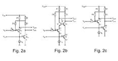
- FIG. 2a depicts as a simplified circuit diagram a principle of the amplifier 106, in accordance with an embodiment.
- the amplifier 106 may be, for example, a low noise amplifier with balun functionality.
- the amplifier 106 of Figure 2a may be based on one common-gate stage (M CG ) and one common-source stage (M CS ) which are connected in parallel. Both the common-gate stage M CG and the common-source stage M CS may operate on the single-ended input signal V in .
- the common-source stage M CS inverts the input signal V in and by designing substantially equal gains for both the common-gate stage M CG and common-source stage M CS an amplified differential version of the input signal may be obtained at a differential output V out+ , V out-
- the common-gate stage M CG may comprise a first transconductance element such as a transistor, and the common-source stage M CS may comprise a second transconductance element such as a transistor. This will be illustrated later in this specification in connection with description of Figures 2c-2f .
- the first transconductance element and the second transconductance element may be, for example, field effect transistors (FET), such as metal-oxide silicon FETs (MOSFET) or junction gate field effect transistors (JFET), or other appropriate kinds of transistors, such as bipolar transistors.
- FET field effect transistors
- MOSFET metal-oxide silicon FETs
- JFET junction gate field effect transistors
- the common-gate configuration may also be called as common-base configuration and the common-source configuration may also be called as common-emitter configuration.
- a base of a bipolar transistor may be regarded as the gate of the field effect transistor
- an emitter of a bipolar transistor may be regarded as the source of the field effect transistor
- a collector of a bipolar transistor may be regarded as the drain of the field effect transistor.
- a transconductance of the common-gate stage M CG may be raised by creating and feeding the inverted version of the single-ended input signal to the common-gate stage M CG . This may modify the matching condition of the common-gate stage M CG compared to solutions without the feedback.
- the inverted version of the input signal may not be directly available in the single-ended construction.
- a replica of the inverted input signal may then be obtained by using the inverted output voltage V out- and feeding it via a voltage divider to the gate of the common-gate stage M CG attenuated by an attenuation factor, which is the inverse of the stage voltage gain.
- the circuitry thus mimics the operation of cross-coupling on common-gate stages without requiring a differential input.
- the voltage division may be obtained, for example, by using in-series connected impedances Z2, Z3 and coupling a mutual connection of the impedances Z2, Z3 to the gate of the common-gate stage M CG via a feedback impedance Zfb.
- Feeding the inverted version of the single-ended input signal to the common-gate stage M CG may provide a higher maximum gain of the amplifier, lower noise figure (NF) and/or greater output headroom for improved linearity and design freedom.
- NF noise figure
- Figure 2b shows a modified structure of the amplifier of Figure 2a .
- cascode stages are used for both the common-gate stage M CG and the common-source stage M CS .
- the output of the common-gate stage M CG is coupled to a first buffer element B1
- the output of the common-source stage M CG is coupled to a second buffer element B2.
- the output of the first buffer element B1 may then be used as the positive voltage output V out+
- the output of the second buffer element B2 may then be used as the inverted voltage output V out- .
- the cascode stages may improve the isolation between the amplifier input and the amplifier output, and they may also extend the operating frequency range of the input by reducing the Miller effect on the common-source stage M CS .
- Figures 2c-2f illustrate some example implementations of the amplifier 106, based on the structure of Figure 2a .
- FIG 2c a simplified diagram of the amplifier structure of Figure 2a using resistive impedances is illustrated, in accordance with an embodiment.
- the common-gate stage M CG is formed by a first transistor T1 and the common-source M CS stage is formed by a second transistor T2.
- the first transistor T1 is provided with a bias voltage V B via a bias resistor R B to set a correct operation point for the first transistor.
- a source S1 of the first transistor T1 is coupled to a gate G2 of the second transistor T2.
- the gate G2 of the second transistor T2 is also used as a single-ended input for the signal to be amplified V in .
- a constant current source I B is coupled between the source S1 of the first transistor T1 and ground for biasing the first transistor T 1.
- a drain D1 of the first transistor T1 forms a positive output V out+ of the amplifier 106 and a drain D2 of the second transistor T2 forms a negative output V out- of the amplifier 106.
- An operating voltage V DD is supplied to the drain D1 of the first transistor T1 via a first resistance R1
- an operating voltage V DD is supplied to the drain D2 of the second transistor T2 via a second resistance R2 and a third resistance R3, which are connected in series.
- the second resistance R2 and the third resistance R3 form the voltage divider, wherein an attenuated, inverted output voltage V out- is provided via the feedback resistance Rfb to the gate of the first transistor T1.
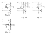
- Figure 2d illustrates a simplified diagram of the amplifier structure of Figure 2a using resistive impedances and a capacitance Cfb at the feedback loop, in accordance with an embodiment.
- the capacitance Cfb may help to not complicate the bias conditions at the gate of the common-gate stage M CG .
- the other elements of the amplifier of Figure 2d may be similar to the example of Figure 2c .
- FIG 2e a simplified diagram of the amplifier structure of Figure 2a using frequency tuned load impedances is illustrated, in accordance with an embodiment.
- the feedback loop only comprises a capacitance Cfb connected between the gate of the first transistor T1 and the mutual connection point of the second resistance R2 and the third resistance R3.
- the operating voltage V DD is supplied to the drain D1 of the first transistor T1 via a first resonance circuit formed of the first resistance R1, the first capacitance C1 and a first inductor L1, each connected in parallel.
- a second resonance circuit is formed between the inverted output V out- and the supply voltage V DD by using a second inductor L23 and a second capacitance C23.
- Forming the feedback loop by the capacitance Cfb instead of the resistance Rfb may provide the benefit of separating the DC bias conditions of the common-gate stage M CG from those at the drain of the common-source stage M CS , and of not adding substantially any noise.
- the differential outputs can be tuned to a given operating frequency by using the LC resonators L 1 /C 1 and L 23 /C 23 .
- the first inductance L 1 and the second inductance L 23 may be realized together as one center-tapped inductor, where the center tap is connected to the voltage supply line V DD .
- the first capacitance C1 and the second capacitance C23 can be implemented separately as in Figure 2e , or as one capacitor connected between the output nodes V out+ and V out .
- the use of these LC tuning circuits may make the amplifier 106 inherently narrowband in nature.
- their placement in parallel with the resistances R 1 /R 2 /R 3 may be taken into account when selecting component values so that the loads seen by common-gate stage M CG and the common-source stage M CS are substantially equal.
- FIG 2f a simplified diagram of the amplifier structure of Figure 2a using both capacitive and resistive impedances is illustrated, in accordance with an embodiment.
- the feedback loop comprises the feedback capacitance Cfb without the feedback resistance Rfb of the embodiment of Figure 2c .
- g m,CG is the transconductance of the common-gate state, which corresponds to the transconductance of the first transistor T1.
- the feedback to the gate of the common-gate stage M CG is handled capacitively through the feedback capacitance C fb , thus substantially avoiding any additional noise.
- the transconductance of the common-source stage in other words, the transconductance of the second transistor T2 in the embodiment of Figure 2f , may be selected so that it is twice a multiple of the scaling factor m of the transconductance of the common-gate stage M CG .
- Figure 2g depicts as a simplified circuit diagram the principle of the amplifier 106 of Figure 2a , but using p-type transistors instead of n-type transistors, in accordance with an embodiment.
- Transconductance-boosting the common-gate stage M CG may halve the required DC bias current of the stage and thus may halve the voltage headroom loss for the load resistance R CG of the common-gate stage.
- the increased available headroom may enable further versatility through a choice between two alternative design strategies.
- the halved headroom loss for a constant R CG can be used to provide improved linearity without affecting the noise figure or the voltage gain (A v ).
- the amplifier may allow to double R CG to obtain lower voltage swing headroom, but to simultaneously obtain much lower noise figure and doubled voltage gain.
- the doubled voltage gain may also substantially reduce the noise contribution of subsequent receiver stages, thus leading to further reduced noise figure of the receiver.
- the load resistances R1, R2, R3 may be selected as follows, in accordance with an embodiment.
- the common-gate stage M CG and the common-source stage M CS may both retain substantially equal voltage gains through this scaling and thus may retain the balun property of the amplifier 106, but the noise of the dominating the common-source stage M CS may be reduced.
- R CS R CG / m
- a very small size may be a problem in terms of fabrication process variations. This might lead to degraded common-gate stage M CG /common-source stage M CS gain balancing and thus degraded balun operation.
- the potentially doubled scaling factor m may further reduce the noise figure of the amplifier 106.
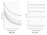
- Figure 3a illustrates the headroom loss in volts as a function of the common-gate stage load resistance R CG (line 302) and the headroom loss in volts as a function of the common-gate stage load resistance R CG (line 304) when no feedback has been used, in accordance with an embodiment.
- the amplifier structure presented above may provide greater design freedom and performance versatility than amplifier structures which do not utilize the feedback.
- the increased voltage headroom of the common-gate stage M CG may improve linearity, without a penalty on A v /NF.
- the common-gate stage M CG load resistor size may be doubled to obtain the same headroom as in amplifier structures which do not utilize the feedback, but with substantially reduced noise figure and increased voltage gain A v that in turn may decrease the noise contribution of subsequent receiver stages.
- the amplifier structure may also enable greater common-gate stage M CG / common-gate stage M CS scaling, thus decreasing the noise figure NF of the amplifier and further stages of the receiver.
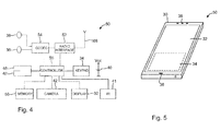
- Figure 4 shows a schematic block diagram of an exemplary apparatus or electronic device 50 depicted in Figure 5 , which may incorporate a transmitter according to an embodiment of the invention.
- the electronic device 50 may for example be a mobile terminal or user equipment of a wireless communication system. However, it would be appreciated that embodiments of the invention may be implemented within any electronic device or apparatus which may require transmission of radio frequency signals.
- the apparatus 50 may comprise a housing 30 for incorporating and protecting the device.
- the apparatus 50 further may comprise a display 32 in the form of a liquid crystal display.
- the display may be any suitable display technology suitable to display an image or video.
- the apparatus 50 may further comprise a keypad 34.
- any suitable data or user interface mechanism may be employed.
- the user interface may be implemented as a virtual keyboard or data entry system as part of a touch-sensitive display.
- the apparatus may comprise a microphone 36 or any suitable audio input which may be a digital or analogue signal input.
- the apparatus 50 may further comprise an audio output device which in embodiments of the invention may be any one of: an earpiece 38, speaker, or an analogue audio or digital audio output connection.
- the apparatus 50 may also comprise a battery 40 (or in other embodiments of the invention the device may be powered by any suitable mobile energy device such as solar cell, fuel cell or clockwork generator).
- the term battery discussed in connection with the embodiments may also be one of these mobile energy devices.
- the apparatus 50 may comprise a combination of different kinds of energy devices, for example a rechargeable battery and a solar cell.
- the apparatus may further comprise an infrared port 41 for short range line of sight communication to other devices.
- the apparatus 50 may further comprise any suitable short range communication solution such as for example a Bluetooth wireless connection or a USB/firewire wired connection.
- the apparatus 50 may comprise a controller 56 or processor for controlling the apparatus 50.
- the controller 56 may be connected to memory 58 which in embodiments of the invention may store both data and/or may also store instructions for implementation on the controller 56.
- the controller 56 may further be connected to codec circuitry 54 suitable for carrying out coding and decoding of audio and/or video data or assisting in coding and decoding carried out by the controller 56.
- the apparatus 50 may further comprise a card reader 48 and a smart card 46, for example a universal integrated circuit card (UICC) reader and a universal integrated circuit card for providing user information and being suitable for providing authentication information for authentication and authorization of the user at a network.
- a card reader 48 and a smart card 46 for example a universal integrated circuit card (UICC) reader and a universal integrated circuit card for providing user information and being suitable for providing authentication information for authentication and authorization of the user at a network.
- a card reader 48 and a smart card 46 for example a universal integrated circuit card (UICC) reader and a universal integrated circuit card for providing user information and being suitable for providing authentication information for authentication and authorization of the user at a network.
- UICC universal integrated circuit card
- the apparatus 50 may comprise radio interface circuitry 52 connected to the controller and suitable for generating wireless communication signals for example for communication with a cellular communications network, a wireless communications system or a wireless local area network.
- the apparatus 50 may further comprise an antenna 108 connected to the radio interface circuitry 52 for transmitting radio frequency signals generated at the radio interface circuitry 52 to other apparatus(es) and for receiving radio frequency signals from other apparatus(es).
- the apparatus 50 comprises a camera 42 capable of recording or detecting imaging.
- the system 10 comprises multiple communication devices which can communicate through one or more networks.
- the system 10 may comprise any combination of wired and/or wireless networks including, but not limited to a wireless cellular telephone network (such as a global systems for mobile communications (GSM), universal mobile telecommunications system (UMTS), long term evolution (LTE) based network, code division multiple access (CDMA) network etc.), a wireless local area network (WLAN) such as defined by any of the IEEE 802.x standards, a Bluetooth personal area network, an Ethernet local area network, a token ring local area network, a wide area network, and the Internet.
- GSM global systems for mobile communications
- UMTS universal mobile telecommunications system
- LTE long term evolution
- CDMA code division multiple access
- the system shown in Figure 6 shows a mobile telephone network 11 and a representation of the internet 28.
- Connectivity to the internet 28 may include, but is not limited to, long range wireless connections, short range wireless connections, and various wired connections including, but not limited to, telephone lines, cable lines, power lines, and similar communication pathways.
- the example communication devices shown in the system 10 may include, but are not limited to, an electronic device or apparatus 50, a combination of a personal digital assistant (PDA) and a mobile telephone 14, a PDA 16, an integrated messaging device (IMD) 18, a desktop computer 20, a notebook computer 22, a tablet computer.
- PDA personal digital assistant
- IMD integrated messaging device
- the apparatus 50 may be stationary or mobile when carried by an individual who is moving.
- the apparatus 50 may also be located in a mode of transport including, but not limited to, a car, a truck, a taxi, a bus, a train, a boat, an airplane, a bicycle, a motorcycle or any similar suitable mode of transport.
- Some or further apparatus may send and receive calls and messages and communicate with service providers through a wireless connection 25 to a base station 24.
- the base station 24 may be connected to a network server 26 that allows communication between the mobile telephone network 11 and the internet 28.
- the system may include additional communication devices and communication devices of various types.
- the communication devices may communicate using various transmission technologies including, but not limited to, code division multiple access (CDMA), global systems for mobile communications (GSM), universal mobile telecommunications system (UMTS), time divisional multiple access (TDMA), frequency division multiple access (FDMA), transmission control protocol-internet protocol (TCP-IP), short messaging service (SMS), multimedia messaging service (MMS), email, instant messaging service (IMS), Bluetooth, IEEE 802.11, Long Term Evolution wireless communication technique (LTE) and any similar wireless communication technology.
- CDMA code division multiple access
- GSM global systems for mobile communications
- UMTS universal mobile telecommunications system
- TDMA time divisional multiple access
- FDMA frequency division multiple access
- TCP-IP transmission control protocol-internet protocol
- SMS short messaging service
- MMS multimedia messaging service
- email instant messaging service
- IMS instant messaging service
- Bluetooth IEEE 802.11, Long Term Evolution wireless communication technique (LTE) and any similar wireless communication technology.
- LTE Long Term Evolution wireless communication technique
- embodiments of the invention operating within a wireless communication device
- the invention as described above may be implemented as a part of any apparatus comprising a circuitry in which radio frequency signals are transmitted and received.
- embodiments of the invention may be implemented in a mobile phone, in a base station, in a computer such as a desktop computer or a tablet computer comprising radio frequency communication means (e.g. wireless local area network, cellular radio, etc.).
- radio frequency communication means e.g. wireless local area network, cellular radio, etc.
- the various embodiments of the invention may be implemented in hardware or special purpose circuits or any combination thereof. While various aspects of the invention may be illustrated and described as block diagrams or using some other pictorial representation, it is well understood that these blocks, apparatus, systems, techniques or methods described herein may be implemented in, as non-limiting examples, hardware, software, firmware, special purpose circuits or logic, general purpose hardware or controller or other computing devices, or some combination thereof.
- Embodiments of the inventions may be practiced in various components such as integrated circuit modules.
- the design of integrated circuits is by and large a highly automated process.
- Complex and powerful software tools are available for converting a logic level design into a semiconductor circuit design ready to be etched and formed on a semiconductor substrate.
- Programs such as those provided by Synopsys, Inc. of Mountain View, California and Cadence Design, of San Jose, California automatically route conductors and locate components on a semiconductor chip using well established rules of design as well as libraries of pre stored design modules.
- the resultant design in a standardized electronic format (e.g., Opus, GDSII, or the like) may be transmitted to a semiconductor fabrication facility or "fab" for fabrication.
- a method comprising:
- an apparatus comprising:
- the first transconducting element and the second transconducting element are field effect transistors.
- the apparatus is a part of a receiver.
- the apparatus is a part of a wireless communication device.
- an apparatus comprising:
Landscapes
- Engineering & Computer Science (AREA)
- Power Engineering (AREA)
- Microelectronics & Electronic Packaging (AREA)
- Amplifiers (AREA)
Abstract
Description
- The present invention relates to a method for amplifying signals and an apparatus for amplifying signals.
- This section is intended to provide a background or context to the invention that is recited in the claims. The description herein may include concepts that could be pursued, but are not necessarily ones that have been previously conceived or pursued. Therefore, unless otherwise indicated herein, what is described in this section is not prior art to the description and claims in this application and is not admitted to be prior art by inclusion in this section.
- In some apparatuses a low-noise amplifier (LNA) may be used to amplify signals so that noise possibly contributed by the amplifier is as weak as possible. These kinds of amplifiers may be used, for example, in radio receivers in a so called radio frequency (RF) front end. The low noise amplifier is intended to amplify possibly quite weak signals received by an antenna before the received signals are coupled to a mixer for converting the radio frequency signals to intermediate frequency (IF) signals or to baseband (BB) signals.
- Receivers implemented on semiconductor circuits such as complementary metal oxide silicon circuits (CMOS) may operate with differential signaling. While differential signaling may consume more power and circuit area compared to single-ended solutions, the differential signaling may enable doubled signal swing and better noise immunity. However, differential low noise amplifiers may need two high-frequency input/output (I/O) pads on the integrated circuit instead of one. Especially multi-band/multi-mode receivers may use several parallel low noise amplifiers wherein at least some circuit area may be saved if a single-ended input could be utilized by the low noise amplifier. This may be achieved by performing single-ended to differential (i.e., unbalanced to balanced) conversion on-chip in the low noise amplifier structure.
- Various embodiments provide a method and apparatus for amplifying signals and an apparatus for amplifying signals.
- Various aspects of examples of the invention are provided in the detailed description.
- According to a first aspect, there is provided a method comprising:
- providing a signal to an input of a first transconducting element;
- forming an amplified signal on the basis of the input signal by the first transconducting element and a second transconducting element;
- using the amplified signal to form an inverted signal; and
- providing the inverted signal to another input of the first transconducting element.
- According to a second aspect, there is provided an apparatus comprising:
- a first transconducting element comprising an input for inputting a signal;
- a second transconducting element;
- wherein the first transconducting element and the second transconducting element are adapted for forming an amplified signal on the basis of the input signal;
- an element for forming an inverted signal from the amplified signal; and
- a feedback element for providing the inverted signal to another input of the first transconducting element.
- According to a third aspect, there is provided an apparatus comprising:
- means for providing a signal to an input of a first transconducting element;
- means for forming an amplified signal on the basis of the input signal by the first transconducting element and a second transconducting element;
- means for using the amplified signal to form an inverted signal; and
- means for providing the inverted signal to another input of the first transconducting element.
- For a more complete understanding of example embodiments of the present invention, reference is now made to the following descriptions taken in connection with the accompanying drawings in which:
-
Figure 1 shows a simplified block diagram of a device according to an example embodiment; -
Figure 2a illustrates as a simplified circuit diagram the structure of an amplifier, in accordance with an embodiment; -
Figure 2b illustrates as a simplified diagram an example of the structure of an amplifier utilizing cascode construction, in accordance with an embodiment; -
Figure 2c illustrates as a simplified diagram an example of the structure of an amplifier using resistive impedances, in accordance with an embodiment; -
Figure 2d illustrates as a simplified diagram an example of the structure of an amplifier using both capacitive and resistive impedances, in accordance with an embodiment; -
Figure 2e illustrates as a simplified diagram an example of the structure of an amplifier using frequency tuned load impedances, in accordance with an embodiment; -
Figure 2f illustrates as a simplified diagram an example of the structure of an amplifier using a capacitance at a feedback loop, in accordance with an embodiment; -
Figure 2g illustrates as a simplified circuit diagram the structure of an amplifier ofFigure 2a using p-type transistors, in accordance with an embodiment; -
Figure 3a illustrates a headroom loss in volts as a function of a common-gate stage load resistance and a headroom loss in volts as a function of the common-gate stage load resistance RCG when no feedback has been used, in accordance with an embodiment; -
Figures 3b and 3c illustrate some simulation results of a noise figure and gain of the amplifier for different values of load resistance and attenuation factor, in accordance with another embodiment; -
Figure 4 shows a block diagram of an apparatus according to an example embodiment; -
Figure 5 shows an apparatus according to an example embodiment; -
Figure 6 shows an example of an arrangement for wireless communication comprising a plurality of apparatuses, networks and network elements. - The following embodiments are exemplary. Although the specification may refer to "an", "one", or "some" embodiment(s) in several locations, this does not necessarily mean that each such reference is to the same embodiment(s), or that the feature only applies to a single embodiment. Single features of different embodiments may also be combined to provide other embodiments.
-
Figure 1 depicts an example of a part of adevice 100, which may be, for example, a mobile device such as a mobile phone, but may also be another device comprising anamplifier 106. Thedevice 100 may be constructed to include thefrequency synthesizer 101 for generating one or more oscillator signals. The device may comprise one ormore data processors 102 for controlling the operations of the device, in accordance with an embodiment. Thedata processor 102 operates in accordance with program instructions stored in at least one storage medium, such as at least onememory 103. Thedata processor 102 may control thefrequency synthesizer 101 for setting the output frequency/frequencies of thefrequency synthesizer 101. These output frequencies form one or more local oscillator signals that may be applied simultaneously to anRF receiver circuitry 104. TheRF receiver circuitry 104 may include one or multiple instances offilters 105,amplifiers 106 andmixers 107. TheRF receiver circuitry 104 may be configured to be connected with at least one, and possiblyseveral antennas 108, and may operate to simultaneously receive and down-convert multiple reception channels in multiple frequency bands. TheRF receiver circuitry 104 may be implemented e.g. as a single direct conversion receiver, as a plurality of direct conversion receivers, as a single superheterodyne-type receiver or as a plurality of superheterodyne-type receivers. In either case the down-converted signals from multiple reception channels are provided to at least onebaseband circuitry block 109 to demodulate and decode received signaling and other data. - The device of
Figure 1 also comprises anRF transmitter 110 for transmitting radio frequency signals. Thetransmitter 110 may comprise one ormore mixers 111 adapted to receive signals to be transmitted and a local oscillator signal LO2. The mixing result may be provided to aband pass filter 112 to filter out mixing results which are out of the transmission band, and apower amplifier 113 to amplify the RF signals before passing them to one ormore antennas 108. The one ormore antennas 108 may be the same one or more antennas than theRF receiver circuitry 104 uses or different antenna(s). - The
RF receiver circuitry 104, theRF transmitter 110 and/or thebaseband circuitry 109 may be embodied as an integrated circuit. In some embodiments theRF receiver circuitry 104, theRF transmitter 110 and thebaseband circuitry 109 or parts of them may be embodied in the same integrated circuit, and in some other embodiments they may be embodied in different integrated circuits. In some embodiments all of the circuitry shown inFigure 1 , including thedata processor 102 and possibly also thememory 103, may be embodied in one integrated circuit module or package. - In some embodiments all or some of the functionality of the
frequency synthesizer 101 may be embodied by thedata processor 102 or by another data processor, such as a high speed digital signal processor operating under control of a stored program. -
Figure 2a depicts as a simplified circuit diagram a principle of theamplifier 106, in accordance with an embodiment. Theamplifier 106 may be, for example, a low noise amplifier with balun functionality. Theamplifier 106 ofFigure 2a may be based on one common-gate stage (MCG) and one common-source stage (MCS) which are connected in parallel. Both the common-gate stage MCG and the common-source stage MCS may operate on the single-ended input signal Vin. The common-source stage MCS inverts the input signal Vin and by designing substantially equal gains for both the common-gate stage MCG and common-source stage MCS an amplified differential version of the input signal may be obtained at a differential output Vout+, Vout- - The common-gate stage MCG may comprise a first transconductance element such as a transistor, and the common-source stage MCS may comprise a second transconductance element such as a transistor. This will be illustrated later in this specification in connection with description of
Figures 2c-2f . - The first transconductance element and the second transconductance element may be, for example, field effect transistors (FET), such as metal-oxide silicon FETs (MOSFET) or junction gate field effect transistors (JFET), or other appropriate kinds of transistors, such as bipolar transistors.
- If bipolar transistors are uses as the transconductance elements, the common-gate configuration may also be called as common-base configuration and the common-source configuration may also be called as common-emitter configuration. In the circuitries, a base of a bipolar transistor may be regarded as the gate of the field effect transistor, an emitter of a bipolar transistor may be regarded as the source of the field effect transistor, and a collector of a bipolar transistor may be regarded as the drain of the field effect transistor.
- A transconductance of the common-gate stage MCG may be raised by creating and feeding the inverted version of the single-ended input signal to the common-gate stage MCG. This may modify the matching condition of the common-gate stage MCG compared to solutions without the feedback. The inverted version of the input signal may not be directly available in the single-ended construction. A replica of the inverted input signal may then be obtained by using the inverted output voltage Vout- and feeding it via a voltage divider to the gate of the common-gate stage MCG attenuated by an attenuation factor, which is the inverse of the stage voltage gain. In effect, the circuitry thus mimics the operation of cross-coupling on common-gate stages without requiring a differential input.
- The voltage division may be obtained, for example, by using in-series connected impedances Z2, Z3 and coupling a mutual connection of the impedances Z2, Z3 to the gate of the common-gate stage MCG via a feedback impedance Zfb. The division ratio (attenuation factor) may be determined by the following equation:

- Feeding the inverted version of the single-ended input signal to the common-gate stage MCG may provide a higher maximum gain of the amplifier, lower noise figure (NF) and/or greater output headroom for improved linearity and design freedom.
- In accordance with an embodiment, the feedback may affect the input matching condition of the common-gate stage MCG such that it becomes gm,CG = 10 mS for a 50-Ω system instead of gm,CG = 20 mS for a 50-Ω system.
-
Figure 2b shows a modified structure of the amplifier ofFigure 2a . In this structure cascode stages are used for both the common-gate stage MCG and the common-source stage MCS. In other words, the output of the common-gate stage MCG is coupled to a first buffer element B1, and the output of the common-source stage MCG is coupled to a second buffer element B2. The output of the first buffer element B1 may then be used as the positive voltage output Vout+, and the output of the second buffer element B2 may then be used as the inverted voltage output Vout-. The cascode stages may improve the isolation between the amplifier input and the amplifier output, and they may also extend the operating frequency range of the input by reducing the Miller effect on the common-source stage MCS. -
Figures 2c-2f illustrate some example implementations of theamplifier 106, based on the structure ofFigure 2a . - In
Figure 2c a simplified diagram of the amplifier structure ofFigure 2a using resistive impedances is illustrated, in accordance with an embodiment. The common-gate stage MCG is formed by a first transistor T1 and the common-source MCS stage is formed by a second transistor T2. The first transistor T1 is provided with a bias voltage VB via a bias resistor RB to set a correct operation point for the first transistor. A source S1 of the first transistor T1 is coupled to a gate G2 of the second transistor T2. The gate G2 of the second transistor T2 is also used as a single-ended input for the signal to be amplified Vin. A constant current source IB is coupled between the source S1 of the first transistor T1 and ground for biasing thefirst transistor T 1. A drain D1 of the first transistor T1 forms a positive output Vout+ of theamplifier 106 and a drain D2 of the second transistor T2 forms a negative output Vout- of theamplifier 106. An operating voltage VDD is supplied to the drain D1 of the first transistor T1 via a first resistance R1, and an operating voltage VDD is supplied to the drain D2 of the second transistor T2 via a second resistance R2 and a third resistance R3, which are connected in series. The second resistance R2 and the third resistance R3 form the voltage divider, wherein an attenuated, inverted output voltage Vout- is provided via the feedback resistance Rfb to the gate of the first transistor T1. -
Figure 2d illustrates a simplified diagram of the amplifier structure ofFigure 2a using resistive impedances and a capacitance Cfb at the feedback loop, in accordance with an embodiment. The capacitance Cfb may help to not complicate the bias conditions at the gate of the common-gate stage MCG. The other elements of the amplifier ofFigure 2d may be similar to the example ofFigure 2c . - In
Figure 2e a simplified diagram of the amplifier structure ofFigure 2a using frequency tuned load impedances is illustrated, in accordance with an embodiment. The feedback loop only comprises a capacitance Cfb connected between the gate of the first transistor T1 and the mutual connection point of the second resistance R2 and the third resistance R3. The operating voltage VDD is supplied to the drain D1 of the first transistor T1 via a first resonance circuit formed of the first resistance R1, the first capacitance C1 and a first inductor L1, each connected in parallel. A second resonance circuit is formed between the inverted output Vout- and the supply voltage VDD by using a second inductor L23 and a second capacitance C23. - Forming the feedback loop by the capacitance Cfb instead of the resistance Rfb may provide the benefit of separating the DC bias conditions of the common-gate stage MCG from those at the drain of the common-source stage MCS, and of not adding substantially any noise.
- In the construction of
Figure 2e the differential outputs can be tuned to a given operating frequency by using the LC resonators L1/C1 and L23/C23. The first inductance L1 and the second inductance L23 may be realized together as one center-tapped inductor, where the center tap is connected to the voltage supply line VDD. The first capacitance C1 and the second capacitance C23 can be implemented separately as inFigure 2e , or as one capacitor connected between the output nodes Vout+ and Vout. The use of these LC tuning circuits may make theamplifier 106 inherently narrowband in nature. Moreover, their placement in parallel with the resistances R1/R2/R3 may be taken into account when selecting component values so that the loads seen by common-gate stage MCG and the common-source stage MCS are substantially equal. - In
Figure 2f a simplified diagram of the amplifier structure ofFigure 2a using both capacitive and resistive impedances is illustrated, in accordance with an embodiment. The feedback loop comprises the feedback capacitance Cfb without the feedback resistance Rfb of the embodiment ofFigure 2c . - The lack of LC resonators may provide wideband operation and may avoid possible resonator-related difficulties for balancing the load impedances. Instead, this construction only uses resistances, where the common-source branch resistive-divider load R2/R3 may be sized such that its gain (attenuation) is substantially the inverse of the voltage gain of the branches, i.e., β = 1/gm,CGRCG. Using the markings of
Figure 2f , in which the resistance R1 corresponds with the common-gate branch resistance RCG, the gain may be expressed as β = 1/gm,CGR1. gm,CG is the transconductance of the common-gate state, which corresponds to the transconductance of the first transistor T1. The feedback to the gate of the common-gate stage MCG is handled capacitively through the feedback capacitance Cfb, thus substantially avoiding any additional noise. - The transconductance of the common-source stage, in other words, the transconductance of the second transistor T2 in the embodiment of
Figure 2f , may be selected so that it is twice a multiple of the scaling factor m of the transconductance of the common-gate stage MCG. Hence, the common-source stage MCS load resistor RCS (=R2+R3) may be designed as RCG/m and the transconductance of the common-source stage would be gm,CS = 2*m*gm,CG. -
Figure 2g depicts as a simplified circuit diagram the principle of theamplifier 106 ofFigure 2a , but using p-type transistors instead of n-type transistors, in accordance with an embodiment. - Transconductance-boosting the common-gate stage MCG may halve the required DC bias current of the stage and thus may halve the voltage headroom loss for the load resistance RCG of the common-gate stage. The increased available headroom may enable further versatility through a choice between two alternative design strategies. On the one hand, the halved headroom loss for a constant RCG can be used to provide improved linearity without affecting the noise figure or the voltage gain (Av). Furthermore, the amplifier may allow to double RCG to obtain lower voltage swing headroom, but to simultaneously obtain much lower noise figure and doubled voltage gain. The doubled voltage gain may also substantially reduce the noise contribution of subsequent receiver stages, thus leading to further reduced noise figure of the receiver.
- Using the above mentioned notations and equations, the load resistances R1, R2, R3 may be selected as follows, in accordance with an embodiment. R1 = RCG, R2 = βRCG/m, and R3 = (1-β)RCG/m. Thus, the common-gate stage MCG and the common-source stage MCS may both retain substantially equal voltage gains through this scaling and thus may retain the balun property of the
amplifier 106, but the noise of the dominating the common-source stage MCS may be reduced. - Specifically, the potentially doubled value of the common-gate stage MCG load resistance RCG in the amplifier may allow to use up to a doubled scaling factor m before making the common-source stage MCS load resistor (RCS = RCG/m) unreasonably small. A very small size may be a problem in terms of fabrication process variations. This might lead to degraded common-gate stage MCG/common-source stage MCS gain balancing and thus degraded balun operation. The potentially doubled scaling factor m may further reduce the noise figure of the
amplifier 106. -
Figure 3a illustrates the headroom loss in volts as a function of the common-gate stage load resistance RCG (line 302) and the headroom loss in volts as a function of the common-gate stage load resistance RCG (line 304) when no feedback has been used, in accordance with an embodiment.Figures 3b and 3c illustrate some simulation results of the noise figure and gain of theamplifier 106 for different values of RCG and m, in accordance with an embodiment. In the simulations it was assumed that the transistor noise constant is γ = 2/3. For example, if RCG = 200 and m = 2, the noise figure NF is about 2.4 dB (curve 306) and the gain is about 15 dB (curve 316). The other simulated results were as follows: thecurve 304 illustrates the noise figure and thecurve 314 illustrates the gain, when RCG = 100; thecurve 308 illustrates the noise figure and thecurve 318 illustrates the gain, when RCG = 300; thecurve 310 illustrates the noise figure and thecurve 320 illustrates the gain, when RCG = 400; and thecurve 312 illustrates the noise figure and thecurve 322 illustrates the gain, when RCG = 500. - In accordance with an embodiment, the amplifier may be designed so that RCG = 400 and m = 2, which leads to the noise figure of 1.9 dB and gain = 21 dB. In accordance with another embodiment, the amplifier may be designed so that RCG = 400 and m = 3, wherein this may lead to a further improved noise figure NF = 1.5 dB.
- The amplifier structure presented above may provide greater design freedom and performance versatility than amplifier structures which do not utilize the feedback. The increased voltage headroom of the common-gate stage MCG may improve linearity, without a penalty on Av/NF. Further, the common-gate stage MCG load resistor size may be doubled to obtain the same headroom as in amplifier structures which do not utilize the feedback, but with substantially reduced noise figure and increased voltage gain Av that in turn may decrease the noise contribution of subsequent receiver stages. The amplifier structure may also enable greater common-gate stage MCG / common-gate stage MCS scaling, thus decreasing the noise figure NF of the amplifier and further stages of the receiver.
- The following describes in further detail suitable apparatus and possible mechanisms for implementing the embodiments of the invention. In this regard reference is first made to
Figure 4 which shows a schematic block diagram of an exemplary apparatus orelectronic device 50 depicted inFigure 5 , which may incorporate a transmitter according to an embodiment of the invention. - The
electronic device 50 may for example be a mobile terminal or user equipment of a wireless communication system. However, it would be appreciated that embodiments of the invention may be implemented within any electronic device or apparatus which may require transmission of radio frequency signals. - The
apparatus 50 may comprise ahousing 30 for incorporating and protecting the device. Theapparatus 50 further may comprise adisplay 32 in the form of a liquid crystal display. In other embodiments of the invention the display may be any suitable display technology suitable to display an image or video. Theapparatus 50 may further comprise akeypad 34. In other embodiments of the invention any suitable data or user interface mechanism may be employed. For example the user interface may be implemented as a virtual keyboard or data entry system as part of a touch-sensitive display. The apparatus may comprise amicrophone 36 or any suitable audio input which may be a digital or analogue signal input. Theapparatus 50 may further comprise an audio output device which in embodiments of the invention may be any one of: anearpiece 38, speaker, or an analogue audio or digital audio output connection. Theapparatus 50 may also comprise a battery 40 (or in other embodiments of the invention the device may be powered by any suitable mobile energy device such as solar cell, fuel cell or clockwork generator). The term battery discussed in connection with the embodiments may also be one of these mobile energy devices. Further, theapparatus 50 may comprise a combination of different kinds of energy devices, for example a rechargeable battery and a solar cell. The apparatus may further comprise aninfrared port 41 for short range line of sight communication to other devices. In other embodiments theapparatus 50 may further comprise any suitable short range communication solution such as for example a Bluetooth wireless connection or a USB/firewire wired connection. - The
apparatus 50 may comprise acontroller 56 or processor for controlling theapparatus 50. Thecontroller 56 may be connected tomemory 58 which in embodiments of the invention may store both data and/or may also store instructions for implementation on thecontroller 56. Thecontroller 56 may further be connected tocodec circuitry 54 suitable for carrying out coding and decoding of audio and/or video data or assisting in coding and decoding carried out by thecontroller 56. - The
apparatus 50 may further comprise acard reader 48 and asmart card 46, for example a universal integrated circuit card (UICC) reader and a universal integrated circuit card for providing user information and being suitable for providing authentication information for authentication and authorization of the user at a network. - The
apparatus 50 may compriseradio interface circuitry 52 connected to the controller and suitable for generating wireless communication signals for example for communication with a cellular communications network, a wireless communications system or a wireless local area network. Theapparatus 50 may further comprise anantenna 108 connected to theradio interface circuitry 52 for transmitting radio frequency signals generated at theradio interface circuitry 52 to other apparatus(es) and for receiving radio frequency signals from other apparatus(es). - In some embodiments of the invention, the
apparatus 50 comprises acamera 42 capable of recording or detecting imaging. - With respect to
Figure 6 , an example of a system within which embodiments of the present invention can be utilized is shown. Thesystem 10 comprises multiple communication devices which can communicate through one or more networks. Thesystem 10 may comprise any combination of wired and/or wireless networks including, but not limited to a wireless cellular telephone network (such as a global systems for mobile communications (GSM), universal mobile telecommunications system (UMTS), long term evolution (LTE) based network, code division multiple access (CDMA) network etc.), a wireless local area network (WLAN) such as defined by any of the IEEE 802.x standards, a Bluetooth personal area network, an Ethernet local area network, a token ring local area network, a wide area network, and the Internet. - For example, the system shown in
Figure 6 shows amobile telephone network 11 and a representation of theinternet 28. Connectivity to theinternet 28 may include, but is not limited to, long range wireless connections, short range wireless connections, and various wired connections including, but not limited to, telephone lines, cable lines, power lines, and similar communication pathways. - The example communication devices shown in the
system 10 may include, but are not limited to, an electronic device orapparatus 50, a combination of a personal digital assistant (PDA) and amobile telephone 14, aPDA 16, an integrated messaging device (IMD) 18, adesktop computer 20, anotebook computer 22, a tablet computer. Theapparatus 50 may be stationary or mobile when carried by an individual who is moving. Theapparatus 50 may also be located in a mode of transport including, but not limited to, a car, a truck, a taxi, a bus, a train, a boat, an airplane, a bicycle, a motorcycle or any similar suitable mode of transport. - Some or further apparatus may send and receive calls and messages and communicate with service providers through a
wireless connection 25 to abase station 24. Thebase station 24 may be connected to anetwork server 26 that allows communication between themobile telephone network 11 and theinternet 28. The system may include additional communication devices and communication devices of various types. - The communication devices may communicate using various transmission technologies including, but not limited to, code division multiple access (CDMA), global systems for mobile communications (GSM), universal mobile telecommunications system (UMTS), time divisional multiple access (TDMA), frequency division multiple access (FDMA), transmission control protocol-internet protocol (TCP-IP), short messaging service (SMS), multimedia messaging service (MMS), email, instant messaging service (IMS), Bluetooth, IEEE 802.11, Long Term Evolution wireless communication technique (LTE) and any similar wireless communication technology. A communications device involved in implementing various embodiments of the present invention may communicate using various media including, but not limited to, radio, infrared, laser, cable connections, and any suitable connection. In the following some example implementations of apparatuses utilizing the present invention will be described in more detail.
- Although the above examples describe embodiments of the invention operating within a wireless communication device, it would be appreciated that the invention as described above may be implemented as a part of any apparatus comprising a circuitry in which radio frequency signals are transmitted and received. Thus, for example, embodiments of the invention may be implemented in a mobile phone, in a base station, in a computer such as a desktop computer or a tablet computer comprising radio frequency communication means (e.g. wireless local area network, cellular radio, etc.).
- In general, the various embodiments of the invention may be implemented in hardware or special purpose circuits or any combination thereof. While various aspects of the invention may be illustrated and described as block diagrams or using some other pictorial representation, it is well understood that these blocks, apparatus, systems, techniques or methods described herein may be implemented in, as non-limiting examples, hardware, software, firmware, special purpose circuits or logic, general purpose hardware or controller or other computing devices, or some combination thereof.
- Embodiments of the inventions may be practiced in various components such as integrated circuit modules. The design of integrated circuits is by and large a highly automated process. Complex and powerful software tools are available for converting a logic level design into a semiconductor circuit design ready to be etched and formed on a semiconductor substrate.
- Programs, such as those provided by Synopsys, Inc. of Mountain View, California and Cadence Design, of San Jose, California automatically route conductors and locate components on a semiconductor chip using well established rules of design as well as libraries of pre stored design modules. Once the design for a semiconductor circuit has been completed, the resultant design, in a standardized electronic format (e.g., Opus, GDSII, or the like) may be transmitted to a semiconductor fabrication facility or "fab" for fabrication.
- The foregoing description has provided by way of exemplary and non-limiting examples a full and informative description of the exemplary embodiment of this invention. However, various modifications and adaptations may become apparent to those skilled in the relevant arts in view of the foregoing description, when read in conjunction with the accompanying drawings and the appended claims. However, all such and similar modifications of the teachings of this invention will still fall within the scope of this invention.
- In the following some examples will be provided.
- According to a first example, there is provided a method comprising:
- providing a signal to an input of a first transconducting element;
- forming an amplified signal on the basis of the input signal by the first transconducting element and a second transconducting element;
- using the amplified signal to form an inverted signal; and
- providing the inverted signal to another input of the first transconducting element.
- In some embodiments the method comprises:
- generating the amplified signal as a differential output signal comprising a positive output signal and a negative output signal.
- In some embodiments the method comprises:
- using the negative output signal to form the inverted signal.
- In some embodiments the method comprises:
- feeding a signal amplified by the first transconducting element to a first load impedance for forming the positive output signal; and
- feeding a signal amplified by the second transconducting element to a second load impedance for forming the negative output signal.
- In some embodiments the method comprises:
- forming the inverted signal by the second load impedance.
- In some embodiments the method comprises:
- attenuating the inverted signal by the second load impedance by an attenuation factor.
- According to a second example, there is provided an apparatus comprising:
- a first transconducting element comprising an input for inputting a signal;
- a second transconducting element;
- wherein the first transconducting element and the second transconducting element are adapted for forming an amplified signal on the basis of the input signal;
- an element for forming an inverted signal from the amplified signal; and
- a feedback element for providing the inverted signal to another input of the first transconducting element.
- In some embodiments the apparatus is adapted to:
- generate the amplified signal as a differential output signal comprising a positive output signal and a negative output signal.
- In some embodiments of the apparatus:
- the first transconducting element is coupled to a first load impedance for forming the positive output signal; and
- the second transconducting element is coupled to a second load impedance for forming the negative output signal.
- In some embodiments of the apparatus:
- the second load impedance is a voltage divider to form an attenuated output signal, wherein the feedback element is coupled to the voltage divider to feed the attenuated output signal to another input of the first transconducting element.
- In some embodiments of the apparatus the voltage divider comprises:
- two impedances coupled in parallel, wherein a mutual coupling of the two impedances is coupled to the feedback element.
- In some embodiments of the apparatus:
- the first transconducting element is a part of a common-gate configuration; and
- the second transconducting element is a part of a common-source configuration.
- In some embodiments of the apparatus the load impedances comprise one or more of the following:
- resistances;
- LC resonators.
- In some embodiments of the apparatus the feedback element comprises one of the following:
- one or more resistances;
- one or more capacitances;
- one or more resistances and one or more capacitances coupled in series.
- In some embodiments of the apparatus the first transconducting element and the second transconducting element are field effect transistors.
- In some embodiments the apparatus is a part of a receiver.
- In some embodiments the apparatus is a part of a wireless communication device.
- According to a third example, there is provided an apparatus comprising:
- means for providing a signal to an input of a first transconducting element;
- means for forming an amplified signal on the basis of the input signal by the first transconducting element and a second transconducting element;
- means for using the amplified signal to form an inverted signal; and
- means for providing the inverted signal to another input of the first transconducting element.
- In some embodiments the apparatus comprises:
- means for generating the amplified signal as a differential output signal comprising a positive output signal and a negative output signal.
- In some embodiments the apparatus comprises:
- means for using the negative output signal to form the inverted signal.
- In some embodiments the apparatus comprises:
- means for feeding a signal amplified by the first transconducting element to a first load impedance for forming the positive output signal; and
- means for feeding a signal amplified by the second transconducting element to a second load impedance for forming the negative output signal.
- In some embodiments the apparatus comprises:
- means for forming the inverted signal by the second load impedance.
- In some embodiments the apparatus comprises:
- means for attenuating the inverted signal by the second load impedance by an attenuation factor.
Claims (15)
- A method comprising:providing a signal to an input of a first transconducting element;forming an amplified signal on the basis of the input signal by the first transconducting element and a second transconducting element;using the amplified signal to form an inverted signal; andproviding the inverted signal to another input of the first transconducting element.
- The method according to claim 1 comprising:generating the amplified signal as a differential output signal comprising a positive output signal and a negative output signal; andusing the negative output signal to form the inverted signal.
- The method according to claim 2 comprising:feeding a signal amplified by the first transconducting element to a first load impedance for forming the positive output signal; andfeeding a signal amplified by the second transconducting element to a second load impedance for forming the negative output signal.
- The method according to claim 3 comprising:forming the inverted signal by the second load impedance.
- The method according to claims 1 to 4 comprising:attenuating the inverted signal by the second load impedance by an attenuation factor.
- An apparatus comprising:a first transconducting element comprising an input for inputting a signal;a second transconducting element;wherein the first transconducting element and the second transconducting element are adapted for forming an amplified signal on the basis of the input signal;an element for forming an inverted signal from the amplified signal; anda feedback element for providing the inverted signal to another input of the first transconducting element.
- The apparatus according to claim 6, wherein the apparatus is adapted to:generate the amplified signal as a differential output signal comprising a positive output signal and a negative output signal.
- The apparatus according to claim 7, wherein:the first transconducting element is coupled to a first load impedance for forming the positive output signal; andthe second transconducting element is coupled to a second load impedance for forming the negative output signal.
- The apparatus according to claim 8, wherein:the second load impedance is a voltage divider to form an attenuated output signal, wherein the feedback element is coupled to the voltage divider to feed the attenuated output signal to another input of the first transconducting element.
- The apparatus according to claim 9, wherein the voltage divider comprises:two impedances coupled in parallel, wherein a mutual coupling of the two impedances is coupled to the feedback element.
- The apparatus according to claim 10, wherein the load impedances comprise one or more of the following:resistances;LC resonators.
- The apparatus according to any of the claims 6 to 11, wherein:the first transconducting element is a part of a common-gate or a common-base configuration; andthe second transconducting element is a part of a common-source or a common-emitter configuration.
- The apparatus according to any of the claims 6 to 12, wherein the feedback element comprises one of the following:one or more resistances;one or more capacitances;one or more resistances and one or more capacitances coupled in series.
- The apparatus according to any of the claims 6 to 13, wherein the first transconducting element and the second transconducting element are field effect transistors.
- The apparatus according to any of the claims 6 to 14, wherein the apparatus is a part of a receiver of a wireless communication device.
Priority Applications (2)
| Application Number | Priority Date | Filing Date | Title |
|---|---|---|---|
| EP15183224.3A EP3139498A1 (en) | 2015-09-01 | 2015-09-01 | Method and apparatus for amplifying signals |
| PCT/FI2016/050606 WO2017037346A1 (en) | 2015-09-01 | 2016-09-01 | Method and apparatus for amplifying signals |
Applications Claiming Priority (1)
| Application Number | Priority Date | Filing Date | Title |
|---|---|---|---|
| EP15183224.3A EP3139498A1 (en) | 2015-09-01 | 2015-09-01 | Method and apparatus for amplifying signals |
Publications (1)
| Publication Number | Publication Date |
|---|---|
| EP3139498A1 true EP3139498A1 (en) | 2017-03-08 |
Family
ID=54014680
Family Applications (1)
| Application Number | Title | Priority Date | Filing Date |
|---|---|---|---|
| EP15183224.3A Withdrawn EP3139498A1 (en) | 2015-09-01 | 2015-09-01 | Method and apparatus for amplifying signals |
Country Status (2)
| Country | Link |
|---|---|
| EP (1) | EP3139498A1 (en) |
| WO (1) | WO2017037346A1 (en) |
Citations (5)
| Publication number | Priority date | Publication date | Assignee | Title |
|---|---|---|---|---|
| US20030042983A1 (en) * | 2001-09-04 | 2003-03-06 | Hollenbeck Neal W. | Single ended input, differential output amplifier |
| US20040056722A1 (en) * | 2002-09-24 | 2004-03-25 | Sehat Sutardja | Ultra broadband low noise amplifier with matched reactive input impedance |
| US20100013562A1 (en) * | 2008-07-17 | 2010-01-21 | Infineon Technologies Ag | Circuit with single-ended input and differential output |
| US20120154056A1 (en) * | 2010-12-17 | 2012-06-21 | Industrial Technology Research Institute | Method and apparatus for canceling balun amplifier noise |
| US8264281B1 (en) * | 2011-06-03 | 2012-09-11 | Texas Instruments Incorporated | Low-noise amplifier with tuned input and output impedances |
Family Cites Families (1)
| Publication number | Priority date | Publication date | Assignee | Title |
|---|---|---|---|---|
| KR100856131B1 (en) * | 2006-01-18 | 2008-09-03 | 삼성전자주식회사 | Variable gain low noise amplifier circuit and wireless communication receiver having same |
-
2015
- 2015-09-01 EP EP15183224.3A patent/EP3139498A1/en not_active Withdrawn
-
2016
- 2016-09-01 WO PCT/FI2016/050606 patent/WO2017037346A1/en not_active Ceased
Patent Citations (5)
| Publication number | Priority date | Publication date | Assignee | Title |
|---|---|---|---|---|
| US20030042983A1 (en) * | 2001-09-04 | 2003-03-06 | Hollenbeck Neal W. | Single ended input, differential output amplifier |
| US20040056722A1 (en) * | 2002-09-24 | 2004-03-25 | Sehat Sutardja | Ultra broadband low noise amplifier with matched reactive input impedance |
| US20100013562A1 (en) * | 2008-07-17 | 2010-01-21 | Infineon Technologies Ag | Circuit with single-ended input and differential output |
| US20120154056A1 (en) * | 2010-12-17 | 2012-06-21 | Industrial Technology Research Institute | Method and apparatus for canceling balun amplifier noise |
| US8264281B1 (en) * | 2011-06-03 | 2012-09-11 | Texas Instruments Incorporated | Low-noise amplifier with tuned input and output impedances |
Also Published As
| Publication number | Publication date |
|---|---|
| WO2017037346A1 (en) | 2017-03-09 |
Similar Documents
| Publication | Publication Date | Title |
|---|---|---|
| CN105409116B (en) | Amplifier with Configurable Mutual Coupled Source Degeneration Inductor | |
| KR101636409B1 (en) | Amplifiers with boosted or deboosted source degeneration inductance | |
| US12081243B2 (en) | Low noise amplifiers with combined outputs | |
| CN105009448B (en) | Amplifier with multiple outputs and configurable degeneration inductor | |
| CN105009447B (en) | With inductance decline, configurable gain and the matched amplifier of input | |
| US9271239B2 (en) | Current-efficient low noise amplifier (LNA) | |
| US9246438B2 (en) | Receiver architecture for a compact and low power receiver | |
| CN101010872B (en) | Radio receiver front-end and a method for converting frequency for input signal | |
| CN111434031A (en) | Power amplifier circuit | |
| US8989688B2 (en) | Low-noise TIA-to-ADC interface with a wide-range of passive gain control | |
| CN105075114A (en) | Split amplifier with improved linearity | |
| US7671685B2 (en) | Method and system for a low power fully differential noise cancelling low noise amplifier | |
| CN110492859B (en) | Current transmitter circuit and method | |
| CN105680803A (en) | System and method for low noise amplifier module | |
| CN106233621B (en) | Differential cascode amplifier with selectively coupled gate terminals | |
| US20150163747A1 (en) | Common gate buffer having adjustable current consumption in a receiver | |
| CN107112957B (en) | Receiver front-end architecture for in-band carrier aggregation | |
| US8324966B2 (en) | Apparatus and methods for electronic amplification | |
| EP3231087B1 (en) | Low power operational transconductance amplifier | |
| EP3171513A1 (en) | Method and apparatus for amplifying signals | |
| CN106233620A (en) | The transmission gate generated for bias voltage | |
| US20250096737A1 (en) | Low-noise amplifier (lna) input impedance improvement using coupling between output inductor and degeneration inductor | |
| EP3139498A1 (en) | Method and apparatus for amplifying signals | |
| CN120814174A (en) | Kickback reduction in bootstrap switching | |
| US20180358932A1 (en) | Method and apparatus for amplifying signals |
Legal Events
| Date | Code | Title | Description |
|---|---|---|---|
| PUAI | Public reference made under article 153(3) epc to a published international application that has entered the european phase |
Free format text: ORIGINAL CODE: 0009012 |
|
| AK | Designated contracting states |
Kind code of ref document: A1 Designated state(s): AL AT BE BG CH CY CZ DE DK EE ES FI FR GB GR HR HU IE IS IT LI LT LU LV MC MK MT NL NO PL PT RO RS SE SI SK SM TR |
|
| AX | Request for extension of the european patent |
Extension state: BA ME |
|
| 17P | Request for examination filed |
Effective date: 20170904 |
|
| RBV | Designated contracting states (corrected) |
Designated state(s): AL AT BE BG CH CY CZ DE DK EE ES FI FR GB GR HR HU IE IS IT LI LT LU LV MC MK MT NL NO PL PT RO RS SE SI SK SM TR |
|
| GRAP | Despatch of communication of intention to grant a patent |
Free format text: ORIGINAL CODE: EPIDOSNIGR1 |
|
| INTG | Intention to grant announced |
Effective date: 20180718 |
|
| STAA | Information on the status of an ep patent application or granted ep patent |
Free format text: STATUS: THE APPLICATION IS DEEMED TO BE WITHDRAWN |
|
| 18D | Application deemed to be withdrawn |
Effective date: 20181129 |