EP3136543A1 - A multiple coil structure for supporting multiple types of wireless charging and near field communications - Google Patents
A multiple coil structure for supporting multiple types of wireless charging and near field communications Download PDFInfo
- Publication number
- EP3136543A1 EP3136543A1 EP16185016.9A EP16185016A EP3136543A1 EP 3136543 A1 EP3136543 A1 EP 3136543A1 EP 16185016 A EP16185016 A EP 16185016A EP 3136543 A1 EP3136543 A1 EP 3136543A1
- Authority
- EP
- European Patent Office
- Prior art keywords
- coil
- charging coil
- conductor path
- boundary
- near field
- Prior art date
- Legal status (The legal status is an assumption and is not a legal conclusion. Google has not performed a legal analysis and makes no representation as to the accuracy of the status listed.)
- Granted
Links
Images




Classifications
-
- H—ELECTRICITY
- H02—GENERATION; CONVERSION OR DISTRIBUTION OF ELECTRIC POWER
- H02J—ELECTRIC POWER NETWORKS; CIRCUIT ARRANGEMENTS OR SYSTEMS FOR SUPPLYING OR DISTRIBUTING ELECTRIC POWER; SYSTEMS FOR STORING ELECTRIC ENERGY
- H02J50/00—Circuit arrangements or systems for wireless supply or distribution of electric power
- H02J50/005—Mechanical details of housing or structure aiming to accommodate the power transfer means, e.g. mechanical integration of coils, antennas or transducers into emitting or receiving devices
-
- H—ELECTRICITY
- H01—ELECTRIC ELEMENTS
- H01F—MAGNETS; INDUCTANCES; TRANSFORMERS; SELECTION OF MATERIALS FOR THEIR MAGNETIC PROPERTIES
- H01F27/00—Details of transformers or inductances, in general
- H01F27/28—Coils; Windings; Conductive connections
- H01F27/2871—Pancake coils
-
- H—ELECTRICITY
- H01—ELECTRIC ELEMENTS
- H01F—MAGNETS; INDUCTANCES; TRANSFORMERS; SELECTION OF MATERIALS FOR THEIR MAGNETIC PROPERTIES
- H01F38/00—Adaptations of transformers or inductances for specific applications or functions
- H01F38/14—Inductive couplings
-
- H—ELECTRICITY
- H02—GENERATION; CONVERSION OR DISTRIBUTION OF ELECTRIC POWER
- H02J—ELECTRIC POWER NETWORKS; CIRCUIT ARRANGEMENTS OR SYSTEMS FOR SUPPLYING OR DISTRIBUTING ELECTRIC POWER; SYSTEMS FOR STORING ELECTRIC ENERGY
- H02J50/00—Circuit arrangements or systems for wireless supply or distribution of electric power
- H02J50/10—Circuit arrangements or systems for wireless supply or distribution of electric power using inductive coupling
-
- H—ELECTRICITY
- H02—GENERATION; CONVERSION OR DISTRIBUTION OF ELECTRIC POWER
- H02J—ELECTRIC POWER NETWORKS; CIRCUIT ARRANGEMENTS OR SYSTEMS FOR SUPPLYING OR DISTRIBUTING ELECTRIC POWER; SYSTEMS FOR STORING ELECTRIC ENERGY
- H02J50/00—Circuit arrangements or systems for wireless supply or distribution of electric power
- H02J50/20—Circuit arrangements or systems for wireless supply or distribution of electric power using microwaves or radio frequency waves
- H02J50/27—Circuit arrangements or systems for wireless supply or distribution of electric power using microwaves or radio frequency waves characterised by the type of receiving antennas, e.g. rectennas
-
- H—ELECTRICITY
- H04—ELECTRIC COMMUNICATION TECHNIQUE
- H04B—TRANSMISSION
- H04B5/00—Near-field transmission systems, e.g. inductive or capacitive transmission systems
- H04B5/20—Near-field transmission systems, e.g. inductive or capacitive transmission systems characterised by the transmission technique; characterised by the transmission medium
- H04B5/24—Inductive coupling
- H04B5/26—Inductive coupling using coils
- H04B5/263—Multiple coils at either side
-
- H—ELECTRICITY
- H04—ELECTRIC COMMUNICATION TECHNIQUE
- H04B—TRANSMISSION
- H04B5/00—Near-field transmission systems, e.g. inductive or capacitive transmission systems
- H04B5/70—Near-field transmission systems, e.g. inductive or capacitive transmission systems specially adapted for specific purposes
- H04B5/79—Near-field transmission systems, e.g. inductive or capacitive transmission systems specially adapted for specific purposes for data transfer in combination with power transfer
-
- H—ELECTRICITY
- H02—GENERATION; CONVERSION OR DISTRIBUTION OF ELECTRIC POWER
- H02J—ELECTRIC POWER NETWORKS; CIRCUIT ARRANGEMENTS OR SYSTEMS FOR SUPPLYING OR DISTRIBUTING ELECTRIC POWER; SYSTEMS FOR STORING ELECTRIC ENERGY
- H02J7/00—Circuit arrangements for charging or discharging batteries or for supplying loads from batteries
- H02J7/40—Circuit arrangements for charging or discharging batteries or for supplying loads from batteries characterised by the exchange of charge or discharge related data
- H02J7/42—Circuit arrangements for charging or discharging batteries or for supplying loads from batteries characterised by the exchange of charge or discharge related data with electronic devices having internal batteries, e.g. mobile phones
Definitions
- the present invention relates generally to portable electronic devices and the manner in which multiple coils are integrated in a similar space, and more particularly, to portable electronic devices which include respective coils for multiple types of wireless charging, as well as near field communications.
- Wireless charging of portable electronic devices is a feature that is increasingly being supported. While the technology has not yet been widely adopted, we are already starting to see the development of new forms of the technology, which have varying interface requirements. This creates challenges for device manufacturers, that need to decide how they are going to support a particular feature. More specifically, do you support the newer technology, the older technology, or both. If you shift your support to the newer technology, customers that adopted the older technology may be frustrated that previous charging investments may no longer be supported. In some cases, they may not be aware of the fact that there are multiple technologies, and that their new device may not function with their old charger, or vice versa. Consequently, there may be a motivation for manufacturers of wireless charging solutions to support multiple forms of a feature including both newer and older forms of a technology.
- Another factor is the limited amount of device space available for supporting different types of device interactions. So, an ability to co-locate disparate solutions for related types of activities may be beneficial. Still further, given the limited device interface space, there may be a further desire to be able to co-locate still further forms of device interactions, such as support for near field communications proximate support for wireless charging solutions. At least one relatively widely accepted solution has placed support for near field communications proximate the back surface of the device. Similarly, at least some forms of wireless charging have also tended to interact with a device through the back surface of the device.
- the present inventors have correspondingly recognized that coil designs that are adapted to solutions which integrate support for both near field communications, as well as multiple forms of wireless charging in the same or similar space would be beneficial.
- the present invention provides a multiple coil structure for supporting multiple types of wireless charging and near field communications.
- the multiple coil structure includes an inner charging coil comprising a first conductor path forming one or more loops, wherein the direction of travel of the conductor path from an end point of the first conductor path is one of a substantially clockwise direction or a substantially counter-clockwise direction, and wherein the inner charging coil has an inner boundary and an outer boundary.
- the multiple coil structure further includes an outer charging coil comprising a second conductor path forming one or more loops, which extend around the outer boundary of the inner charging coil, wherein the direction of travel of the conductor path from an end point of the second conductor path is one of a substantially clockwise direction or a substantially counter-clockwise direction, and wherein the outer charging coil has an inner boundary and an outer boundary.
- the multiple coil structure still further includes a near field communication coil comprising a third conductor path forming one or more loops within the inner boundary of the inner charging coil, wherein the direction of travel of the conductor path from an end point of the third conductor path is one of a substantially clockwise direction or a substantially counter-clockwise direction.
- the third conductor path in addition to forming one or more loops within the inner boundary of the inner charging coil includes a section of conductor path that transitions to an area outside the outer boundary of the inner charging coil and inside the inner boundary of the outer charging coil, where the third conductor path includes one or more additional loops in substantially the same direction as the loops formed by the third conductor path within the inner boundary of the inner charging coil.
- the third conductor path in addition to forming one or more loops within the inner boundary of the inner charging coil includes a section of conductor path that transitions to an area outside the outer boundary of the outer charging coil, where the third conductor path includes one or more additional loops in substantially the same direction as the loops formed by the third conductor path within the inner boundary of the inner charging coil.
- the present invention further provides portable electronic device having wireless charging capabilities and near field communication capabilities.
- the portable electronic device includes a power storage element, one or more wireless charging circuits coupled to the power storage element, and a near field communication transceiver.
- the portable electronic device further includes a multiple coil structure.
- the multiple coil structure includes an inner charging coil comprising a first conductor path forming one or more loops, wherein the direction of travel of the conductor path from an end point of the first conductor path is one of a substantially clockwise direction or a substantially counter-clockwise direction, and wherein the inner charging coil has an inner boundary and an outer boundary.
- the multiple coil structure further includes an outer charging coil comprising a second conductor path forming one or more loops, which extend around the outer boundary of the inner charging coil, wherein the direction of travel of the conductor path from an end point of the second conductor path is one of a substantially clockwise direction or a substantially counter-clockwise direction, and wherein the outer charging coil has an inner boundary and an outer boundary.
- the multiple coil structure still further includes a near field communication coil comprising a third conductor path forming one or more loops within the inner boundary of the inner charging coil, wherein the direction of travel of the conductor path from an end point of the third conductor path is one of a substantially clockwise direction or a substantially counter-clockwise direction.
- FIG. 1 illustrates a front view of an exemplary hand held electronic device 100. While in the illustrated embodiment, the type of hand held electronic device shown is a radio frequency cellular telephone, which incorporates near field communication capabilities and wireless charging capabilities, other types of devices that incorporate near field communication capabilities and wireless charging capabilities are also relevant to the present application. In other words, the present application is generally applicable to hand held electronic devices beyond the type being specifically shown.
- a couple of additional examples of suitable hand held electronic devices that may additionally be relevant to the present application in the incorporation and management of multiple types of wireless charging and near field communications in a hand held electronic device can include a tablet, a cordless telephone, a selective call receiver, an audio player, a gaming device, a personal digital assistant, as well as any other form of hand held electronic device that one might at least sometimes carry around on one's person for which it might be desirable to wirelessly charge and/or engage in one or more forms of near field communications.
- the radio frequency cellular telephone includes a display 102 which covers a large portion of the front facing.
- the display can incorporate a touch sensitive matrix, that facilitates detection of one or more user inputs relative to at least some portions of the display, including interaction with visual elements being presented to the user via the display 102.
- the visual element could be an object with which the user can interact.
- the visual element can form part of a visual representation of a keyboard including one or more virtual keys and/or one or more buttons with which the user can interact and/or select for actuation.
- the device 100 can include one or more physical user actuatable buttons 104. In the particular embodiment illustrated, the device has three such buttons located along the right side of the device.
- the exemplary hand held electronic device additionally includes a speaker 106 and a microphone 108 in support of voice communications.
- the speaker 106 may additionally support the reproduction of an audio signal, which could be a stand-alone signal, such as for use in the playing of music, or can be part of a multimedia presentation, such as for use in the playing of a movie, which might have at least an audio as well as a visual component.
- the speaker may also include the capability to also produce a vibratory effect. However, in some instances, the purposeful production of vibrational effects may be associated with a separate element, not shown, which is internal to the device.
- the speaker is located toward the top of the device, which corresponds to an orientation consistent with the respective portion of the device facing in an upward direction during usage in support of a voice communication.
- the speaker 106 might be intended to align with the ear of the user, and the microphone 108 might be intended to align with the mouth of the user.
- a front facing camera 110 located near the top of the device, in the illustrated embodiment, is a front facing camera 110.
- FIG. 2 illustrates a back view of the exemplary hand held electronic device 100, illustrated in FIG. 1 .
- the three physical user actuatable buttons 104 which are visible in the front view, can similarly be seen.
- the exemplary hand held electronic device additionally includes a back side facing camera 202 with a flash 204, as well as a serial bus port 206, which is generally adapted for receiving a cable connection, which can be used to receive data and/or power signals.
- the illustrated embodiment includes an area 210 proximate the back side surface, within which one or more loop antennas for supporting such functions as near field communications and/or wireless charging.
- the one or more loop antennas can be located internal to the device, often just below the back side surface of the device 100.
- FIG. 3 illustrates a block diagram 300 of a hand held electronic device 100, in accordance with at least one embodiment.
- the hand held electronic device 100 includes a controller 302, which is adapted for managing at least some of the operation of the device 100.
- the controller 302 could be implemented in the form of one or more microprocessors, which are adapted to execute one or more sets of pre-stored instructions 304, which may be used to form or implement the operation of at least part of one or more controller modules.
- the one or more sets of pre-stored instructions 304 may be stored in a storage element 306, which while shown as being integrated as part of the controller 302, may additionally or alternatively include some data storage capability for storing at least some of the prestored instructions for use with the controller 302, that are separate from and coupled to the controller 302.
- the storage element 306 could include one or more forms of volatile and/or non-volatile memory, including conventional ROM, EPROM, RAM, or EEPROM.
- the possible additional data storage capabilities may also include one or more forms of auxiliary storage, which is either fixed or removable, such as a hard drive, a floppy drive, or a memory stick.
- the controller 302 may additionally or alternatively incorporate state machines and/or logic circuitry, which can be used to implement at least partially, some of the modules and/or functionality associated with the controller 302.
- the device further includes one or more transceivers 308, which are coupled to the controller 302 and which serve to manage the external communication of data including their wireless communication using one or more forms of communications.
- the transceivers will generally each be coupled to a corresponding antenna 310 via which the wireless communication signals will be radiated and received.
- the one or more transceivers 308 might include a receiver for supporting communications with a global positioning system, a transceiver for supporting cellular radio frequency communications, a transceiver for supporting Bluetooth® type communications, as well as a transceiver for supporting Wi-Fi® type communications. Transceivers for other forms of communication are additionally and/or alternatively possible.
- each transceiver is often associated with a separate antenna, it is possible that some antennas may be able to support multiple forms of communication, as well as potentially some forms of near field communication.
- an antenna that supports cellular communications may also support a single turn loop antenna design for use with some forms of near field communications including near field communications that might support and make use of active load modulation.
- the device 100 additionally includes near field communication control circuitry 312, which is coupled to respective antenna structure 314 for supporting near field communications.
- chipsets may be available, which provide control circuitry 312 for supporting near field communications.
- the hand held electronic device further includes a power storage element 316, such as a battery, capacitor or other such device for storing energy, which can be later used to provide electric power to the other circuit elements.
- a power storage element is able to receive power with at least some of the received power being available for later distribution.
- the power received by the power storage element will be received from one or more charging circuits, such as one or more wireless charging circuits 318, as well as one or more wired connections, such as the previously noted serial bus port 206.
- the device 100 can include at least a pair of wireless charging circuits 320 and 322, which can correspond to respective charging loops 324 and 326.
- the charging loops are intended to couple either inductively or via a loosely coupled magnetic resonance to another corresponding related coil external to the device 100, which is properly tuned, whereby a change in current produced in a first one of the corresponding related coils will interact with the other related coil through an electromagnetic field, so as to induce a change in current in the other related coil.
- the induced change in current produced in the corresponding related coil can be used by the corresponding wireless charging circuit to produce power that can be used to power the electronic circuitry contained in the hand held electronic device, and/or supply power to or replenish power in the power storage element 316, which can be later used to supply power to the electronic circuitry of the hand held electronic device.
- the charging loops 324 and 326 are part of a multiple coil structure along with the antenna 314 associated with the near field communication control circuitry 312.
- the common single portion of the surface area of the device includes the one or more related charging loops and antennas being located at or near an external surface of the device, where in the illustrated embodiment, the respective loop structures are located just below a portion 210 of the external back surface of the device 100.
- the device 100 can additionally include user interface circuitry 328.
- the user interface circuitry 328 can include a display 102, which may further support a touch sensitive array 330.
- the user interface circuitry may also include a speaker 106, a microphone 108, one or more user actuatable switches 104, a vibrational element 332, and one or more cameras 110, 202.
- Still further alternative and additional forms of user interface elements may be possible without departing from the teachings of the present invention.
- FIG. 4 illustrates an exemplary layout for a multiple coil structure 400 including multiple loop antennas, charging coils, and ferrite structures for supporting multiple types of wireless charging and near field communications, in accordance with at least one embodiment.
- the multiple coil structure 400 includes an inner charging coil 402 comprised of a conductor path forming one or more loops.
- the loops will extend from one of two ends to the second of two ends in the same one of a clockwise or a counter-clockwise direction.
- the corresponding loops of the inner charging coil are seen as extending in a clockwise direction when viewed from the end 404 corresponding to the inside most loop to the end 406 corresponding to the outside most loop.
- the loops of the inner charging coil 402 are configured and dimensioned to have at least a desired degree of resonance with a coil associated with a separate external charger structure. Together, the inner charging coil 402 and the coil associated with a separate charger structure inductively couple to allow an electric current conveyed through the coil associated with the separate charger structure to induce an electric current in the inner charging coil 402 of the device 100.
- the multiple coil structure 400 additionally includes an outer charging coil 408, which is located in an area outside of an outer boundary of the inside charging coil 402.
- the outer charging coil 408 similarly extends from one of two ends 410 in one of a clockwise or a counter-clockwise direction.
- the crossover can include a pair of vias and connecting conductor present on a different layer of the substrate upon which the conductor paths are located.
- a wire conductor that can extend out of the planar layer of the substrate, which has respective ends coupled to alternative ones of a pair of through holes or mounting pads, which can traverse the in-plane trace conductor in a layer of the substrate and allow a crossing of the in-plane trace conductor without shorting to the same.
- the loops of the outer charging coil 408 are configured and dimensioned to have at least a desired degree of resonance with a coil associated with a separate external charger structure. Together, the outer charging coil 408 and the coil associated with a separate charger structure magnetically couple to allow an electric current conveyed through the coil associated with the separate charger structure to induce an electric current in the outer charging coil 408 of the device 100.
- the inner charging coil can be associated with a form of wireless charging often referred to as inductive wireless charging following one or more of at least two wireless standards including WPC (Wireless Power Consortium) Inductive, and PMA (Power Matters Alliance) Inductive.
- WPC Wireless Power Consortium
- PMA Power Matters Alliance
- a charging type generally operates between 100kHz and 300kHz, and currently supports a transmitter power on the order of around 5W.
- the outer charging coil in the illustrated embodiment, can be associated with a form of wireless charging often referred to as resonant wireless charging, which could correspond to and/or include a wireless charging standard, such as A4WP (Alliance for Wireless Power) Resonant.
- A4WP Alliance for Wireless Power
- the identified resonant wireless charging standard operates at a frequency between 6MHz and 7MHz, and currently supports a transmitter power on the order of around 16W.
- the resonant wireless charging standard further benefits from greater freedom of positioning of the two inductively coupled coils via which the power is transferred, and sometimes can include a bowl type structure within which the device to be charged can be received, as opposed to or in addition to a surface upon which a properly positioned and aligned device can be received.
- the multiple coil structure 400 still further includes a coil structure 414 for supporting near field communications.
- the coil structure 414 for supporting near field communications can include one or more sections.
- the coil structure 414 includes three sections.
- a first section 416 includes the portion of the coil structure 414 that is located in the area inside an inner boundary area of the inner charging coil 402.
- a second section 418 includes the portion of the coil structure 414 that is located between the area outside of the outer boundary area of the inner charging coil 402, and inside the inner boundary area of the outer charging coil 408.
- a third section 420 includes the portion of the coil structure 414 that is located in the area outside the outer boundary area of the outer charging coil 408. Similar to the inner charging coil 402 and the outer charging coil 408, the coil structure generally follows one of a clockwise or a counter-clockwise direction as the conductor forming the coil structure extends between two ends 422 depending upon which end you start from.
- the three sections of the coil structure 414 for supporting near field communications are each adapted for targeting a different type of near field communications.
- the first section 416, or inner portion is adapted to better interact with near field communication tags including tags associated with accessory devices, such as Bluetooth® headsets.
- the corresponding near field communications between the accessory and the device can in turn help support a pairing of the accessory with the device 100.
- the first section 416, or inner portion will have coil diameters consistent with a range between approximately 10mm and 15mm.
- the second section 418, or middle portion is adapted to better interact with forms of near field communication associated with payment terminals.
- the second section 418 will have coil diameters consistent with a range between approximately 45mm and 50mm.
- the third section 420, or outer portion is adapted to better interact with near field communications associated with readers in transportation systems. In at least some instances, the third section 420 will have coil diameters consistent with a range between approximately 60mm and 65mm.
- the multiple coil structure 400 can additionally include one or more ferrite elements, that are proximate one or more of the various coils, which are included as part of the multiple coil structure.
- the multiple coils as part of their inductive coupling will have an associated magnetic field.
- the ferrite elements are intended to provide a tuned return path, which is intended to help steer the location and direction of the corresponding field lines.
- the nature of the ferrite elements one looks at magnetic permeability of the ferrite material at various frequencies of interest.
- the corresponding ferrite element can be associated with multiple coils, where each of the associated coils will have differing geometries as well as differing frequencies of operation. In such an instance, it may be necessary to make compromises relative to the features of the ferrite element to support potentially varying operational characteristics of the multiple associated coils.
- the multiple coil structure 400 includes a first ferrite element 424 associated with the inner charging coil 402 and the first section 416, of the coil structure 414 for supporting near field communications.
- the first ferrite element 424 in the exemplary embodiment is associated with a first hatched area.
- a second ferrite element 426 is associated with the outer charging coil 408, as well as the second 418 and third 420 sections of the coil structure 414 for supporting near field communications.
- the second ferrite element 426 is associated with an a second hatched area.
- the first ferrite element 424 takes into account the features of inductive charging associated with the inner charging coil in selecting the type of material, as well as the size and thickness of the material used.
- the second ferrite element 426 takes into account the features associated with resonant charging, as well as at least some aspects of the near field communications in selecting the type of material, as well as the size and thickness of the material used.
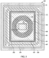
- FIG. 5 is an exemplary layout for a multiple coil structure 500 including multiple loop antennas, charging coils, and ferrite structures for supporting multiple types of wireless charging and near field communications, in accordance with at least a further embodiment.
- the coil structures are substantially the same as the structure illustrated in FIG. 4 .
- the further embodiment provides a still further approach to providing supportive ferrite elements.
- FIG. 4 included a structure having two ferrite elements
- FIG. 5 represents an embodiment which includes four ferrite elements.
- a first ferrite element 424 is similar to the first ferrite element discussed in FIG. 4 , which is associated with the inner charging coil 402 and the first section 416, of the coil structure 414 for supporting near field communications.
- a second ferrite element 502 is associated with the second section 418, of the coil structure 414 for supporting near field communications.
- a third ferrite element 504 is associated with the outer charging coil 408, and a fourth ferrite element 506 is associated with the third section 420, of the coil structure 414 for supporting near field communications.
- compromises associated with the second ferrite element 426, illustrated in FIG. 4 in connection with supporting both resonant charging and near field communications can be minimized and/or avoided.
- the type of material selected for both the second 502 and fourth 506 ferrite element can be the same or substantially similar.
- FIGS. 6 and 7 are partial exemplary layouts for a multiple coil structure including ferrite structures and at least one loop antenna portion for supporting near field communication and at least one charging coil portion for supporting wireless charging, in accordance with at least one embodiment. More specifically, the ferrite structures are associated with the inner charging coil 402 and the first section 416 of the coil structure 414 for supporting near field communications. In each instance, a pair of ferrite structures 602 and 604 are shown, relative to this portion of the multiple coil structure. In FIG. 6 , the second ferrite element 604 is shown inset into an internal cut out or opening in the first ferrite element 602. Alternatively, in FIG. 7 , the second ferrite element 704 is shown stacked on top of the first ferrite element 702, where in FIG.
- the first ferrite element does not have a cut out or opening within which the first ferrite element can be received.
- a more customized or tuned ferrite structure can be provided which supports the alternative operational requirements of the inductive charging of the inner charging coil, relative to the near field communication of the first section 416 of the coil structure 414.
Landscapes
- Engineering & Computer Science (AREA)
- Power Engineering (AREA)
- Computer Networks & Wireless Communication (AREA)
- Signal Processing (AREA)
- Charge And Discharge Circuits For Batteries Or The Like (AREA)
- Coils Or Transformers For Communication (AREA)
- Near-Field Transmission Systems (AREA)
Abstract
Description
- The present invention relates generally to portable electronic devices and the manner in which multiple coils are integrated in a similar space, and more particularly, to portable electronic devices which include respective coils for multiple types of wireless charging, as well as near field communications.
- Wireless charging of portable electronic devices is a feature that is increasingly being supported. While the technology has not yet been widely adopted, we are already starting to see the development of new forms of the technology, which have varying interface requirements. This creates challenges for device manufacturers, that need to decide how they are going to support a particular feature. More specifically, do you support the newer technology, the older technology, or both. If you shift your support to the newer technology, customers that adopted the older technology may be frustrated that previous charging investments may no longer be supported. In some cases, they may not be aware of the fact that there are multiple technologies, and that their new device may not function with their old charger, or vice versa. Consequently, there may be a motivation for manufacturers of wireless charging solutions to support multiple forms of a feature including both newer and older forms of a technology.
- Still further, there is an incentive to try and make the experience associated with the same type of activity as similar as possible even though it may involve different forms of the technology, as users tend to develop habits in line with certain types of tasks. Correspondingly, there may be a motivation to try and co-locate disparate solutions including the operation and interface related to similar activities even if they use different technologies.
- Another factor is the limited amount of device space available for supporting different types of device interactions. So, an ability to co-locate disparate solutions for related types of activities may be beneficial. Still further, given the limited device interface space, there may be a further desire to be able to co-locate still further forms of device interactions, such as support for near field communications proximate support for wireless charging solutions. At least one relatively widely accepted solution has placed support for near field communications proximate the back surface of the device. Similarly, at least some forms of wireless charging have also tended to interact with a device through the back surface of the device.
- The present inventors have correspondingly recognized that coil designs that are adapted to solutions which integrate support for both near field communications, as well as multiple forms of wireless charging in the same or similar space would be beneficial.
- The present invention provides a multiple coil structure for supporting multiple types of wireless charging and near field communications. The multiple coil structure includes an inner charging coil comprising a first conductor path forming one or more loops, wherein the direction of travel of the conductor path from an end point of the first conductor path is one of a substantially clockwise direction or a substantially counter-clockwise direction, and wherein the inner charging coil has an inner boundary and an outer boundary. The multiple coil structure further includes an outer charging coil comprising a second conductor path forming one or more loops, which extend around the outer boundary of the inner charging coil, wherein the direction of travel of the conductor path from an end point of the second conductor path is one of a substantially clockwise direction or a substantially counter-clockwise direction, and wherein the outer charging coil has an inner boundary and an outer boundary. The multiple coil structure still further includes a near field communication coil comprising a third conductor path forming one or more loops within the inner boundary of the inner charging coil, wherein the direction of travel of the conductor path from an end point of the third conductor path is one of a substantially clockwise direction or a substantially counter-clockwise direction.
- In at least one embodiment, the third conductor path in addition to forming one or more loops within the inner boundary of the inner charging coil includes a section of conductor path that transitions to an area outside the outer boundary of the inner charging coil and inside the inner boundary of the outer charging coil, where the third conductor path includes one or more additional loops in substantially the same direction as the loops formed by the third conductor path within the inner boundary of the inner charging coil.
- In at least a further embodiment, the third conductor path in addition to forming one or more loops within the inner boundary of the inner charging coil includes a section of conductor path that transitions to an area outside the outer boundary of the outer charging coil, where the third conductor path includes one or more additional loops in substantially the same direction as the loops formed by the third conductor path within the inner boundary of the inner charging coil.
- The present invention further provides portable electronic device having wireless charging capabilities and near field communication capabilities. The portable electronic device includes a power storage element, one or more wireless charging circuits coupled to the power storage element, and a near field communication transceiver. The portable electronic device further includes a multiple coil structure. The multiple coil structure includes an inner charging coil comprising a first conductor path forming one or more loops, wherein the direction of travel of the conductor path from an end point of the first conductor path is one of a substantially clockwise direction or a substantially counter-clockwise direction, and wherein the inner charging coil has an inner boundary and an outer boundary. The multiple coil structure further includes an outer charging coil comprising a second conductor path forming one or more loops, which extend around the outer boundary of the inner charging coil, wherein the direction of travel of the conductor path from an end point of the second conductor path is one of a substantially clockwise direction or a substantially counter-clockwise direction, and wherein the outer charging coil has an inner boundary and an outer boundary. The multiple coil structure still further includes a near field communication coil comprising a third conductor path forming one or more loops within the inner boundary of the inner charging coil, wherein the direction of travel of the conductor path from an end point of the third conductor path is one of a substantially clockwise direction or a substantially counter-clockwise direction.
- These and other objects, features, and advantages of this invention are evident from the following description of one or more preferred embodiments of this invention, with reference to the accompanying drawings.
-
-
FIG. 1 is a front view of an exemplary hand held electronic device; -
FIG. 2 is a back view of an exemplary hand held electronic device, which could correspond to the hand held electronic device illustrated inFIG. 1 ; -
FIG. 3 is a block diagram of a hand held electronic device in accordance with at least one embodiment; -
FIG. 4 is an exemplary layout for a multiple coil structure including multiple loop antennas, charging coils, and ferrite structures for supporting multiple types of wireless charging and near field communications, in accordance with at least one embodiment; -
FIG. 5 is an exemplary layout for a multiple coil structure including multiple loop antennas, charging coils, and ferrite structures for supporting multiple types of wireless charging and near field communications, in accordance with at least a further embodiment; -
FIG. 6 is a partial exemplary layout for a multiple coil structure including ferrite structures and at least one loop antenna portion for supporting near field communication and at least one charging coil portion for supporting wireless charging, in accordance with at least one embodiment; and -
FIG. 7 is a partial exemplary layout for a multiple coil structure including ferrite structures and at least one loop antenna portion for supporting near field communication and at least one charging coil portion for supporting wireless charging, in accordance with at least a further embodiment. - While the present invention is susceptible of embodiment in various forms, there is shown in the drawings and will hereinafter be described presently preferred embodiments with the understanding that the present disclosure is to be considered an exemplification of the invention and is not intended to limit the invention to the specific embodiments illustrated. One skilled in the art will hopefully appreciate that the elements in the drawings are illustrated for simplicity and clarity and have not necessarily been drawn to scale. For example, the dimensions of some of the elements in the drawings may be exaggerated relative to other elements with the intent to help improve understanding of the aspects of the embodiments being illustrated and described.
-
FIG. 1 illustrates a front view of an exemplary hand heldelectronic device 100. While in the illustrated embodiment, the type of hand held electronic device shown is a radio frequency cellular telephone, which incorporates near field communication capabilities and wireless charging capabilities, other types of devices that incorporate near field communication capabilities and wireless charging capabilities are also relevant to the present application. In other words, the present application is generally applicable to hand held electronic devices beyond the type being specifically shown. A couple of additional examples of suitable hand held electronic devices that may additionally be relevant to the present application in the incorporation and management of multiple types of wireless charging and near field communications in a hand held electronic device can include a tablet, a cordless telephone, a selective call receiver, an audio player, a gaming device, a personal digital assistant, as well as any other form of hand held electronic device that one might at least sometimes carry around on one's person for which it might be desirable to wirelessly charge and/or engage in one or more forms of near field communications. - In the illustrated embodiment, the radio frequency cellular telephone includes a
display 102 which covers a large portion of the front facing. In at least some instances, the display can incorporate a touch sensitive matrix, that facilitates detection of one or more user inputs relative to at least some portions of the display, including interaction with visual elements being presented to the user via thedisplay 102. In some instances, the visual element could be an object with which the user can interact. In other instances, the visual element can form part of a visual representation of a keyboard including one or more virtual keys and/or one or more buttons with which the user can interact and/or select for actuation. In addition to one or more virtual user actuatable buttons or keys, thedevice 100 can include one or more physical useractuatable buttons 104. In the particular embodiment illustrated, the device has three such buttons located along the right side of the device. - The exemplary hand held electronic device, illustrated in
FIG. 1 , additionally includes aspeaker 106 and amicrophone 108 in support of voice communications. Thespeaker 106 may additionally support the reproduction of an audio signal, which could be a stand-alone signal, such as for use in the playing of music, or can be part of a multimedia presentation, such as for use in the playing of a movie, which might have at least an audio as well as a visual component. The speaker may also include the capability to also produce a vibratory effect. However, in some instances, the purposeful production of vibrational effects may be associated with a separate element, not shown, which is internal to the device. Generally, the speaker is located toward the top of the device, which corresponds to an orientation consistent with the respective portion of the device facing in an upward direction during usage in support of a voice communication. In such an instance, thespeaker 106 might be intended to align with the ear of the user, and themicrophone 108 might be intended to align with the mouth of the user. Also located near the top of the device, in the illustrated embodiment, is a front facingcamera 110. -
FIG. 2 illustrates a back view of the exemplary hand heldelectronic device 100, illustrated inFIG. 1 . In the back view of the exemplary hand held electronic device, the three physical useractuatable buttons 104, which are visible in the front view, can similarly be seen. The exemplary hand held electronic device additionally includes a backside facing camera 202 with aflash 204, as well as a serial bus port 206, which is generally adapted for receiving a cable connection, which can be used to receive data and/or power signals. Still further, the illustrated embodiment includes anarea 210 proximate the back side surface, within which one or more loop antennas for supporting such functions as near field communications and/or wireless charging. The one or more loop antennas can be located internal to the device, often just below the back side surface of thedevice 100. -
FIG. 3 illustrates a block diagram 300 of a hand heldelectronic device 100, in accordance with at least one embodiment. In the illustrated embodiment, the hand heldelectronic device 100 includes acontroller 302, which is adapted for managing at least some of the operation of thedevice 100. In some embodiments, thecontroller 302 could be implemented in the form of one or more microprocessors, which are adapted to execute one or more sets ofpre-stored instructions 304, which may be used to form or implement the operation of at least part of one or more controller modules. The one or more sets ofpre-stored instructions 304 may be stored in astorage element 306, which while shown as being integrated as part of thecontroller 302, may additionally or alternatively include some data storage capability for storing at least some of the prestored instructions for use with thecontroller 302, that are separate from and coupled to thecontroller 302. - The
storage element 306 could include one or more forms of volatile and/or non-volatile memory, including conventional ROM, EPROM, RAM, or EEPROM. The possible additional data storage capabilities may also include one or more forms of auxiliary storage, which is either fixed or removable, such as a hard drive, a floppy drive, or a memory stick. One skilled in the art will still further appreciate that still other further forms of storage elements could be used without departing from the teachings of the present disclosure. In the same or other instances, thecontroller 302 may additionally or alternatively incorporate state machines and/or logic circuitry, which can be used to implement at least partially, some of the modules and/or functionality associated with thecontroller 302. - In the illustrated embodiment, the device further includes one or
more transceivers 308, which are coupled to thecontroller 302 and which serve to manage the external communication of data including their wireless communication using one or more forms of communications. In such an instance, the transceivers will generally each be coupled to acorresponding antenna 310 via which the wireless communication signals will be radiated and received. For example, the one ormore transceivers 308 might include a receiver for supporting communications with a global positioning system, a transceiver for supporting cellular radio frequency communications, a transceiver for supporting Bluetooth® type communications, as well as a transceiver for supporting Wi-Fi® type communications. Transceivers for other forms of communication are additionally and/or alternatively possible. While each transceiver is often associated with a separate antenna, it is possible that some antennas may be able to support multiple forms of communication, as well as potentially some forms of near field communication. For example, in at least some instances, it is envisioned that an antenna that supports cellular communications may also support a single turn loop antenna design for use with some forms of near field communications including near field communications that might support and make use of active load modulation. - In addition to the one or
more transceivers 308, thedevice 100 additionally includes near fieldcommunication control circuitry 312, which is coupled torespective antenna structure 314 for supporting near field communications. In at least some instances, chipsets may be available, which providecontrol circuitry 312 for supporting near field communications. - Still further, the hand held electronic device further includes a
power storage element 316, such as a battery, capacitor or other such device for storing energy, which can be later used to provide electric power to the other circuit elements. In conjunction with being able to supply power to other circuit elements, the power storage element is able to receive power with at least some of the received power being available for later distribution. In at least some instances, the power received by the power storage element will be received from one or more charging circuits, such as one or morewireless charging circuits 318, as well as one or more wired connections, such as the previously noted serial bus port 206. In the illustrated embodiment, thedevice 100 can include at least a pair ofwireless charging circuits respective charging loops - The charging loops are intended to couple either inductively or via a loosely coupled magnetic resonance to another corresponding related coil external to the
device 100, which is properly tuned, whereby a change in current produced in a first one of the corresponding related coils will interact with the other related coil through an electromagnetic field, so as to induce a change in current in the other related coil. The induced change in current produced in the corresponding related coil can be used by the corresponding wireless charging circuit to produce power that can be used to power the electronic circuitry contained in the hand held electronic device, and/or supply power to or replenish power in thepower storage element 316, which can be later used to supply power to the electronic circuitry of the hand held electronic device. - In the illustrated embodiment, the charging
loops antenna 314 associated with the near fieldcommunication control circuitry 312. The chargingloops antenna 314, in at least some instances, form concentric loops which generally support communications and/or wireless charging proximate a common single portion of the surface area of the device. The common single portion of the surface area of the device, includes the one or more related charging loops and antennas being located at or near an external surface of the device, where in the illustrated embodiment, the respective loop structures are located just below aportion 210 of the external back surface of thedevice 100. - In the illustrated embodiment, the
device 100 can additionally includeuser interface circuitry 328. For example, theuser interface circuitry 328 can include adisplay 102, which may further support a touchsensitive array 330. The user interface circuitry may also include aspeaker 106, amicrophone 108, one or more user actuatable switches 104, avibrational element 332, and one ormore cameras -
FIG. 4 illustrates an exemplary layout for amultiple coil structure 400 including multiple loop antennas, charging coils, and ferrite structures for supporting multiple types of wireless charging and near field communications, in accordance with at least one embodiment. More specifically, themultiple coil structure 400 includes aninner charging coil 402 comprised of a conductor path forming one or more loops. Generally, the loops will extend from one of two ends to the second of two ends in the same one of a clockwise or a counter-clockwise direction. For example, in the illustrated embodiment, the corresponding loops of the inner charging coil are seen as extending in a clockwise direction when viewed from theend 404 corresponding to the inside most loop to theend 406 corresponding to the outside most loop. The loops of theinner charging coil 402 are configured and dimensioned to have at least a desired degree of resonance with a coil associated with a separate external charger structure. Together, theinner charging coil 402 and the coil associated with a separate charger structure inductively couple to allow an electric current conveyed through the coil associated with the separate charger structure to induce an electric current in theinner charging coil 402 of thedevice 100. - The
multiple coil structure 400 additionally includes anouter charging coil 408, which is located in an area outside of an outer boundary of theinside charging coil 402. Theouter charging coil 408 similarly extends from one of twoends 410 in one of a clockwise or a counter-clockwise direction. By having a pair ofcrossover points 412 in the three loop structure, it is possible for the loop to have both of itsends 410 be located on the same outer side of the loop structure. The crossover can include a pair of vias and connecting conductor present on a different layer of the substrate upon which the conductor paths are located. It is also possible, that a wire conductor that can extend out of the planar layer of the substrate, which has respective ends coupled to alternative ones of a pair of through holes or mounting pads, which can traverse the in-plane trace conductor in a layer of the substrate and allow a crossing of the in-plane trace conductor without shorting to the same. Similar to theinner charging coil 402, The loops of theouter charging coil 408 are configured and dimensioned to have at least a desired degree of resonance with a coil associated with a separate external charger structure. Together, theouter charging coil 408 and the coil associated with a separate charger structure magnetically couple to allow an electric current conveyed through the coil associated with the separate charger structure to induce an electric current in theouter charging coil 408 of thedevice 100. - In the illustrated embodiment, the inner charging coil can be associated with a form of wireless charging often referred to as inductive wireless charging following one or more of at least two wireless standards including WPC (Wireless Power Consortium) Inductive, and PMA (Power Matters Alliance) Inductive. Such a charging type generally operates between 100kHz and 300kHz, and currently supports a transmitter power on the order of around 5W. The outer charging coil, in the illustrated embodiment, can be associated with a form of wireless charging often referred to as resonant wireless charging, which could correspond to and/or include a wireless charging standard, such as A4WP (Alliance for Wireless Power) Resonant. The identified resonant wireless charging standard operates at a frequency between 6MHz and 7MHz, and currently supports a transmitter power on the order of around 16W. The resonant wireless charging standard further benefits from greater freedom of positioning of the two inductively coupled coils via which the power is transferred, and sometimes can include a bowl type structure within which the device to be charged can be received, as opposed to or in addition to a surface upon which a properly positioned and aligned device can be received.
- In the illustrated embodiment, the
multiple coil structure 400 still further includes acoil structure 414 for supporting near field communications. Thecoil structure 414 for supporting near field communications can include one or more sections. In the illustrated embodiment, thecoil structure 414 includes three sections. Afirst section 416 includes the portion of thecoil structure 414 that is located in the area inside an inner boundary area of theinner charging coil 402. Asecond section 418 includes the portion of thecoil structure 414 that is located between the area outside of the outer boundary area of theinner charging coil 402, and inside the inner boundary area of theouter charging coil 408. Athird section 420 includes the portion of thecoil structure 414 that is located in the area outside the outer boundary area of theouter charging coil 408. Similar to theinner charging coil 402 and theouter charging coil 408, the coil structure generally follows one of a clockwise or a counter-clockwise direction as the conductor forming the coil structure extends between twoends 422 depending upon which end you start from. - The three sections of the
coil structure 414 for supporting near field communications, illustrated inFIG. 4 are each adapted for targeting a different type of near field communications. For example, thefirst section 416, or inner portion, is adapted to better interact with near field communication tags including tags associated with accessory devices, such as Bluetooth® headsets. The corresponding near field communications between the accessory and the device can in turn help support a pairing of the accessory with thedevice 100. In at least some instances, thefirst section 416, or inner portion, will have coil diameters consistent with a range between approximately 10mm and 15mm. Thesecond section 418, or middle portion, is adapted to better interact with forms of near field communication associated with payment terminals. In at least some instances, thesecond section 418 will have coil diameters consistent with a range between approximately 45mm and 50mm. Thethird section 420, or outer portion, is adapted to better interact with near field communications associated with readers in transportation systems. In at least some instances, thethird section 420 will have coil diameters consistent with a range between approximately 60mm and 65mm. - The
multiple coil structure 400 can additionally include one or more ferrite elements, that are proximate one or more of the various coils, which are included as part of the multiple coil structure. The multiple coils as part of their inductive coupling will have an associated magnetic field. The ferrite elements are intended to provide a tuned return path, which is intended to help steer the location and direction of the corresponding field lines. In selecting the nature of the ferrite elements, one looks at magnetic permeability of the ferrite material at various frequencies of interest. In some instances the corresponding ferrite element can be associated with multiple coils, where each of the associated coils will have differing geometries as well as differing frequencies of operation. In such an instance, it may be necessary to make compromises relative to the features of the ferrite element to support potentially varying operational characteristics of the multiple associated coils. - In the illustrated embodiment, the
multiple coil structure 400 includes afirst ferrite element 424 associated with theinner charging coil 402 and thefirst section 416, of thecoil structure 414 for supporting near field communications. Thefirst ferrite element 424 in the exemplary embodiment is associated with a first hatched area. Asecond ferrite element 426 is associated with theouter charging coil 408, as well as the second 418 and third 420 sections of thecoil structure 414 for supporting near field communications. Thesecond ferrite element 426 is associated with an a second hatched area. In the illustrated embodiment, thefirst ferrite element 424 takes into account the features of inductive charging associated with the inner charging coil in selecting the type of material, as well as the size and thickness of the material used. Thesecond ferrite element 426 takes into account the features associated with resonant charging, as well as at least some aspects of the near field communications in selecting the type of material, as well as the size and thickness of the material used. -
FIG. 5 is an exemplary layout for amultiple coil structure 500 including multiple loop antennas, charging coils, and ferrite structures for supporting multiple types of wireless charging and near field communications, in accordance with at least a further embodiment. In the embodiment illustrated inFIG. 5 , the coil structures are substantially the same as the structure illustrated inFIG. 4 . However, the further embodiment provides a still further approach to providing supportive ferrite elements. WhileFIG. 4 included a structure having two ferrite elements,FIG. 5 represents an embodiment which includes four ferrite elements. In this alternative embodiment, afirst ferrite element 424 is similar to the first ferrite element discussed inFIG. 4 , which is associated with theinner charging coil 402 and thefirst section 416, of thecoil structure 414 for supporting near field communications. Asecond ferrite element 502 is associated with thesecond section 418, of thecoil structure 414 for supporting near field communications. Athird ferrite element 504 is associated with theouter charging coil 408, and afourth ferrite element 506 is associated with thethird section 420, of thecoil structure 414 for supporting near field communications. In this way compromises associated with thesecond ferrite element 426, illustrated inFIG. 4 , in connection with supporting both resonant charging and near field communications can be minimized and/or avoided. In at least some instances, the type of material selected for both the second 502 and fourth 506 ferrite element can be the same or substantially similar. -
FIGS. 6 and7 are partial exemplary layouts for a multiple coil structure including ferrite structures and at least one loop antenna portion for supporting near field communication and at least one charging coil portion for supporting wireless charging, in accordance with at least one embodiment. More specifically, the ferrite structures are associated with theinner charging coil 402 and thefirst section 416 of thecoil structure 414 for supporting near field communications. In each instance, a pair offerrite structures FIG. 6 , thesecond ferrite element 604 is shown inset into an internal cut out or opening in thefirst ferrite element 602. Alternatively, inFIG. 7 , thesecond ferrite element 704 is shown stacked on top of thefirst ferrite element 702, where inFIG. 7 , the first ferrite element does not have a cut out or opening within which the first ferrite element can be received. In these ways, a more customized or tuned ferrite structure can be provided which supports the alternative operational requirements of the inductive charging of the inner charging coil, relative to the near field communication of thefirst section 416 of thecoil structure 414. - While the preferred embodiments of the invention have been illustrated and described, it is to be understood that the invention is not so limited. Numerous modifications, changes, variations, substitutions and equivalents will occur to those skilled in the art without departing from the spirit and scope of the present invention as defined by the appended claims.
Further aspects of the invention are provided by the subject matter of the following clauses: - 1. A multiple coil structure for supporting multiple types of charging and near field communications comprising:
- an inner charging coil comprising a first conductor path forming one or more loops, wherein the direction of travel of the conductor path from an end point of the first conductor path is one of a substantially clockwise direction or a substantially counter-clockwise direction, and wherein the inner charging coil has an inner boundary and an outer boundary;
- an outer charging coil comprising a second conductor path forming one or more loops, which extend around the outer boundary of the inner charging coil, wherein the direction of travel of the conductor path from an end point of the second conductor path is one of a substantially clockwise direction or a substantially counter-clockwise direction, and wherein the outer charging coil has an inner boundary and an outer boundary; and
- a near field communication coil comprising a third conductor path forming one or more loops within the inner boundary of the inner charging coil, wherein the direction of travel of the conductor path from an end point of the third conductor path is one of a substantially clockwise direction or a substantially counter-clockwise direction.
- 2. A multiple coil structure in accordance with clause 1, wherein the third conductor path in addition to forming one or more loops within the inner boundary of the inner charging coil includes a section of conductor path that transitions to an area outside the outer boundary of the inner charging coil and inside the inner boundary of the outer charging coil, where the third conductor path includes one or more additional loops in substantially the same direction as the loops formed by the third conductor path within the inner boundary of the inner charging coil.
- 3. A multiple coil structure in accordance with clause 1 or clause 2, wherein the third conductor path in addition to forming one or more loops within the inner boundary of the inner charging coil includes a section of conductor path that transitions to an area outside the outer boundary of the outer charging coil, where the third conductor path includes one or more additional loops in substantially the same direction as the loops formed by the third conductor path within the inner boundary of the inner charging coil.
- 4. A multiple coil structure in accordance with clause 1, wherein the third conductor path in addition to forming one or more loops within the inner boundary of the inner charging coil includes a section of conductor path that transitions to an area outside the outer boundary of the inner charging coil and inside the inner boundary of the outer charging coil, where the third conductor path includes one or more additional loops in substantially the same direction as the loops formed by the third conductor path within the inner boundary of the inner charging coil; and wherein the third conductor path includes a section of conductor path that transitions to an area outside the outer boundary of the outer charging coil, where the third conductor path includes one or more additional loops in substantially the same direction as the loops formed by the third conductor path within the inner boundary of the inner charging coil.
- 5. A multiple coil structure in accordance with any of clauses 1 to 4, further comprising:
- a first ferrite, which is positioned beneath the respective coils and portions thereof found in the area which encompasses the inner charging coil, and the portion of the near field communication coil located within the inner boundary of the inner charging coil; and
- a second ferrite of a type different than the first ferrite, where the second ferrite is positioned beneath the respective coils and portions thereof found in the area which encompasses the outer charging coil, and the portion of the near field communication coil located outside the outer boundary of the inner charging coil.
- 6. A multiple coil structure in accordance with any of clauses 1 to 5, further comprising:
- a first ferrite, which is positioned beneath the respective coils and portions thereof found in the area which encompasses the inner charging coil, and the portion of the near field communication coil located within the inner boundary of the inner charging coil;
- a second ferrite of a type different than the first ferrite, where the second ferrite is positioned beneath the respective coils found in the area which encompasses the outer charging coil;
- a third ferrite of a type different than the first ferrite and the second ferrite, where the third ferrite is positioned beneath the respective coils and portions thereof found in the area which encompasses the portion of the near field communication coil located outside the outer boundary of the inner charging coil and inside the inner boundary of the outer charging coil; and
- a fourth ferrite of a type similar to the third ferrite, where the fourth ferrite is positioned beneath the respective coils and portions thereof found in the area which encompasses the portion of the near field communication coil located outside the outer boundary of the outer charging coil.
- 7. A multiple coil structure in accordance with any of clauses 1 to 6, wherein the portion of the near field communication coil in each respective area is adapted to target a different type of communication.
- 8. A multiple coil structure in accordance with any of clauses 1 to 7, wherein the portion of the near field communication coil located within the inner boundary of the inner charging coil is adapted for interacting with near field communication tags.
- 9. A multiple coil structure in accordance with any of clauses 1 to 8, wherein the portion of the near field communication coil located outside the outer boundary of the inner charging coil and within the inner boundary of the outer charging coil is adapted for interacting with near field communication payment terminals.
- 10. A multiple coil structure in accordance with any of clauses 1 to 9, wherein the portion of the near field communication coil located outside the outer boundary of the outer charging coil is adapted for interacting with near field communication transportation readers.
- 11. A multiple coil structure in accordance with any of clauses 1 to 10, wherein the end points of the first conductor path and the second conductor path, respectively corresponding to the inner charging coil and the outer charging coil, each form terminals for interacting with a corresponding charging circuit.
- 12. A multiple coil structure in accordance with any of clauses 1 to 11, wherein the inner charging coil is an inductive charging coil.
- 13. A multiple coil structure in accordance with any of clauses 1 to 12, wherein the outer charging coil is a resonant charging coil.
- 14. A multiple coil structure in accordance with any of clauses 1 to 13, further comprising:
- a first ferrite, which is positioned beneath the respective coils and portions thereof found in the area which encompasses the inner charging coil; and
- a second ferrite of a type different than the first ferrite, where the second ferrite is positioned beneath the respective coils and portions thereof found in the area of the near field communication coil located within the inner boundary of the inner charging coil.
- 15. A multiple coil structure in accordance with any of clauses 1 to 14, further comprising:
- a first ferrite, which is positioned beneath the respective coils and portions thereof found in the area which encompasses the inner charging coil, and the portion of the near field communication coil located within the inner boundary of the inner charging coil; and
- a second ferrite of a type different than the first ferrite, where the second ferrite is positioned beneath the respective coils and portions thereof found in the area of the near field communication coil located within the inner boundary of the inner charging coil.
- 16. A portable electronic device having wireless charging capabilities and near field communication capabilities, the portable electronic device comprising:
- a power storage element;
- one or more wireless charging circuits coupled to the power storage element;
- a near field communication transceiver; and
- a multiple coil structure including
- an inner charging coil coupled to a corresponding one of the wireless charging circuits, the inner charging coil comprising a first conductor path forming one or more loops, wherein the direction of travel of the conductor path from an end point of the first conductor path is one of a substantially clockwise direction or a substantially counter-clockwise direction, and wherein the inner charging coil has an inner boundary and an outer boundary,
- an outer charging coil coupled to a corresponding one of the wireless charging circuits, the outer charging coil comprising a second conductor path forming one or more loops, which extend around the outer boundary of the inner charging coil, wherein the direction of travel of the conductor path from an end point of the second conductor path is one of a substantially clockwise direction or a substantially counter-clockwise direction, and wherein the outer charging coil has an inner boundary and an outer boundary, and
- a near field communication coil coupled to the near field communication transceiver, the near field communication coil comprising a third conductor path forming one or more loops within the inner boundary of the inner charging coil, wherein the direction of travel of the conductor path from an end point of the third conductor path is one of a substantially clockwise direction or a substantially counter-clockwise direction.
- 17. A portable electronic device in accordance with clause 16, wherein the device includes a front side surface and a back side surface, where the front side surface includes a display, and the multiple coil structure is proximate the back side surface.
- 18. A portable electronic device in accordance with clause 16 or clause 17, wherein the third conductor path of the multiple coil structure in addition to forming one or more loops within the inner boundary of the inner charging coil includes a section of conductor path that transitions to an area outside the outer boundary of the inner charging coil and inside the inner boundary of the outer charging coil, where the third conductor path includes one or more additional loops in substantially the same direction as the loops formed by the third conductor path within the inner boundary of the inner charging coil.
- 19. A portable electronic device in accordance with clause 16 or clause 17, wherein the third conductor path of the multiple coil structure in addition to forming one or more loops within the inner boundary of the inner charging coil includes a section of conductor path that transitions to an area outside the outer boundary of the outer charging coil, where the third conductor path includes one or more additional loops in substantially the same direction as the loops formed by the third conductor path within the inner boundary of the inner charging coil.
- 20. A portable electronic device in accordance with clause 16 or clause 17, wherein the third conductor path of the multiple coil structure in addition to forming one or more loops within the inner boundary of the inner charging coil includes a section of conductor path that transitions to an area outside the outer boundary of the inner charging coil and inside the inner boundary of the outer charging coil, where the third conductor path includes one or more additional loops in substantially the same direction as the loops formed by the third conductor path within the inner boundary of the inner charging coil; and wherein the third conductor path includes a section of conductor path that transitions to an area outside the outer boundary of the outer charging coil, where the third conductor path includes one or more additional loops in substantially the same direction as the loops formed by the third conductor path within the inner boundary of the inner charging coil.
Claims (15)
- A multiple coil structure for supporting multiple types of charging and near field communications comprising:an inner charging coil comprising a first conductor path forming one or more loops, wherein the direction of travel of the conductor path from an end point of the first conductor path is one of a substantially clockwise direction or a substantially counter-clockwise direction, and wherein the inner charging coil has an inner boundary and an outer boundary;an outer charging coil comprising a second conductor path forming one or more loops, which extend around the outer boundary of the inner charging coil, wherein the direction of travel of the conductor path from an end point of the second conductor path is one of a substantially clockwise direction or a substantially counter-clockwise direction, and wherein the outer charging coil has an inner boundary and an outer boundary; anda near field communication coil comprising a third conductor path forming one or more loops within the inner boundary of the inner charging coil, wherein the direction of travel of the conductor path from an end point of the third conductor path is one of a substantially clockwise direction or a substantially counter-clockwise direction.
- A multiple coil structure in accordance with claim 1, wherein the third conductor path in addition to forming one or more loops within the inner boundary of the inner charging coil includes a section of conductor path that transitions to an area outside the outer boundary of the inner charging coil and inside the inner boundary of the outer charging coil, where the third conductor path includes one or more additional loops in substantially the same direction as the loops formed by the third conductor path within the inner boundary of the inner charging coil.
- A multiple coil structure in accordance with claim 1 or claim 2, wherein the third conductor path in addition to forming one or more loops within the inner boundary of the inner charging coil includes a section of conductor path that transitions to an area outside the outer boundary of the outer charging coil, where the third conductor path includes one or more additional loops in substantially the same direction as the loops formed by the third conductor path within the inner boundary of the inner charging coil.
- A multiple coil structure in accordance with claim 1, wherein the third conductor path in addition to forming one or more loops within the inner boundary of the inner charging coil includes a section of conductor path that transitions to an area outside the outer boundary of the inner charging coil and inside the inner boundary of the outer charging coil, where the third conductor path includes one or more additional loops in substantially the same direction as the loops formed by the third conductor path within the inner boundary of the inner charging coil; and wherein the third conductor path includes a section of conductor path that transitions to an area outside the outer boundary of the outer charging coil, where the third conductor path includes one or more additional loops in substantially the same direction as the loops formed by the third conductor path within the inner boundary of the inner charging coil.
- A multiple coil structure in accordance with any of claims 1 to 4, further comprising:a first ferrite, which is positioned beneath the respective coils and portions thereof found in the area which encompasses the inner charging coil, and the portion of the near field communication coil located within the inner boundary of the inner charging coil; anda second ferrite of a type different than the first ferrite, where the second ferrite is positioned beneath the respective coils and portions thereof found in the area which encompasses the outer charging coil, and the portion of the near field communication coil located outside the outer boundary of the inner charging coil.
- A multiple coil structure in accordance with any of claims 1 to 5, further comprising:a first ferrite, which is positioned beneath the respective coils and portions thereof found in the area which encompasses the inner charging coil, and the portion of the near field communication coil located within the inner boundary of the inner charging coil;a second ferrite of a type different than the first ferrite, where the second ferrite is positioned beneath the respective coils found in the area which encompasses the outer charging coil;a third ferrite of a type different than the first ferrite and the second ferrite, where the third ferrite is positioned beneath the respective coils and portions thereof found in the area which encompasses the portion of the near field communication coil located outside the outer boundary of the inner charging coil and inside the inner boundary of the outer charging coil; anda fourth ferrite of a type similar to the third ferrite, where the fourth ferrite is positioned beneath the respective coils and portions thereof found in the area which encompasses the portion of the near field communication coil located outside the outer boundary of the outer charging coil.
- A multiple coil structure in accordance with any of claims 1 to 6, wherein the portion of the near field communication coil in each respective area is adapted to target a different type of communication.
- A multiple coil structure in accordance with any of claims 1 to 7, wherein the portion of the near field communication coil located within the inner boundary of the inner charging coil is adapted for interacting with near field communication tags.
- A multiple coil structure in accordance with any of claims 1 to 8, wherein the portion of the near field communication coil located outside the outer boundary of the inner charging coil and within the inner boundary of the outer charging coil is adapted for interacting with near field communication payment terminals.
- A multiple coil structure in accordance with any of claims 1 to 9, wherein the portion of the near field communication coil located outside the outer boundary of the outer charging coil is adapted for interacting with near field communication transportation readers.
- A multiple coil structure in accordance with any of claims 1 to 10, wherein the end points of the first conductor path and the second conductor path, respectively corresponding to the inner charging coil and the outer charging coil, each form terminals for interacting with a corresponding charging circuit.
- A multiple coil structure in accordance with any of claims 1 to 11, wherein the inner charging coil is an inductive charging coil, and the outer charging coil is a resonant charging coil.
- A multiple coil structure in accordance with any of claims 1 to 12, further comprising:a first ferrite, which is positioned beneath the respective coils and portions thereof found in the area which encompasses the inner charging coil; anda second ferrite of a type different than the first ferrite, where the second ferrite is positioned beneath the respective coils and portions thereof found in the area of the near field communication coil located within the inner boundary of the inner charging coil.
- A multiple coil structure in accordance with any of claims 1 to 13, further comprising:a first ferrite, which is positioned beneath the respective coils and portions thereof found in the area which encompasses the inner charging coil, and the portion of the near field communication coil located within the inner boundary of the inner charging coil; anda second ferrite of a type different than the first ferrite, where the second ferrite is positioned beneath the respective coils and portions thereof found in the area of the near field communication coil located within the inner boundary of the inner charging coil.
- A portable electronic device having wireless charging capabilities and near field communication capabilities, the portable electronic device comprising:a power storage element;one or more wireless charging circuits coupled to the power storage element;a near field communication transceiver; anda multiple coil structure includingan inner charging coil coupled to a corresponding one of the wireless charging circuits, the inner charging coil comprising a first conductor path forming one or more loops, wherein the direction of travel of the conductor path from an end point of the first conductor path is one of a substantially clockwise direction or a substantially counter-clockwise direction, and wherein the inner charging coil has an inner boundary and an outer boundary,an outer charging coil coupled to a corresponding one of the wireless charging circuits, the outer charging coil comprising a second conductor path forming one or more loops, which extend around the outer boundary of the inner charging coil, wherein the direction of travel of the conductor path from an end point of the second conductor path is one of a substantially clockwise direction or a substantially counter-clockwise direction, and wherein the outer charging coil has an inner boundary and an outer boundary, anda near field communication coil coupled to the near field communication transceiver, the near field communication coil comprising a third conductor path forming one or more loops within the inner boundary of the inner charging coil, wherein the direction of travel of the conductor path from an end point of the third conductor path is one of a substantially clockwise direction or a substantially counter-clockwise direction.
Applications Claiming Priority (1)
| Application Number | Priority Date | Filing Date | Title |
|---|---|---|---|
| US14/835,149 US9825484B2 (en) | 2015-08-25 | 2015-08-25 | Multiple coil structure for supporting multiple types of wireless charging and near field communications |
Publications (2)
| Publication Number | Publication Date |
|---|---|
| EP3136543A1 true EP3136543A1 (en) | 2017-03-01 |
| EP3136543B1 EP3136543B1 (en) | 2018-05-09 |
Family
ID=56851397
Family Applications (1)
| Application Number | Title | Priority Date | Filing Date |
|---|---|---|---|
| EP16185016.9A Active EP3136543B1 (en) | 2015-08-25 | 2016-08-19 | A multiple coil structure for supporting multiple types of wireless charging and near field communications |
Country Status (3)
| Country | Link |
|---|---|
| US (1) | US9825484B2 (en) |
| EP (1) | EP3136543B1 (en) |
| JP (1) | JP6343861B2 (en) |
Cited By (2)
| Publication number | Priority date | Publication date | Assignee | Title |
|---|---|---|---|---|
| CN107276255A (en) * | 2017-06-30 | 2017-10-20 | 努比亚技术有限公司 | A kind of wireless charger and its charge control method |
| EP3843241A1 (en) * | 2019-12-24 | 2021-06-30 | Guangdong Oppo Mobile Telecommunications Corp., Ltd. | Electronic device |
Families Citing this family (16)
| Publication number | Priority date | Publication date | Assignee | Title |
|---|---|---|---|---|
| TWI613686B (en) | 2012-03-23 | 2018-02-01 | Lg伊諾特股份有限公司 | Method of manufacturing a wireless power receiver |
| JP6313744B2 (en) | 2012-03-23 | 2018-04-18 | エルジー イノテック カンパニー リミテッド | Wireless power receiver |
| KR20160103471A (en) * | 2015-02-24 | 2016-09-01 | 삼성전자주식회사 | Electronic device and method for correcting a position of electronic device |
| DE112015006580T5 (en) * | 2015-06-04 | 2018-05-24 | Intel Corporation | Coil configuration in a wireless power transmitter |
| WO2017031348A1 (en) | 2015-08-19 | 2017-02-23 | Nucurrent, Inc. | Multi-mode wireless antenna configurations |
| KR20170050656A (en) * | 2015-10-30 | 2017-05-11 | 삼성전자주식회사 | Wireless power receiver and method for controlling thereof |
| KR102572577B1 (en) * | 2016-04-15 | 2023-08-30 | 삼성전자주식회사 | Charging apparatus and method for controlling wireless charging |
| GB2562447A (en) * | 2016-12-22 | 2018-11-21 | Bombardier Primove Gmbh | A secondary-sided arrangement of winding structures and a method for manufacturing a secondary sided arrangement |
| US10469119B2 (en) | 2017-05-25 | 2019-11-05 | Spigen Korea Co., Ltd. | Magnetic mount for electronic devices |
| US12191902B2 (en) | 2017-05-25 | 2025-01-07 | Spigen Korea Co., Ltd. | Mobile electronic device cases for electromagnetic shielding |
| US12224788B2 (en) | 2017-05-25 | 2025-02-11 | Spigen Korea Co., Ltd. | Magnetic auxiliary devices for mobile devices |
| CN107370243B (en) * | 2017-06-20 | 2019-06-07 | 华为技术有限公司 | A kind of terminal wireless charging receiver, emitter and wireless charging system |
| US11018526B2 (en) * | 2018-02-08 | 2021-05-25 | Massachusetts Institute Of Technology | Detuning for a resonant wireless power transfer system including cooperative power sharing |
| CN115133674A (en) * | 2021-03-25 | 2022-09-30 | 北京小米移动软件有限公司 | Wireless charging receiving end and system, and wireless charging control method and device |
| JP7680264B2 (en) * | 2021-05-24 | 2025-05-20 | Tdk株式会社 | Coil component and wireless power transmission device including same |
| CN115566812A (en) * | 2022-09-30 | 2023-01-03 | Oppo广东移动通信有限公司 | Wireless charging coil, wireless charging device and electronic equipment |
Citations (2)
| Publication number | Priority date | Publication date | Assignee | Title |
|---|---|---|---|---|
| EP2804290A1 (en) * | 2012-01-09 | 2014-11-19 | KThepower Inc. | Receiver for wireless charging system |
| US20140375262A1 (en) * | 2012-02-17 | 2014-12-25 | Panasonic Corporation | Wireless charging module and mobile terminal provided with same |
Family Cites Families (5)
| Publication number | Priority date | Publication date | Assignee | Title |
|---|---|---|---|---|
| JP5372610B2 (en) | 2009-06-08 | 2013-12-18 | Necトーキン株式会社 | Non-contact power transmission device |
| KR20130024757A (en) * | 2011-08-29 | 2013-03-08 | 주식회사 케이더파워 | The wireless charging system with the different charging ways |
| WO2013157191A1 (en) | 2012-04-17 | 2013-10-24 | パナソニック株式会社 | Coil device and mobile wireless terminal |
| CN109067014B (en) | 2012-09-05 | 2022-04-15 | 瑞萨电子株式会社 | Non-contact charging device |
| WO2015147133A1 (en) | 2014-03-28 | 2015-10-01 | 株式会社村田製作所 | Antenna device and electronic apparatus |
-
2015
- 2015-08-25 US US14/835,149 patent/US9825484B2/en active Active
-
2016
- 2016-08-19 EP EP16185016.9A patent/EP3136543B1/en active Active
- 2016-08-24 JP JP2016163293A patent/JP6343861B2/en active Active
Patent Citations (2)
| Publication number | Priority date | Publication date | Assignee | Title |
|---|---|---|---|---|
| EP2804290A1 (en) * | 2012-01-09 | 2014-11-19 | KThepower Inc. | Receiver for wireless charging system |
| US20140375262A1 (en) * | 2012-02-17 | 2014-12-25 | Panasonic Corporation | Wireless charging module and mobile terminal provided with same |
Cited By (3)
| Publication number | Priority date | Publication date | Assignee | Title |
|---|---|---|---|---|
| CN107276255A (en) * | 2017-06-30 | 2017-10-20 | 努比亚技术有限公司 | A kind of wireless charger and its charge control method |
| EP3843241A1 (en) * | 2019-12-24 | 2021-06-30 | Guangdong Oppo Mobile Telecommunications Corp., Ltd. | Electronic device |
| US11616400B2 (en) | 2019-12-24 | 2023-03-28 | Guangdong Oppo Mobile Telecommunications Corp., Ltd. | Electronic device |
Also Published As
| Publication number | Publication date |
|---|---|
| US20170063128A1 (en) | 2017-03-02 |
| EP3136543B1 (en) | 2018-05-09 |
| JP2017045988A (en) | 2017-03-02 |
| JP6343861B2 (en) | 2018-06-20 |
| US9825484B2 (en) | 2017-11-21 |
Similar Documents
| Publication | Publication Date | Title |
|---|---|---|
| EP3136543B1 (en) | A multiple coil structure for supporting multiple types of wireless charging and near field communications | |
| US9024576B2 (en) | Inductive charging of a rechargeable battery | |
| CN105431993B (en) | Multi-coil wireless power device | |
| US9002264B2 (en) | Antenna structure for a near-field communication device | |
| US20140349572A1 (en) | Integrated inductive power receiver and near field communicator | |
| US8941268B2 (en) | Non-contact power transmission apparatus | |
| US10325708B2 (en) | Spiral near field communication (NFC) antenna coil | |
| US9124303B2 (en) | Apparatus and method for near field communication | |
| US9148190B1 (en) | Multipurpose coils | |
| KR20160026283A (en) | Smart watch for enabling wireless charging | |
| CN103348555B (en) | power delivery | |
| CN112054817A (en) | Mobile terminal | |
| KR101649259B1 (en) | Flexible printed circuit board for wireless communications | |
| JP2012175596A (en) | Portable electronic apparatus | |
| CN105703790B (en) | Mobile terminal | |
| KR101554133B1 (en) | Flexible printed circuit board for wireless communications | |
| KR101554129B1 (en) | Flexible printed circuit board for wireless communications | |
| KR101870877B1 (en) | Antenna structure for mobile apparatus | |
| US11134141B1 (en) | Electronic devices having shared coil structures | |
| CN106663874A (en) | Apparatus and methods for wireless communication | |
| KR101508172B1 (en) | Circuit Board for NFC Antenna with Wireless Charging | |
| CN106663859B (en) | System and method for enabling radio frequency communications for modular mobile electronic devices | |
| US10665937B2 (en) | Antenna system and wireless communication device having a secondary conductive structure which extends into an area forming a loop | |
| CN105556749A (en) | Apparatus and methods for wireless communication | |
| CN112534679B (en) | Device for high frequency near field communication and inductive recharging of portable electronic devices |
Legal Events
| Date | Code | Title | Description |
|---|---|---|---|
| PUAI | Public reference made under article 153(3) epc to a published international application that has entered the european phase |
Free format text: ORIGINAL CODE: 0009012 |
|
| AK | Designated contracting states |
Kind code of ref document: A1 Designated state(s): AL AT BE BG CH CY CZ DE DK EE ES FI FR GB GR HR HU IE IS IT LI LT LU LV MC MK MT NL NO PL PT RO RS SE SI SK SM TR |
|
| AX | Request for extension of the european patent |
Extension state: BA ME |
|
| 17P | Request for examination filed |
Effective date: 20170901 |
|
| RBV | Designated contracting states (corrected) |
Designated state(s): AL AT BE BG CH CY CZ DE DK EE ES FI FR GB GR HR HU IE IS IT LI LT LU LV MC MK MT NL NO PL PT RO RS SE SI SK SM TR |
|
| RIC1 | Information provided on ipc code assigned before grant |
Ipc: H01F 38/14 20060101ALI20180125BHEP Ipc: H02J 50/10 20160101AFI20180125BHEP Ipc: H04B 5/00 20060101ALI20180125BHEP Ipc: H02J 50/27 20160101ALI20180125BHEP |
|
| GRAP | Despatch of communication of intention to grant a patent |
Free format text: ORIGINAL CODE: EPIDOSNIGR1 |
|
| GRAS | Grant fee paid |
Free format text: ORIGINAL CODE: EPIDOSNIGR3 |
|
| INTG | Intention to grant announced |
Effective date: 20180302 |
|
| GRAA | (expected) grant |
Free format text: ORIGINAL CODE: 0009210 |
|
| AK | Designated contracting states |
Kind code of ref document: B1 Designated state(s): AL AT BE BG CH CY CZ DE DK EE ES FI FR GB GR HR HU IE IS IT LI LT LU LV MC MK MT NL NO PL PT RO RS SE SI SK SM TR |
|
| REG | Reference to a national code |
Ref country code: GB Ref legal event code: FG4D |
|
| REG | Reference to a national code |
Ref country code: CH Ref legal event code: EP Ref country code: AT Ref legal event code: REF Ref document number: 998397 Country of ref document: AT Kind code of ref document: T Effective date: 20180515 |
|
| REG | Reference to a national code |
Ref country code: IE Ref legal event code: FG4D |
|
| REG | Reference to a national code |
Ref country code: DE Ref legal event code: R096 Ref document number: 602016002933 Country of ref document: DE |
|
| REG | Reference to a national code |
Ref country code: NL Ref legal event code: MP Effective date: 20180509 |
|
| REG | Reference to a national code |
Ref country code: LT Ref legal event code: MG4D |
|
| PG25 | Lapsed in a contracting state [announced via postgrant information from national office to epo] |
Ref country code: FI Free format text: LAPSE BECAUSE OF FAILURE TO SUBMIT A TRANSLATION OF THE DESCRIPTION OR TO PAY THE FEE WITHIN THE PRESCRIBED TIME-LIMIT Effective date: 20180509 Ref country code: BG Free format text: LAPSE BECAUSE OF FAILURE TO SUBMIT A TRANSLATION OF THE DESCRIPTION OR TO PAY THE FEE WITHIN THE PRESCRIBED TIME-LIMIT Effective date: 20180809 Ref country code: LT Free format text: LAPSE BECAUSE OF FAILURE TO SUBMIT A TRANSLATION OF THE DESCRIPTION OR TO PAY THE FEE WITHIN THE PRESCRIBED TIME-LIMIT Effective date: 20180509 Ref country code: SE Free format text: LAPSE BECAUSE OF FAILURE TO SUBMIT A TRANSLATION OF THE DESCRIPTION OR TO PAY THE FEE WITHIN THE PRESCRIBED TIME-LIMIT Effective date: 20180509 Ref country code: ES Free format text: LAPSE BECAUSE OF FAILURE TO SUBMIT A TRANSLATION OF THE DESCRIPTION OR TO PAY THE FEE WITHIN THE PRESCRIBED TIME-LIMIT Effective date: 20180509 Ref country code: NO Free format text: LAPSE BECAUSE OF FAILURE TO SUBMIT A TRANSLATION OF THE DESCRIPTION OR TO PAY THE FEE WITHIN THE PRESCRIBED TIME-LIMIT Effective date: 20180809 |
|
| PG25 | Lapsed in a contracting state [announced via postgrant information from national office to epo] |
Ref country code: NL Free format text: LAPSE BECAUSE OF FAILURE TO SUBMIT A TRANSLATION OF THE DESCRIPTION OR TO PAY THE FEE WITHIN THE PRESCRIBED TIME-LIMIT Effective date: 20180509 Ref country code: HR Free format text: LAPSE BECAUSE OF FAILURE TO SUBMIT A TRANSLATION OF THE DESCRIPTION OR TO PAY THE FEE WITHIN THE PRESCRIBED TIME-LIMIT Effective date: 20180509 Ref country code: RS Free format text: LAPSE BECAUSE OF FAILURE TO SUBMIT A TRANSLATION OF THE DESCRIPTION OR TO PAY THE FEE WITHIN THE PRESCRIBED TIME-LIMIT Effective date: 20180509 Ref country code: LV Free format text: LAPSE BECAUSE OF FAILURE TO SUBMIT A TRANSLATION OF THE DESCRIPTION OR TO PAY THE FEE WITHIN THE PRESCRIBED TIME-LIMIT Effective date: 20180509 Ref country code: GR Free format text: LAPSE BECAUSE OF FAILURE TO SUBMIT A TRANSLATION OF THE DESCRIPTION OR TO PAY THE FEE WITHIN THE PRESCRIBED TIME-LIMIT Effective date: 20180810 |
|
| REG | Reference to a national code |
Ref country code: AT Ref legal event code: MK05 Ref document number: 998397 Country of ref document: AT Kind code of ref document: T Effective date: 20180509 |
|
| PG25 | Lapsed in a contracting state [announced via postgrant information from national office to epo] |
Ref country code: SK Free format text: LAPSE BECAUSE OF FAILURE TO SUBMIT A TRANSLATION OF THE DESCRIPTION OR TO PAY THE FEE WITHIN THE PRESCRIBED TIME-LIMIT Effective date: 20180509 Ref country code: RO Free format text: LAPSE BECAUSE OF FAILURE TO SUBMIT A TRANSLATION OF THE DESCRIPTION OR TO PAY THE FEE WITHIN THE PRESCRIBED TIME-LIMIT Effective date: 20180509 Ref country code: PL Free format text: LAPSE BECAUSE OF FAILURE TO SUBMIT A TRANSLATION OF THE DESCRIPTION OR TO PAY THE FEE WITHIN THE PRESCRIBED TIME-LIMIT Effective date: 20180509 Ref country code: CZ Free format text: LAPSE BECAUSE OF FAILURE TO SUBMIT A TRANSLATION OF THE DESCRIPTION OR TO PAY THE FEE WITHIN THE PRESCRIBED TIME-LIMIT Effective date: 20180509 Ref country code: AT Free format text: LAPSE BECAUSE OF FAILURE TO SUBMIT A TRANSLATION OF THE DESCRIPTION OR TO PAY THE FEE WITHIN THE PRESCRIBED TIME-LIMIT Effective date: 20180509 Ref country code: DK Free format text: LAPSE BECAUSE OF FAILURE TO SUBMIT A TRANSLATION OF THE DESCRIPTION OR TO PAY THE FEE WITHIN THE PRESCRIBED TIME-LIMIT Effective date: 20180509 Ref country code: EE Free format text: LAPSE BECAUSE OF FAILURE TO SUBMIT A TRANSLATION OF THE DESCRIPTION OR TO PAY THE FEE WITHIN THE PRESCRIBED TIME-LIMIT Effective date: 20180509 |
|
| REG | Reference to a national code |
Ref country code: DE Ref legal event code: R097 Ref document number: 602016002933 Country of ref document: DE |
|
| PG25 | Lapsed in a contracting state [announced via postgrant information from national office to epo] |
Ref country code: SM Free format text: LAPSE BECAUSE OF FAILURE TO SUBMIT A TRANSLATION OF THE DESCRIPTION OR TO PAY THE FEE WITHIN THE PRESCRIBED TIME-LIMIT Effective date: 20180509 Ref country code: IT Free format text: LAPSE BECAUSE OF FAILURE TO SUBMIT A TRANSLATION OF THE DESCRIPTION OR TO PAY THE FEE WITHIN THE PRESCRIBED TIME-LIMIT Effective date: 20180509 |
|
| PLBE | No opposition filed within time limit |
Free format text: ORIGINAL CODE: 0009261 |
|
| STAA | Information on the status of an ep patent application or granted ep patent |
Free format text: STATUS: NO OPPOSITION FILED WITHIN TIME LIMIT |
|
| PG25 | Lapsed in a contracting state [announced via postgrant information from national office to epo] |
Ref country code: MC Free format text: LAPSE BECAUSE OF FAILURE TO SUBMIT A TRANSLATION OF THE DESCRIPTION OR TO PAY THE FEE WITHIN THE PRESCRIBED TIME-LIMIT Effective date: 20180509 |
|
| 26N | No opposition filed |
Effective date: 20190212 |
|
| PG25 | Lapsed in a contracting state [announced via postgrant information from national office to epo] |
Ref country code: LU Free format text: LAPSE BECAUSE OF NON-PAYMENT OF DUE FEES Effective date: 20180819 |
|
| REG | Reference to a national code |
Ref country code: BE Ref legal event code: MM Effective date: 20180831 |
|
| REG | Reference to a national code |
Ref country code: IE Ref legal event code: MM4A |
|
| PG25 | Lapsed in a contracting state [announced via postgrant information from national office to epo] |
Ref country code: SI Free format text: LAPSE BECAUSE OF FAILURE TO SUBMIT A TRANSLATION OF THE DESCRIPTION OR TO PAY THE FEE WITHIN THE PRESCRIBED TIME-LIMIT Effective date: 20180509 |
|
| PG25 | Lapsed in a contracting state [announced via postgrant information from national office to epo] |
Ref country code: IE Free format text: LAPSE BECAUSE OF NON-PAYMENT OF DUE FEES Effective date: 20180819 |
|
| PG25 | Lapsed in a contracting state [announced via postgrant information from national office to epo] |
Ref country code: BE Free format text: LAPSE BECAUSE OF NON-PAYMENT OF DUE FEES Effective date: 20180831 Ref country code: FR Free format text: LAPSE BECAUSE OF NON-PAYMENT OF DUE FEES Effective date: 20180831 |
|
| PG25 | Lapsed in a contracting state [announced via postgrant information from national office to epo] |
Ref country code: AL Free format text: LAPSE BECAUSE OF FAILURE TO SUBMIT A TRANSLATION OF THE DESCRIPTION OR TO PAY THE FEE WITHIN THE PRESCRIBED TIME-LIMIT Effective date: 20180509 |
|
| PG25 | Lapsed in a contracting state [announced via postgrant information from national office to epo] |
Ref country code: MT Free format text: LAPSE BECAUSE OF NON-PAYMENT OF DUE FEES Effective date: 20180819 |
|
| PG25 | Lapsed in a contracting state [announced via postgrant information from national office to epo] |
Ref country code: TR Free format text: LAPSE BECAUSE OF FAILURE TO SUBMIT A TRANSLATION OF THE DESCRIPTION OR TO PAY THE FEE WITHIN THE PRESCRIBED TIME-LIMIT Effective date: 20180509 |
|
| PG25 | Lapsed in a contracting state [announced via postgrant information from national office to epo] |
Ref country code: LI Free format text: LAPSE BECAUSE OF NON-PAYMENT OF DUE FEES Effective date: 20190831 Ref country code: CH Free format text: LAPSE BECAUSE OF NON-PAYMENT OF DUE FEES Effective date: 20190831 Ref country code: PT Free format text: LAPSE BECAUSE OF FAILURE TO SUBMIT A TRANSLATION OF THE DESCRIPTION OR TO PAY THE FEE WITHIN THE PRESCRIBED TIME-LIMIT Effective date: 20180509 |
|
| PG25 | Lapsed in a contracting state [announced via postgrant information from national office to epo] |
Ref country code: HU Free format text: LAPSE BECAUSE OF FAILURE TO SUBMIT A TRANSLATION OF THE DESCRIPTION OR TO PAY THE FEE WITHIN THE PRESCRIBED TIME-LIMIT; INVALID AB INITIO Effective date: 20160819 Ref country code: MK Free format text: LAPSE BECAUSE OF NON-PAYMENT OF DUE FEES Effective date: 20180509 Ref country code: CY Free format text: LAPSE BECAUSE OF FAILURE TO SUBMIT A TRANSLATION OF THE DESCRIPTION OR TO PAY THE FEE WITHIN THE PRESCRIBED TIME-LIMIT Effective date: 20180509 |
|
| PG25 | Lapsed in a contracting state [announced via postgrant information from national office to epo] |
Ref country code: IS Free format text: LAPSE BECAUSE OF FAILURE TO SUBMIT A TRANSLATION OF THE DESCRIPTION OR TO PAY THE FEE WITHIN THE PRESCRIBED TIME-LIMIT Effective date: 20180909 |
|
| P01 | Opt-out of the competence of the unified patent court (upc) registered |
Effective date: 20230627 |
|
| PGFP | Annual fee paid to national office [announced via postgrant information from national office to epo] |
Ref country code: DE Payment date: 20250827 Year of fee payment: 10 |
|
| PGFP | Annual fee paid to national office [announced via postgrant information from national office to epo] |
Ref country code: GB Payment date: 20250826 Year of fee payment: 10 |