EP3136447A1 - Wide bandgap semiconductor switching device and manufacturing process thereof - Google Patents
Wide bandgap semiconductor switching device and manufacturing process thereof Download PDFInfo
- Publication number
- EP3136447A1 EP3136447A1 EP16162000.0A EP16162000A EP3136447A1 EP 3136447 A1 EP3136447 A1 EP 3136447A1 EP 16162000 A EP16162000 A EP 16162000A EP 3136447 A1 EP3136447 A1 EP 3136447A1
- Authority
- EP
- European Patent Office
- Prior art keywords
- switching device
- regions
- region
- forming
- semiconductor body
- Prior art date
- Legal status (The legal status is an assumption and is not a legal conclusion. Google has not performed a legal analysis and makes no representation as to the accuracy of the status listed.)
- Ceased
Links
Images


Classifications
-
- H—ELECTRICITY
- H10—SEMICONDUCTOR DEVICES; ELECTRIC SOLID-STATE DEVICES NOT OTHERWISE PROVIDED FOR
- H10D—INORGANIC ELECTRIC SEMICONDUCTOR DEVICES
- H10D8/00—Diodes
- H10D8/60—Schottky-barrier diodes
-
- H—ELECTRICITY
- H10—SEMICONDUCTOR DEVICES; ELECTRIC SOLID-STATE DEVICES NOT OTHERWISE PROVIDED FOR
- H10D—INORGANIC ELECTRIC SEMICONDUCTOR DEVICES
- H10D62/00—Semiconductor bodies, or regions thereof, of devices having potential barriers
- H10D62/10—Shapes, relative sizes or dispositions of the regions of the semiconductor bodies; Shapes of the semiconductor bodies
-
- H—ELECTRICITY
- H10—SEMICONDUCTOR DEVICES; ELECTRIC SOLID-STATE DEVICES NOT OTHERWISE PROVIDED FOR
- H10D—INORGANIC ELECTRIC SEMICONDUCTOR DEVICES
- H10D62/00—Semiconductor bodies, or regions thereof, of devices having potential barriers
- H10D62/10—Shapes, relative sizes or dispositions of the regions of the semiconductor bodies; Shapes of the semiconductor bodies
- H10D62/102—Constructional design considerations for preventing surface leakage or controlling electric field concentration
- H10D62/103—Constructional design considerations for preventing surface leakage or controlling electric field concentration for increasing or controlling the breakdown voltage of reverse-biased devices
- H10D62/105—Constructional design considerations for preventing surface leakage or controlling electric field concentration for increasing or controlling the breakdown voltage of reverse-biased devices by having particular doping profiles, shapes or arrangements of PN junctions; by having supplementary regions, e.g. junction termination extension [JTE]
- H10D62/106—Constructional design considerations for preventing surface leakage or controlling electric field concentration for increasing or controlling the breakdown voltage of reverse-biased devices by having particular doping profiles, shapes or arrangements of PN junctions; by having supplementary regions, e.g. junction termination extension [JTE] having supplementary regions doped oppositely to or in rectifying contact with regions of the semiconductor bodies, e.g. guard rings with PN or Schottky junctions
-
- H—ELECTRICITY
- H10—SEMICONDUCTOR DEVICES; ELECTRIC SOLID-STATE DEVICES NOT OTHERWISE PROVIDED FOR
- H10D—INORGANIC ELECTRIC SEMICONDUCTOR DEVICES
- H10D62/00—Semiconductor bodies, or regions thereof, of devices having potential barriers
- H10D62/10—Shapes, relative sizes or dispositions of the regions of the semiconductor bodies; Shapes of the semiconductor bodies
- H10D62/102—Constructional design considerations for preventing surface leakage or controlling electric field concentration
- H10D62/103—Constructional design considerations for preventing surface leakage or controlling electric field concentration for increasing or controlling the breakdown voltage of reverse-biased devices
- H10D62/105—Constructional design considerations for preventing surface leakage or controlling electric field concentration for increasing or controlling the breakdown voltage of reverse-biased devices by having particular doping profiles, shapes or arrangements of PN junctions; by having supplementary regions, e.g. junction termination extension [JTE]
- H10D62/106—Constructional design considerations for preventing surface leakage or controlling electric field concentration for increasing or controlling the breakdown voltage of reverse-biased devices by having particular doping profiles, shapes or arrangements of PN junctions; by having supplementary regions, e.g. junction termination extension [JTE] having supplementary regions doped oppositely to or in rectifying contact with regions of the semiconductor bodies, e.g. guard rings with PN or Schottky junctions
- H10D62/107—Buried supplementary regions, e.g. buried guard rings
-
- H—ELECTRICITY
- H10—SEMICONDUCTOR DEVICES; ELECTRIC SOLID-STATE DEVICES NOT OTHERWISE PROVIDED FOR
- H10D—INORGANIC ELECTRIC SEMICONDUCTOR DEVICES
- H10D62/00—Semiconductor bodies, or regions thereof, of devices having potential barriers
- H10D62/10—Shapes, relative sizes or dispositions of the regions of the semiconductor bodies; Shapes of the semiconductor bodies
- H10D62/124—Shapes, relative sizes or dispositions of the regions of semiconductor bodies or of junctions between the regions
-
- H—ELECTRICITY
- H10—SEMICONDUCTOR DEVICES; ELECTRIC SOLID-STATE DEVICES NOT OTHERWISE PROVIDED FOR
- H10D—INORGANIC ELECTRIC SEMICONDUCTOR DEVICES
- H10D62/00—Semiconductor bodies, or regions thereof, of devices having potential barriers
- H10D62/80—Semiconductor bodies, or regions thereof, of devices having potential barriers characterised by the materials
- H10D62/83—Semiconductor bodies, or regions thereof, of devices having potential barriers characterised by the materials being Group IV materials, e.g. B-doped Si or undoped Ge
- H10D62/832—Semiconductor bodies, or regions thereof, of devices having potential barriers characterised by the materials being Group IV materials, e.g. B-doped Si or undoped Ge being Group IV materials comprising two or more elements, e.g. SiGe
- H10D62/8325—Silicon carbide
-
- H—ELECTRICITY
- H10—SEMICONDUCTOR DEVICES; ELECTRIC SOLID-STATE DEVICES NOT OTHERWISE PROVIDED FOR
- H10D—INORGANIC ELECTRIC SEMICONDUCTOR DEVICES
- H10D64/00—Electrodes of devices having potential barriers
- H10D64/20—Electrodes characterised by their shapes, relative sizes or dispositions
- H10D64/23—Electrodes carrying the current to be rectified, amplified, oscillated or switched, e.g. sources, drains, anodes or cathodes
-
- H—ELECTRICITY
- H10—SEMICONDUCTOR DEVICES; ELECTRIC SOLID-STATE DEVICES NOT OTHERWISE PROVIDED FOR
- H10D—INORGANIC ELECTRIC SEMICONDUCTOR DEVICES
- H10D8/00—Diodes
- H10D8/01—Manufacture or treatment
- H10D8/051—Manufacture or treatment of Schottky diodes
-
- H—ELECTRICITY
- H10—SEMICONDUCTOR DEVICES; ELECTRIC SOLID-STATE DEVICES NOT OTHERWISE PROVIDED FOR
- H10P—GENERIC PROCESSES OR APPARATUS FOR THE MANUFACTURE OR TREATMENT OF DEVICES COVERED BY CLASS H10
- H10P32/00—Diffusion of dopants within, into or out of wafers, substrates or parts of devices
- H10P32/10—Diffusion of dopants within, into or out of semiconductor bodies or layers
- H10P32/14—Diffusion of dopants within, into or out of semiconductor bodies or layers within a single semiconductor body or layer in a solid phase; between different semiconductor bodies or layers, both in a solid phase
- H10P32/1404—Diffusion of dopants within, into or out of semiconductor bodies or layers within a single semiconductor body or layer in a solid phase; between different semiconductor bodies or layers, both in a solid phase using predeposition followed by drive-in of impurities into the semiconductor surface, e.g. predeposition from a gaseous phase
- H10P32/1406—Diffusion of dopants within, into or out of semiconductor bodies or layers within a single semiconductor body or layer in a solid phase; between different semiconductor bodies or layers, both in a solid phase using predeposition followed by drive-in of impurities into the semiconductor surface, e.g. predeposition from a gaseous phase by ion implantation
-
- H—ELECTRICITY
- H10—SEMICONDUCTOR DEVICES; ELECTRIC SOLID-STATE DEVICES NOT OTHERWISE PROVIDED FOR
- H10P—GENERIC PROCESSES OR APPARATUS FOR THE MANUFACTURE OR TREATMENT OF DEVICES COVERED BY CLASS H10
- H10P32/00—Diffusion of dopants within, into or out of wafers, substrates or parts of devices
- H10P32/10—Diffusion of dopants within, into or out of semiconductor bodies or layers
- H10P32/17—Diffusion of dopants within, into or out of semiconductor bodies or layers characterised by the semiconductor material
- H10P32/171—Diffusion of dopants within, into or out of semiconductor bodies or layers characterised by the semiconductor material being group IV material
-
- H—ELECTRICITY
- H10—SEMICONDUCTOR DEVICES; ELECTRIC SOLID-STATE DEVICES NOT OTHERWISE PROVIDED FOR
- H10W—GENERIC PACKAGES, INTERCONNECTIONS, CONNECTORS OR OTHER CONSTRUCTIONAL DETAILS OF DEVICES COVERED BY CLASS H10
- H10W20/00—Interconnections in chips, wafers or substrates
- H10W20/01—Manufacture or treatment
- H10W20/031—Manufacture or treatment of conductive parts of the interconnections
- H10W20/069—Manufacture or treatment of conductive parts of the interconnections by forming self-aligned vias or self-aligned contact plugs
-
- H—ELECTRICITY
- H10—SEMICONDUCTOR DEVICES; ELECTRIC SOLID-STATE DEVICES NOT OTHERWISE PROVIDED FOR
- H10W—GENERIC PACKAGES, INTERCONNECTIONS, CONNECTORS OR OTHER CONSTRUCTIONAL DETAILS OF DEVICES COVERED BY CLASS H10
- H10W20/00—Interconnections in chips, wafers or substrates
- H10W20/20—Interconnections within wafers or substrates, e.g. through-silicon vias [TSV]
-
- H—ELECTRICITY
- H10—SEMICONDUCTOR DEVICES; ELECTRIC SOLID-STATE DEVICES NOT OTHERWISE PROVIDED FOR
- H10D—INORGANIC ELECTRIC SEMICONDUCTOR DEVICES
- H10D62/00—Semiconductor bodies, or regions thereof, of devices having potential barriers
- H10D62/80—Semiconductor bodies, or regions thereof, of devices having potential barriers characterised by the materials
- H10D62/85—Semiconductor bodies, or regions thereof, of devices having potential barriers characterised by the materials being Group III-V materials, e.g. GaAs
- H10D62/8503—Nitride Group III-V materials, e.g. AlN or GaN
Definitions
- the present invention relates to a wide bandgap semiconductor switching device, which has a wide area Schottky junction; further, the present invention relates to the process for manufacturing the aforementioned switching device.
- JBS Junction-barrier Schottky
- MPS Merged PiN Schottky
- JBS diodes are of silicon carbide.
- a JBS diode includes a semiconductor body of silicon carbide of an N type, which is delimited at the top by a front surface, over which a conductive layer extends, formed, for example, by titanium.
- a conductive layer extends, formed, for example, by titanium.
- a plurality of conductive regions are formed within the semiconductor body.
- wells of a P type which extend from the front surface of the semiconductor body so that each well contacts a corresponding conductive region. In this way, between each conductive region and the corresponding well an ohmic contact is created.
- corresponding Schottky contacts are formed between the conductive layer and the portions of semiconductor body arranged between the wells.
- JBS diodes guarantees that the latter substantially have, at the working current, the same voltage drop as a Schottky diode. Furthermore, in reverse biasing and in the proximity of breakdown, JBS diodes exhibit a leakage current comparable with the leakage current of a bipolar diode.
- the presence of the ohmic contact enables JBS diodes to withstand, in forward biasing, high currents, thanks to the fact that the bipolar junction is activated.
- the presence of the ohmic contacts involves the need to align the conductive regions and the corresponding wells precisely.
- the overall area of ohmic contact is limited by the quality of the alignment. This limit reflects upon the possibility of increasing the density of the wells.
- the presence of the wells causes a reduction of the useful area for creation of the Schottky contact, with consequent reduction of the possibility of reducing the voltage drop across the diode, at the working current.
- the aim of the present invention is to provide a device and a manufacturing process that will overcome at least in part the drawbacks of the known art.
- a wide bandgap semiconductor switching device and the corresponding manufacturing process are provided, as defined in claims 1 and 11, respectively.
- FIG. 1 is a schematic illustration of the structure of a JBS diode, referred to in what follows as the diode 1.
- the diode 1 comprises a semiconductor body 2, which is made, for example, of a wide bandgap semiconductor, such as for example a material chosen from silicon carbide (SiC), gallium arsenide (GaAs), and gallium nitride (GaN).
- a wide bandgap semiconductor such as for example a material chosen from silicon carbide (SiC), gallium arsenide (GaAs), and gallium nitride (GaN).
- SiC silicon carbide
- GaAs gallium arsenide
- GaN gallium nitride
- the semiconductor body 2 comprises a substrate 4 of an N+ type and a first epitaxial layer 6 of an N type.
- the first epitaxial layer 6 is arranged on the substrate 4, with which it is in direct contact, and has a doping level lower than the doping level of the substrate 4.
- the semiconductor body 2 is delimited at the top and at the bottom by a first surface S a and a second surface S b " respectively, which are formed by the first epitaxial layer 6 and by the substrate 4, respectively.
- the diode 1 further comprises a bottom contact layer 10, which is made, for example, of nickel silicide and extends underneath the second surface S b , in direct contact with the substrate 4.
- a bottom contact layer 10 which is made, for example, of nickel silicide and extends underneath the second surface S b , in direct contact with the substrate 4.
- the diode further comprises a conductive layer 12 and a top metallization 14.
- the conductive layer 12 extends over the first surface S a , in direct contact with the first epitaxial layer 6, and is of a metal, such as for example a material chosen from nickel, titanium, and molybdenum, or any transition metal.
- the top metallization 14 extends over the conductive layer 12 and in direct contact with the latter. Furthermore, the top metallization 14 is of a metal material, such as for example aluminium, and has a thickness greater than the thickness of the conductive layer 12. For practical purposes, the top metallization 14 is designed to contact a conductive element, such as for example a so-called "lead", in order to make it possible to inject current into the diode 1 or draw off current therefrom. Consequently, the top metallization 14 is designed to withstand the mechanical stresses induced by contact with the conductive element.
- the diode 1 further comprises a plurality of buried regions 20, of the same semiconductor material as that of the semiconductor body 2, which are located at a distance from the first surface S a and thus do not contact the conductive layer 12.
- the buried regions 20 are of a P type and are substantially the same as one another. Further, the buried regions 20 extend to approximately the same depth as the semiconductor body 2.
- the buried regions 20 are separated from one another.
- the buried regions 20 may for example have an elongated shape (for instance, in a direction parallel to the first surface S a ), or else, once again by way of example, a shape chosen from between circular and polygonal.
- the buried regions 20 may thus define a strip-like or else cell-like arrangement.
- the conductive layer 12 and the first epitaxial layer 6 are such that a so-called Schottky contact is formed between them.
- the contact regions between the buried regions 20 and the first epitaxial layer 6 there PN junctions are, instead, formed.
- the first epitaxial layer 6 and the buried regions 20 form, respectively, cathode regions and anode regions of bipolar diodes, while the first conductive layer 12 and the first epitaxial layer 6 form, respectively, an anode region and a cathode region of a Schottky diode.
- the Schottky contact is activated for low biasing voltages of the diode 1, whereas the PN contacts are activated at higher voltages.
- the buried regions 20 are separate from the conductive layer 12, the Schottky contact develops over a particularly extensive area.
- the semiconductor body 2 comprises a second epitaxial layer 24, arranged on the first epitaxial layer 6.
- the second epitaxial layer 24 may have approximately the same doping level as the first epitaxial layer 6.
- the first and second epitaxial layers 6, 24 have different doping levels, two degrees of freedom are available for optimising, in the design stage, the compromise between forward-biasing voltage drop and reverse-biasing leakage current.
- the second epitaxial layer 24 forms the aforementioned first surface S a and a third surface S c .
- the second epitaxial layer 24 overlies, in direct contact, the buried regions 20, which extend into the first epitaxial layer 6 starting from the third surface S c .
- the third surface S c delimits the first epitaxial layer 6 at the top.
- Figure 3 shows an additional embodiment, in which the diode 1 further comprises a plurality of regions 28, referred to in what follows as the connection regions 28.
- connection regions 28 are of a conductive material, such as for example nickel silicide, titanium silicide, molybdenum silicide, or a silicide of a transition metal. Furthermore, each connection region 28 extends into the first epitaxial layer 6 starting from the first surface S a until it contacts a corresponding buried region 20. In addition, as illustrated precisely in Figure 3 , each connection region 28 may extend at least partially into the corresponding buried region 20, and in particular into a top portion of this buried region 20.
- connection regions 28 and the buried regions 20 are such that the area of contact between each connection region 28 and the corresponding buried region 20 forms a corresponding ohmic contact.
- the diode 1 is characterised by a particular strength in forward biasing.
- each top region 28 comprises a top portion, which extends from the first surface S a through the second epitaxial layer 24, and a bottom portion, which extends into the corresponding buried region 20.
- the diode 1 illustrated in Figure 1 can be obtained, for example, as shown in Figures 5A-5E and described in detail hereinafter.
- the semiconductor body 2, formed by the substrate 4 and by the first epitaxial layer 6, is provided.
- a hard mask 32 which defines a plurality of windows 34.
- an implantation of a P type is carried out, represented schematically by arrows 36, for example of aluminium ions.
- the implantation is carried out at high energy (for example, higher than 200 keV) and with a dose ranging for example between 1 ⁇ 10 13 and 2 ⁇ 10 15 atoms/cm 2 .
- this implantation leads to formation of regions 40 of a buried type, i.e., far from the first surface S a .
- These regions 40 referred to in what follows as the preliminary regions 40, are to form the buried regions 20.
- each preliminary region 40 forms a corresponding buried region 20.
- a masking layer 42 made, for example, of TEOS oxide.
- the bottom contact layer 10 is formed underneath the second surface S b and in direct contact therewith, in a per se known manner and consequently not illustrated.
- a bottom layer of metal material for example, nickel
- a thermal process is carried out, which causes a silicidation of the aforementioned bottom layer of metal material, with consequent formation of the bottom contact layer 10.
- the masking layer 42 is removed.
- the conductive layer 12 is formed on the first surface S a , for example by sputtering or evaporation.
- the top metallization 14 is formed on the conductive layer 12, for example by sputtering or evaporation.
- the hard mask 32 is formed, and an implantation of a P type, represented schematically by arrows 46, is carried out, as shown in Figure 6A .
- the implantation is carried out at low energy (for instance, less than 200 keV), for example with aluminium ions, and with a dose ranging, for example, between 1 ⁇ 10 13 and 2 ⁇ 10 15 atoms/cm 2 . Furthermore, this implantation leads to formation of the preliminary regions 40, which give out onto the top surface of the first epitaxial layer 6.
- the hard mask 32 is removed, and then a process of epitaxial growth is carried out for forming the second epitaxial layer 24.
- each preliminary region 40 forms a corresponding buried region 20.
- the masking layer 42 is deposited on the second epitaxial layer 24, and thus in contact with the first surface S a of the semiconductor body 2, the masking layer 42 is deposited. Furthermore, the bottom contact layer 10 is formed underneath the second surface S b and in direct contact therewith, for example in the way described previously.
- the masking layer 42 is removed. Furthermore, the conductive layer 12 is formed on the second epitaxial layer 24, for example by sputtering or evaporation. Next, as described previously, the top metallization 14 is formed.
- a plurality of trenches 50 is formed, for example by a dry anisotropic etch.
- the trenches 50 are formed by a digging operation that entails selective removal of portions of the masking layer 42 and of the first epitaxial layer 6.
- each trench 50 extends from the top surface (designated by S d ) of the masking layer 42 and traverses, beyond the masking layer 42, a corresponding portion of the first epitaxial layer 6, arranged between the masking layer 42 and a corresponding buried region 20, until it extends in part into said corresponding buried region 20.
- a bottom portion of each trench 50 extends through a top portion of the corresponding buried region 20. Consequently the bottom of each trench 50 extends into the corresponding buried region 20.
- a layer 54 of metal material for example, nickel, titanium or molybdenum
- the filling layer 54 is obtained, for example, by sputtering or evaporation and fills the trenches 50 completely.
- a thermal process is carried out at a temperature comprised between 600°C and 1100°C, and for a duration comprised between 10 and 300 minutes, during which the portions of the filling layer 54 arranged in contact with the semiconductor material undergo a silicidation process, at the end of which they form corresponding connection regions 28.
- the portion of filling layer 54 that does not undergo any reaction is instead designated by 55 in Figure 7C .
- the masking layer 42 is removed; further, the conductive layer 12 is formed on the first epitaxial layer 6.
- the top metallization 14 is formed.
- the trenches 50 are formed, for example once again by a dry anisotropic etch.
- the trenches 50 are formed by a digging operation that involves selective removal of portions of the masking layer 42 and of the second epitaxial layer 24.
- each trench 50 extends from the top surface (designated by S d ) of the masking layer 42 and traverses, beyond the masking layer 42, a corresponding portion of the second epitaxial layer 24, arranged between the masking layer 42 and a corresponding buried region 20, until it extends in part into said corresponding buried region 20.
- a bottom portion of each trench 50 extends through a top portion of the corresponding buried region 20. Consequently the bottom of each trench 50 extends into the corresponding buried region 20.
- the filling layer 54 is formed on the masking layer 42 and within the trenches 50.
- a thermal process is carried out at a temperature comprised between 600°C and 1100°C, and for a duration comprised between 10 and 300 minutes, during which the portions of the filling layer 54 arranged in contact with the semiconductor material undergo a silicidation process, at the end of which they form corresponding connection regions 28.
- the portion of filling layer 54 that does not undergo any reaction is instead designated by 55 in Figure 8C .
- the masking layer 42 is removed. Further, the conductive layer 12 is formed on the second epitaxial layer 24. Next, in a way not illustrated, the top metallization 14 is formed.
- the present switching device presents numerous advantages.
- the present switching device presents substantially the same electrical field as a so-called JBS trench diode; i.e., it has a value of electrical field lower than the one set up in planar JBS structures, but has a wider Schottky-contact area and thus has a wider useful area for passage of current.
- the present switching device is characterised by lower leakage currents, as well as by a forward-biasing voltage drop lower than what occurs, for example, in planar JBS structures.
- the order of the steps may be different from what has been described herein.
- the manufacturing process may include further steps other than the ones described.
- the manufacturing process may include, in a per se known manner, a so-called step of definition of the active area, which envisages formation of field-oxide regions (not illustrated) delimiting the area in which the JBS diode is to be obtained.
Landscapes
- Electrodes Of Semiconductors (AREA)
- Bipolar Transistors (AREA)
Abstract
Description
- The present invention relates to a wide bandgap semiconductor switching device, which has a wide area Schottky junction; further, the present invention relates to the process for manufacturing the aforementioned switching device.
- As is known, there are today available so-called "Junction-barrier Schottky" (JBS) power diodes, also known as "Merged PiN Schottky" (MPS) diodes. According to this technology, a diode forms two distinct contacts: an ohmic contact and a Schottky contact.
- Generally, JBS diodes are of silicon carbide. In particular, as described, for example, in the Italian patent application No.
TO2014A000494, filed on June 20, 2014 - The structure of JBS diodes guarantees that the latter substantially have, at the working current, the same voltage drop as a Schottky diode. Furthermore, in reverse biasing and in the proximity of breakdown, JBS diodes exhibit a leakage current comparable with the leakage current of a bipolar diode. In addition, the presence of the ohmic contact enables JBS diodes to withstand, in forward biasing, high currents, thanks to the fact that the bipolar junction is activated. However, the presence of the ohmic contacts involves the need to align the conductive regions and the corresponding wells precisely. Furthermore, the overall area of ohmic contact is limited by the quality of the alignment. This limit reflects upon the possibility of increasing the density of the wells. In addition, the presence of the wells causes a reduction of the useful area for creation of the Schottky contact, with consequent reduction of the possibility of reducing the voltage drop across the diode, at the working current.
- The aim of the present invention is to provide a device and a manufacturing process that will overcome at least in part the drawbacks of the known art.
- According to the present invention, a wide bandgap semiconductor switching device and the corresponding manufacturing process are provided, as defined in
claims 1 and 11, respectively. - For a better understanding of the present invention preferred embodiments thereof are now described, purely by way of non-limiting example, with reference to the attached drawings, wherein:
-
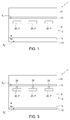
Figures 1-4 are schematic cross-sectional views of embodiments of the present switching device; -
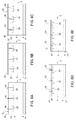
Figures 5A-5E are schematic cross-sectional views of the embodiment illustrated inFigure 1 , during successive steps of a manufacturing process; -
Figures 6A-6E are schematic cross-sectional views of the embodiment illustrated inFigure 2 , during successive steps of a manufacturing process; -
Figures 7A-7E are schematic cross-sectional views of the embodiment illustrated inFigure 3 , during successive steps of a manufacturing process; and -
Figures 8A-8E are schematic cross-sectional views of the embodiment illustrated inFigure 4 , during successive steps of a manufacturing process. -
Figure 1 is a schematic illustration of the structure of a JBS diode, referred to in what follows as thediode 1. - In detail, the
diode 1 comprises asemiconductor body 2, which is made, for example, of a wide bandgap semiconductor, such as for example a material chosen from silicon carbide (SiC), gallium arsenide (GaAs), and gallium nitride (GaN). In what follows, without this implying any loss of generality, it is assumed that thesemiconductor body 2 is of silicon carbide. - The
semiconductor body 2 comprises asubstrate 4 of an N+ type and a firstepitaxial layer 6 of an N type. The firstepitaxial layer 6 is arranged on thesubstrate 4, with which it is in direct contact, and has a doping level lower than the doping level of thesubstrate 4. In addition, thesemiconductor body 2 is delimited at the top and at the bottom by a first surface Sa and a second surface Sb" respectively, which are formed by the firstepitaxial layer 6 and by thesubstrate 4, respectively. - The
diode 1 further comprises abottom contact layer 10, which is made, for example, of nickel silicide and extends underneath the second surface Sb, in direct contact with thesubstrate 4. - The diode further comprises a
conductive layer 12 and atop metallization 14. - The
conductive layer 12 extends over the first surface Sa, in direct contact with the firstepitaxial layer 6, and is of a metal, such as for example a material chosen from nickel, titanium, and molybdenum, or any transition metal. - The
top metallization 14 extends over theconductive layer 12 and in direct contact with the latter. Furthermore, thetop metallization 14 is of a metal material, such as for example aluminium, and has a thickness greater than the thickness of theconductive layer 12. For practical purposes, thetop metallization 14 is designed to contact a conductive element, such as for example a so-called "lead", in order to make it possible to inject current into thediode 1 or draw off current therefrom. Consequently, thetop metallization 14 is designed to withstand the mechanical stresses induced by contact with the conductive element. - The
diode 1 further comprises a plurality of buriedregions 20, of the same semiconductor material as that of thesemiconductor body 2, which are located at a distance from the first surface Sa and thus do not contact theconductive layer 12. - Without this implying any loss of generality, in the embodiment illustrated in
Figure 1 , the buriedregions 20 are of a P type and are substantially the same as one another. Further, the buriedregions 20 extend to approximately the same depth as thesemiconductor body 2. - In greater detail, the buried
regions 20 are separated from one another. In addition, in top plan view, the buriedregions 20 may for example have an elongated shape (for instance, in a direction parallel to the first surface Sa), or else, once again by way of example, a shape chosen from between circular and polygonal. In general, in top plan view, the buriedregions 20 may thus define a strip-like or else cell-like arrangement. - In even greater detail, the
conductive layer 12 and the firstepitaxial layer 6 are such that a so-called Schottky contact is formed between them. In the contact regions between the buriedregions 20 and the firstepitaxial layer 6 there PN junctions are, instead, formed. In other words, the firstepitaxial layer 6 and the buriedregions 20 form, respectively, cathode regions and anode regions of bipolar diodes, while the firstconductive layer 12 and the firstepitaxial layer 6 form, respectively, an anode region and a cathode region of a Schottky diode. In use, the Schottky contact is activated for low biasing voltages of thediode 1, whereas the PN contacts are activated at higher voltages. Furthermore, since the buriedregions 20 are separate from theconductive layer 12, the Schottky contact develops over a particularly extensive area. - As illustrated in
Figure 2 , further possible are embodiments in which thesemiconductor body 2 comprises a secondepitaxial layer 24, arranged on the firstepitaxial layer 6. - For instance, the second
epitaxial layer 24 may have approximately the same doping level as the firstepitaxial layer 6. In the case where, instead, the first and secondepitaxial layers epitaxial layer 24 forms the aforementioned first surface Sa and a third surface Sc. In particular, the secondepitaxial layer 24 overlies, in direct contact, the buriedregions 20, which extend into the firstepitaxial layer 6 starting from the third surface Sc. In practice, the third surface Sc delimits the firstepitaxial layer 6 at the top. -
Figure 3 shows an additional embodiment, in which thediode 1 further comprises a plurality ofregions 28, referred to in what follows as theconnection regions 28. - In detail, the
connection regions 28 are of a conductive material, such as for example nickel silicide, titanium silicide, molybdenum silicide, or a silicide of a transition metal. Furthermore, eachconnection region 28 extends into the firstepitaxial layer 6 starting from the first surface Sa until it contacts a corresponding buriedregion 20. In addition, as illustrated precisely inFigure 3 , eachconnection region 28 may extend at least partially into the corresponding buriedregion 20, and in particular into a top portion of this buriedregion 20. - In greater detail, the
connection regions 28 and the buriedregions 20 are such that the area of contact between eachconnection region 28 and the corresponding buriedregion 20 forms a corresponding ohmic contact. In this way, thediode 1 is characterised by a particular strength in forward biasing. - As illustrated in
Figure 4 , further possible are embodiments whereby thediode 1 includes both theconnection regions 28 and the secondepitaxial layer 24. In this case, theconnection regions 28 extend through the secondepitaxial layer 24. In particular, without this implying any loss of generality, eachtop region 28 comprises a top portion, which extends from the first surface Sa through the secondepitaxial layer 24, and a bottom portion, which extends into the corresponding buriedregion 20. - The
diode 1 illustrated inFigure 1 can be obtained, for example, as shown inFigures 5A-5E and described in detail hereinafter. - Initially, as illustrated
Figure 5A , thesemiconductor body 2, formed by thesubstrate 4 and by the firstepitaxial layer 6, is provided. - Next, as shown in
Figure 5B , formed on the first surface Sa is ahard mask 32, which defines a plurality ofwindows 34. In addition, using thewindows 34, an implantation of a P type is carried out, represented schematically byarrows 36, for example of aluminium ions. The implantation is carried out at high energy (for example, higher than 200 keV) and with a dose ranging for example between 1·1013 and 2·1015 atoms/cm2. Further, this implantation leads to formation ofregions 40 of a buried type, i.e., far from the first surface Sa. Theseregions 40, referred to in what follows as thepreliminary regions 40, are to form the buriedregions 20. - Next, as shown in
Figure 5C , thehard mask 32 is removed. Furthermore, a thermal process of activation of the implanted ions is carried out. This process is carried out at a temperature higher than 1500°C. Following upon the thermal-activation process, eachpreliminary region 40 forms a corresponding buriedregion 20. - Next, as shown in
Figure 5D , deposited on the first surface Sa is amasking layer 42, made, for example, of TEOS oxide. Further, thebottom contact layer 10 is formed underneath the second surface Sb and in direct contact therewith, in a per se known manner and consequently not illustrated. For instance, a bottom layer of metal material (for example, nickel) is formed underneath the second surface Sb and in direct contact therewith, and then a thermal process is carried out, which causes a silicidation of the aforementioned bottom layer of metal material, with consequent formation of thebottom contact layer 10. - Next, as shown in
Figure 5E , themasking layer 42 is removed. In addition, theconductive layer 12 is formed on the first surface Sa, for example by sputtering or evaporation. - Finally, in a way not illustrated, the
top metallization 14 is formed on theconductive layer 12, for example by sputtering or evaporation. - As regards the embodiment illustrated in
Figure 2 , it can be obtained, for example, in the way described hereinafter. - After the operations illustrated in
Figure 5A have been carried out, thehard mask 32 is formed, and an implantation of a P type, represented schematically byarrows 46, is carried out, as shown inFigure 6A . The implantation is carried out at low energy (for instance, less than 200 keV), for example with aluminium ions, and with a dose ranging, for example, between 1·1013 and 2·1015 atoms/cm2. Furthermore, this implantation leads to formation of thepreliminary regions 40, which give out onto the top surface of thefirst epitaxial layer 6. - Next, as shown in
Figure 6B , thehard mask 32 is removed, and then a process of epitaxial growth is carried out for forming thesecond epitaxial layer 24. - Next, as shown in
Figure 6C , a thermal process of activation of the implanted ions is carried out. This process is carried out at a temperature higher than 1500°C. Following upon the thermal-activation process, eachpreliminary region 40 forms a corresponding buriedregion 20. - Next, as shown in
Figure 6D , on thesecond epitaxial layer 24, and thus in contact with the first surface Sa of thesemiconductor body 2, themasking layer 42 is deposited. Furthermore, thebottom contact layer 10 is formed underneath the second surface Sb and in direct contact therewith, for example in the way described previously. - Next, as shown in
Figure 6E , themasking layer 42 is removed. Furthermore, theconductive layer 12 is formed on thesecond epitaxial layer 24, for example by sputtering or evaporation. Next, as described previously, thetop metallization 14 is formed. - As regards the embodiment shown in
Figure 3 , it can be obtained in the way described hereinafter. - Initially the operations illustrated in
Figures 5A-5D are carried out. - Next, as shown in
Figure 7A , a plurality oftrenches 50 is formed, for example by a dry anisotropic etch. In particular, thetrenches 50 are formed by a digging operation that entails selective removal of portions of themasking layer 42 and of thefirst epitaxial layer 6. - In greater detail, each
trench 50 extends from the top surface (designated by Sd) of themasking layer 42 and traverses, beyond themasking layer 42, a corresponding portion of thefirst epitaxial layer 6, arranged between the maskinglayer 42 and a corresponding buriedregion 20, until it extends in part into said corresponding buriedregion 20. In particular, a bottom portion of eachtrench 50 extends through a top portion of the corresponding buriedregion 20. Consequently the bottom of eachtrench 50 extends into the corresponding buriedregion 20. - Next, as shown in
Figure 7B , formed on themasking layer 42 and within thetrenches 50 is alayer 54 of metal material (for example, nickel, titanium or molybdenum), referred to in what follows as thefilling layer 54. The fillinglayer 54 is obtained, for example, by sputtering or evaporation and fills thetrenches 50 completely. - Next, as shown in
Figure 7C , a thermal process is carried out at a temperature comprised between 600°C and 1100°C, and for a duration comprised between 10 and 300 minutes, during which the portions of thefilling layer 54 arranged in contact with the semiconductor material undergo a silicidation process, at the end of which they form correspondingconnection regions 28. The portion of fillinglayer 54 that does not undergo any reaction is instead designated by 55 inFigure 7C . - As shown in
Figure 7D , thenon-reacted portion 55 of thefilling layer 54 is then removed. - Next, as shown in
Figure 7E , themasking layer 42 is removed; further, theconductive layer 12 is formed on thefirst epitaxial layer 6. Next, in a way not illustrated, thetop metallization 14 is formed. - As regards the embodiment illustrated in
Figure 4 , it can be obtained, for example, in the way described hereinafter. - Initially, the operations illustrated in
Figures 6A-6D are carried out. - Next, as shown in
Figure 8A , thetrenches 50 are formed, for example once again by a dry anisotropic etch. In particular, thetrenches 50 are formed by a digging operation that involves selective removal of portions of themasking layer 42 and of thesecond epitaxial layer 24. - In greater detail, each
trench 50 extends from the top surface (designated by Sd) of themasking layer 42 and traverses, beyond themasking layer 42, a corresponding portion of thesecond epitaxial layer 24, arranged between the maskinglayer 42 and a corresponding buriedregion 20, until it extends in part into said corresponding buriedregion 20. In particular, a bottom portion of eachtrench 50 extends through a top portion of the corresponding buriedregion 20. Consequently the bottom of eachtrench 50 extends into the corresponding buriedregion 20. - Next, as shown in
Figure 8B , the fillinglayer 54 is formed on themasking layer 42 and within thetrenches 50. - Next, as shown in
Figure 8C , a thermal process is carried out at a temperature comprised between 600°C and 1100°C, and for a duration comprised between 10 and 300 minutes, during which the portions of thefilling layer 54 arranged in contact with the semiconductor material undergo a silicidation process, at the end of which they form correspondingconnection regions 28. The portion of fillinglayer 54 that does not undergo any reaction is instead designated by 55 inFigure 8C . - As shown in
Figure 8D , thenon-reacted portion 55 of thefilling layer 54 is subsequently removed. - Next, as shown in
Figure 8E , themasking layer 42 is removed. Further, theconductive layer 12 is formed on thesecond epitaxial layer 24. Next, in a way not illustrated, thetop metallization 14 is formed. - The switching device described presents numerous advantages. In particular, it can be shown that the present switching device presents substantially the same electrical field as a so-called JBS trench diode; i.e., it has a value of electrical field lower than the one set up in planar JBS structures, but has a wider Schottky-contact area and thus has a wider useful area for passage of current. Furthermore, the present switching device is characterised by lower leakage currents, as well as by a forward-biasing voltage drop lower than what occurs, for example, in planar JBS structures.
- Finally, it is clear that modifications and variations can be made to the device and to the manufacturing method described and illustrated herein, without thereby departing from the scope of the present invention, as defined in the annexed claims.
- For instance, the types of doping may be reversed with respect to what has been described herein.
- As regards the manufacturing process, the order of the steps may be different from what has been described herein. In addition, the manufacturing process may include further steps other than the ones described. For instance, the manufacturing process may include, in a per se known manner, a so-called step of definition of the active area, which envisages formation of field-oxide regions (not illustrated) delimiting the area in which the JBS diode is to be obtained.
Claims (16)
- A switching device comprising:- a body (2) of semiconductor material, which has a first conductivity type and is delimited by a front surface (Sa);- a contact layer (12) of a first conductive material, which extends in contact with the front surface; and- a plurality of buried regions (20), which have a second conductivity type and are arranged within the semiconductor body, at a distance from the contact layer.
- The switching device according to claim 1, further comprising a plurality of connection regions (28) of a second conductive material, which is different from the first conductive material, each connection region extending in the semiconductor body (2) starting from the front surface (Sa), until it contacts a corresponding buried region (20).
- The switching device according to claim 2, wherein each connection region (28) extends at least in part into the corresponding buried region (20).
- The switching device according to claim 2 or claim 3, wherein the semiconductor body (2) and the contact layer (12) form a Schottky contact; and wherein each connection region (28) forms an ohmic contact with the corresponding buried region (20).
- The switching device according to claim 4, wherein said second material is a silicide of a transition metal.
- The switching device according to any one of the preceding claims, wherein said first material is a transition metal.
- The switching device according to any one of the preceding claims, wherein the body (2) is of silicon carbide.
- The switching device according to any one of the preceding claims, wherein the first conductivity is of an N type and the second conductivity is of a P type.
- The switching device according to any one of the preceding claims, further comprising a top layer (14) of conductive material, which overlies, in direct contact, the contact layer (12) and has a greater thickness than the contact layer.
- A switching device according to any one of the preceding claims, which forms a Junction-barrier Schottky diode (1).
- A process for manufacturing a switching device, comprising the steps of:- forming, within a body (2) of semiconductor material having a first conductivity type and delimited by a front surface (Sa), a plurality of buried regions (20) of a second type of conductivity, said buried regions being arranged at a distance from the front surface; and- forming, in contact with the front surface, a contact layer (12) of a first conductive material.
- The manufacturing process according to claim 11, further comprising the step of forming a plurality of connection regions (28) of a second conductive material, which is different from the first conductive material, so that each connection region will extend in the semiconductor body (2) starting from the front surface (Sa) until it contacts a corresponding buried region (20).
- The manufacturing process according to claim 12, wherein said step of forming a plurality of connection regions (28) is carried out so that each connection region extends at least in part within the corresponding buried region (20).
- The manufacturing process according to any one of claims 11 to 13, wherein said step of forming a plurality of buried regions (20) comprises:- carrying out an ion implantation for forming in the semiconductor body (2) a plurality of preliminary regions (40) of a buried type; and then- carrying out a thermal process of activation of the ions implanted in the preliminary regions.
- The manufacturing process according to any one of claims 11 to 13, wherein said step of forming a plurality of buried regions (20) comprises:- carrying out an ion implantation for forming in the semiconductor body (2) a plurality of preliminary regions (40), which give out onto a temporary surface (Sc) that temporarily delimits said semiconductor body (2); and then- growing an epitaxial layer on said temporary surface;said process further comprising the step of carrying out a thermal process of activation of the ions implanted in the preliminary regions.
- The manufacturing process according to claim 14 or claim 15, when depending upon claim 12 or claim 13, further comprising the steps of:- forming a masking layer (42) of dielectric material on top of said front surface (Sa);- forming a plurality of trenches (50) so that each trench traverses the masking layer, a portion of the semiconductor body (2), and at least part of a corresponding buried region (20);- filling the trenches with a filling region (54) of a third conductive material;- getting portions of the filling region to react thermally with the semiconductor material of the semiconductor body (2) to form a silicide; and then- removing portions (55) of the filling region that have not reacted.
Applications Claiming Priority (1)
| Application Number | Priority Date | Filing Date | Title |
|---|---|---|---|
| ITUB2015A003251A ITUB20153251A1 (en) | 2015-08-27 | 2015-08-27 | SEMICONDUCTOR SWITCHING DEVICE WITH A WIDE BAND FORBIDDEN WITH WIDE SCHOTTKY JUNCTION AREA AND ITS MANUFACTURING PROCESS |
Publications (1)
| Publication Number | Publication Date |
|---|---|
| EP3136447A1 true EP3136447A1 (en) | 2017-03-01 |
Family
ID=54477192
Family Applications (1)
| Application Number | Title | Priority Date | Filing Date |
|---|---|---|---|
| EP16162000.0A Ceased EP3136447A1 (en) | 2015-08-27 | 2016-03-23 | Wide bandgap semiconductor switching device and manufacturing process thereof |
Country Status (4)
| Country | Link |
|---|---|
| US (4) | US9748411B2 (en) |
| EP (1) | EP3136447A1 (en) |
| CN (2) | CN205645825U (en) |
| IT (1) | ITUB20153251A1 (en) |
Families Citing this family (4)
| Publication number | Priority date | Publication date | Assignee | Title |
|---|---|---|---|---|
| US11990553B2 (en) * | 2022-03-31 | 2024-05-21 | Leap Semiconductor Corp. | Merged PiN Schottky (MPS) diode and method of manufacturing the same |
| US20240355938A1 (en) * | 2023-04-20 | 2024-10-24 | Ii-Vi Delaware, Inc. | Buried Grid Double Junction Barrier Schottky Diode and Method of Making |
| CN116344628B (en) * | 2023-05-26 | 2023-08-08 | 湖南楚微半导体科技有限公司 | Schottky diode with shielding gate structure and preparation method thereof |
| CN118800812B (en) * | 2024-09-11 | 2025-03-04 | 珠海格力电子元器件有限公司 | Diode structure and preparation method thereof |
Citations (6)
| Publication number | Priority date | Publication date | Assignee | Title |
|---|---|---|---|---|
| JP2000101101A (en) * | 1998-09-21 | 2000-04-07 | Hitachi Ltd | SiC Schottky diode |
| US6562706B1 (en) * | 2001-12-03 | 2003-05-13 | Industrial Technology Research Institute | Structure and manufacturing method of SiC dual metal trench Schottky diode |
| US20070023781A1 (en) * | 2005-07-28 | 2007-02-01 | Kabushiki Kaisha Toshiba | Semiconductor rectifier |
| US20140061671A1 (en) * | 2012-09-06 | 2014-03-06 | Sumitomo Electric Industries, Ltd. | Wide gap semiconductor device and method for manufacturing same |
| US20140332882A1 (en) * | 2013-05-13 | 2014-11-13 | Sik K. Lui | Trench junction barrier controlled schottky |
| US20150069411A1 (en) * | 2013-09-11 | 2015-03-12 | Infineon Technologies Ag | Semiconductor device, junction field effect transistor and vertical field effect transistor |
Family Cites Families (9)
| Publication number | Priority date | Publication date | Assignee | Title |
|---|---|---|---|---|
| US5949112A (en) * | 1998-05-28 | 1999-09-07 | Lucent Technologies Inc. | Integrated circuits with tub-ties |
| US6404033B1 (en) * | 1999-04-01 | 2002-06-11 | Apd Semiconductor, Inc. | Schottky diode having increased active surface area with improved reverse bias characteristics and method of fabrication |
| US6784486B2 (en) * | 2000-06-23 | 2004-08-31 | Silicon Semiconductor Corporation | Vertical power devices having retrograded-doped transition regions therein |
| US7064408B2 (en) * | 2003-12-10 | 2006-06-20 | Shye-Lin Wu | Schottky barrier diode and method of making the same |
| TWI455209B (en) * | 2009-10-12 | 2014-10-01 | 節能元件股份有限公司 | Ditch-type gold-oxygen semi-P-N junction Xiaoji diode structure and manufacturing method thereof |
| JP2013030618A (en) * | 2011-07-28 | 2013-02-07 | Rohm Co Ltd | Semiconductor device |
| TWI469341B (en) * | 2012-12-20 | 2015-01-11 | Ind Tech Res Inst | Tantalum carbide trench type Schottky barrier element |
| US9425153B2 (en) * | 2013-04-04 | 2016-08-23 | Monolith Semiconductor Inc. | Semiconductor devices comprising getter layers and methods of making and using the same |
| CN204966510U (en) | 2014-06-20 | 2016-01-13 | 意法半导体股份有限公司 | Wide Bandgap High Density Semiconductor Switching Devices |
-
2015
- 2015-08-27 IT ITUB2015A003251A patent/ITUB20153251A1/en unknown
-
2016
- 2016-02-25 CN CN201620144222.5U patent/CN205645825U/en not_active Expired - Lifetime
- 2016-02-25 CN CN201610105439.XA patent/CN106486552A/en active Pending
- 2016-03-03 US US15/059,779 patent/US9748411B2/en active Active
- 2016-03-23 EP EP16162000.0A patent/EP3136447A1/en not_active Ceased
-
2017
- 2017-08-08 US US15/671,615 patent/US10276729B2/en active Active
-
2019
- 2019-03-18 US US16/357,186 patent/US10651319B2/en active Active
-
2020
- 2020-04-06 US US16/841,536 patent/US11177394B2/en active Active
Patent Citations (6)
| Publication number | Priority date | Publication date | Assignee | Title |
|---|---|---|---|---|
| JP2000101101A (en) * | 1998-09-21 | 2000-04-07 | Hitachi Ltd | SiC Schottky diode |
| US6562706B1 (en) * | 2001-12-03 | 2003-05-13 | Industrial Technology Research Institute | Structure and manufacturing method of SiC dual metal trench Schottky diode |
| US20070023781A1 (en) * | 2005-07-28 | 2007-02-01 | Kabushiki Kaisha Toshiba | Semiconductor rectifier |
| US20140061671A1 (en) * | 2012-09-06 | 2014-03-06 | Sumitomo Electric Industries, Ltd. | Wide gap semiconductor device and method for manufacturing same |
| US20140332882A1 (en) * | 2013-05-13 | 2014-11-13 | Sik K. Lui | Trench junction barrier controlled schottky |
| US20150069411A1 (en) * | 2013-09-11 | 2015-03-12 | Infineon Technologies Ag | Semiconductor device, junction field effect transistor and vertical field effect transistor |
Also Published As
| Publication number | Publication date |
|---|---|
| US9748411B2 (en) | 2017-08-29 |
| US20170062626A1 (en) | 2017-03-02 |
| US10651319B2 (en) | 2020-05-12 |
| US10276729B2 (en) | 2019-04-30 |
| US11177394B2 (en) | 2021-11-16 |
| CN205645825U (en) | 2016-10-12 |
| US20170358690A1 (en) | 2017-12-14 |
| US20190214509A1 (en) | 2019-07-11 |
| US20200235248A1 (en) | 2020-07-23 |
| ITUB20153251A1 (en) | 2017-02-27 |
| CN106486552A (en) | 2017-03-08 |
Similar Documents
| Publication | Publication Date | Title |
|---|---|---|
| US11177394B2 (en) | Wide bandgap semiconductor switching device with wide area schottky junction, and manufacturing process thereof | |
| US8497563B2 (en) | Semiconductor device and method for its manufacture | |
| US9711599B2 (en) | Wide bandgap high-density semiconductor switching device and manufacturing process thereof | |
| KR101774124B1 (en) | Semiconductor devices and method for fabricating the same | |
| US20240162040A1 (en) | Manufacturing method of a semiconductor device with efficient edge structure | |
| WO2014085159A1 (en) | Schottky diodes and method of manufacturing the same | |
| TWI446550B (en) | Semiconductor device and method of manufacturing same | |
| US11949025B2 (en) | Wide band gap semiconductor electronic device having a junction-barrier Schottky diode | |
| CN102473738A (en) | Semiconductor device | |
| US8183660B2 (en) | Semiconductor component having rectifying junctions of different magnitudes and method for producing the same | |
| US20240113235A1 (en) | Silicon carbide device with single metallization process for ohmic and schottky contacts | |
| JP6004109B2 (en) | Semiconductor device and manufacturing method thereof | |
| EP2462620B1 (en) | Semiconductor arrangement and method for producing it | |
| CN114220870A (en) | Omnidirectional Schottky contact trench type semiconductor device and manufacturing method thereof | |
| US12272747B2 (en) | Electronic device including a transistor structure | |
| CN116646406A (en) | Wide bandgap semiconductor device and its manufacturing method | |
| JP2010040857A (en) | Semiconductor device | |
| US20050184355A1 (en) | Semiconductor device | |
| US10748780B2 (en) | Manufacturing method of silicon carbide semiconductor device |
Legal Events
| Date | Code | Title | Description |
|---|---|---|---|
| PUAI | Public reference made under article 153(3) epc to a published international application that has entered the european phase |
Free format text: ORIGINAL CODE: 0009012 |
|
| AK | Designated contracting states |
Kind code of ref document: A1 Designated state(s): AL AT BE BG CH CY CZ DE DK EE ES FI FR GB GR HR HU IE IS IT LI LT LU LV MC MK MT NL NO PL PT RO RS SE SI SK SM TR |
|
| AX | Request for extension of the european patent |
Extension state: BA ME |
|
| 17P | Request for examination filed |
Effective date: 20170825 |
|
| RBV | Designated contracting states (corrected) |
Designated state(s): AL AT BE BG CH CY CZ DE DK EE ES FI FR GB GR HR HU IE IS IT LI LT LU LV MC MK MT NL NO PL PT RO RS SE SI SK SM TR |
|
| 17Q | First examination report despatched |
Effective date: 20181017 |
|
| STAA | Information on the status of an ep patent application or granted ep patent |
Free format text: STATUS: THE APPLICATION HAS BEEN REFUSED |
|
| 18R | Application refused |
Effective date: 20200303 |