EP3136395A1 - Circuit and method for biasing non-volatile memory cells - Google Patents
Circuit and method for biasing non-volatile memory cells Download PDFInfo
- Publication number
- EP3136395A1 EP3136395A1 EP16162017.4A EP16162017A EP3136395A1 EP 3136395 A1 EP3136395 A1 EP 3136395A1 EP 16162017 A EP16162017 A EP 16162017A EP 3136395 A1 EP3136395 A1 EP 3136395A1
- Authority
- EP
- European Patent Office
- Prior art keywords
- bias
- current
- node
- compensation
- coupled
- Prior art date
- Legal status (The legal status is an assumption and is not a legal conclusion. Google has not performed a legal analysis and makes no representation as to the accuracy of the status listed.)
- Granted
Links
Images


Classifications
-
- G—PHYSICS
- G11—INFORMATION STORAGE
- G11C—STATIC STORES
- G11C16/00—Erasable programmable read-only memories
- G11C16/02—Erasable programmable read-only memories electrically programmable
- G11C16/06—Auxiliary circuits, e.g. for writing into memory
- G11C16/26—Sensing or reading circuits; Data output circuits
- G11C16/28—Sensing or reading circuits; Data output circuits using differential sensing or reference cells, e.g. dummy cells
-
- G—PHYSICS
- G05—CONTROLLING; REGULATING
- G05F—SYSTEMS FOR REGULATING ELECTRIC OR MAGNETIC VARIABLES
- G05F3/00—Non-retroactive systems for regulating electric variables by using an uncontrolled element, or an uncontrolled combination of elements, such element or such combination having self-regulating properties
- G05F3/02—Regulating voltage or current
- G05F3/08—Regulating voltage or current wherein the variable is DC
- G05F3/10—Regulating voltage or current wherein the variable is DC using uncontrolled devices with non-linear characteristics
- G05F3/16—Regulating voltage or current wherein the variable is DC using uncontrolled devices with non-linear characteristics being semiconductor devices
- G05F3/20—Regulating voltage or current wherein the variable is DC using uncontrolled devices with non-linear characteristics being semiconductor devices using diode- transistor combinations
- G05F3/24—Regulating voltage or current wherein the variable is DC using uncontrolled devices with non-linear characteristics being semiconductor devices using diode- transistor combinations wherein the transistors are of the field-effect type only
- G05F3/242—Regulating voltage or current wherein the variable is DC using uncontrolled devices with non-linear characteristics being semiconductor devices using diode- transistor combinations wherein the transistors are of the field-effect type only with compensation for device parameters, e.g. channel width modulation, threshold voltage, processing, or external variations, e.g. temperature, loading, supply voltage
- G05F3/245—Regulating voltage or current wherein the variable is DC using uncontrolled devices with non-linear characteristics being semiconductor devices using diode- transistor combinations wherein the transistors are of the field-effect type only with compensation for device parameters, e.g. channel width modulation, threshold voltage, processing, or external variations, e.g. temperature, loading, supply voltage producing a voltage or current as a predetermined function of the temperature
-
- G—PHYSICS
- G11—INFORMATION STORAGE
- G11C—STATIC STORES
- G11C16/00—Erasable programmable read-only memories
- G11C16/02—Erasable programmable read-only memories electrically programmable
- G11C16/06—Auxiliary circuits, e.g. for writing into memory
- G11C16/10—Programming or data input circuits
- G11C16/14—Circuits for erasing electrically, e.g. erase voltage switching circuits
-
- G—PHYSICS
- G11—INFORMATION STORAGE
- G11C—STATIC STORES
- G11C16/00—Erasable programmable read-only memories
- G11C16/02—Erasable programmable read-only memories electrically programmable
- G11C16/06—Auxiliary circuits, e.g. for writing into memory
- G11C16/24—Bit-line control circuits
-
- G—PHYSICS
- G11—INFORMATION STORAGE
- G11C—STATIC STORES
- G11C16/00—Erasable programmable read-only memories
- G11C16/02—Erasable programmable read-only memories electrically programmable
- G11C16/06—Auxiliary circuits, e.g. for writing into memory
- G11C16/30—Power supply circuits
-
- G—PHYSICS
- G11—INFORMATION STORAGE
- G11C—STATIC STORES
- G11C5/00—Details of stores covered by group G11C11/00
- G11C5/14—Power supply arrangements, e.g. power down, chip selection or deselection, layout of wirings or power grids, or multiple supply levels
- G11C5/147—Voltage reference generators, voltage or current regulators; Internally lowered supply levels; Compensation for voltage drops
-
- G—PHYSICS
- G11—INFORMATION STORAGE
- G11C—STATIC STORES
- G11C7/00—Arrangements for writing information into, or reading information out from, a digital store
- G11C7/12—Bit line control circuits, e.g. drivers, boosters, pull-up circuits, pull-down circuits, precharging circuits, equalising circuits, for bit lines
-
- G—PHYSICS
- G11—INFORMATION STORAGE
- G11C—STATIC STORES
- G11C7/00—Arrangements for writing information into, or reading information out from, a digital store
- G11C7/14—Dummy cell management; Sense reference voltage generators
-
- G—PHYSICS
- G11—INFORMATION STORAGE
- G11C—STATIC STORES
- G11C16/00—Erasable programmable read-only memories
- G11C16/02—Erasable programmable read-only memories electrically programmable
- G11C16/06—Auxiliary circuits, e.g. for writing into memory
- G11C16/08—Address circuits; Decoders; Word-line control circuits
-
- G—PHYSICS
- G11—INFORMATION STORAGE
- G11C—STATIC STORES
- G11C16/00—Erasable programmable read-only memories
- G11C16/02—Erasable programmable read-only memories electrically programmable
- G11C16/06—Auxiliary circuits, e.g. for writing into memory
- G11C16/10—Programming or data input circuits
-
- G—PHYSICS
- G11—INFORMATION STORAGE
- G11C—STATIC STORES
- G11C7/00—Arrangements for writing information into, or reading information out from, a digital store
- G11C7/04—Arrangements for writing information into, or reading information out from, a digital store with means for avoiding disturbances due to temperature effects
-
- G—PHYSICS
- G11—INFORMATION STORAGE
- G11C—STATIC STORES
- G11C8/00—Arrangements for selecting an address in a digital store
- G11C8/10—Decoders
Definitions
- the present invention relates to a circuit and a method for biasing non-volatile memory cells.
- bias circuits have some limitations, which at times do not enable satisfactory performance to be achieved as regards the biasing quantities.
- the drain voltage also depends upon the current that flows through the cells during the program step (in general, this current initially has a high value that decreases as the threshold of the cells selected for programming increases).
- a reference current independent of temperature simulates the cell current in the program step.
- Other current contributions which are, instead, not immune to temperature variations and are significantly affected by process spread may, however, add to the reference current.
- the non-stable current contributions do not allow to copy the conditions present in the memory array with sufficient accuracy. Biasing may thus prove inadequate.
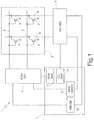
- a non-volatile memory device for example of a flash type, is designated as a whole by the reference number 1.
- the device 1 comprises a memory array 2, formed by a plurality of memory cells 3 arranged in rows and columns, a column decoder 5, a row decoder 6, and a program and read circuit 7.
- memory cells 3 arranged along a same column are connected to a same bitline 8 and memory cells 3 arranged along a same row are connected by a same wordline 9.
- the column decoder 5 and row decoder 6, both of a known type, are configured to connect selectively a bitline 8 (or a set of bitlines 8) and a wordline 9, respectively, which are addressed for program and read operations by the program and read circuit 7.
- the program and read circuit 7 comprises a column bias circuit 10, a row bias circuit 11, a program circuit 12, and a read/verify circuit 13.
- the column bias circuit 10 and the row bias circuit 11 are coupled, respectively, to the bitlines 8 and the wordlines 9 each time selected through the column decoder 5 and the row decoder 6.
- the bias circuit 10 which is illustrated in greater detail in Figure 2 , comprises a reference current generator 15, a bias resistive divider 16, a voltage regulator 17, a dummy decoding path 18, and a compensation stage 20.
- Figure 2 further shows a memory cell 3 selected and connected to the bias circuit 10 through a respective bitline 8 and the column decoder 5.
- the reference current generator 15 has a terminal coupled to one current adder node 21 and one terminal coupled to a ground line 22.
- the reference current generator 15 is programmable and supplies a reference current I T that reproduces the average current flowing in the memory cell 3 during programming.
- the reference current I T may be decremented in steps, for example of 15 ⁇ A.
- the bias resistive divider 16 comprises a plurality of resistive modules 24 between a cell bias node 25 and the ground line 22.
- the resistive modules 24 are the same as one another.
- a first set of resistive modules 24 (just one module 24 in the example of Figure 2 ) is connected between a bias regulation node 27 and the ground line 22 and defines a first portion 16.1 of the divider 16
- a second set of resistive modules 24 is connected between the cell bias node 25 and the bias regulation node 27 and defines a second portion 16.2 of the divider 16.
- the voltage regulator 17 is configured to impose a reference voltage V R on the bias regulation node 27.
- the voltage regulator 17 comprises an operational amplifier 28, a reference voltage generator 29, and a limiting transistor 30.
- the operational amplifier 28 has an input terminal, for example a inverting terminal, coupled to the bias regulation node 27, an input terminal, for example a non-inverting terminal, coupled to the reference voltage generator 29 for receiving the reference voltage V R , and an output coupled to a control terminal of the limiting transistor 30.
- the reference voltage generator 29 is configured so that the reference voltage V R is independent of the temperature.
- the reference voltage generator 29 is a band-gap generator.
- the limiting transistor 30 has conduction terminals, one of which is connected to a boosted line 32, which receives a boosted voltage V PP from a voltage booster stage (not illustrated), and the other to a global bias line 33.
- the limiting transistor 30 operates on the bias regulation node 27 through the dummy decoding path 18 and the second portion 16.2 of the divider 16.
- a bias current I B flows through the bias resistive divider 16 and is given by the ratio between the reference voltage V R and the resistance of the first portion 16.1 of the bias resistive divider 16 (in this case, of a resistive module 24).
- the cell bias node 25 is set to a cell bias voltage V BDC , determined by the overall resistance of the bias resistive divider 16 and by the bias current I B imposed by the voltage regulator 17.
- the cell bias voltage V BDC is KV R .
- the dummy decoding path 18 is connected between the global bias line 33 and the cell bias node 25 and replicates the conductive path presented by the column decoder 5.
- the dummy decoding path 18 comprises a dummy enable transistor 35, which replicates an enable transistor 36 of the column decoder 5, and a series of dummy decoding transistors 37, that are equal in number to, and the same in structure as, the decoding transistors 38 of the column decoder 5.
- the dummy decoding transistors 37 are kept in conduction by a dummy decoding signal YD during the program and erase operations. Passage of current through the dummy decoding path 18 causes a voltage drop and sets the global bias line 33 to a line bias voltage V BDL.
- the cell bias node 25 and the current adder node 21 are selectively connectable through an enable transistor 40.
- the global bias line 33 and the cell bias node 25 are selectively connectable through an enable transistor 41, which is controlled in a complementary way with respect to the enable transistor 40.
- the enable transistor 40 and the enable transistor 41 are both of an NMOS type; the former receives, however, a direct enable signal EN, whereas the latter receives a negated enable signal ENN.
- the dummy enable transistor 35 and the enable transistor 40 are, instead, driven to be both in conduction or both in cut-off.
- the dummy transistor 35 is of a PMOS type and receives the negated enable signal ENN.
- the compensation stage 20 is configured to inject into the current adder node 21 a compensation current I C equal, and of opposite sign with respect, to the bias current I B that flows through the bias resistive divider 16.
- the compensation stage 20 comprises a resistive element 43, a voltage regulator 45, a current mirror 46, and an enable transistor 47.
- the resistive element 43 is connected between a compensation regulation node 48 and the ground line 22 and has the same impedance as the first portion 16.1 of the divider 16.
- the voltage regulator 45 is configured to impose the reference voltage V R on the compensation regulation node 48 and comprises an operational amplifier 50, a reference voltage generator 51, and a limiting transistor 52.
- the operational amplifier 50 has an input terminal, for example an inverting one, coupled to the compensation regulation node 48, an input terminal, for example a non-inverting one, coupled to the reference voltage generator 51, and an output coupled to a control terminal of the limiting transistor 52.
- the reference voltage generator 51 supplies the same reference voltage V R as that supplied by the reference voltage generator 29 and also this is independent of the temperature; for example, it is of a band-gap type.
- the conduction terminals of the limiting transistor 52 are connected one to the compensation regulation node 48 and the other to a reference branch 46a of the current mirror 46.
- the voltage regulator 45 imposes on the compensation regulation node 48 the same reference voltage V R as the one that is present on the bias regulation node 27 and the impedance of the resistive element 43 is equal to the impedance of the first portion 16.1 of the divider 16, the compensation current I C that flows through the limiting transistor 52 and the resistive element 43 is equal in absolute value to the bias current I B .
- An output branch 46b of the current mirror 46 which is for example in cascode configuration, replicates the compensation current I C , which is injected into the current adder node 21 through the enable transistor 47.
- the enable transistor 47 is identical to the enable transistor 40 and is driven by the same direct enable signal EN.
- the bias circuit 10 operates as described in what follows.
- the bias circuit 10 is activated by the direct enable signal EN and the negated enable signal ENN, the enable transistors 35, 40, 47 are in conduction, whereas the enable transistor 41 is cut-off.
- the voltage regulator 17 sets the bias regulation node 27 to the reference voltage V R , thus causing the bias current I B to flow, which brings the cell bias node 25 to the cell bias voltage V BDC .
- the compensation stage 20 supplies the compensation current I C to the current adder node 21.
- the compensation current I C is generated starting from a voltage reference and a resistive element identical to the ones used for generating the bias current I B . The two currents are thus equal.
- the bias current I B would be added to the reference current I T and would affect the potential drop on the dummy decoding path 18, i.e., the potential difference V BDL -V BDC .
- the bias current I B may be affected by temperature variations, in addition to process spread, also the potential difference V BDL -V BDC would be affected by unpredictable elements of variability. It would hence not be possible to reproduce in a stable way the bias conditions of the memory cells 3 selected for programming, in particular as regards the potential difference between the global bias line 33 and the drain terminal of the selected cells 3.
- a bias circuit 110 comprises a reference current generator 115, a bias resistive divider 116, a voltage regulator 117, and a dummy decoding path 118, which are substantially the same as the reference current generator 15, the bias resistive divider 16, and the voltage regulator 17 already described.
- the reference current generator 115 generates a reference current I T ', which is picked up from a current adder node 121.
- the voltage regulator 117 is configured to impose a reference voltage on a bias regulation node 127 of the bias resistive divider 116 to obtain a bias current I B ', and a cell bias voltage V BDC ' on a cell bias node 125 to which the bias resistive divider 116 is coupled.
- the dummy decoding path 118 is connected between a global bias line 133 and the cell bias node 125, which is in turn connected to the current adder node 121 through an enable transistor 140.
- the bias circuit 110 further comprises a compensation stage 120 configured to inject into the current adder node 121 a compensation current I C ' equal to the bias current I B ' that flows through the bias resistive divider 116.
- the compensation stage 120 comprises a sense current mirror 145 and a compensation current mirror 146, which is coupled to the current adder node 121 through an enable transistor 147.
- the sense current mirror 145 has a sense branch 145a, coupled to the bias resistive divider 116 for receiving the bias current I B ', and an output branch 145b. More precisely, the sense branch 145a of the sense current mirror 145 and the bias resistive divider 116 are coupled to a virtual ground node 148. To obtain the function of virtual ground, an operational amplifier 150 has an input coupled to a ground line 151, an input coupled to the virtual ground node 148, and an output coupled to a regulated negative line 152, which is used also as negative reference for the sense current mirror 145.
- the compensation current mirror 146 has a sense branch 146a coupled to the output branch 145a of the sense current mirror 145 and an output branch 146b, which is selectively connectable to the current adder node 121 for supplying the compensation current I C '.
- the compensation current I C ' balances exactly the bias current I B ' absorbed by the bias resistive divider 116. Consequently, the same reference current I T ' that is supplied by the reference current generator 115 also flows through the dummy decoding path 118, the conditions of which are not affected by temperature variations.
- Illustrated in Figure 4 is an electronic system 200, incorporating the non-volatile memory device 1 described with reference to Figures 1 and 2 .
- the electronic system 200 may be an electronic device of any type, in particular portable and supplied autonomously, such as, by way of non-limiting example, a cellphone, a portable computer, a video camera, a photographic camera, a multimedia reader, a portable apparatus for video games, a motion-activated user interface for computers or consoles for video games, a satellite navigation device, or a so-called "wearable" electronic device.
- the electronic system 200 is a cellphone.
- the electronic system 200 may comprise a control unit 201 and the non-volatile memory device 2.
- the electronic system 200 may further comprise a casing 203, rigidly coupled to which is an impact sensor 204, a microphone 205, for example a micro-electromechanical microphone coupled to an acquisition interface of an audio module 206, an RF communication module 207 coupled to an antenna 208, a display 210, a filming device 212, a serial connection port 213, for example a USB port, and a battery 215 for autonomous supply.
- a casing 203 rigidly coupled to which is an impact sensor 204, a microphone 205, for example a micro-electromechanical microphone coupled to an acquisition interface of an audio module 206, an RF communication module 207 coupled to an antenna 208, a display 210, a filming device 212, a serial connection port 213, for example a USB port, and a battery 215 for autonomous supply.
- the non-volatile memory device 2 may contain code portions executable by the control unit 201. Furthermore, the control unit 201 may co-operate with the non-volatile memory device for recording, for example, images acquired through the filming device 212, audio files acquired by the microphone 205 or other files received through the RF communication module 207 or the serial connection port 213.
Landscapes
- Engineering & Computer Science (AREA)
- Power Engineering (AREA)
- Microelectronics & Electronic Packaging (AREA)
- Physics & Mathematics (AREA)
- Nonlinear Science (AREA)
- Electromagnetism (AREA)
- General Physics & Mathematics (AREA)
- Radar, Positioning & Navigation (AREA)
- Automation & Control Theory (AREA)
- Read Only Memory (AREA)
Abstract
Description
- The present invention relates to a circuit and a method for biasing non-volatile memory cells.
- As is known, in program and read operations of non-volatile memory cells a delicate aspect regards proper biasing of the drain terminals of the cells selected. The problem of biasing is generally felt, but regards in particular non-volatile memories of an electrical type, such as flash memories, which are, further, the most widespread. On one hand, in fact, cells that are not properly biased are subjected to stresses, which, over time and with repetition of programm/erase/read cycles, may cause deterioration, especially of the gate-oxide regions. On the other hand, the outcome of the operations may be affected by inadequate biasing of the drain terminals. For program and erase operations the problem of stability of the biasing quantities is evidently more significant since an error during program/erase step causes systematic errors in the read step.
- Known bias circuits have some limitations, which at times do not enable satisfactory performance to be achieved as regards the biasing quantities. For instance, the drain voltage also depends upon the current that flows through the cells during the program step (in general, this current initially has a high value that decreases as the threshold of the cells selected for programming increases). In the program circuits, a reference current independent of temperature simulates the cell current in the program step. Other current contributions, which are, instead, not immune to temperature variations and are significantly affected by process spread may, however, add to the reference current. The non-stable current contributions do not allow to copy the conditions present in the memory array with sufficient accuracy. Biasing may thus prove inadequate.
- It is an object of the present invention to provide a circuit and a method for biasing non-volatile memory cells that will enable the limitations described to be overcome or at least mitigated.
- According to the present invention, a circuit and a method for biasing non-volatile memory cells are provided, as defined in
claims - For a better understanding of the invention, some embodiments thereof will now be described, purely by way of non-limiting example and with reference to the attached drawings, wherein:
-
Figure 1 is a simplified block diagram of a non-volatile memory device; -
Figure 2 is a simplified circuit diagram of a circuit for biasing non-volatile memory cells according to one embodiment of the present invention, incorporated in the non-volatile memory device ofFigure 1 ; -
Figure 3 is a simplified circuit diagram of a circuit for biasing non-volatile memory cells according to a different embodiment of the present invention; and -
Figure 4 is a simplified block diagram of an electronic system incorporating the non-volatile memory device ofFigure 1 . - In
Figure 1 , a non-volatile memory device, for example of a flash type, is designated as a whole by thereference number 1. Thedevice 1 comprises amemory array 2, formed by a plurality ofmemory cells 3 arranged in rows and columns, acolumn decoder 5, a row decoder 6, and a program and readcircuit 7. Thememory cells 3 have N storage levels and are thus able to store a number of bits B equal to log2 N (for example, N = 4, B = 2; with N = 2 and B = 1 conventional two-level cells are obtained). Furthermore,memory cells 3 arranged along a same column are connected to asame bitline 8 andmemory cells 3 arranged along a same row are connected by asame wordline 9. Thecolumn decoder 5 and row decoder 6, both of a known type, are configured to connect selectively a bitline 8 (or a set of bitlines 8) and awordline 9, respectively, which are addressed for program and read operations by the program and readcircuit 7. - The program and read
circuit 7 comprises acolumn bias circuit 10, arow bias circuit 11, aprogram circuit 12, and a read/verify circuit 13. Thecolumn bias circuit 10 and therow bias circuit 11 are coupled, respectively, to thebitlines 8 and thewordlines 9 each time selected through thecolumn decoder 5 and the row decoder 6. - The
bias circuit 10, which is illustrated in greater detail inFigure 2 , comprises areference current generator 15, a biasresistive divider 16, avoltage regulator 17, adummy decoding path 18, and acompensation stage 20.Figure 2 further shows amemory cell 3 selected and connected to thebias circuit 10 through arespective bitline 8 and thecolumn decoder 5. - The
reference current generator 15 has a terminal coupled to onecurrent adder node 21 and one terminal coupled to aground line 22. The referencecurrent generator 15 is programmable and supplies a reference current IT that reproduces the average current flowing in thememory cell 3 during programming. In one embodiment, the reference current IT may be decremented in steps, for example of 15 µA. - The bias
resistive divider 16 comprises a plurality ofresistive modules 24 between acell bias node 25 and theground line 22. In one embodiment, theresistive modules 24 are the same as one another. In detail, a first set of resistive modules 24 (just onemodule 24 in the example ofFigure 2 ) is connected between abias regulation node 27 and theground line 22 and defines a first portion 16.1 of thedivider 16, and a second set ofresistive modules 24 is connected between thecell bias node 25 and thebias regulation node 27 and defines a second portion 16.2 of thedivider 16. - The
voltage regulator 17 is configured to impose a reference voltage VR on thebias regulation node 27. In one embodiment, thevoltage regulator 17 comprises anoperational amplifier 28, areference voltage generator 29, and a limitingtransistor 30. Theoperational amplifier 28 has an input terminal, for example a inverting terminal, coupled to thebias regulation node 27, an input terminal, for example a non-inverting terminal, coupled to thereference voltage generator 29 for receiving the reference voltage VR, and an output coupled to a control terminal of the limitingtransistor 30. Thereference voltage generator 29 is configured so that the reference voltage VR is independent of the temperature. In one embodiment, thereference voltage generator 29 is a band-gap generator. The limitingtransistor 30 has conduction terminals, one of which is connected to a boostedline 32, which receives a boosted voltage VPP from a voltage booster stage (not illustrated), and the other to aglobal bias line 33. The limitingtransistor 30 operates on thebias regulation node 27 through thedummy decoding path 18 and the second portion 16.2 of thedivider 16. - As a result of the action of the
voltage regulator 17, a bias current IB flows through the biasresistive divider 16 and is given by the ratio between the reference voltage VR and the resistance of the first portion 16.1 of the bias resistive divider 16 (in this case, of a resistive module 24). Furthermore, thecell bias node 25 is set to a cell bias voltage VBDC, determined by the overall resistance of the biasresistive divider 16 and by the bias current IB imposed by thevoltage regulator 17. In one embodiment, in which K equal resistive modules are present, the cell bias voltage VBDC is KVR. - The
dummy decoding path 18 is connected between theglobal bias line 33 and thecell bias node 25 and replicates the conductive path presented by thecolumn decoder 5. In particular, thedummy decoding path 18 comprises a dummy enabletransistor 35, which replicates an enabletransistor 36 of thecolumn decoder 5, and a series ofdummy decoding transistors 37, that are equal in number to, and the same in structure as, thedecoding transistors 38 of thecolumn decoder 5. Thedummy decoding transistors 37 are kept in conduction by a dummy decoding signal YD during the program and erase operations. Passage of current through thedummy decoding path 18 causes a voltage drop and sets theglobal bias line 33 to a line bias voltage VBDL. - The
cell bias node 25 and thecurrent adder node 21 are selectively connectable through an enabletransistor 40. Likewise, theglobal bias line 33 and thecell bias node 25 are selectively connectable through an enabletransistor 41, which is controlled in a complementary way with respect to the enabletransistor 40. In one embodiment, the enabletransistor 40 and the enabletransistor 41 are both of an NMOS type; the former receives, however, a direct enable signal EN, whereas the latter receives a negated enable signal ENN. The dummy enabletransistor 35 and the enabletransistor 40 are, instead, driven to be both in conduction or both in cut-off. In one embodiment, in particular, thedummy transistor 35 is of a PMOS type and receives the negated enable signal ENN. - The
compensation stage 20 is configured to inject into the current adder node 21 a compensation current IC equal, and of opposite sign with respect, to the bias current IB that flows through the biasresistive divider 16. - In detail, the
compensation stage 20 comprises aresistive element 43, avoltage regulator 45, acurrent mirror 46, and an enabletransistor 47. - The
resistive element 43 is connected between acompensation regulation node 48 and theground line 22 and has the same impedance as the first portion 16.1 of thedivider 16. - The
voltage regulator 45 is configured to impose the reference voltage VR on thecompensation regulation node 48 and comprises anoperational amplifier 50, areference voltage generator 51, and a limitingtransistor 52. Theoperational amplifier 50 has an input terminal, for example an inverting one, coupled to thecompensation regulation node 48, an input terminal, for example a non-inverting one, coupled to thereference voltage generator 51, and an output coupled to a control terminal of the limitingtransistor 52. Thereference voltage generator 51 supplies the same reference voltage VR as that supplied by thereference voltage generator 29 and also this is independent of the temperature; for example, it is of a band-gap type. The conduction terminals of the limitingtransistor 52 are connected one to thecompensation regulation node 48 and the other to areference branch 46a of thecurrent mirror 46. - Since the
voltage regulator 45 imposes on thecompensation regulation node 48 the same reference voltage VR as the one that is present on thebias regulation node 27 and the impedance of theresistive element 43 is equal to the impedance of the first portion 16.1 of thedivider 16, the compensation current IC that flows through the limitingtransistor 52 and theresistive element 43 is equal in absolute value to the bias current IB. - An
output branch 46b of thecurrent mirror 46, which is for example in cascode configuration, replicates the compensation current IC, which is injected into thecurrent adder node 21 through the enabletransistor 47. The enabletransistor 47 is identical to the enabletransistor 40 and is driven by the same direct enable signal EN. - The
bias circuit 10 operates as described in what follows. When thebias circuit 10 is activated by the direct enable signal EN and the negated enable signal ENN, the enabletransistors transistor 41 is cut-off. Thevoltage regulator 17 sets thebias regulation node 27 to the reference voltage VR, thus causing the bias current IB to flow, which brings thecell bias node 25 to the cell bias voltage VBDC. At the same time, thecompensation stage 20 supplies the compensation current IC to thecurrent adder node 21. As already mentioned, the compensation current IC is generated starting from a voltage reference and a resistive element identical to the ones used for generating the bias current IB. The two currents are thus equal. For this reason, the balance of currents at thenodes dummy decoding path 18 is equal to the reference current IT, which reproduces the average current flowing in thememory cell 3 during programming. In the absence of thecompensation stage 20, instead, the bias current IB would be added to the reference current IT and would affect the potential drop on thedummy decoding path 18, i.e., the potential difference VBDL-VBDC. Given that the bias current IB may be affected by temperature variations, in addition to process spread, also the potential difference VBDL-VBDC would be affected by unpredictable elements of variability. It would hence not be possible to reproduce in a stable way the bias conditions of thememory cells 3 selected for programming, in particular as regards the potential difference between theglobal bias line 33 and the drain terminal of the selectedcells 3. - Use of the
compensation stage 20, instead, allows to eliminate the dependence of the current in thedummy decoding path 18 upon the bias current IB, thus reducing dependence upon the temperature and upon the process spread in the components. -
Figure 3 illustrates a different embodiment of the invention. In this case, a bias circuit 110 comprises a referencecurrent generator 115, a biasresistive divider 116, avoltage regulator 117, and adummy decoding path 118, which are substantially the same as the referencecurrent generator 15, the biasresistive divider 16, and thevoltage regulator 17 already described. In particular, the referencecurrent generator 115 generates a reference current IT', which is picked up from acurrent adder node 121. Thevoltage regulator 117 is configured to impose a reference voltage on abias regulation node 127 of the biasresistive divider 116 to obtain a bias current IB', and a cell bias voltage VBDC' on acell bias node 125 to which the biasresistive divider 116 is coupled. Thedummy decoding path 118 is connected between a global bias line 133 and thecell bias node 125, which is in turn connected to thecurrent adder node 121 through an enabletransistor 140. - The bias circuit 110 further comprises a
compensation stage 120 configured to inject into the current adder node 121 a compensation current IC' equal to the bias current IB' that flows through the biasresistive divider 116. In detail, thecompensation stage 120 comprises a sensecurrent mirror 145 and a compensationcurrent mirror 146, which is coupled to thecurrent adder node 121 through an enabletransistor 147. - The sense
current mirror 145 has asense branch 145a, coupled to the biasresistive divider 116 for receiving the bias current IB', and anoutput branch 145b. More precisely, thesense branch 145a of the sensecurrent mirror 145 and the biasresistive divider 116 are coupled to avirtual ground node 148. To obtain the function of virtual ground, anoperational amplifier 150 has an input coupled to aground line 151, an input coupled to thevirtual ground node 148, and an output coupled to a regulatednegative line 152, which is used also as negative reference for the sensecurrent mirror 145. The compensationcurrent mirror 146 has asense branch 146a coupled to theoutput branch 145a of the sensecurrent mirror 145 and anoutput branch 146b, which is selectively connectable to thecurrent adder node 121 for supplying the compensation current IC'. On the hypothesis, which may readily be verified, that the sensecurrent mirror 145 and the compensationcurrent mirror 146 both have a unit mirror ratio, the compensation current IC' balances exactly the bias current IB' absorbed by the biasresistive divider 116. Consequently, the same reference current IT' that is supplied by the referencecurrent generator 115 also flows through thedummy decoding path 118, the conditions of which are not affected by temperature variations. - Connection of the bias
resistive divider 116 to thevirtual ground node 148 enables the cell bias voltage VBDC' to be rendered substantially independent of the temperature and of the process spread. - Illustrated in
Figure 4 is anelectronic system 200, incorporating thenon-volatile memory device 1 described with reference toFigures 1 and2 . - The
electronic system 200 may be an electronic device of any type, in particular portable and supplied autonomously, such as, by way of non-limiting example, a cellphone, a portable computer, a video camera, a photographic camera, a multimedia reader, a portable apparatus for video games, a motion-activated user interface for computers or consoles for video games, a satellite navigation device, or a so-called "wearable" electronic device. In the embodiment ofFigure 4 , theelectronic system 200 is a cellphone. - The
electronic system 200 may comprise acontrol unit 201 and thenon-volatile memory device 2. - The
electronic system 200 may further comprise acasing 203, rigidly coupled to which is animpact sensor 204, amicrophone 205, for example a micro-electromechanical microphone coupled to an acquisition interface of anaudio module 206, anRF communication module 207 coupled to anantenna 208, adisplay 210, afilming device 212, aserial connection port 213, for example a USB port, and abattery 215 for autonomous supply. - The
non-volatile memory device 2 may contain code portions executable by thecontrol unit 201. Furthermore, thecontrol unit 201 may co-operate with the non-volatile memory device for recording, for example, images acquired through thefilming device 212, audio files acquired by themicrophone 205 or other files received through theRF communication module 207 or theserial connection port 213. - It can be noted that the scope of the present invention is not limited to embodiments necessarily having specifically one of the devices listed or all of them together.
- Finally, it is evident that modifications and variations can be made to the circuit and to the method described herein, without thereby departing from the scope of the present invention, as defined in the annexed claims.
Claims (14)
- A bias circuit for biasing non-volatile memory cells comprising:a dummy decoding path (18; 118) between a global bias line (33; 133) and a bias node (25; 125);a reference current generator (15; 115), coupled to the dummy decoding path (18; 118) and configured to supply a reference current (IT; IT');a bias stage (16, 17; 116, 117) configured to set a cell bias voltage (VBDC; VBDC') on the bias node (25; 125); anda compensation stage (20; 120), configured to compensate a current absorption of the bias stage (16, 17; 116, 117) at the bias node (25; 125) so that the reference current (IT; IT') will flow through the dummy decoding path (18; 118).
- The bias circuit according to claim 1, wherein the bias stage (16, 17; 116; 117) comprises a bias resistive path (16; 116), coupled to the bias node (25; 125), and a bias voltage regulator (17; 117), configured to impose a reference voltage (VR) on a bias regulation node (27; 127) of the bias resistive path (16; 116); and the compensation stage (20) is configured to supply a compensation current (IC) equal, and of opposite sign with respect, to a bias current (IB; IB') flowing in the bias resistive path (16; 116).
- The bias circuit according to claim 2, wherein the compensation stage (20; 120) comprises a compensation generator circuit (43, 45; 145), configured to generate the compensation current (IC; IC'), and a compensation current mirror (46; 146), configured to couple the compensation current (IC; IC') to the bias node (25; 125).
- The bias circuit according to claim 3, wherein the bias resistive path includes a bias resistive divider (16; 116) having a first divider portion (16.1) between the bias regulation node (27; 127) and a ground line (22) and a second divider portion (16.2) between the bias node (25; 125) and the regulation node (27; 127).
- The bias circuit according to claim 4, wherein the compensation generator circuit (43, 45) comprises a resistive element (43), which is coupled between a compensation regulation node (48) and the ground line (22) and has an impedance equal to an impedance of the first divider portion (16.1), and a compensation voltage regulator (45), configured to impose the reference voltage (VR) on the compensation regulation node (48).
- The bias circuit according to claim 3 or claim 4, wherein the compensation generator circuit comprises a sense current mirror (145) having a sense branch, (145a) coupled to the bias resistive path (116) for receiving the bias current (IB'), and an output branch (145b), coupled to a sense branch (146a) of the compensation current mirror (146).
- The bias circuit according to any one of claims 2 to 6, wherein the bias voltage regulator (17) comprises an operational amplifier (28) and a limiting transistor (30); and wherein the operational amplifier (28) has a first terminal coupled to the bias regulation node (27), a second terminal, which is coupled to a reference voltage generator (29) and supplies the reference voltage (VR), and an output coupled to a control terminal of the limiting transistor (30), and the limiting transistor (30) has a conduction terminal connected to the global line (33).
- A non-volatile memory device, comprising:a plurality of non-volatile memory cells (3);a program and read circuit (7);a column decoder (5) and a row decoder (6), addressable for selecting sets of memory cells (3) and coupling the sets of memory cells (3) to the program and read circuit (7);wherein the program and read circuit (7) comprises a bias circuit according to any one of the preceding claims.
- The memory device according to claim 8, wherein the global bias line (33) is selectively connectable to drain terminals of the memory cells (3) through the column decoder (5).
- The memory device according to claim 8 or claim 9, wherein the column decoder has a number of decoding levels, and the dummy decoding path (18; 118) comprises a number of series-connected dummy decoding transistors (37) that is equal to the number of decoding levels of the column decoder (5).
- An electronic system comprising a control unit and a non-volatile memory device according to claim 8 or claim 9 coupled to the control unit.
- A method for biasing non-volatile memory cells comprising:supplying a reference current (IT; IT') through a dummy decoding path (18; 118) between a global bias line (33; 133) and a bias node (25; 125); andsetting a cell bias voltage (VBDC; VBDC') on the bias node (25; 125) by a bias stage (16, 17; 116, 117);wherein supplying the reference current (IT; IT') comprises compensating a current absorption of the bias stage (16, 17; 116, 117) at the bias node (25; 125).
- The method according to claim 12, wherein compensating comprises supplying a compensation current (IC) equal, and of opposite sign with respect, to a bias current (IB; IB') picked up by the bias stage (16, 17; 116, 117) on the bias node (25; 125).
- The method according to claim 12 or claim 13, comprising connecting the global bias line (33) to a drain terminal of a non-volatile memory cell (3).
Applications Claiming Priority (1)
| Application Number | Priority Date | Filing Date | Title |
|---|---|---|---|
| ITUB2015A003221A ITUB20153221A1 (en) | 2015-08-25 | 2015-08-25 | CIRCUIT AND METHOD OF POLARIZATION OF NON-VOLATILE MEMORY CELLS |
Publications (3)
| Publication Number | Publication Date |
|---|---|
| EP3136395A1 true EP3136395A1 (en) | 2017-03-01 |
| EP3136395B1 EP3136395B1 (en) | 2019-09-18 |
| EP3136395B8 EP3136395B8 (en) | 2019-10-23 |
Family
ID=54477189
Family Applications (1)
| Application Number | Title | Priority Date | Filing Date |
|---|---|---|---|
| EP16162017.4A Active EP3136395B8 (en) | 2015-08-25 | 2016-03-23 | Circuit and method for biasing non-volatile memory cells |
Country Status (3)
| Country | Link |
|---|---|
| US (2) | US9830995B2 (en) |
| EP (1) | EP3136395B8 (en) |
| IT (1) | ITUB20153221A1 (en) |
Cited By (1)
| Publication number | Priority date | Publication date | Assignee | Title |
|---|---|---|---|---|
| WO2021202192A1 (en) | 2020-04-02 | 2021-10-07 | Micron Technology, Inc. | Bias current generator circuitry |
Families Citing this family (2)
| Publication number | Priority date | Publication date | Assignee | Title |
|---|---|---|---|---|
| IT201900013695A1 (en) * | 2019-08-01 | 2021-02-01 | St Microelectronics Srl | CURRENT GENERATOR CIRCUIT, DEVICE INCLUDING CURRENT GENERATOR CIRCUIT AND ELECTRONIC SYSTEM |
| CN115774464A (en) * | 2021-09-08 | 2023-03-10 | 上海江波龙微电子技术有限公司 | Bias voltage supply circuit, bias voltage supply method and nonvolatile memory chip |
Citations (8)
| Publication number | Priority date | Publication date | Assignee | Title |
|---|---|---|---|---|
| US5929621A (en) * | 1997-10-23 | 1999-07-27 | Stmicroelectronics S.R.L. | Generation of temperature compensated low noise symmetrical reference voltages |
| US6184670B1 (en) * | 1997-11-05 | 2001-02-06 | Stmicroelectronics S.R.L. | Memory cell voltage regulator with temperature correlated voltage generator circuit |
| US20050180188A1 (en) * | 2003-11-12 | 2005-08-18 | Stmicroelectronics S.R.L. | Phase-change memory device with overvoltage protection and method for protecting a phase-change memory device against overvoltages |
| US20080298122A1 (en) * | 2007-06-01 | 2008-12-04 | Ferdinando Bedeschi | Biasing a phase change memory device |
| US20120218837A1 (en) * | 2011-02-28 | 2012-08-30 | Stmicroelectronics S.R.L. | Voltage regulator |
| US20130148405A1 (en) * | 2011-12-08 | 2013-06-13 | Sang-beom Kang | Semiconductor memory device and method of performing burn-in test on the same |
| US20130321068A1 (en) * | 2012-05-31 | 2013-12-05 | Stmicroelectronics S.R.L. | Circuit for generation of an electric current with a configurable value |
| US20150092470A1 (en) * | 2013-09-30 | 2015-04-02 | Micron Technology, Inc. | Configurable reference current generation for non volatile memory |
Family Cites Families (4)
| Publication number | Priority date | Publication date | Assignee | Title |
|---|---|---|---|---|
| US6134141A (en) * | 1998-12-31 | 2000-10-17 | Sandisk Corporation | Dynamic write process for high bandwidth multi-bit-per-cell and analog/multi-level non-volatile memories |
| EP1420412B1 (en) * | 2002-11-18 | 2008-07-09 | STMicroelectronics S.r.l. | Circuit and method for temperature tracing of devices including an element of chalcogenic material, in particular phase change memory devices |
| US7012841B1 (en) * | 2004-08-24 | 2006-03-14 | Freescale Semiconductor, Inc. | Circuit and method for current pulse compensation |
| US9917991B2 (en) * | 2014-10-24 | 2018-03-13 | Apple Inc. | Camera actuator |
-
2015
- 2015-08-25 IT ITUB2015A003221A patent/ITUB20153221A1/en unknown
-
2016
- 2016-03-23 EP EP16162017.4A patent/EP3136395B8/en active Active
- 2016-04-28 US US15/140,796 patent/US9830995B2/en active Active
-
2017
- 2017-11-06 US US15/804,790 patent/US10115470B2/en active Active
Patent Citations (8)
| Publication number | Priority date | Publication date | Assignee | Title |
|---|---|---|---|---|
| US5929621A (en) * | 1997-10-23 | 1999-07-27 | Stmicroelectronics S.R.L. | Generation of temperature compensated low noise symmetrical reference voltages |
| US6184670B1 (en) * | 1997-11-05 | 2001-02-06 | Stmicroelectronics S.R.L. | Memory cell voltage regulator with temperature correlated voltage generator circuit |
| US20050180188A1 (en) * | 2003-11-12 | 2005-08-18 | Stmicroelectronics S.R.L. | Phase-change memory device with overvoltage protection and method for protecting a phase-change memory device against overvoltages |
| US20080298122A1 (en) * | 2007-06-01 | 2008-12-04 | Ferdinando Bedeschi | Biasing a phase change memory device |
| US20120218837A1 (en) * | 2011-02-28 | 2012-08-30 | Stmicroelectronics S.R.L. | Voltage regulator |
| US20130148405A1 (en) * | 2011-12-08 | 2013-06-13 | Sang-beom Kang | Semiconductor memory device and method of performing burn-in test on the same |
| US20130321068A1 (en) * | 2012-05-31 | 2013-12-05 | Stmicroelectronics S.R.L. | Circuit for generation of an electric current with a configurable value |
| US20150092470A1 (en) * | 2013-09-30 | 2015-04-02 | Micron Technology, Inc. | Configurable reference current generation for non volatile memory |
Cited By (2)
| Publication number | Priority date | Publication date | Assignee | Title |
|---|---|---|---|---|
| WO2021202192A1 (en) | 2020-04-02 | 2021-10-07 | Micron Technology, Inc. | Bias current generator circuitry |
| EP4128235A4 (en) * | 2020-04-02 | 2024-04-10 | Micron Technology, Inc. | Bias current generator circuitry |
Also Published As
| Publication number | Publication date |
|---|---|
| US9830995B2 (en) | 2017-11-28 |
| US20180061499A1 (en) | 2018-03-01 |
| US10115470B2 (en) | 2018-10-30 |
| ITUB20153221A1 (en) | 2017-02-25 |
| EP3136395B8 (en) | 2019-10-23 |
| EP3136395B1 (en) | 2019-09-18 |
| US20170062064A1 (en) | 2017-03-02 |
Similar Documents
| Publication | Publication Date | Title |
|---|---|---|
| JP2823822B2 (en) | Current generator circuit for generating an almost constant reference current | |
| JP2732826B2 (en) | Nonvolatile semiconductor memory device and word line driving method thereof | |
| US20110063915A1 (en) | Non-volatile semiconductor memory device | |
| US7885116B2 (en) | Sense amplifier for low-supply-voltage nonvolatile memory cells | |
| US20070171727A1 (en) | Flash Memory Device with Program Current Compensation | |
| US10115470B2 (en) | Circuit and method for biasing nonvolatile memory cells | |
| JP2015041390A (en) | Semiconductor storage device | |
| CN114627936B (en) | Apparatus and method for generating bias voltage in nonvolatile memory | |
| US7995397B1 (en) | Power supply tracking single ended sensing scheme for SONOS memories | |
| US20040070430A1 (en) | Programmable POR circuit with two switching thresholds | |
| JP3866481B2 (en) | Semiconductor integrated circuit | |
| EP3244416A1 (en) | Memory and reference circuit calibration method thereof | |
| US11342010B2 (en) | Managing bit line voltage generating circuits in memory devices | |
| KR0183488B1 (en) | Sense amplifier | |
| US9934864B2 (en) | Method of setting a reference current in a nonvolatile memory device | |
| US20050207237A1 (en) | Semiconductor memory device provided with constant-current circuit having current trimming function | |
| US7116597B1 (en) | High precision reference devices and methods | |
| US7733726B2 (en) | Sense amplifier for non-volatile memories | |
| US11282573B2 (en) | Non-volatile memory device having a reading circuit operating at low voltage | |
| US10319449B1 (en) | Memory device and operation method thereof | |
| US7394306B2 (en) | Regulator circuit | |
| US20040057291A1 (en) | Sensing circuitry for reading and verifying the contents of electrically programmable and erasable non-volatile memory cells, useful in low supply-voltage technologies | |
| US8565028B2 (en) | Semiconductor nonvolatile memory device | |
| JP4284343B2 (en) | Semiconductor integrated circuit | |
| KR102150469B1 (en) | Resistive memory device |
Legal Events
| Date | Code | Title | Description |
|---|---|---|---|
| PUAI | Public reference made under article 153(3) epc to a published international application that has entered the european phase |
Free format text: ORIGINAL CODE: 0009012 |
|
| STAA | Information on the status of an ep patent application or granted ep patent |
Free format text: STATUS: THE APPLICATION HAS BEEN PUBLISHED |
|
| AK | Designated contracting states |
Kind code of ref document: A1 Designated state(s): AL AT BE BG CH CY CZ DE DK EE ES FI FR GB GR HR HU IE IS IT LI LT LU LV MC MK MT NL NO PL PT RO RS SE SI SK SM TR |
|
| AX | Request for extension of the european patent |
Extension state: BA ME |
|
| STAA | Information on the status of an ep patent application or granted ep patent |
Free format text: STATUS: REQUEST FOR EXAMINATION WAS MADE |
|
| 17P | Request for examination filed |
Effective date: 20170825 |
|
| RBV | Designated contracting states (corrected) |
Designated state(s): AL AT BE BG CH CY CZ DE DK EE ES FI FR GB GR HR HU IE IS IT LI LT LU LV MC MK MT NL NO PL PT RO RS SE SI SK SM TR |
|
| REG | Reference to a national code |
Ref country code: DE Ref legal event code: R079 Ref document number: 602016020680 Country of ref document: DE Free format text: PREVIOUS MAIN CLASS: G11C0005140000 Ipc: G11C0016240000 |
|
| GRAP | Despatch of communication of intention to grant a patent |
Free format text: ORIGINAL CODE: EPIDOSNIGR1 |
|
| STAA | Information on the status of an ep patent application or granted ep patent |
Free format text: STATUS: GRANT OF PATENT IS INTENDED |
|
| RIC1 | Information provided on ipc code assigned before grant |
Ipc: G11C 16/08 20060101ALN20190320BHEP Ipc: G11C 7/14 20060101ALI20190320BHEP Ipc: G11C 16/28 20060101ALI20190320BHEP Ipc: G11C 16/30 20060101ALI20190320BHEP Ipc: G11C 16/10 20060101ALN20190320BHEP Ipc: G11C 8/10 20060101ALN20190320BHEP Ipc: G11C 7/12 20060101ALI20190320BHEP Ipc: G11C 5/14 20060101ALI20190320BHEP Ipc: G11C 7/04 20060101ALN20190320BHEP Ipc: G11C 16/24 20060101AFI20190320BHEP |
|
| RIC1 | Information provided on ipc code assigned before grant |
Ipc: G11C 16/08 20060101ALN20190326BHEP Ipc: G11C 7/14 20060101ALI20190326BHEP Ipc: G11C 16/28 20060101ALI20190326BHEP Ipc: G11C 16/30 20060101ALI20190326BHEP Ipc: G11C 16/10 20060101ALN20190326BHEP Ipc: G11C 7/12 20060101ALI20190326BHEP Ipc: G11C 8/10 20060101ALN20190326BHEP Ipc: G11C 7/04 20060101ALN20190326BHEP Ipc: G11C 5/14 20060101ALI20190326BHEP Ipc: G11C 16/24 20060101AFI20190326BHEP |
|
| INTG | Intention to grant announced |
Effective date: 20190412 |
|
| GRAS | Grant fee paid |
Free format text: ORIGINAL CODE: EPIDOSNIGR3 |
|
| GRAA | (expected) grant |
Free format text: ORIGINAL CODE: 0009210 |
|
| STAA | Information on the status of an ep patent application or granted ep patent |
Free format text: STATUS: THE PATENT HAS BEEN GRANTED |
|
| AK | Designated contracting states |
Kind code of ref document: B1 Designated state(s): AL AT BE BG CH CY CZ DE DK EE ES FI FR GB GR HR HU IE IS IT LI LT LU LV MC MK MT NL NO PL PT RO RS SE SI SK SM TR |
|
| REG | Reference to a national code |
Ref country code: GB Ref legal event code: FG4D |
|
| REG | Reference to a national code |
Ref country code: CH Ref legal event code: EP Ref country code: CH Ref legal event code: PK Free format text: BERICHTIGUNG B8 |
|
| RAP2 | Party data changed (patent owner data changed or rights of a patent transferred) |
Owner name: STMICROELECTRONICS S.R.L. |
|
| REG | Reference to a national code |
Ref country code: DE Ref legal event code: R096 Ref document number: 602016020680 Country of ref document: DE |
|
| REG | Reference to a national code |
Ref country code: AT Ref legal event code: REF Ref document number: 1182260 Country of ref document: AT Kind code of ref document: T Effective date: 20191015 |
|
| REG | Reference to a national code |
Ref country code: IE Ref legal event code: FG4D |
|
| REG | Reference to a national code |
Ref country code: NL Ref legal event code: MP Effective date: 20190918 |
|
| PG25 | Lapsed in a contracting state [announced via postgrant information from national office to epo] |
Ref country code: BG Free format text: LAPSE BECAUSE OF FAILURE TO SUBMIT A TRANSLATION OF THE DESCRIPTION OR TO PAY THE FEE WITHIN THE PRESCRIBED TIME-LIMIT Effective date: 20191218 Ref country code: SE Free format text: LAPSE BECAUSE OF FAILURE TO SUBMIT A TRANSLATION OF THE DESCRIPTION OR TO PAY THE FEE WITHIN THE PRESCRIBED TIME-LIMIT Effective date: 20190918 Ref country code: FI Free format text: LAPSE BECAUSE OF FAILURE TO SUBMIT A TRANSLATION OF THE DESCRIPTION OR TO PAY THE FEE WITHIN THE PRESCRIBED TIME-LIMIT Effective date: 20190918 Ref country code: NO Free format text: LAPSE BECAUSE OF FAILURE TO SUBMIT A TRANSLATION OF THE DESCRIPTION OR TO PAY THE FEE WITHIN THE PRESCRIBED TIME-LIMIT Effective date: 20191218 Ref country code: LT Free format text: LAPSE BECAUSE OF FAILURE TO SUBMIT A TRANSLATION OF THE DESCRIPTION OR TO PAY THE FEE WITHIN THE PRESCRIBED TIME-LIMIT Effective date: 20190918 Ref country code: HR Free format text: LAPSE BECAUSE OF FAILURE TO SUBMIT A TRANSLATION OF THE DESCRIPTION OR TO PAY THE FEE WITHIN THE PRESCRIBED TIME-LIMIT Effective date: 20190918 |
|
| REG | Reference to a national code |
Ref country code: LT Ref legal event code: MG4D |
|
| PG25 | Lapsed in a contracting state [announced via postgrant information from national office to epo] |
Ref country code: LV Free format text: LAPSE BECAUSE OF FAILURE TO SUBMIT A TRANSLATION OF THE DESCRIPTION OR TO PAY THE FEE WITHIN THE PRESCRIBED TIME-LIMIT Effective date: 20190918 Ref country code: GR Free format text: LAPSE BECAUSE OF FAILURE TO SUBMIT A TRANSLATION OF THE DESCRIPTION OR TO PAY THE FEE WITHIN THE PRESCRIBED TIME-LIMIT Effective date: 20191219 Ref country code: RS Free format text: LAPSE BECAUSE OF FAILURE TO SUBMIT A TRANSLATION OF THE DESCRIPTION OR TO PAY THE FEE WITHIN THE PRESCRIBED TIME-LIMIT Effective date: 20190918 Ref country code: AL Free format text: LAPSE BECAUSE OF FAILURE TO SUBMIT A TRANSLATION OF THE DESCRIPTION OR TO PAY THE FEE WITHIN THE PRESCRIBED TIME-LIMIT Effective date: 20190918 |
|
| REG | Reference to a national code |
Ref country code: AT Ref legal event code: MK05 Ref document number: 1182260 Country of ref document: AT Kind code of ref document: T Effective date: 20190918 |
|
| PG25 | Lapsed in a contracting state [announced via postgrant information from national office to epo] |
Ref country code: ES Free format text: LAPSE BECAUSE OF FAILURE TO SUBMIT A TRANSLATION OF THE DESCRIPTION OR TO PAY THE FEE WITHIN THE PRESCRIBED TIME-LIMIT Effective date: 20190918 Ref country code: PL Free format text: LAPSE BECAUSE OF FAILURE TO SUBMIT A TRANSLATION OF THE DESCRIPTION OR TO PAY THE FEE WITHIN THE PRESCRIBED TIME-LIMIT Effective date: 20190918 Ref country code: PT Free format text: LAPSE BECAUSE OF FAILURE TO SUBMIT A TRANSLATION OF THE DESCRIPTION OR TO PAY THE FEE WITHIN THE PRESCRIBED TIME-LIMIT Effective date: 20200120 Ref country code: AT Free format text: LAPSE BECAUSE OF FAILURE TO SUBMIT A TRANSLATION OF THE DESCRIPTION OR TO PAY THE FEE WITHIN THE PRESCRIBED TIME-LIMIT Effective date: 20190918 Ref country code: RO Free format text: LAPSE BECAUSE OF FAILURE TO SUBMIT A TRANSLATION OF THE DESCRIPTION OR TO PAY THE FEE WITHIN THE PRESCRIBED TIME-LIMIT Effective date: 20190918 Ref country code: NL Free format text: LAPSE BECAUSE OF FAILURE TO SUBMIT A TRANSLATION OF THE DESCRIPTION OR TO PAY THE FEE WITHIN THE PRESCRIBED TIME-LIMIT Effective date: 20190918 Ref country code: IT Free format text: LAPSE BECAUSE OF FAILURE TO SUBMIT A TRANSLATION OF THE DESCRIPTION OR TO PAY THE FEE WITHIN THE PRESCRIBED TIME-LIMIT Effective date: 20190918 Ref country code: EE Free format text: LAPSE BECAUSE OF FAILURE TO SUBMIT A TRANSLATION OF THE DESCRIPTION OR TO PAY THE FEE WITHIN THE PRESCRIBED TIME-LIMIT Effective date: 20190918 |
|
| PG25 | Lapsed in a contracting state [announced via postgrant information from national office to epo] |
Ref country code: IS Free format text: LAPSE BECAUSE OF FAILURE TO SUBMIT A TRANSLATION OF THE DESCRIPTION OR TO PAY THE FEE WITHIN THE PRESCRIBED TIME-LIMIT Effective date: 20200224 Ref country code: SM Free format text: LAPSE BECAUSE OF FAILURE TO SUBMIT A TRANSLATION OF THE DESCRIPTION OR TO PAY THE FEE WITHIN THE PRESCRIBED TIME-LIMIT Effective date: 20190918 Ref country code: CZ Free format text: LAPSE BECAUSE OF FAILURE TO SUBMIT A TRANSLATION OF THE DESCRIPTION OR TO PAY THE FEE WITHIN THE PRESCRIBED TIME-LIMIT Effective date: 20190918 Ref country code: SK Free format text: LAPSE BECAUSE OF FAILURE TO SUBMIT A TRANSLATION OF THE DESCRIPTION OR TO PAY THE FEE WITHIN THE PRESCRIBED TIME-LIMIT Effective date: 20190918 |
|
| REG | Reference to a national code |
Ref country code: DE Ref legal event code: R097 Ref document number: 602016020680 Country of ref document: DE |
|
| PLBE | No opposition filed within time limit |
Free format text: ORIGINAL CODE: 0009261 |
|
| STAA | Information on the status of an ep patent application or granted ep patent |
Free format text: STATUS: NO OPPOSITION FILED WITHIN TIME LIMIT |
|
| PG2D | Information on lapse in contracting state deleted |
Ref country code: IS |
|
| PG25 | Lapsed in a contracting state [announced via postgrant information from national office to epo] |
Ref country code: DK Free format text: LAPSE BECAUSE OF FAILURE TO SUBMIT A TRANSLATION OF THE DESCRIPTION OR TO PAY THE FEE WITHIN THE PRESCRIBED TIME-LIMIT Effective date: 20190918 Ref country code: IS Free format text: LAPSE BECAUSE OF FAILURE TO SUBMIT A TRANSLATION OF THE DESCRIPTION OR TO PAY THE FEE WITHIN THE PRESCRIBED TIME-LIMIT Effective date: 20200119 |
|
| 26N | No opposition filed |
Effective date: 20200619 |
|
| PG25 | Lapsed in a contracting state [announced via postgrant information from national office to epo] |
Ref country code: SI Free format text: LAPSE BECAUSE OF FAILURE TO SUBMIT A TRANSLATION OF THE DESCRIPTION OR TO PAY THE FEE WITHIN THE PRESCRIBED TIME-LIMIT Effective date: 20190918 |
|
| PG25 | Lapsed in a contracting state [announced via postgrant information from national office to epo] |
Ref country code: MC Free format text: LAPSE BECAUSE OF FAILURE TO SUBMIT A TRANSLATION OF THE DESCRIPTION OR TO PAY THE FEE WITHIN THE PRESCRIBED TIME-LIMIT Effective date: 20190918 |
|
| REG | Reference to a national code |
Ref country code: CH Ref legal event code: PL |
|
| REG | Reference to a national code |
Ref country code: BE Ref legal event code: MM Effective date: 20200331 |
|
| PG25 | Lapsed in a contracting state [announced via postgrant information from national office to epo] |
Ref country code: LU Free format text: LAPSE BECAUSE OF NON-PAYMENT OF DUE FEES Effective date: 20200323 |
|
| PG25 | Lapsed in a contracting state [announced via postgrant information from national office to epo] |
Ref country code: FR Free format text: LAPSE BECAUSE OF NON-PAYMENT OF DUE FEES Effective date: 20200331 Ref country code: LI Free format text: LAPSE BECAUSE OF NON-PAYMENT OF DUE FEES Effective date: 20200331 Ref country code: CH Free format text: LAPSE BECAUSE OF NON-PAYMENT OF DUE FEES Effective date: 20200331 Ref country code: IE Free format text: LAPSE BECAUSE OF NON-PAYMENT OF DUE FEES Effective date: 20200323 |
|
| PG25 | Lapsed in a contracting state [announced via postgrant information from national office to epo] |
Ref country code: BE Free format text: LAPSE BECAUSE OF NON-PAYMENT OF DUE FEES Effective date: 20200331 |
|
| GBPC | Gb: european patent ceased through non-payment of renewal fee |
Effective date: 20200323 |
|
| PG25 | Lapsed in a contracting state [announced via postgrant information from national office to epo] |
Ref country code: GB Free format text: LAPSE BECAUSE OF NON-PAYMENT OF DUE FEES Effective date: 20200323 |
|
| PG25 | Lapsed in a contracting state [announced via postgrant information from national office to epo] |
Ref country code: TR Free format text: LAPSE BECAUSE OF FAILURE TO SUBMIT A TRANSLATION OF THE DESCRIPTION OR TO PAY THE FEE WITHIN THE PRESCRIBED TIME-LIMIT Effective date: 20190918 Ref country code: MT Free format text: LAPSE BECAUSE OF FAILURE TO SUBMIT A TRANSLATION OF THE DESCRIPTION OR TO PAY THE FEE WITHIN THE PRESCRIBED TIME-LIMIT Effective date: 20190918 Ref country code: CY Free format text: LAPSE BECAUSE OF FAILURE TO SUBMIT A TRANSLATION OF THE DESCRIPTION OR TO PAY THE FEE WITHIN THE PRESCRIBED TIME-LIMIT Effective date: 20190918 |
|
| PG25 | Lapsed in a contracting state [announced via postgrant information from national office to epo] |
Ref country code: MK Free format text: LAPSE BECAUSE OF FAILURE TO SUBMIT A TRANSLATION OF THE DESCRIPTION OR TO PAY THE FEE WITHIN THE PRESCRIBED TIME-LIMIT Effective date: 20190918 |
|
| PGFP | Annual fee paid to national office [announced via postgrant information from national office to epo] |
Ref country code: DE Payment date: 20250218 Year of fee payment: 10 |