EP3136154A1 - Method for manufacturing laser scanning unit, laser scanning unit, and image forming apparatus - Google Patents
Method for manufacturing laser scanning unit, laser scanning unit, and image forming apparatus Download PDFInfo
- Publication number
- EP3136154A1 EP3136154A1 EP16185703.2A EP16185703A EP3136154A1 EP 3136154 A1 EP3136154 A1 EP 3136154A1 EP 16185703 A EP16185703 A EP 16185703A EP 3136154 A1 EP3136154 A1 EP 3136154A1
- Authority
- EP
- European Patent Office
- Prior art keywords
- externally
- semiconductor laser
- vertical wall
- support body
- laser element
- Prior art date
- Legal status (The legal status is an assumption and is not a legal conclusion. Google has not performed a legal analysis and makes no representation as to the accuracy of the status listed.)
- Withdrawn
Links
Images



Classifications
-
- H—ELECTRICITY
- H01—ELECTRIC ELEMENTS
- H01S—DEVICES USING THE PROCESS OF LIGHT AMPLIFICATION BY STIMULATED EMISSION OF RADIATION [LASER] TO AMPLIFY OR GENERATE LIGHT; DEVICES USING STIMULATED EMISSION OF ELECTROMAGNETIC RADIATION IN WAVE RANGES OTHER THAN OPTICAL
- H01S5/00—Semiconductor lasers
- H01S5/02—Structural details or components not essential to laser action
- H01S5/022—Mountings; Housings
- H01S5/023—Mount members, e.g. sub-mount members
- H01S5/02325—Mechanically integrated components on mount members or optical micro-benches
- H01S5/02326—Arrangements for relative positioning of laser diodes and optical components, e.g. grooves in the mount to fix optical fibres or lenses
-
- G—PHYSICS
- G03—PHOTOGRAPHY; CINEMATOGRAPHY; ANALOGOUS TECHNIQUES USING WAVES OTHER THAN OPTICAL WAVES; ELECTROGRAPHY; HOLOGRAPHY
- G03G—ELECTROGRAPHY; ELECTROPHOTOGRAPHY; MAGNETOGRAPHY
- G03G15/00—Apparatus for electrographic processes using a charge pattern
- G03G15/04—Apparatus for electrographic processes using a charge pattern for exposing, i.e. imagewise exposure by optically projecting the original image on a photoconductive recording material
-
- G—PHYSICS
- G03—PHOTOGRAPHY; CINEMATOGRAPHY; ANALOGOUS TECHNIQUES USING WAVES OTHER THAN OPTICAL WAVES; ELECTROGRAPHY; HOLOGRAPHY
- G03G—ELECTROGRAPHY; ELECTROPHOTOGRAPHY; MAGNETOGRAPHY
- G03G15/00—Apparatus for electrographic processes using a charge pattern
- G03G15/04—Apparatus for electrographic processes using a charge pattern for exposing, i.e. imagewise exposure by optically projecting the original image on a photoconductive recording material
- G03G15/04036—Details of illuminating systems, e.g. lamps, reflectors
- G03G15/04045—Details of illuminating systems, e.g. lamps, reflectors for exposing image information provided otherwise than by directly projecting the original image onto the photoconductive recording material, e.g. digital copiers
- G03G15/04072—Details of illuminating systems, e.g. lamps, reflectors for exposing image information provided otherwise than by directly projecting the original image onto the photoconductive recording material, e.g. digital copiers by laser
-
- G—PHYSICS
- G03—PHOTOGRAPHY; CINEMATOGRAPHY; ANALOGOUS TECHNIQUES USING WAVES OTHER THAN OPTICAL WAVES; ELECTROGRAPHY; HOLOGRAPHY
- G03G—ELECTROGRAPHY; ELECTROPHOTOGRAPHY; MAGNETOGRAPHY
- G03G21/00—Arrangements not provided for by groups G03G13/00 - G03G19/00, e.g. cleaning, elimination of residual charge
- G03G21/16—Mechanical means for facilitating the maintenance of the apparatus, e.g. modular arrangements
- G03G21/1661—Mechanical means for facilitating the maintenance of the apparatus, e.g. modular arrangements means for handling parts of the apparatus in the apparatus
- G03G21/1666—Mechanical means for facilitating the maintenance of the apparatus, e.g. modular arrangements means for handling parts of the apparatus in the apparatus for the exposure unit
-
- H—ELECTRICITY
- H01—ELECTRIC ELEMENTS
- H01S—DEVICES USING THE PROCESS OF LIGHT AMPLIFICATION BY STIMULATED EMISSION OF RADIATION [LASER] TO AMPLIFY OR GENERATE LIGHT; DEVICES USING STIMULATED EMISSION OF ELECTROMAGNETIC RADIATION IN WAVE RANGES OTHER THAN OPTICAL
- H01S5/00—Semiconductor lasers
- H01S5/02—Structural details or components not essential to laser action
- H01S5/022—Mountings; Housings
- H01S5/0235—Method for mounting laser chips
- H01S5/02355—Fixing laser chips on mounts
Definitions
- the present disclosure relates to a method for manufacturing a laser scanning unit, the laser scanning unit, and an image forming apparatus provided with the same.
- an electrophotographic type image forming apparatus includes a laser scanning unit which emits laser light for writing an electrostatic latent image on a surface of an image carrier.
- the laser scanning unit includes: optical components such as a semiconductor laser element and a collimator lens; and a support body which is made of a synthetic resin and to which the optical components are mounted.
- a method for manufacturing a laser scanning unit includes the following components.
- the laser scanning unit includes a support body, a semiconductor laser element, a substrate, and a collimator lens.
- the support body is an integrally molded member made of a synthetic resin and has a vertical wall portion in which a through-hole is formed.
- the semiconductor laser element has a flange portion protruding outwardly from a body portion thereof.
- the manufacturing method includes press-fitting the flange portion, with a front face of the semiconductor laser element serving as a leading head, into an externally-contacting hole portion of the through-hole in the vertical wall portion from a first face side of the vertical wall portion, the externally-contacting hole portion being configured to come into contact with an outer peripheral surface of the flange portion. Further, the manufacturing method includes installing a terminal on a rear face side of the semiconductor laser element to the substrate. Further, the manufacturing method includes mounting the collimator lens to the support body before or after the flange portion of the semiconductor laser element is press-fitted into the externally-contacting hole portion.
- the press-fitting of the flange portion into the externally-contacting hole portion is stopped at a position where an edge portion, of the flange portion, on the front face side of the semiconductor laser element rests within the externally-contacting hole portion.
- the collimator lens is mounted to the support body in a path of emitted light in front of the semiconductor laser element.
- a laser scanning unit includes a support body, a semiconductor laser element, a substrate, and a collimator lens.
- the support body is an integrally molded member made of a synthetic resin and has a vertical wall portion in which a through-hole is formed.
- the semiconductor laser element is press-fitted in the through-hole in the vertical wall portion.
- the substrate is located on a first face side of the vertical wall portion, and a terminal on a rear face side of the semiconductor laser element is installed to the substrate.
- the collimator lens is mounted to the support body in a path of emitted light in front of the semiconductor laser element.
- the semiconductor laser element has a flange portion protruding outwardly from a body portion thereof.
- the through-hole in the vertical wall portion includes an externally-contacting hole portion configured to come into contact with an outer peripheral surface of the flange portion.
- the flange portion is press-fitted in the externally-contacting hole portion of the vertical wall portion in a state where an edge portion, of the flange portion, on a front face side of the semiconductor laser element rests within the externally-contacting hole portion.
- a step is formed on an inner surface of the externally-contacting hole portion, the step being generated as a result of the flange portion having been press-fitted, with a front face of the semiconductor laser element serving as a leading head, into the externally-contacting hole portion from the first face side of the vertical wall portion.
- An image forming apparatus includes the laser scanning unit, an image carrier, a developing device, and a transfer device.
- On the image carrier an electrostatic latent image is formed by laser light outputted from the laser scanning unit.
- the developing device is a device configured to develop the electrostatic latent image into a toner image.
- the transfer device is a device configured to transfer the toner image to a sheet material.
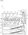
- the image forming apparatus 10 shown in FIG. 1 is a printer.
- the image forming apparatus 10 may be a copy machine, a facsimile apparatus, a multifunction peripheral, or the like.
- the image forming apparatus 10 is an apparatus which forms, on a sheet material 9, an image based on print job data received from a terminal apparatus not shown.
- the sheet material 9 is a sheet-like medium on which an image is to be formed, such as paper, coated paper, a postcard, an envelope, or an OHP sheet.
- the image forming apparatus 10 includes sheet storage portions 30, a sheet conveying portion 3, an image forming portion 4, the laser scanning unit 5, a fixing device 6, and the like.
- Each sheet storage portion 30 stores therein a plurality of stacked sheet materials 9.
- a sending-out roller 31 sends out the sheet material 9 from the sheet storage portion 30 to a sheet conveying path 300. Further, a conveying roller 32 conveys the sheet material 9 along the sheet conveying path 300. Further, a discharge roller 33 discharges the sheet material 9 on which an image has been formed, from the outlet of the sheet conveying path 300 onto a discharge tray 101.
- the image forming portion 4 executes an image forming process of forming, on the sheet material 9, an image that corresponds to image data generated based on the print job data.
- the image forming apparatus 10 shown in FIG. 1 is a tandem-type image forming apparatus and is a color printer.
- the image forming portion 4 further includes an intermediate transfer belt 48, a secondary cleaning device 480, and a secondary transfer device 49.
- the image forming portion 4 includes a plurality of single-color image forming portions 4x that correspond to the respective colors of cyan, magenta, yellow, and black. Further, the image forming apparatus 10 includes a plurality of toner supply portions 40 which respectively supply later-described developing devices 43 with toners of the respective colors of cyan, magenta, yellow, and black.
- the conveying roller 32 conveys the sheet material 9 via the secondary transfer device 49 to the discharge outlet of the sheet conveying path 300.
- Each single-color image forming portion 4x includes: a photosensitive member 41 which carries a toner image; a charging device 42; a developing device 43; a primary transfer device 45; a primary cleaning device 47; and the like.
- the photosensitive member 41 is one example of an image carrier.
- the photosensitive member 41 rotates, and the charging device 42 uniformly charges the surface of the photosensitive member 41. Further, the laser scanning unit 5 performs scanning with laser light 7, thereby writing an electrostatic latent image on the charged surface of the photosensitive member 41.
- the laser scanning unit 5 includes a scanner 5a such as a polygon mirror which performs scanning with the laser light 7.
- the laser scanning unit 5 also includes an f ⁇ lens 5b and the like.
- the laser scanning unit 5 includes: a light source unit 50 which outputs the laser light 7; a scanning unit 5x which includes a scanner 5a and the f ⁇ lens 5b.
- the scanning unit 5x performs scanning with the laser light 7 outputted from the light source unit 50.
- the electrostatic latent image is formed on the surface of the photosensitive member 41 by the laser light 7 outputted from the laser scanning unit 5.
- the light source unit 50 and the scanning unit may be integrally formed.
- the developing device 43 supplies the toner to the photosensitive member 41, thereby developing the electrostatic latent image into a toner image.
- the toner is supplied from the toner supply portion 40 to the developing device 43.
- the primary transfer device 45 transfers the toner image on the surface of the photosensitive member 41 to the intermediate transfer belt 48.
- the primary cleaning device 47 removes the toner remaining on the surface of the photosensitive member 41.
- the intermediate transfer belt 48 is an endless belt-like member formed in a loop shape.
- the intermediate transfer belt 48 rotates in a state of being extended on and between two rollers.
- each single-color image forming portion 4x forms an image of its corresponding color on the surface of the rotating intermediate transfer belt 48. Accordingly, a color image in which images of the respective colors are superposed is formed on the intermediate transfer belt 48.
- the secondary transfer device 49 transfers the toner image formed on the intermediate transfer belt 48, onto the sheet material 9.
- the primary transfer device 45, the intermediate transfer belt 48, and the secondary transfer device 49 represent one example of a transfer device which transfers the toner image on the photosensitive member 41 onto the sheet material 9.
- the secondary cleaning device 480 removes the toner remaining on the portion, of the intermediate transfer belt 48, which has passed through the secondary transfer device 49.
- the fixing device 6 sends out the sheet material 9 on which the image has been formed, while nipping the sheet material 9 between a heating roller 61 housing a heater and a pressure roller 62. By doing so, the fixing device 6 heats the toner on the sheet material 9 to fix the image on the sheet material 9.
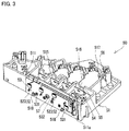
- FIGS. 2 and 3 are perspective views of the light source unit 50 viewed from different directions, respectively.
- the light source unit 50 includes a support body 51, a semiconductor laser element 52, a substrate 53, a collimator lens 54, an aperture 55, a mirror 56, and the like.
- the support body 51 is an integrally molded member made of a synthetic resin.
- the support body 51 may be an integrally molded member which is made of a synthetic resin and in which polycarbonate (PC) and polystyrene (PS) are mixed.
- PC polycarbonate
- PS polystyrene
- the light source unit 50 includes a plurality of the semiconductor laser elements 52. Each of the semiconductor laser elements 52 outputs the laser light 7 for writing the electrostatic latent image in its corresponding color of cyan, magenta, yellow, or black.
- FIG. 6 is a perspective view of the semiconductor laser element 52.
- the semiconductor laser element 52 includes a body portion 520, a flange portion 522, and terminals 523.
- a light emission hole 521 through which the laser light 7 is emitted is formed on the front face side of the body portion 520.
- the exterior members of the body portion 520 and the flange portion 522 are metal members.
- the flange portion 522 is a portion that protrudes outwardly from the body portion 520.
- the outer peripheral surface of the body portion 520 and the outer peripheral surface of the flange portion 522 are each in a cylindrical shape.
- the terminals 523 are formed so as to protrude on the rear face side of the semiconductor laser element 52.
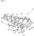
- the support body 51 includes a vertical wall portion 511 in which through-holes 5110 are formed (see FIGS. 2 to 4 ).
- the vertical wall portion 511 is a flat-plate-shaped portion that stands along the outer edge of the support body 51.
- Each semiconductor laser element 52 is press-fitted in its corresponding through-hole 5110 in the vertical wall portion 511.
- the substrate 53 is an electronic substrate to which the terminals 523 on the rear face side of each semiconductor laser element 52 are connected.
- the substrate 53 is located on a first face 511a side of the vertical wall portion 511.
- the first face 511a of the vertical wall portion 511 is the outer face of the support body 51.
- a second face 511b which is on the opposite side to the first face 511a of the vertical wall portion 511 is the inner face of the support body 51.
- two protruding portions 518 are formed on the first face 511a of the vertical wall portion 511. Further, in the vertical wall portion 511, a screw hole 511z into which a screw 57 is screwed from the first face 511a side is formed.
- the two protruding portions 518 on the vertical wall portion 511 are respectively fitted in two first through-holes 531 formed in the substrate 53. Further, a screw 57 is inserted into a second through-hole 532 formed in the substrate 53, to be screwed into the screw hole 511z in the vertical wall portion 511. Accordingly, the substrate 53 is mounted to the support body 51.
- the terminals 523 of each semiconductor laser element 52 pass through an installation hole in the substrate 53. Then, the terminals 523 of the semiconductor laser element 52 are fixed to the substrate 53 by soldering or the like.
- the collimator lens 54 is mounted to the support body 51 in the path of the laser light 7 emitted by the semiconductor laser element 52.
- a plurality of the collimator lenses 54 are mounted to the support body 51 at positions in front of the respective semiconductor laser elements 52 mounted to the vertical wall portion 511.
- each collimator lens 54 is mounted at a position on the second face 511b side of the vertical wall portion 511 in the support body 51.
- a seat 512 is formed at the position in the support body 51 where each collimator lens 54 is mounted.
- the collimator lens 54 is bonded to the seat 512 with an adhesive agent in a state of standing in front of the semiconductor laser element 52.
- the aperture 55 is mounted to the support body 51 in the path of the laser light 7 that has passed through the collimator lens 54.
- a plurality of the apertures 55 are mounted to the support body 51 at positions in front of the respective semiconductor laser elements 52 and beyond the collimator lenses 54.
- a pair of protruding portions 513 and a through-hole 5130 are formed (see FIGS. 2 , 4 , and 5 ).
- the pair of protruding portions 513 are fitted in a pair of holes formed in a seat portion of the aperture 55, and a protrusion formed in the seat portion of the aperture 55 is fitted in the through-hole 5130 in the support body 51.
- partition walls 515 are formed which partition the peripheries of the portions in each of which the collimator lens 54 and the aperture 55 are mounted.
- a cut-out portion 516 is formed which serves as the passage for the laser light 7 having passed through the aperture 55.
- An opening 514 is formed in a portion, of the support body 51, on the opposite side to the vertical wall portion 511 side relative to the seat 512.
- a plurality of the openings 514 are formed so as to correspond to the respective seats 512.
- each seat 512 is formed at the position in the support body 51 where the collimator lens 54 is mounted.
- a jig (not shown) holding the collimator lens 54 is passed through the opening 514. That is, the opening 514 is used in adjusting the mounting position of the collimator lens 54.
- the pair of protruding portions 513 are formed on opposite sides of the opening 514, respectively.
- the aperture 55 is mounted to the support body 51 so as to extend across the opening 514.
- FIG. 5 is a bottom view of the support body 51.
- the support body 51 is a member formed with a mold, with a position on the opposite side to the vertical wall portion 511 side relative to the openings 514 being set as the position for a resin flow-in gate G0.
- the resin in a fluid state starts to flow from the position of the resin flow-in gate G0, goes around both sides of the region of the opening 514, and then, flows into the region extending from the seats 512 to the vertical wall portion 511.
- the portion, of the support body 51, extending from the seats 512 to the vertical wall portion 511 is easy to be molded into a state of being easily shrinkable at an increased temperature, compared to the other portions of the support body 51.
- the mirror 56 is mounted to the support body 51 in the path of the laser light 7 having passed through the collimator lens 54 and the aperture 55.
- a plurality of the mirrors 56 are mounted to the support body 51 at positions in front of the respective semiconductor laser elements 52 and beyond the collimator lenses 54 and the apertures 55.
- the laser light 7 is incident obliquely to the reflection surface of the mirror 56, to be reflected to another direction.
- mirror receiving portions 517 are formed at positions in the support body 51 where the mirrors 56 are mounted, respectively.
- Each mirror 56 is fixed to the support body 51 with a screw or the like, in a state where the reflection surface of the mirror 56 is pushed against the mirror receiving portion 517.
- the mirror 56 is mounted to the support body 51 in a state where the reflection surface of the mirror 56 faces a predetermined direction.
- the through-holes 5110 in the vertical wall portion 511 are formed at positions at different heights, respectively. That is, the respective semiconductor laser elements 52 are mounted at positions at different heights in the vertical wall portion 511.
- the plurality of the laser lights 7 having been reflected at the respective mirrors 56 are arranged in a line in the vertical direction.
- other optical devices are also mounted to the support body 51.
- the temperature around the light source unit 50 in the image forming apparatus 10 tends to be high due to heat generated by the semiconductor laser elements 52, heat generated by a heater of the fixing device 6, and the like.
- the support body 51, made of a synthetic resin, of the light source unit 50 could shrink and deform over time due to continuous use thereof in a high temperature environment.
- the support body 51 of the light source unit 50 shrinks, the distance from the semiconductor laser element 52 to the collimator lens 54 is decreased. Then, the focus position of the laser light 7 on the surface of the photosensitive member 41 changes, and such change in the focus position could cause deterioration of image quality.
- FIGS. 7 and 8 are each a vertical cross-sectional view of the semiconductor laser element 52 and the portion of the through-hole 5110 in the support body 51 of the light source unit 50.
- FIG. 7 shows a state before the semiconductor laser element 52 is press-fitted into the through-hole 5110 in the support body 51.
- FIG. 8 shows a state where the semiconductor laser element 52 has been press-fitted in the through-hole 5110 in the support body 51.
- the through-hole 5110 in the vertical wall portion 511 includes an externally-contacting hole portion 511x which comes into contact with the outer peripheral surface of the flange portion 522 of the semiconductor laser element 52.
- the transverse sectional shape of the inner peripheral surface of the externally-contacting hole portion 511x is analogous to the transverse sectional shape of the outer peripheral surface of the flange portion 522.
- the inner peripheral surface of the externally-contacting hole portion 511x is in a cylindrical shape.
- a part on the first face 511a side of the through-hole 5110 in the vertical wall portion 511 is a guide-in hole portion 511y formed so as to have an inner diameter greater than the outer diameter of the flange portion 522.
- the flange portion 522 of the semiconductor laser element 52 is press-fitted, with the front face of the semiconductor laser element 52 serving as the leading head, into the externally-contacting hole portion 511x from the first face 511a side of the vertical wall portion 511.
- the inner diameter of the externally-contacting hole portion 511x is slightly smaller than the outer diameter of the flange portion 522.
- the flange portion 522 made of a metal has a higher rigidity than the externally-contacting hole portion 511x made of a synthetic resin.
- the edge portion, of the flange portion 522, on the front face side of the semiconductor laser element 52 will be referred to as a first edge portion 522x.
- the edge portion, of the flange portion 522, on the rear face side of the semiconductor laser element 52 will be referred to as a second edge portion 522y.
- the flange portion 522 is press-fitted into the externally-contacting hole portion 511x up to a middle position thereof, from the first face 511a side of the vertical wall portion 511. That is, the flange portion 522 is press-fitted in the externally-contacting hole portion 511x in a state where the first edge portion 522x of the flange portion 522 rests within the externally-contacting hole portion 511x.
- a small step 511s caused by the press-fitting of the flange portion 522 is formed on the inner surface of the externally-contacting hole portion 511x.
- the step 511s is formed at a portion, of the inner surface of the externally-contacting hole portion 511x, that is opposed to the first edge portion 522x of the flange portion 522.
- This step 511s is the evidence that the flange portion 522 has been press-fitted, with the front face of the semiconductor laser element 52 serving as the leading head, into the externally-contacting hole portion 511x from the first face 511a side of the vertical wall portion 511.
- the second edge portion 522y of the flange portion 522 is located to the first face 511a side of the vertical wall portion 511 relative to the externally-contacting hole portion 511x. That is, the second edge portion 522y is exposed on the first face 511a side of the vertical wall portion 511, from the externally-contacting hole portion 511x.
- S1, S2, ⁇ respectively represent identification signs of assembling steps of the light source unit 50.
- the assembling steps of the light source unit 50 are steps of assembling components to the support body 51.
- the assembling steps of the light source unit 50 are part of a method for manufacturing the laser scanning unit 5.
- the support body 51 formed with a mold is prepared. As described above, in the support body 51, the vertical wall portion 511, the through-holes 5110, the seats 512, the openings 514, and the like are formed.
- each semiconductor laser element 52 is press-fitted into its corresponding externally-contacting hole portion 511x of the through-hole 5110 in the vertical wall portion 511 of the support body 51.
- the flange portion 522 is press-fitted, with the front face of the semiconductor laser element 52 serving as the leading head, into the externally-contacting hole portion 511x from the first face 511a side of the vertical wall portion 511 (see FIGS. 7 and 8 ).
- step S2 the press-fitting of the flange portion 522 into the externally-contacting hole portion 511x is stopped at a position where the first edge portion 522x of the flange portion 522 rests within the externally-contacting hole portion 511x. That is, the step of pushing the flange portion 522 into the externally-contacting hole portion 511x from the first face 511a side ends before the first edge portion 522x of the flange portion 522 passes through the externally-contacting hole portion 511x. Accordingly, the small step 511s is formed on the inner surface of the externally-contacting hole portion 511x (see FIG. 8 ).
- the press-fitting of the flange portion 522 into the externally-contacting hole portion 511x is stopped at a position where the second edge portion 522y of the flange portion 522 does not reach the externally-contacting hole portion 511x.
- the second edge portion 522y of the flange portion 522 is located to the first face 511a side of the vertical wall portion 511 relative to the externally-contacting hole portion 511x.
- the substrate 53 is mounted, on the first face 511a side, to the vertical wall portion 511 of the support body 51.
- the two protruding portions 518 of the vertical wall portion 511 are fitted into the two first through-holes 531 in the substrate 53, respectively (see FIG. 3 ). Accordingly, the position of the substrate 53 relative to the vertical wall portion 511 is fixed. At that time, the terminals 523 of each semiconductor laser element 52 pass through the installation hole in the substrate 53. Further, the substrate 53 is fixed, on the first face 511a side, to the vertical wall portion 511 with the screw 57 (see FIG. 3 ).
- the terminals 523 on the rear face side of the semiconductor laser element 52 are connected to the wiring pattern of the substrate 53 by soldering.
- each collimator lens 54 is mounted on the seat 512 in the support body 51.
- the collimator lens 54 is bonded to the seat 512 with an adhesive agent.
- the position and the orientation of the collimator lens 54 are adjusted in a state where a jig (not shown) holding the collimator lens 54 is passed through the opening 514 of the support body 51.
- the collimator lens 54 is mounted to the support body 51, in the path of emitted light from the front face of the semiconductor laser element 52 on the second face 511b side of the vertical wall portion 511.
- optical devices such as the apertures 55 and the mirrors 56 are mounted to the support body 51.
- the assembling steps of the light source unit 50 also include steps not described in the above, description thereof is omitted here.
- one or both of the step (S5) of mounting each collimator lens 54 to the support body 51, and the step (S6) of mounting optical devices such as the apertures 55 to the support body 51 may be executed before the step (S2) of press-fitting the flange portion 522 into the externally-contacting hole portion 511x.
- FIG. 10 shows mounting methods of the semiconductor laser elements 52 according to four comparative examples EX1 to EX4 in the evaluation test.
- each arrow indicates the direction along which the semiconductor laser element 52 is press-fitted.
- First comparative example EX1 is an example in which, as in the case of the light source unit 50, the flange portion 522 has been press-fitted, with the front face of the semiconductor laser element 52 serving as the leading head, into the externally-contacting hole portion 511x from the first face 511a side of the vertical wall portion 511.
- First comparative example EX1 the press-fitting of the flange portion 522 into the externally-contacting hole portion 511x is performed up to a position where the first edge portion 522x of the flange portion 522 passes through the externally-contacting hole portion 511x.
- the flange portion 522 is press-fitted in the externally-contacting hole portion 511x in a state where the first edge portion 522x of the flange portion 522 protrudes to the second face 511b side from the externally-contacting hole portion 511x.
- Second comparative example EX2 is an example in which, as in the case of the light source unit 50, the flange portion 522 has been press-fitted, with the front face of the semiconductor laser element 52 serving as the leading head, into the externally-contacting hole portion 511x from the first face 511a side of the vertical wall portion 511.
- Second comparative example EX2 the flange portion 522 is press-fitted in the externally-contacting hole portion 511x in a state where the first edge portion 522x of the flange portion 522 rests within the externally-contacting hole portion 511x. This point is also the same as in the case of the light source unit 50.
- Second comparative example EX2 the second edge portion 522y of the flange portion 522 is bonded to the vertical wall portion 511 with an adhesive agent 5B.
- Third comparative example EX3 is an example in which the flange portion 522 has been press-fitted, with the rear face of the semiconductor laser element 52 serving as the leading head, into the externally-contacting hole portion 511x from the second face 511b side of the vertical wall portion 511.
- the flange portion 522 is press-fitted in the externally-contacting hole portion 511x in a state where the second edge portion 522y of the flange portion 522 rests within the externally-contacting hole portion 511x.
- Fourth comparative example EX4 is an example in which the step of press-fitting the flange portion 522 into the externally-contacting hole portion 511x has been executed a plurality of times, both in the direction from the first face 511a side to the second face 511b side of the vertical wall portion 511 and in the direction reverse thereto.
- FIG. 11 shows a result of an evaluation test which was conducted regarding the light source unit 50 and the light source units of the respective four comparative examples EX1 to EX4.
- EX0 indicates the evaluation result of the light source unit 50.
- the evaluation test is an acceleration test regarding use of the light source units in a high temperature environment.
- each light source unit is placed in a thermostat at 60°C for 60 hours. As a result of this, shrinkage of the support body 51 occurs. Then, the focus change amount in the main scanning direction of the laser light 7 emitted by each light source unit is measured.
- a longitudinal magnification ⁇ of the laser light 7 is 565.
- the focal length relative to the collimator lens 54 is Fco
- the focal length of the f ⁇ lens 5b is F ⁇
- FIG. 11 shows a measurement result of the evaluation test.
- the focus change amount exceeds a threshold value P0, visible deterioration appears on the image formed on the sheet material 9.
- the focus change amount in the comparative example EX1 is greater than that of the light source unit 50, but is smaller than the threshold value P0 at which image deterioration appears.
- the focus change amount of each of the comparative examples EX2 to EX4 is greater than the threshold value P0.
- the focus change amount of the laser light 7 can be suppressed at a small level compared to those in the comparative examples EX1 to EX4.
- the distance between the vertical wall portion 511 and the collimator lens 54 is reduced. It is estimated that, at that time, the semiconductor laser element 52 withdraws to the first face 511a side of the vertical wall portion 511 in the externally-contacting hole portion 511x, in response to the shrinkage of the support body 51.
- the withdrawal of the semiconductor laser element 52 acts in the direction which allows the distance between the semiconductor laser element 52 and the collimator lens 54 to be kept constant. This fact is estimated to be the factor for the good result of the light source unit 50 in the evaluation test.
- the longitudinal magnification ⁇ is 500
- the focus change amount at the time when the distance between the semiconductor laser element 52 and the collimator lens 54 has changed by 1 micrometer is 5 times of that in the case where the longitudinal magnification ⁇ is 100.
- the longitudinal magnification ⁇ exceeds 300, the effect realized by employing the light source unit 50 becomes more significant.
- the method for manufacturing the light source unit, the light source unit, and the image forming apparatus according to the present disclosure can also be configured by freely combining the embodiment and application examples described above, or modifying or partially omitting the embodiment and application examples as appropriate, within the scope of the disclosure recited in each claim.
Landscapes
- Physics & Mathematics (AREA)
- General Physics & Mathematics (AREA)
- Optics & Photonics (AREA)
- Condensed Matter Physics & Semiconductors (AREA)
- Electromagnetism (AREA)
- Laser Beam Printer (AREA)
- Semiconductor Lasers (AREA)
- Facsimile Scanning Arrangements (AREA)
- Mechanical Optical Scanning Systems (AREA)
Abstract
Description
- The present disclosure relates to a method for manufacturing a laser scanning unit, the laser scanning unit, and an image forming apparatus provided with the same.
- In general, an electrophotographic type image forming apparatus includes a laser scanning unit which emits laser light for writing an electrostatic latent image on a surface of an image carrier. The laser scanning unit includes: optical components such as a semiconductor laser element and a collimator lens; and a support body which is made of a synthetic resin and to which the optical components are mounted.
- A method for manufacturing a laser scanning unit according to one aspect of the present disclosure includes the following components. The laser scanning unit includes a support body, a semiconductor laser element, a substrate, and a collimator lens. The support body is an integrally molded member made of a synthetic resin and has a vertical wall portion in which a through-hole is formed. The semiconductor laser element has a flange portion protruding outwardly from a body portion thereof. The manufacturing method includes press-fitting the flange portion, with a front face of the semiconductor laser element serving as a leading head, into an externally-contacting hole portion of the through-hole in the vertical wall portion from a first face side of the vertical wall portion, the externally-contacting hole portion being configured to come into contact with an outer peripheral surface of the flange portion. Further, the manufacturing method includes installing a terminal on a rear face side of the semiconductor laser element to the substrate. Further, the manufacturing method includes mounting the collimator lens to the support body before or after the flange portion of the semiconductor laser element is press-fitted into the externally-contacting hole portion. The press-fitting of the flange portion into the externally-contacting hole portion is stopped at a position where an edge portion, of the flange portion, on the front face side of the semiconductor laser element rests within the externally-contacting hole portion. The collimator lens is mounted to the support body in a path of emitted light in front of the semiconductor laser element.
- A laser scanning unit according to another aspect of the present disclosure includes a support body, a semiconductor laser element, a substrate, and a collimator lens. The support body is an integrally molded member made of a synthetic resin and has a vertical wall portion in which a through-hole is formed. The semiconductor laser element is press-fitted in the through-hole in the vertical wall portion. The substrate is located on a first face side of the vertical wall portion, and a terminal on a rear face side of the semiconductor laser element is installed to the substrate. The collimator lens is mounted to the support body in a path of emitted light in front of the semiconductor laser element. The semiconductor laser element has a flange portion protruding outwardly from a body portion thereof. The through-hole in the vertical wall portion includes an externally-contacting hole portion configured to come into contact with an outer peripheral surface of the flange portion. The flange portion is press-fitted in the externally-contacting hole portion of the vertical wall portion in a state where an edge portion, of the flange portion, on a front face side of the semiconductor laser element rests within the externally-contacting hole portion. A step is formed on an inner surface of the externally-contacting hole portion, the step being generated as a result of the flange portion having been press-fitted, with a front face of the semiconductor laser element serving as a leading head, into the externally-contacting hole portion from the first face side of the vertical wall portion.
- An image forming apparatus according to another aspect of the present disclosure includes the laser scanning unit, an image carrier, a developing device, and a transfer device. On the image carrier, an electrostatic latent image is formed by laser light outputted from the laser scanning unit. The developing device is a device configured to develop the electrostatic latent image into a toner image. The transfer device is a device configured to transfer the toner image to a sheet material.
- This Summary is provided to introduce a selection of concepts in a simplified form that are further described below in the Detailed Description with reference where appropriate to the accompanying drawings. This Summary is not intended to identify key features or essential features of the claimed subject matter, nor is it intended to be used to limit the scope of the claimed subject matter. Furthermore, the claimed subject matter is not limited to implementations that solve any or all disadvantages noted in any part of this disclosure.
-
-
FIG. 1 is a configuration diagram of an image forming apparatus including a laser scanning unit according to an embodiment. -
FIG. 2 is a first perspective view of a light source unit included in the laser scanning unit according to the embodiment. -
FIG. 3 is a second perspective view of the light source unit included in the laser scanning unit according to the embodiment. -
FIG. 4 is a perspective view of a support body included in the light source unit. -
FIG. 5 is a bottom view of the support body included in the light source unit. -
FIG. 6 is a perspective view of a semiconductor laser element. -
FIG. 7 is a cross-sectional view of a part of the support body of the light source unit included in the laser scanning unit according to the embodiment and the semiconductor laser element before being press-fitted into a through-hole in the support body. -
FIG. 8 is a cross-sectional view of a part of the support body of the light source unit included in the laser scanning unit according to the embodiment and the semiconductor laser element having been press-fitted in a through-hole in the support body. -
FIG. 9 is a flow chart showing one example of a manufacturing procedure of the light source unit included in the laser scanning unit according to the embodiment. -
FIG. 10 shows mounting methods of semiconductor laser elements according to comparative examples in an evaluation test, in whichFIG. 10A shows First comparative example,FIG. 10B shows Second comparative example,FIG. 10C shows Third comparative example, andFIG. 10D shows Fourth comparative example. -
FIG. 11 is a graph showing a result of the evaluation test. - Hereinafter, embodiments of the present disclosure will be described with reference to the accompanying drawings. The embodiments described below represent an exemplary implementation of the present disclosure, and the technical scope of the present disclosure is not limited to the embodiments described below.
- First, with reference to
FIG. 1 , a configuration of an electrophotographic typeimage forming apparatus 10 which includes alaser scanning unit 5 according to an embodiment will be described. Theimage forming apparatus 10 shown inFIG. 1 is a printer. Theimage forming apparatus 10 may be a copy machine, a facsimile apparatus, a multifunction peripheral, or the like. - The
image forming apparatus 10 is an apparatus which forms, on asheet material 9, an image based on print job data received from a terminal apparatus not shown. Thesheet material 9 is a sheet-like medium on which an image is to be formed, such as paper, coated paper, a postcard, an envelope, or an OHP sheet. - The
image forming apparatus 10 includessheet storage portions 30, asheet conveying portion 3, animage forming portion 4, thelaser scanning unit 5, afixing device 6, and the like. Eachsheet storage portion 30 stores therein a plurality of stackedsheet materials 9. - In the
sheet conveying portion 3, a sending-out roller 31 sends out thesheet material 9 from thesheet storage portion 30 to asheet conveying path 300. Further, aconveying roller 32 conveys thesheet material 9 along thesheet conveying path 300. Further, adischarge roller 33 discharges thesheet material 9 on which an image has been formed, from the outlet of thesheet conveying path 300 onto adischarge tray 101. - The
image forming portion 4 executes an image forming process of forming, on thesheet material 9, an image that corresponds to image data generated based on the print job data. Theimage forming apparatus 10 shown inFIG. 1 is a tandem-type image forming apparatus and is a color printer. Thus, theimage forming portion 4 further includes anintermediate transfer belt 48, asecondary cleaning device 480, and asecondary transfer device 49. - The
image forming portion 4 includes a plurality of single-colorimage forming portions 4x that correspond to the respective colors of cyan, magenta, yellow, and black. Further, theimage forming apparatus 10 includes a plurality oftoner supply portions 40 which respectively supply later-described developingdevices 43 with toners of the respective colors of cyan, magenta, yellow, and black. - In the
sheet conveying portion 3, the conveyingroller 32 conveys thesheet material 9 via thesecondary transfer device 49 to the discharge outlet of thesheet conveying path 300. - Each single-color
image forming portion 4x includes: aphotosensitive member 41 which carries a toner image; a chargingdevice 42; a developingdevice 43; aprimary transfer device 45; aprimary cleaning device 47; and the like. Thephotosensitive member 41 is one example of an image carrier. - The
photosensitive member 41 rotates, and the chargingdevice 42 uniformly charges the surface of thephotosensitive member 41. Further, thelaser scanning unit 5 performs scanning withlaser light 7, thereby writing an electrostatic latent image on the charged surface of thephotosensitive member 41. Thelaser scanning unit 5 includes ascanner 5a such as a polygon mirror which performs scanning with thelaser light 7. Thelaser scanning unit 5 also includes anfθ lens 5b and the like. - The
laser scanning unit 5 includes: alight source unit 50 which outputs thelaser light 7; ascanning unit 5x which includes ascanner 5a and thefθ lens 5b. Thescanning unit 5x performs scanning with thelaser light 7 outputted from thelight source unit 50. The electrostatic latent image is formed on the surface of thephotosensitive member 41 by thelaser light 7 outputted from thelaser scanning unit 5. Thelight source unit 50 and the scanning unit may be integrally formed. - The developing
device 43 supplies the toner to thephotosensitive member 41, thereby developing the electrostatic latent image into a toner image. The toner is supplied from thetoner supply portion 40 to the developingdevice 43. - Further, the
primary transfer device 45 transfers the toner image on the surface of thephotosensitive member 41 to theintermediate transfer belt 48. Theprimary cleaning device 47 removes the toner remaining on the surface of thephotosensitive member 41. - The
intermediate transfer belt 48 is an endless belt-like member formed in a loop shape. Theintermediate transfer belt 48 rotates in a state of being extended on and between two rollers. In theimage forming portion 4, each single-colorimage forming portion 4x forms an image of its corresponding color on the surface of the rotatingintermediate transfer belt 48. Accordingly, a color image in which images of the respective colors are superposed is formed on theintermediate transfer belt 48. - The
secondary transfer device 49 transfers the toner image formed on theintermediate transfer belt 48, onto thesheet material 9. In the present embodiment, theprimary transfer device 45, theintermediate transfer belt 48, and thesecondary transfer device 49 represent one example of a transfer device which transfers the toner image on thephotosensitive member 41 onto thesheet material 9. - The
secondary cleaning device 480 removes the toner remaining on the portion, of theintermediate transfer belt 48, which has passed through thesecondary transfer device 49. - The fixing
device 6 sends out thesheet material 9 on which the image has been formed, while nipping thesheet material 9 between aheating roller 61 housing a heater and apressure roller 62. By doing so, the fixingdevice 6 heats the toner on thesheet material 9 to fix the image on thesheet material 9. - Next, with reference to
FIGS. 2 to 6 , a configuration of thelight source unit 50 will be described.FIGS. 2 and3 are perspective views of thelight source unit 50 viewed from different directions, respectively. - The
light source unit 50 includes asupport body 51, asemiconductor laser element 52, asubstrate 53, acollimator lens 54, anaperture 55, amirror 56, and the like. - The
support body 51 is an integrally molded member made of a synthetic resin. For example, thesupport body 51 may be an integrally molded member which is made of a synthetic resin and in which polycarbonate (PC) and polystyrene (PS) are mixed. - The
light source unit 50 includes a plurality of thesemiconductor laser elements 52. Each of thesemiconductor laser elements 52 outputs thelaser light 7 for writing the electrostatic latent image in its corresponding color of cyan, magenta, yellow, or black. -
FIG. 6 is a perspective view of thesemiconductor laser element 52. Thesemiconductor laser element 52 includes abody portion 520, aflange portion 522, andterminals 523. Alight emission hole 521 through which thelaser light 7 is emitted is formed on the front face side of thebody portion 520. The exterior members of thebody portion 520 and theflange portion 522 are metal members. - In the
semiconductor laser element 52, theflange portion 522 is a portion that protrudes outwardly from thebody portion 520. In the present embodiment, the outer peripheral surface of thebody portion 520 and the outer peripheral surface of theflange portion 522 are each in a cylindrical shape. Theterminals 523 are formed so as to protrude on the rear face side of thesemiconductor laser element 52. - The
support body 51 includes avertical wall portion 511 in which through-holes 5110 are formed (seeFIGS. 2 to 4 ). In the example shown inFIG. 4 , thevertical wall portion 511 is a flat-plate-shaped portion that stands along the outer edge of thesupport body 51. Eachsemiconductor laser element 52 is press-fitted in its corresponding through-hole 5110 in thevertical wall portion 511. - The
substrate 53 is an electronic substrate to which theterminals 523 on the rear face side of eachsemiconductor laser element 52 are connected. Thesubstrate 53 is located on afirst face 511a side of thevertical wall portion 511. Thefirst face 511a of thevertical wall portion 511 is the outer face of thesupport body 51. Asecond face 511b which is on the opposite side to thefirst face 511a of thevertical wall portion 511 is the inner face of thesupport body 51. - In the example shown in
FIG. 4 , two protrudingportions 518 are formed on thefirst face 511a of thevertical wall portion 511. Further, in thevertical wall portion 511, ascrew hole 511z into which ascrew 57 is screwed from thefirst face 511a side is formed. - As shown in
FIGS. 3 and4 , the two protrudingportions 518 on thevertical wall portion 511 are respectively fitted in two first through-holes 531 formed in thesubstrate 53. Further, ascrew 57 is inserted into a second through-hole 532 formed in thesubstrate 53, to be screwed into thescrew hole 511z in thevertical wall portion 511. Accordingly, thesubstrate 53 is mounted to thesupport body 51. - When the
substrate 53 is to be mounted to thesupport body 51, theterminals 523 of eachsemiconductor laser element 52 pass through an installation hole in thesubstrate 53. Then, theterminals 523 of thesemiconductor laser element 52 are fixed to thesubstrate 53 by soldering or the like. - The
collimator lens 54 is mounted to thesupport body 51 in the path of thelaser light 7 emitted by thesemiconductor laser element 52. A plurality of thecollimator lenses 54 are mounted to thesupport body 51 at positions in front of the respectivesemiconductor laser elements 52 mounted to thevertical wall portion 511. - That is, each
collimator lens 54 is mounted at a position on thesecond face 511b side of thevertical wall portion 511 in thesupport body 51. - In the present embodiment, a
seat 512 is formed at the position in thesupport body 51 where eachcollimator lens 54 is mounted. Thecollimator lens 54 is bonded to theseat 512 with an adhesive agent in a state of standing in front of thesemiconductor laser element 52. - The
aperture 55 is mounted to thesupport body 51 in the path of thelaser light 7 that has passed through thecollimator lens 54. A plurality of theapertures 55 are mounted to thesupport body 51 at positions in front of the respectivesemiconductor laser elements 52 and beyond thecollimator lenses 54. - In the present embodiment, at the position in the
support body 51 where eachaperture 55 is mounted, a pair of protrudingportions 513 and a through-hole 5130 are formed (seeFIGS. 2 ,4 , and5 ). The pair of protrudingportions 513 are fitted in a pair of holes formed in a seat portion of theaperture 55, and a protrusion formed in the seat portion of theaperture 55 is fitted in the through-hole 5130 in thesupport body 51. - In the
support body 51,partition walls 515 are formed which partition the peripheries of the portions in each of which thecollimator lens 54 and theaperture 55 are mounted. In eachpartition wall 515, a cut-outportion 516 is formed which serves as the passage for thelaser light 7 having passed through theaperture 55. - An
opening 514 is formed in a portion, of thesupport body 51, on the opposite side to thevertical wall portion 511 side relative to theseat 512. In thesupport body 51, a plurality of theopenings 514 are formed so as to correspond to therespective seats 512. As described above, eachseat 512 is formed at the position in thesupport body 51 where thecollimator lens 54 is mounted. - When the position and the orientation of the
collimator lens 54 on theseat 512 are adjusted, a jig (not shown) holding thecollimator lens 54 is passed through theopening 514. That is, theopening 514 is used in adjusting the mounting position of thecollimator lens 54. - The pair of protruding
portions 513 are formed on opposite sides of theopening 514, respectively. Theaperture 55 is mounted to thesupport body 51 so as to extend across theopening 514. -
FIG. 5 is a bottom view of thesupport body 51. Thesupport body 51 is a member formed with a mold, with a position on the opposite side to thevertical wall portion 511 side relative to theopenings 514 being set as the position for a resin flow-in gate G0. Thus, when thesupport body 51 is to be formed with a mold, the resin in a fluid state starts to flow from the position of the resin flow-in gate G0, goes around both sides of the region of theopening 514, and then, flows into the region extending from theseats 512 to thevertical wall portion 511. - The portion, of the
support body 51, extending from theseats 512 to thevertical wall portion 511 is easy to be molded into a state of being easily shrinkable at an increased temperature, compared to the other portions of thesupport body 51. - The
mirror 56 is mounted to thesupport body 51 in the path of thelaser light 7 having passed through thecollimator lens 54 and theaperture 55. A plurality of themirrors 56 are mounted to thesupport body 51 at positions in front of the respectivesemiconductor laser elements 52 and beyond thecollimator lenses 54 and theapertures 55. Thelaser light 7 is incident obliquely to the reflection surface of themirror 56, to be reflected to another direction. - In the present embodiment,
mirror receiving portions 517 are formed at positions in thesupport body 51 where themirrors 56 are mounted, respectively. Eachmirror 56 is fixed to thesupport body 51 with a screw or the like, in a state where the reflection surface of themirror 56 is pushed against themirror receiving portion 517. As a result of this, themirror 56 is mounted to thesupport body 51 in a state where the reflection surface of themirror 56 faces a predetermined direction. - In the present embodiment, the through-
holes 5110 in thevertical wall portion 511 are formed at positions at different heights, respectively. That is, the respectivesemiconductor laser elements 52 are mounted at positions at different heights in thevertical wall portion 511. - The plurality of the
laser lights 7 having been reflected at therespective mirrors 56 are arranged in a line in the vertical direction. To thesupport body 51, other optical devices are also mounted. - Meanwhile, the temperature around the
light source unit 50 in theimage forming apparatus 10 tends to be high due to heat generated by thesemiconductor laser elements 52, heat generated by a heater of the fixingdevice 6, and the like. In addition, thesupport body 51, made of a synthetic resin, of thelight source unit 50 could shrink and deform over time due to continuous use thereof in a high temperature environment. - In the
image forming apparatus 10, if thesupport body 51 of thelight source unit 50 shrinks, the distance from thesemiconductor laser element 52 to thecollimator lens 54 is decreased. Then, the focus position of thelaser light 7 on the surface of thephotosensitive member 41 changes, and such change in the focus position could cause deterioration of image quality. - On the other hand, in a case where the
light source unit 50 is employed, even if thesupport body 51 made of a synthetic resin has shrunk over time, change in the focus position of thelaser light 7 outputted by thelight source unit 50 can be suppressed to the minimum level. This will be explained below. - Hereinafter, with reference to
FIGS. 7 and 8 , a mounting structure for thesemiconductor laser element 52 will be described.FIGS. 7 and 8 are each a vertical cross-sectional view of thesemiconductor laser element 52 and the portion of the through-hole 5110 in thesupport body 51 of thelight source unit 50.FIG. 7 shows a state before thesemiconductor laser element 52 is press-fitted into the through-hole 5110 in thesupport body 51.FIG. 8 shows a state where thesemiconductor laser element 52 has been press-fitted in the through-hole 5110 in thesupport body 51. - The through-
hole 5110 in thevertical wall portion 511 includes an externally-contactinghole portion 511x which comes into contact with the outer peripheral surface of theflange portion 522 of thesemiconductor laser element 52. The transverse sectional shape of the inner peripheral surface of the externally-contactinghole portion 511x is analogous to the transverse sectional shape of the outer peripheral surface of theflange portion 522. In the present embodiment, the inner peripheral surface of the externally-contactinghole portion 511x is in a cylindrical shape. - In the present embodiment, a part on the
first face 511a side of the through-hole 5110 in thevertical wall portion 511 is a guide-inhole portion 511y formed so as to have an inner diameter greater than the outer diameter of theflange portion 522. - As shown in
FIG. 7 , theflange portion 522 of thesemiconductor laser element 52 is press-fitted, with the front face of thesemiconductor laser element 52 serving as the leading head, into the externally-contactinghole portion 511x from thefirst face 511a side of thevertical wall portion 511. - In a state before the
semiconductor laser element 52 is press-fitted into the externally-contactinghole portion 511x, the inner diameter of the externally-contactinghole portion 511x is slightly smaller than the outer diameter of theflange portion 522. Theflange portion 522 made of a metal has a higher rigidity than the externally-contactinghole portion 511x made of a synthetic resin. Thus, when theflange portion 522 is pushed into the externally-contactinghole portion 511x, the portion, of the inner surface of the externally-contactinghole portion 511x, that comes into contact with theflange portion 522 is expanded to have the same diameter as the outer diameter of theflange portion 522. - In the description below, the edge portion, of the
flange portion 522, on the front face side of thesemiconductor laser element 52 will be referred to as afirst edge portion 522x. The edge portion, of theflange portion 522, on the rear face side of thesemiconductor laser element 52 will be referred to as asecond edge portion 522y. - As shown in
FIG. 8 , theflange portion 522 is press-fitted into the externally-contactinghole portion 511x up to a middle position thereof, from thefirst face 511a side of thevertical wall portion 511. That is, theflange portion 522 is press-fitted in the externally-contactinghole portion 511x in a state where thefirst edge portion 522x of theflange portion 522 rests within the externally-contactinghole portion 511x. - Therefore, a
small step 511s caused by the press-fitting of theflange portion 522 is formed on the inner surface of the externally-contactinghole portion 511x. Thestep 511s is formed at a portion, of the inner surface of the externally-contactinghole portion 511x, that is opposed to thefirst edge portion 522x of theflange portion 522. Thisstep 511s is the evidence that theflange portion 522 has been press-fitted, with the front face of thesemiconductor laser element 52 serving as the leading head, into the externally-contactinghole portion 511x from thefirst face 511a side of thevertical wall portion 511. - In the present embodiment, the
second edge portion 522y of theflange portion 522 is located to thefirst face 511a side of thevertical wall portion 511 relative to the externally-contactinghole portion 511x. That is, thesecond edge portion 522y is exposed on thefirst face 511a side of thevertical wall portion 511, from the externally-contactinghole portion 511x. - Next, with reference to the flow chart shown in
FIG. 9 , one example of the manufacturing procedure of thelight source unit 50 will be described. In the description below, S1, S2, ··· respectively represent identification signs of assembling steps of thelight source unit 50. The assembling steps of thelight source unit 50 are steps of assembling components to thesupport body 51. The assembling steps of thelight source unit 50 are part of a method for manufacturing thelaser scanning unit 5. - First, the
support body 51 formed with a mold is prepared. As described above, in thesupport body 51, thevertical wall portion 511, the through-holes 5110, theseats 512, theopenings 514, and the like are formed. - Next, the
flange portion 522 of eachsemiconductor laser element 52 is press-fitted into its corresponding externally-contactinghole portion 511x of the through-hole 5110 in thevertical wall portion 511 of thesupport body 51. At that time, theflange portion 522 is press-fitted, with the front face of thesemiconductor laser element 52 serving as the leading head, into the externally-contactinghole portion 511x from thefirst face 511a side of the vertical wall portion 511 (seeFIGS. 7 and 8 ). - In step S2, the press-fitting of the
flange portion 522 into the externally-contactinghole portion 511x is stopped at a position where thefirst edge portion 522x of theflange portion 522 rests within the externally-contactinghole portion 511x. That is, the step of pushing theflange portion 522 into the externally-contactinghole portion 511x from thefirst face 511a side ends before thefirst edge portion 522x of theflange portion 522 passes through the externally-contactinghole portion 511x. Accordingly, thesmall step 511s is formed on the inner surface of the externally-contactinghole portion 511x (seeFIG. 8 ). - In the present embodiment, the press-fitting of the
flange portion 522 into the externally-contactinghole portion 511x is stopped at a position where thesecond edge portion 522y of theflange portion 522 does not reach the externally-contactinghole portion 511x. Thus, thesecond edge portion 522y of theflange portion 522 is located to thefirst face 511a side of thevertical wall portion 511 relative to the externally-contactinghole portion 511x. - Next, the
substrate 53 is mounted, on thefirst face 511a side, to thevertical wall portion 511 of thesupport body 51. In this step, the two protrudingportions 518 of thevertical wall portion 511 are fitted into the two first through-holes 531 in thesubstrate 53, respectively (seeFIG. 3 ). Accordingly, the position of thesubstrate 53 relative to thevertical wall portion 511 is fixed. At that time, theterminals 523 of eachsemiconductor laser element 52 pass through the installation hole in thesubstrate 53. Further, thesubstrate 53 is fixed, on thefirst face 511a side, to thevertical wall portion 511 with the screw 57 (seeFIG. 3 ). - Then, the
terminals 523 on the rear face side of thesemiconductor laser element 52 are connected to the wiring pattern of thesubstrate 53 by soldering. - Further, each
collimator lens 54 is mounted on theseat 512 in thesupport body 51. In the present embodiment, thecollimator lens 54 is bonded to theseat 512 with an adhesive agent. - Further in this step, the position and the orientation of the
collimator lens 54 are adjusted in a state where a jig (not shown) holding thecollimator lens 54 is passed through theopening 514 of thesupport body 51. As a result of this, thecollimator lens 54 is mounted to thesupport body 51, in the path of emitted light from the front face of thesemiconductor laser element 52 on thesecond face 511b side of thevertical wall portion 511. - Further, other optical devices such as the
apertures 55 and themirrors 56 are mounted to thesupport body 51. - Although the assembling steps of the
light source unit 50 also include steps not described in the above, description thereof is omitted here. - In the assembling steps of the
light source unit 50, one or both of the step (S5) of mounting eachcollimator lens 54 to thesupport body 51, and the step (S6) of mounting optical devices such as theapertures 55 to thesupport body 51 may be executed before the step (S2) of press-fitting theflange portion 522 into the externally-contactinghole portion 511x. - Next, with reference to
FIGS. 10 and 11 , a result of an evaluation test which was conducted for comparing thelight source unit 50 with light source units of comparative examples will be described. -
FIG. 10 shows mounting methods of thesemiconductor laser elements 52 according to four comparative examples EX1 to EX4 in the evaluation test. InFIG. 10 , each arrow indicates the direction along which thesemiconductor laser element 52 is press-fitted. - First comparative example EX1 is an example in which, as in the case of the
light source unit 50, theflange portion 522 has been press-fitted, with the front face of thesemiconductor laser element 52 serving as the leading head, into the externally-contactinghole portion 511x from thefirst face 511a side of thevertical wall portion 511. - However, in First comparative example EX1, the press-fitting of the
flange portion 522 into the externally-contactinghole portion 511x is performed up to a position where thefirst edge portion 522x of theflange portion 522 passes through the externally-contactinghole portion 511x. As a result of this, theflange portion 522 is press-fitted in the externally-contactinghole portion 511x in a state where thefirst edge portion 522x of theflange portion 522 protrudes to thesecond face 511b side from the externally-contactinghole portion 511x. - Second comparative example EX2 is an example in which, as in the case of the
light source unit 50, theflange portion 522 has been press-fitted, with the front face of thesemiconductor laser element 52 serving as the leading head, into the externally-contactinghole portion 511x from thefirst face 511a side of thevertical wall portion 511. - Further, in Second comparative example EX2, the
flange portion 522 is press-fitted in the externally-contactinghole portion 511x in a state where thefirst edge portion 522x of theflange portion 522 rests within the externally-contactinghole portion 511x. This point is also the same as in the case of thelight source unit 50. - However, in Second comparative example EX2, the
second edge portion 522y of theflange portion 522 is bonded to thevertical wall portion 511 with anadhesive agent 5B. - Third comparative example EX3 is an example in which the
flange portion 522 has been press-fitted, with the rear face of thesemiconductor laser element 52 serving as the leading head, into the externally-contactinghole portion 511x from thesecond face 511b side of thevertical wall portion 511. - In Third comparative example EX3, the
flange portion 522 is press-fitted in the externally-contactinghole portion 511x in a state where thesecond edge portion 522y of theflange portion 522 rests within the externally-contactinghole portion 511x. - Fourth comparative example EX4 is an example in which the step of press-fitting the
flange portion 522 into the externally-contactinghole portion 511x has been executed a plurality of times, both in the direction from thefirst face 511a side to thesecond face 511b side of thevertical wall portion 511 and in the direction reverse thereto. - In Fourth comparative example EX4, when the
flange portion 522 is press-fitted into the externally-contactinghole portion 511x from thefirst face 511a side of thevertical wall portion 511, thefirst edge portion 522x passes through the externally-contactinghole portion 511x. Similarly, when theflange portion 522 is press-fitted into the externally-contactinghole portion 511x from thesecond face 511b side of thevertical wall portion 511, thesecond edge portion 522y passes through the externally-contactinghole portion 511x. Then, theflange portion 522 is held at a position where thefirst edge portion 522x protrudes to thesecond face 511b side from the externally-contactinghole portion 511x. -
FIG. 11 shows a result of an evaluation test which was conducted regarding thelight source unit 50 and the light source units of the respective four comparative examples EX1 to EX4. InFIG. 11 , EX0 indicates the evaluation result of thelight source unit 50. - The evaluation test is an acceleration test regarding use of the light source units in a high temperature environment. In the evaluation test, each light source unit is placed in a thermostat at 60°C for 60 hours. As a result of this, shrinkage of the
support body 51 occurs. Then, the focus change amount in the main scanning direction of thelaser light 7 emitted by each light source unit is measured. - In the evaluation test, a longitudinal magnification α of the
laser light 7 is 565. When the focal length relative to thecollimator lens 54 is Fco, and the focal length of thefθ lens 5b is Fθ, the longitudinal magnification α can be calculated by applying Fco and Fθ to a formula α = (Fco/Fθ)2. -
FIG. 11 shows a measurement result of the evaluation test. When the focus change amount exceeds a threshold value P0, visible deterioration appears on the image formed on thesheet material 9. - As shown in
FIG. 11 , the focus change amount in the comparative example EX1 is greater than that of thelight source unit 50, but is smaller than the threshold value P0 at which image deterioration appears. On the other hand, the focus change amount of each of the comparative examples EX2 to EX4 is greater than the threshold value P0. - If the
light source unit 50 is employed, even when thesupport body 51 made of a synthetic resin has shrunk over time in a high temperature environment, the focus change amount of thelaser light 7 can be suppressed at a small level compared to those in the comparative examples EX1 to EX4. - In the
light source unit 50, when thesupport body 51 has shrunk, the distance between thevertical wall portion 511 and thecollimator lens 54 is reduced. It is estimated that, at that time, thesemiconductor laser element 52 withdraws to thefirst face 511a side of thevertical wall portion 511 in the externally-contactinghole portion 511x, in response to the shrinkage of thesupport body 51. - The withdrawal of the
semiconductor laser element 52 acts in the direction which allows the distance between thesemiconductor laser element 52 and thecollimator lens 54 to be kept constant. This fact is estimated to be the factor for the good result of thelight source unit 50 in the evaluation test. - The greater the longitudinal magnification α of the
laser light 7 is, the higher the sensitivity to the focus change of thelaser light 7 is. For example, in a case where the longitudinal magnification α is 500, the focus change amount at the time when the distance between thesemiconductor laser element 52 and thecollimator lens 54 has changed by 1 micrometer is 5 times of that in the case where the longitudinal magnification α is 100. Thus, in such a case where the longitudinal magnification α exceeds 300, the effect realized by employing thelight source unit 50 becomes more significant. - The method for manufacturing the light source unit, the light source unit, and the image forming apparatus according to the present disclosure can also be configured by freely combining the embodiment and application examples described above, or modifying or partially omitting the embodiment and application examples as appropriate, within the scope of the disclosure recited in each claim.
- It is to be understood that the embodiments herein are illustrative and not restrictive, since the scope of the disclosure is defined by the appended claims rather than by the description preceding them, and all changes that fall within metes and bounds of the claims, or equivalence of such metes and bounds thereof are therefore intended to be embraced by the claims.
Claims (9)
- A method for manufacturing a laser scanning unit (5),
the laser scanning unit (5) including:a support body (51) being an integrally molded member made of a synthetic resin, and having a vertical wall portion (511) in which a through-hole (5110) is formed;a semiconductor laser element (52) having a flange portion (522) protruding outwardly from a body portion thereof;a substrate (53); anda collimator lens (54),the method comprising:press-fitting the flange portion (522), with a front face of the semiconductor laser element (52) serving as a leading head, into an externally-contacting hole portion (511x) of the through-hole (5110) in the vertical wall portion (511) from a first face side of the vertical wall portion (511), the externally-contacting hole portion (511x) being configured to come into contact with an outer peripheral surface of the flange portion (522);connecting a terminal on a rear face side of the semiconductor laser element (52) to the substrate (53); andmounting the collimator lens (54) to the support body (51) before or after the flange portion (522) of the semiconductor laser element (52) is press-fitted into the externally-contacting hole portion (511x), whereinthe press-fitting of the flange portion (522) into the externally-contacting hole portion (511x) is stopped at a position where an edge portion, of the flange portion (522), on the front face side of the semiconductor laser element (52) rests within the externally-contacting hole portion (511x), and
the collimator lens (54) is mounted to the support body (51) in a path of emitted light in front of the semiconductor laser element (52). - The method for manufacturing the laser scanning unit (5) according to claim 1, wherein
the press-fitting of the flange portion (522) into the externally-contacting hole portion (511x) is stopped at a position where an edge portion, of the flange portion (522), on the rear face side of the semiconductor laser element (52) does not reach the externally-contacting hole portion (511x). - The method for manufacturing the laser scanning unit (5) according to claim 1 or 2, wherein
an opening is formed in a portion, of the support body (51), on an opposite side to the vertical wall portion (511) side relative to a mounting position of the collimator lens (54), and
the support body (51) is a member formed with a mold, with a position on an opposite side to the vertical wall portion (511) side relative to the opening being set as a position for a resin flow-in gate. - The method for manufacturing the laser scanning unit (5) according to any one of claims 1 to 3, wherein
the support body (51) is an integrally molded member made of a synthetic resin in which polycarbonate and polystyrene are mixed. - A laser scanning unit (5) comprising:a support body (51) being an integrally molded member made of a synthetic resin, and having a vertical wall portion (511) in which a through-hole (5110) is formed;a semiconductor laser element (52) press-fitted in the through-hole (5110) in the vertical wall portion (511);a substrate (53) which is located on a first face side of the vertical wall portion (511), and to which a terminal on a rear face side of the semiconductor laser element (52) is connected; anda collimator lens (54) mounted to the support body (51) in a path of emitted light in front of the semiconductor laser element (52), whereinthe semiconductor laser element (52) has a flange portion (522) protruding outwardly from a body portion thereof,
the through-hole (5110) in the vertical wall portion (511) includes an externally-contacting hole portion (511x) configured to come into contact with an outer peripheral surface of the flange portion (522),
the flange portion (522) is press-fitted in the externally-contacting hole portion (511x) of the vertical wall portion (511) in a state where an edge portion, of the flange portion (522), on a front face side of the semiconductor laser element (52) rests within the externally-contacting hole portion (511x), and
a step is formed on an inner surface of the externally-contacting hole portion (511x), the step being generated as a result of the flange portion (522) having been press-fitted, with a front face of the semiconductor laser element (52) serving as a leading head, into the externally-contacting hole portion (511x) from the first face side of the vertical wall portion (511). - The laser scanning unit (5) according to claim 5, wherein
an edge portion, of the flange portion (522), on a rear face side of the semiconductor laser element (52) is located to the first face side of the vertical wall portion (511) relative to the externally-contacting hole portion (511x). - The laser scanning unit (5) according to claim 5 or 6, wherein
an opening is formed in a portion, of the support body (51), on an opposite side to the vertical wall portion (511) side relative to a mounting position of the collimator lens (54), and
the support body (51) is a member formed with a mold, with a position on an opposite side to the vertical wall portion (511) side relative to the opening being set as a position for a resin flow-in gate. - The laser scanning unit (5) according to any one of claims 5 to 7, wherein
the support body (51) is an integrally molded member made of a synthetic resin in which polycarbonate and polystyrene are mixed. - An image forming apparatus (10) comprising.
the laser scanning unit (5) according to any one of claims 5 to 8;
an image carrier (41) on which an electrostatic latent image is formed by laser light outputted from the laser scanning unit (5);
a developing device (43) configured to develop the electrostatic latent image into a toner image; and
a transfer device (45, 49) configured to transfer the toner image to a sheet material (9).
Applications Claiming Priority (1)
| Application Number | Priority Date | Filing Date | Title |
|---|---|---|---|
| JP2015167983A JP6387924B2 (en) | 2015-08-27 | 2015-08-27 | Optical scanning device manufacturing method, optical scanning device, and image forming apparatus |
Publications (1)
| Publication Number | Publication Date |
|---|---|
| EP3136154A1 true EP3136154A1 (en) | 2017-03-01 |
Family
ID=57003316
Family Applications (1)
| Application Number | Title | Priority Date | Filing Date |
|---|---|---|---|
| EP16185703.2A Withdrawn EP3136154A1 (en) | 2015-08-27 | 2016-08-25 | Method for manufacturing laser scanning unit, laser scanning unit, and image forming apparatus |
Country Status (4)
| Country | Link |
|---|---|
| US (1) | US10008823B2 (en) |
| EP (1) | EP3136154A1 (en) |
| JP (1) | JP6387924B2 (en) |
| CN (1) | CN106483794B (en) |
Citations (7)
| Publication number | Priority date | Publication date | Assignee | Title |
|---|---|---|---|---|
| JPH0882760A (en) * | 1994-09-13 | 1996-03-26 | Canon Inc | Scanning optics |
| JPH09102652A (en) * | 1995-10-03 | 1997-04-15 | Canon Inc | Light source device |
| US20080159785A1 (en) * | 2006-12-28 | 2008-07-03 | Canon Kabushiki Kaisha | Light beam scanning apparatus |
| JP2008211039A (en) * | 2007-02-27 | 2008-09-11 | Konica Minolta Business Technologies Inc | Holding device for adjusting position |
| JP2008300591A (en) * | 2007-05-31 | 2008-12-11 | Brother Ind Ltd | Light source device, exposure device, and image forming apparatus |
| US20100067080A1 (en) * | 2008-09-17 | 2010-03-18 | Kohei Shimizu | Optical scanning device |
| US20130063798A1 (en) * | 2011-09-14 | 2013-03-14 | Ricoh Company, Ltd. | Light source device, method of assembling light source device, optical scanning device, and image forming apparatus |
Family Cites Families (12)
| Publication number | Priority date | Publication date | Assignee | Title |
|---|---|---|---|---|
| JP3483638B2 (en) * | 1994-12-28 | 2004-01-06 | 株式会社リコー | Light source device |
| JPH09243891A (en) * | 1996-03-05 | 1997-09-19 | Ricoh Co Ltd | Light source device |
| JPH11134657A (en) * | 1997-10-30 | 1999-05-21 | Asahi Optical Co Ltd | Optical information recording / reproducing head |
| JP3660796B2 (en) * | 1997-11-20 | 2005-06-15 | 株式会社リコー | Light source device |
| JP2003182153A (en) * | 2001-12-21 | 2003-07-03 | Ricoh Co Ltd | Light source device |
| JP4090914B2 (en) * | 2003-03-03 | 2008-05-28 | ニスカ株式会社 | Image reading device |
| KR100610259B1 (en) * | 2004-11-03 | 2006-08-09 | 삼성전자주식회사 | Optical generator of optical scanning device |
| JP2007237583A (en) * | 2006-03-09 | 2007-09-20 | Funai Electric Co Ltd | Image forming apparatus |
| JP5275689B2 (en) * | 2008-06-05 | 2013-08-28 | 出光興産株式会社 | Fiber-reinforced polycarbonate resin composition and molded article thereof |
| JP2012103318A (en) | 2010-11-08 | 2012-05-31 | Konica Minolta Business Technologies Inc | Light source device |
| JP5896631B2 (en) * | 2011-06-22 | 2016-03-30 | キヤノン株式会社 | Light beam emitting device, optical scanning device provided with the light beam emitting device, and image forming device provided with the optical scanning device |
| US9296221B2 (en) * | 2013-10-17 | 2016-03-29 | Samsung Electronics Co., Ltd. | Light scanning unit and image forming apparatus employing the same |
-
2015
- 2015-08-27 JP JP2015167983A patent/JP6387924B2/en not_active Expired - Fee Related
-
2016
- 2016-08-22 CN CN201610700934.5A patent/CN106483794B/en active Active
- 2016-08-24 US US15/246,326 patent/US10008823B2/en active Active
- 2016-08-25 EP EP16185703.2A patent/EP3136154A1/en not_active Withdrawn
Patent Citations (7)
| Publication number | Priority date | Publication date | Assignee | Title |
|---|---|---|---|---|
| JPH0882760A (en) * | 1994-09-13 | 1996-03-26 | Canon Inc | Scanning optics |
| JPH09102652A (en) * | 1995-10-03 | 1997-04-15 | Canon Inc | Light source device |
| US20080159785A1 (en) * | 2006-12-28 | 2008-07-03 | Canon Kabushiki Kaisha | Light beam scanning apparatus |
| JP2008211039A (en) * | 2007-02-27 | 2008-09-11 | Konica Minolta Business Technologies Inc | Holding device for adjusting position |
| JP2008300591A (en) * | 2007-05-31 | 2008-12-11 | Brother Ind Ltd | Light source device, exposure device, and image forming apparatus |
| US20100067080A1 (en) * | 2008-09-17 | 2010-03-18 | Kohei Shimizu | Optical scanning device |
| US20130063798A1 (en) * | 2011-09-14 | 2013-03-14 | Ricoh Company, Ltd. | Light source device, method of assembling light source device, optical scanning device, and image forming apparatus |
Also Published As
| Publication number | Publication date |
|---|---|
| JP2017044911A (en) | 2017-03-02 |
| JP6387924B2 (en) | 2018-09-12 |
| CN106483794A (en) | 2017-03-08 |
| CN106483794B (en) | 2019-08-13 |
| US10008823B2 (en) | 2018-06-26 |
| US20170060019A1 (en) | 2017-03-02 |
Similar Documents
| Publication | Publication Date | Title |
|---|---|---|
| US9494904B2 (en) | Separation device, fixing device, and image forming apparatus | |
| EP2862721A1 (en) | Light scanning unit and image forming apparatus employing the same | |
| US10061119B2 (en) | Light scanning apparatus | |
| US9606483B2 (en) | Fixing device | |
| JP5316090B2 (en) | Cartridge, process cartridge, and image forming apparatus | |
| CN103135404B (en) | Developing device and image forming apparatus including the same | |
| US10042294B2 (en) | Separation device, fixing device, and image forming apparatus | |
| US7515322B2 (en) | Beam scanning device with light blocking member | |
| US9753416B2 (en) | Fixing device including a guide having a roughened face and image forming apparatus | |
| US10008823B2 (en) | Method for manufacturing laser scanning unit, laser scanning unit, and image forming apparatus | |
| US9829825B2 (en) | Image forming apparatus | |
| US10067463B2 (en) | Image forming apparatus | |
| JP5993922B2 (en) | Optical scanning device and image forming apparatus having the same | |
| JP5678675B2 (en) | Adjusting and fixing structure of light emitting element, optical scanning device, and image forming apparatus | |
| CN101408671A (en) | Optical scanning unit and electro photography type image device comprising the same | |
| JP5821195B2 (en) | Adjusting and fixing structure of light emitting element, optical scanning device, and image forming apparatus | |
| JP2016151720A (en) | Optical scanning device and image forming apparatus | |
| US10831124B2 (en) | Information processing apparatus and image forming apparatus with identification of reflective surface of rotating polygonal mirror | |
| JP2001228670A (en) | Image forming device | |
| US20170255123A1 (en) | Image forming apparatus configured to scan and controlling method therefor | |
| US11720037B2 (en) | Image forming apparatus | |
| JP6660585B2 (en) | Optical scanning device and image forming apparatus | |
| JP5112263B2 (en) | Optical scanning apparatus and image forming apparatus | |
| JP4965143B2 (en) | Optical scanning device and image forming device | |
| US20210055670A1 (en) | Optical scanning device including synchronization detection sensor and electrophotographic printer including the same |
Legal Events
| Date | Code | Title | Description |
|---|---|---|---|
| PUAI | Public reference made under article 153(3) epc to a published international application that has entered the european phase |
Free format text: ORIGINAL CODE: 0009012 |
|
| STAA | Information on the status of an ep patent application or granted ep patent |
Free format text: STATUS: THE APPLICATION HAS BEEN PUBLISHED |
|
| AK | Designated contracting states |
Kind code of ref document: A1 Designated state(s): AL AT BE BG CH CY CZ DE DK EE ES FI FR GB GR HR HU IE IS IT LI LT LU LV MC MK MT NL NO PL PT RO RS SE SI SK SM TR |
|
| AX | Request for extension of the european patent |
Extension state: BA ME |
|
| STAA | Information on the status of an ep patent application or granted ep patent |
Free format text: STATUS: REQUEST FOR EXAMINATION WAS MADE |
|
| 17P | Request for examination filed |
Effective date: 20170831 |
|
| RBV | Designated contracting states (corrected) |
Designated state(s): AL AT BE BG CH CY CZ DE DK EE ES FI FR GB GR HR HU IE IS IT LI LT LU LV MC MK MT NL NO PL PT RO RS SE SI SK SM TR |
|
| RIN1 | Information on inventor provided before grant (corrected) |
Inventor name: TAMAI, HIROATSU |
|
| STAA | Information on the status of an ep patent application or granted ep patent |
Free format text: STATUS: EXAMINATION IS IN PROGRESS |
|
| 17Q | First examination report despatched |
Effective date: 20190906 |
|
| STAA | Information on the status of an ep patent application or granted ep patent |
Free format text: STATUS: THE APPLICATION IS DEEMED TO BE WITHDRAWN |
|
| 18D | Application deemed to be withdrawn |
Effective date: 20210413 |