EP3135633A1 - Precursor for preparing perovskite, preparation method therefor, and perovskite solar cell, and manufacturing method therefor - Google Patents
Precursor for preparing perovskite, preparation method therefor, and perovskite solar cell, and manufacturing method therefor Download PDFInfo
- Publication number
- EP3135633A1 EP3135633A1 EP15786622.9A EP15786622A EP3135633A1 EP 3135633 A1 EP3135633 A1 EP 3135633A1 EP 15786622 A EP15786622 A EP 15786622A EP 3135633 A1 EP3135633 A1 EP 3135633A1
- Authority
- EP
- European Patent Office
- Prior art keywords
- perovskite
- layer
- solar cell
- precursor
- preparing
- Prior art date
- Legal status (The legal status is an assumption and is not a legal conclusion. Google has not performed a legal analysis and makes no representation as to the accuracy of the status listed.)
- Granted
Links
Images














Classifications
-
- C—CHEMISTRY; METALLURGY
- C07—ORGANIC CHEMISTRY
- C07C—ACYCLIC OR CARBOCYCLIC COMPOUNDS
- C07C257/00—Compounds containing carboxyl groups, the doubly-bound oxygen atom of a carboxyl group being replaced by a doubly-bound nitrogen atom, this nitrogen atom not being further bound to an oxygen atom, e.g. imino-ethers, amidines
- C07C257/10—Compounds containing carboxyl groups, the doubly-bound oxygen atom of a carboxyl group being replaced by a doubly-bound nitrogen atom, this nitrogen atom not being further bound to an oxygen atom, e.g. imino-ethers, amidines with replacement of the other oxygen atom of the carboxyl group by nitrogen atoms, e.g. amidines
- C07C257/12—Compounds containing carboxyl groups, the doubly-bound oxygen atom of a carboxyl group being replaced by a doubly-bound nitrogen atom, this nitrogen atom not being further bound to an oxygen atom, e.g. imino-ethers, amidines with replacement of the other oxygen atom of the carboxyl group by nitrogen atoms, e.g. amidines having carbon atoms of amidino groups bound to hydrogen atoms
-
- C—CHEMISTRY; METALLURGY
- C07—ORGANIC CHEMISTRY
- C07C—ACYCLIC OR CARBOCYCLIC COMPOUNDS
- C07C257/00—Compounds containing carboxyl groups, the doubly-bound oxygen atom of a carboxyl group being replaced by a doubly-bound nitrogen atom, this nitrogen atom not being further bound to an oxygen atom, e.g. imino-ethers, amidines
-
- H—ELECTRICITY
- H10—SEMICONDUCTOR DEVICES; ELECTRIC SOLID-STATE DEVICES NOT OTHERWISE PROVIDED FOR
- H10K—ORGANIC ELECTRIC SOLID-STATE DEVICES
- H10K85/00—Organic materials used in the body or electrodes of devices covered by this subclass
- H10K85/50—Organic perovskites; Hybrid organic-inorganic perovskites [HOIP], e.g. CH3NH3PbI3
-
- Y—GENERAL TAGGING OF NEW TECHNOLOGICAL DEVELOPMENTS; GENERAL TAGGING OF CROSS-SECTIONAL TECHNOLOGIES SPANNING OVER SEVERAL SECTIONS OF THE IPC; TECHNICAL SUBJECTS COVERED BY FORMER USPC CROSS-REFERENCE ART COLLECTIONS [XRACs] AND DIGESTS
- Y02—TECHNOLOGIES OR APPLICATIONS FOR MITIGATION OR ADAPTATION AGAINST CLIMATE CHANGE
- Y02E—REDUCTION OF GREENHOUSE GAS [GHG] EMISSIONS, RELATED TO ENERGY GENERATION, TRANSMISSION OR DISTRIBUTION
- Y02E10/00—Energy generation through renewable energy sources
- Y02E10/50—Photovoltaic [PV] energy
- Y02E10/549—Organic PV cells
Definitions
- the invention relates to a precursor for producing a Perovskite, a method of preparing the precursor, a solar cell including the Perovskite prepared by using the precursor for producing a Perovskite, and a method of preparing the solar cell.
- a organic-inorganic hybrid Perovskite was first applied to a solar cell by Tsutomu Miyasaka's group in 2009 in Japan [ J. Am. Chem. Soc. 2009, 131, 6050-6051 ], and has recently attracted a lot of attention as a light absorbing material for a solar cell due to its high absorption coefficient and property that can be easily synthesized through a solution process.
- the excellent photovoltaic performance of such a methylammonium lead halide Perovskite is derived from its long-range charge transport property and high light absorbing property.
- the absorption coefficient of CH 3 NH 3 Pbl 3 is about one order of magnitude higher than those of molecular sensitizers such as ruthenium bipyridyl complex.
- CH 3 NH 3 Pbl 3 and CH 3 NH 3 Pbl 3-x Cl x can transport electrons and holes when CH 3 NH 3 Pbl 3 has diffusion lengths of about 130 nm for an electron and about 100 nm for a hole and CH 3 NH 3 PbI 3-x Cl x has diffusion lengths of about 1,069 nm for an electron and about 1,213 nm for a hole.
- Triiodide and the mixed methylammonium lead halide Perovskites are stabilized in a tetragonal phase at room temperature, which have a band gap of about 1.5 eV.
- a maximum photocurrent density is theoretically about 27.2 mA/cm 2 and an absorption onset wavelength measured from an incident photovoltaic conversion efficiency (IPCE) is about 800 nm.
- IPCE incident photovoltaic conversion efficiency
- the methylammonium cation-based organic-inorganic hybrid Perovskite has a band gap of about 1.55 eV and can absorb a light having a wavelength of up to about 800 nm, and thus production amount of photocurrent is limited to about 21 mA/cm 2 .
- hysteresis is caused by an external voltage, and, thus, it is difficult to precisely measure photovoltaic properties.
- the conventional methylammonium cation-based organic-inorganic hybrid Perovskite solar cell undergoes a reversible phase transition between tetragonal and cubic symmetry at a temperature between about 300 K and about 400 K corresponding to an operation temperature of the solar cell, and such a structural phase transition is expected to involve a change of a band structure and may affect the photovoltaic properties.
- a Perovskite which is not affected by a phase transition is demanded. Further, a Perovskite with a low band gap is demanded to further improve a PCE.
- a formamidinium cation-based Perovskite was reported as an alternative material to the conventional methylammonium cation-based organic-inorganic hybrid Perovskite solar cell having the above-described problems [ Inorg. Chem. 2013, 52, 9019-9038 ].
- the present disclosure provides a precursor for producing a Perovskite, a method of preparing the precursor, a solar cell including the Perovskite prepared by using the precursor for producing a Perovskite, and a method of preparing the solar cell.
- a method of preparing a precursor for producing a Perovskite including: reacting a formamidine ⁇ HX wherein X is a halide with a metal alkoxide to obtain a formamidine; and reacting the obtained formamidine with HX wherein X is a halide to obtain a formamidinium halide.
- a precursor for producing a Perovskite including a formamidinium halide prepared by the method in accordance with the first aspect of the present disclosure.
- a Perovskite solar cell including: a first electrode including a transparent conductive substrate; a recombination-preventing layer formed on the first electrode; a photoactive layer formed on the recombination-preventing layer; a hole transport layer formed on the photoactive layer; and a second electrode formed on the hole transport layer, wherein the photoactive layer includes a layer of Perovskite including a Perovskite represented by the following Chemical Formula 1: [Chemical Formula 1] RMX 3 , in Chemical Formula 1, R includes a +1 cation selected from the group consisting of C n H 2n+1 NH 3 + wherein n is an integer of from 1 to 9, NH 4 + , HC(NH 2 ) 2 + , CS + , NF 4 + , NCl 4 + , PF 4 + , PCl 4 + , CH 3 PH 3 + , CH 3 ASH 3 + , CH 3 SbH 3 +
- a method of preparing a Perovskite solar cell including: forming a recombination-preventing layer on a first electrode including a transparent conductive substrate; forming a photoactive layer including a Perovskite layer by forming a layer of a Perovskite represented by the following Chemical Formula 1 on the recombination-preventing layer; forming a hole transport layer on the photoactive layer; and forming a second electrode on the hole transport layer: [Chemical Formula 1] RMX 3 , in Chemical Formula 1, R includes a +1 cation selected from the group consisting of C n H 2n+1 NH 3 + wherein n is an integer of from 1 to 9, NH 4 + , HC(NH 2 ) 2 + , CS + , NF 4 + , NCl 4 + , PF 4 + , PCl 4 + , CH 3 PH 3 + , CH 3 ASH 3 + , CH 3 Sb
- a light absorption wavelength region of a Perovskite light-absorbing material can be increased to about 850 nm which is wider by about 50 nm than that of a conventional methylammonium cation-based Perovskite light-absorbing material having a light absorption wavelength region of about 800 nm, by using a formamidinium cation-based Perovskite having a band gap energy of about 1.45 eV reduced by about 0.1 eV as compared with the conventional methylammonium cation-based Perovskite.
- a formamidinium cation and a metal alkoxide including an alkali metal are used, and, thus, it is easy to remove by-products and the precursor for producing a Perovskite can be prepared with a high yield of about 90% or more, as compared with a conventional precursor for producing a Perovskite.
- sodium ethoxide is used as the metal alkoxide, it is easy to remove by-products, i.e., NaX (e.g., NaCl), C 2 H 5 OH, and the like after the reaction and thus the yield of the precursor can be improved.
- the efficiency of a solar cell is generally determined by multiplying a photocurrent, a photovoltage, and a fill factor, and since the amount of photocurrent is increased according to an exemplary embodiment of the present disclosure, improvement in final efficiency of a solar cell can be expected.
- the occurrence of hysteresis caused by an external voltage is decreased as compared with a conventional methylammonium cation-based Perovskite solar cell, and, thus, it is possible to easily measure photovoltaic properties.
- connection to or “coupled to” that is used to designate a connection or coupling of one element to another element includes both a case that an element is “directly connected or coupled to” another element and a case that an element is “electronically connected or coupled to” another element via still another element.
- the term "on” that is used to designate a position of one element with respect to another element includes both a case that the one element is adjacent to the another element and a case that any other element exists between these two elements.
- the term “comprises or includes” and/or “comprising or including” used in the document means that one or more other components, steps, operation and/or existence or addition of elements are not excluded in addition to the described components, steps, operation and/or elements unless context dictates otherwise.
- the term “about or approximately° or “substantially” are intended to have meanings close to numerical values or ranges specified with an allowable error and intended to prevent accurate or absolute numerical values disclosed for understanding of the present disclosure from being illegally or unfairly used by any unconscionable third party.
- the term “step of” does not mean “step for”.
- r A and r B are effective ionic radiuses of cations in a cubo-octahedral A-site and an octahedral B-site, respectively, and r x is a radius of an anion.
- a method of preparing a precursor for producing a Perovskite including: reacting a formamidine ⁇ HX wherein X is a halide with a metal alkoxide to obtain a formamidine; and reacting the obtained formamidine with HX wherein X is a halide to obtain a a formamidinium halide.
- the metal alkoxide may include MOR 1 , wherein M is a +2 alkali metal cation and R 1 includes a +1 cation selected from the group consisting of C n H 2n+1 NH 3 + wherein n is an integer of from 1 to 9, NH 4 + , HC(NH 2 ) 2 + , CS + , NF 4 + , NCl 4 + , PF 4 + , PCl 4 + , CH 3 PH 3 + , CH 3 ASH 3 + , CH 3 SbH 3 + , PH 4 + , ASH 4 + , SbH 4 + , and combinations thereof.
- R 1 may include a linear or branched, saturated or unsaturated alkyl group having 1 to 20 carbon atoms, and may include, for example, methyl, ethyl, propyl, butyl, pentyl, hexyl, heptyl, octyl, nonyl, decyl, or all available isomers thereof, but may not be limited thereto.
- the metal alkoxide may include an alkali metal alkoxide, but may not be limited thereto.
- the metal alkoxide may include sodium ethoxide, but may not be limited thereto.
- the HX may include a member selected from the group consisting of HI, HCl, HBr, and combinations thereof, but may not be limited thereto.
- the formamidinium halide may include a member selected from the group consisting of formamidinium iodide, formamidinium chloride, formamidinium bromide, and combinations thereof, but may not be limited thereto.
- a solar cell may be prepared using a Perovskite prepared using the precursor for producing a Perovskite acquired by the method in accordance with the first aspect of the present disclosure, and, thus, it is possible to prepare a Perovskite solar cell with an excellent photovoltaic efficiency.
- a precursor for producing a Perovskite including a formamidinium halide prepared by the method in accordance with the first aspect of the present disclosure.
- the formamidinium halide may include an alkali metal, but may not be limited thereto.
- a Perovskite solar cell including: a first electrode including a transparent conductive substrate; a recombination-preventing layer formed on the first electrode; a photoactive layer formed on the recombination-preventing layer; a hole transport layer formed on the photoactive layer; and a second electrode formed on the hole transport layer, and the photoactive layer includes a Perovskite layer including a Perovskite represented by the following Chemical Formula 1: [Chemical Formula 1] RMX 3 , in Chemical Formula 1, R includes a +1 cation selected from the group consisting of C n H 2n+1 NH 3 + wherein n is an integer of from 1 to 9, NH 4 + , HC(NH 2 ) 2 + , CS + , NF 4 + , NCl 4 + , PF 4 + , PCl 4 + , CH 3 PH 3 + , CH 3 ASH 3 + , CH 3 SbH 3 + , PH
- R may include a linear or branched, saturated or unsaturated alkyl group having 1 to 20 carbon atoms, and may include, for example, methyl, ethyl, propyl, butyl, pentyl, hexyl, heptyl, octyl, nonyl, decyl, or all available isomers thereof, but may not be limited thereto.
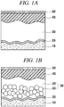
- FIG.1A and FIG.1B are schematic diagrams illustrating a layer structure of a Perovskite solar cell in accordance with an exemplary embodiment of the present disclosure
- FIG. 1C is a SEM image capturing a layer structure of a Perovskite solar cell prepared in accordance with an example of the present disclosure.
- a Perovskite solar cell of the present disclosure may have a sandwich structure in which two electrodes, i.e., a first electrode 10 and a second electrode 20, are in surface contact with each other, but may not be limited thereto.
- the first electrode 10 may be represented as a working electrode or a semiconductor electrode
- the second electrode 50 may be represented as a counter electrode, but may not be limited thereto.
- a recombination-preventing layer 20 is formed on the first electrode, and a photoactive layer 30 is formed on the recombination-preventing layer 20 and may include a layer of a Perovskite represented by the following Chemical Formula 1.
- R includes a +1 cation selected from the group consisting of C n H 2n+1 NH 3 + wherein n is an integer of from 1 to 9, NH 4 + , HC(NH 2 ) 2 + , CS + , NF 4 + , NCl 4 + , PF 4 + , PCl 4 + , CH 3 PH 3 + , CH 3 ASH 3 + , CH 3 SbH 3 + , PH 4 + , ASH 4 + , SbH 4 + , and combinations thereof, M includes a +2 metal cation selected from the group consisting of Pb 2+ , Sn 2+ , Ge 2+ , and combinations thereof, and X is a halogen
- the layer of a Perovskite may include the Perovskite represented by Chemical Formula 1 and formed by reacting MX 2 (herein, M includes a +2 metal cation selected from the group consisting of Pb 2+ , Sn 2+ , Ge 2+ , and combinations thereof and X is a halogen anion) with the precursor for producing a Perovskite including formamidinium halide in accordance with the second aspect of the present disclosure, but may not be limited thereto.
- MX 2 includes a +2 metal cation selected from the group consisting of Pb 2+ , Sn 2+ , Ge 2+ , and combinations thereof and X is a halogen anion
- the precursor for producing a Perovskite including a formamidinium halide may be prepared by reacting, particularly, a formamidinium cation with a metal alkoxide MOR 1 (herein, M is a +2 metal cation and R 1 includes a +1 cation selected from the group consisting of C n H 2n+1 NH 3 + wherein n is an integer of from 1 to 9, NH 4 + , HC(NH 2 ) 2 + , CS + , NF 4 + , NCl 4 + , PF 4 + , PCl 4 + , CH 3 PH 3 + , CH 3 ASH 3 + , CH 3 SbH 3 + , PH 4 + , ASH 4 + , SbH 4 + , and combinations thereof), but may not be limited thereto.
- M is a +2 metal cation and R 1 includes a +1 cation selected from the group consisting of C n H 2n+1 NH 3 + wherein n is an
- the metal alkoxide may include sodium ethoxide, but may not be limited thereto. If a precursor for producing a Perovskite is prepared using the metal alkoxide MOR 1 , it is easy to remove by-products generated during a process for preparing the Perovskite precursor and it is possible to acquire the precursor for producing a Perovskite with a high yield.
- the Perovskite in Chemical Formula 1 may include HC(NH 2 ) 2 MX 3 , but may not be limited thereto.
- the layer of a Perovskite may have a thickness of about 1 ⁇ m or less, but may not be limited thereto.
- the layer of a Perovskite may have a thickness of about 1 ⁇ m or less, about 900 nm or less, about 800 nm or less, about 700 nm or less, about 600 nm or less, about 500 nm or less, about 400 nm or less, about 300 nm or less, about 200 nm or less, or about 100 nm or less, and desirably about 300 nm or less, but may not be limited thereto.
- the layer of a Perovskite may include a layer 35 of Perovskite HC(NH 2 ) 2 MX 3 prepared by reacting MX 2 with a precursor HC(NH 2 ) 2 I prepared by the method in accordance with the first aspect of the present disclosure.
- r R and r M are effective ionic radii of the cations in a cubo-octahedral R-site and an octahedral M-site, respectively, and r X is a radius of the anion.
- CH 3 NH 3 + cation has an ionic radius of 180 pm and thus is suitable for a Perovskite structure.
- a change in the cation may result in a change in Pb-I bond length and/or bond angle, which causes a change in band structure and band gap tuning.
- HC(NH 2 ) 2 PbI 3 absorbs light in a wider range than CH 3 NH 3 Pbl 3 due to its lower band gap, and, thus, it is expected that HC(NH 2 ) 2 PbI 3 has a higher PCE due to a higher photocurrent. Further, a remarkable phase transition in an operation temperature range of a solar cell is not expected. According to a conventional study, it was found that dry crystals ( ⁇ -phase) of black HC(NH 2 ) 2 PbI 3 are converted into ⁇ -phase at about 200 K or less and converted into ⁇ -phase at about 130 K or less.
- HC(NH 2 ) 2 PbI 3 in a Perovskite solar cell showed a low PCE of 4.3% with an unexpectedly very low photocurrent density of 6.45 mA/cm 2 , and in this case, the low photocurrent can be explained as being caused by non-uniformity in conduction band edge between TiO 2 and FAPbI 3 . Since it was confirmed that a scaffold layer including an electron non-injected oxide such as Al 2 O 3 or ZrO 2 is easily operated in a Perovskite solar cell, it may not be a reason for explaining the low photocurrent.
- a hole transport layer (hereinafter, also referred to as "HTM") 40 is formed on the photoactive layer 30, and the second electrode 50 may be formed on the hole transport layer 40.
- the hole transport layer 40 may be formed in order to reduce the oxidized photoactive layer 30, but may not be limited thereto.
- the transparent conductive substrate may include a glass substrate containing a material selected from the group consisting of indium tin oxide (ITO), fluorine tin oxide (FTO), ZnO-Ga 2 O 3 , ZnO-Al 2 O 3 , tin-based oxide, zinc oxide, and combinations thereof or a plastic substrate, but may not be limited thereto.
- the transparent conductive substrate may use any material without particular limitations as long as it has conductance and transparency.
- the plastic substrate may include a member selected from the group consisting of polyethylene terephthalate, polyethylene naphthalate, polycarbonate, polypropylene, polyimide, triacetyl cellulose, and combinations thereof, but may not be limited thereto.
- the photoactive layer 30 may further include a semiconductor layer 33 as an electron transport layer, as illustrated in FIG. 1B , but may not be limited thereto.
- the semiconductor layer 33 is formed on the electron recombination-preventing layer 20
- the Perovskite layer 35 may be formed on the semiconductor layer 33, but may not be limited thereto.
- the semiconductor layer 33 may have a thickness of about 1 ⁇ m or less, but may not be limited thereto.
- the semiconductor layer 33 may have a thickness of about 1 ⁇ m or less, about 900 nm or less, about 800 nm or less, about 700 nm or less, about 600 nm or less, about 500 nm or less, about 400 nm or less, about 300 nm or less, about 200 nm or less, or about 100 nm or less, and desirably about 300 nm or less, but may not be limited thereto.
- the semiconductor layer 33 may have a thickness equal to or smaller than that of the Perovskite layer 35.
- the semiconductor layer 33 may be included in the Perovskite layer 35 as illustrated in FIG. 1B , or the Perovskite infiltrates into pores of the semiconductor layer having a mesoporous structure.
- the semiconductor layer 33 may have a mesoporous structure including pores of from about 20 nm to about 500 nm, but may not be limited thereto.
- the semiconductor layer 33 may include pores of from about 20 nm to about 500 nm, from about 20 nm to about 450 nm, from about 20 nm to about 400 nm, from about 20 nm to about 350 nm, from about 20 nm to about 300 nm, from about 20 nm to about 250 nm, from about 20 nm to about 200 nm, from about 20 nm to about 150 nm, from about 20 nm to about 100 nm, or from about 20 nm to about 50 nm, but may not be limited thereto.
- the pores of the semiconductor layer may be formed using a polymer as a sacrificial material for forming pores.
- the polymer sacrificial material may include a polymer selected from the group consisting of ethylene cellulose, hydroxypropylcellulose, polyethyleneglycol, polyethyleneoxide, polyvinylalcohol, polyvinylpyrrolidone, and combinations thereof, but may not be limited thereto.
- the semiconductor layer may include an organic semiconductor, an inorganic semiconductor, or mixture thereof, but may not be limited thereto.
- the semiconductor layer may include a metal oxide selected from the group consisting of TiO 2 , SnO 2 , ZnO, WO 3 , Nb 2 O 5 , TiSrO 3 , and combinations thereof, but may not be limited thereto.
- the hole transport layer 40 may include a unimolecular or polymeric hole transport material, but may not be limited thereto.
- a unimolecular or polymeric hole transport material such as spiro-MeOTAD [2,2',7,7'-tetrakis(N,N-p-dimethoxy-phenylamino)-9,9'-spirobifluorene] may be used as the unimolecular hole transport material and P3HT[poly(3-hexylthiophene)] may be used as the polymeric hole transport material, but may not be limited thereto.
- the hole transport layer 40 may use a dopant selected from the group consisting of Li-based dopants, Co-based dopants, and combinations thereof, but may not be limited thereto.
- a dopant selected from the group consisting of Li-based dopants, Co-based dopants, and combinations thereof, but may not be limited thereto.
- a mixture of spiro-MeOTAD, tBP, and Li-TFSI may be used as the hole transport material, but the present disclosure may not be limited thereto.
- the second electrode may include a member selected from the group consisting of Pt, Au, Ni, Cu, Ag, In, Ru, Pd, Rh, Ir, Os, C, conductive polymers, and combinations thereof, but may not be limited thereto.
- highly stable gold Au
- Au highly stable gold
- a method of preparing a Perovskite solar cell including: forming a recombination-preventing layer on a first electrode including a transparent conductive substrate; forming a photoactive layer including a Perovskite layer by forming a layer of a Perovskite represented by the following Chemical Formula 1 on the recombination-preventing layer; forming a hole transport layer on the photoactive layer; and forming a second electrode on the hole transport layer: [Chemical Formula 1] RMX 3 , in Chemical Formula 1, R includes a +1 cation selected from the group consisting of C n H 2n+1 NH 3 + wherein n is an integer of from 1 to 9, NH 4 + , HC(NH 2 ) 2 + , CS + , NF 4 + , NCI 4 + , PF 4 + , PCI 4 + , CH 3 PH 3 + , CH 3 ASH 3 + , CH 3 Sb
- the fourth aspect of the present disclosure relates to a method of preparing the Perovskite solar cell in accordance with the third aspect of the present disclosure
- detailed descriptions of the method of preparing the Perovskite solar cell, which overlap with those of the third aspect of the present disclosure, are omitted hereinafter, but the descriptions of the third aspect of the present disclosure may be identically applied to the fourth aspect of the present disclosure, even though they are omitted hereinafter.
- the forming of a photoactive layer may include forming the layer of the Perovskite represented by Chemical Formula 1 formed by reacting MX 2 (herein, M includes a +2 metal cation selected from the group consisting of Pb 2+ , Sn 2+ , Ge 2+ , and combinations thereof and X is a halogen anion) with the precursor for producing a Perovskite including formamidinium halide in accordance with the second aspect of the present disclosure, but may not be limited thereto.
- MX 2 includes a +2 metal cation selected from the group consisting of Pb 2+ , Sn 2+ , Ge 2+ , and combinations thereof and X is a halogen anion
- the photoactive layer may further include a semiconductor layer, but may not be limited thereto.
- the semiconductor layer may have a thickness of about 1 ⁇ m or less, but may not be limited thereto.
- the semiconductor layer may have a thickness of about 1 ⁇ m or less, about 900 nm or less, about 800 nm or less, about 700 nm or less, about 600 nm or less, about 500 nm or less, about 400 nm or less, about 300 nm or less, about 200 nm or less, or about 100 nm or less, and desirably about 300 nm or less, but may not be limited thereto.
- the semiconductor layer may have a mesoporous structure including pores of from about 20 nm to about 500 nm, but may not be limited thereto.
- the semiconductor layer may include pores of from about 20 nm to about 500 nm, from about 20 nm to about 450 nm, from about 20 nm to about 400 nm, from about 20 nm to about 350 nm, from about 20 nm to about 300 nm, from about 20 nm to about 250 nm, from about 20 nm to about 200 nm, from about 20 nm to about 150 nm, from about 20 nm to about 100 nm, or from about 20 nm to about 50 nm, but may not be limited thereto.
- the semiconductor layer may include an organic semiconductor, an inorganic semiconductor, or mixture thereof, but may not be limited thereto.
- the semiconductor layer having the mesoporous structure may be formed by forming and coating a mixture including metal oxide semiconductor nanoparticles and a polymer as a sacrificial material for forming pores and then forming pores by removing the polymer, but may not be limited thereto.
- a pore size of the semiconductor layer may be regulated by regulating a content of the polymer included in the semiconductor layer, but may not be limited thereto.
- the method may further include annealing the photoactive layer at from 100°C to 170°C right after the photoactive layer is formed, but may not be limited thereto.
- the annealing may be performed at from about 100°C to about 170°C, from about 100°C to about 160°C, from about 100°C to about 150°C, from about 100°C to about 140°C, from about 100°C to about 130°C, from about 100°C to about 120°C, from about 100°C to about 110°C, from about 110°C to about 170°C, from about 110°C to about 160°C, from about 110°C to about 150°C, from about 110°C to about 140°C, from about 110°C to about 130°C, from about 110°C to about 120°C, from about 120°C to about 170°C, from about 120°C to about 160°C, from about 120°C to about 150°C, from about 120°C to about 140°C,
- HC(NH 2 ) 2 I was filtered and then dried in a vacuum for 12 hours, so that a precursor HC(NH 2 ) 2 I to form white powder as shown in FIG. 2A .
- the method of synthesizing a precursor HC(NH 2 ) 2 I in accordance with the present Example is different from a conventional method using HI and formamidine acetate in which acetic acid as a by-product is not easily removed from HC(NH 2 ) 2 I. Since the precipitate NaCl in Reaction Formula 2 has a much lower solubility in ethanol, ethanol was used instead of methanol in the present Example (0.65 g NaCI/1 kg of ethanol vs 14 g NaCl/1 kg of methanol).
- the first electrode including the transparent conductive substrate was first produced, and the recombination-preventing layer was formed on the first electrode, and a porous semiconductor/Perovskite complex layer including the porous semiconductor layer and the precursor HC(NH 2 ) 2 I prepared as shown in Reaction Formula 3 was formed on the recombination-preventing layer.
- FTO fluorine-doped tin oxide-coated
- a dense TiO 2 blocking layer (BL) as the recombination-preventing layer was formed by spin-coating a 0.15 M titanium diisopropoxide bis(acetylacetonate (Aldrich, 75 wt.% in isopropanol)/1-butanol (Aldrich, 99.8%) solution and annealing at 500°C for 15 minutes.
- a porous TiO 2 film was deposited on the dense TiO 2 BL by spin-coating TiO 2 paste diluted in ethanol.
- the content of the EC was varied from 0.6 to 1.5 in order to control a pore size and porosity.
- the content of the paste was varied from 0.8 g to 2 g in 10 ml ethanol in order to control the thickness of the film.
- the rate of increase in thickness was about 160 nm/g TriO 2 .
- the TiO 2 paste-coated electrode was annealed at 550°C for 1 hour.
- the electrode was cooled to room temperature and then immersed in a 20 mM TiCl 4 (Aldrich, >98%) aqueous solution at 70°C for 10 minutes and washed with deionized water and then annealed at 500°C for 30.
- a 20 mM TiCl 4 Aldrich, >98%) aqueous solution at 70°C for 10 minutes and washed with deionized water and then annealed at 500°C for 30.
- HC(NH 2 ) 2 PbI 3 having a thickness of 300 nm was formed on the porous TiO 2 film by a two-step method using the formamidinium iodide and PbI 2 available in the market.
- the PbI 2 -coated TiO 2 film was dried at 40°C for 3 minutes and at 100°C for 10 minutes.
- HC(NH 2 ) 2 PbI 3 the PbI 2 -coated TiO 2 film was immersed for 1 minute in a 0.01 g/mL HC(NH 2 ) 2 I solution in 2-propanol (Sigma-Aldrich, 99.5%) and rotated at 500 rpm for 5 seconds, at 1,500 rpm for 10 seconds, and at 3,000 rpm for 20 seconds, and then dried at 40°C for 3 minutes and at 150 °C for 15 minutes.
- the film was immersed for 15 minutes and washed with the 2-propanol solution and then dried at 150°C for 5 minutes.
- a solution for spiro-MeOTAD coating was prepared by dissolving 72.3 mg spiroMeOTAD in 1 mL chlorobenzene, and 28.8 ⁇ L 4-tert-butyl pyridine and 17.5 ⁇ L lithium bis(trifluoromethanesulfonyl)imide] solution [520 mg Li-TFSI in 1 mL acetonitrile (Sigma-Aldrich, 99.8%)] were added thereto.
- the spiro-MeOTAD was deposited at 4,000 rpm for 20 seconds.
- a precursor HC(NH 2 ) 2 I was prepared using HC(NH)(NH 2 ), HCl and methanol as shown in the following Formula 4: HC(NH)(NH 2 ). HCl + NaOCH 3 ⁇ HC(NH)(NH 2 ) + NaCl ( ⁇ ) + CH 3 OH (4).
- HC(NH)(NH 2 ) 2 I in the form of yellow powder as shown in FIG. 2B was prepared with a yield of from 10% to 20%.
- a precursor HC(NH 2 ) 2 I in the form of white powder as shown in FIG. 2C was prepared with a yield of 80% using HC(NH)(NH 2 ), HI, and acetic acid as shown in the following Formula 5.
- a Perovskite solar cell was prepared in the same manner as Example using the HC(NH 2 ) 2 I prepared according to the synthesis method of Comparative Example 2.
- HRMS high resolution mass spectroscopy
- HC(NH 2 ) 2 PbI 3 film was used on a dense TiO 2 -coated FTO glass.
- the transmission and the reflectance were measured by a UV-vis spectrophotometer (Perkin Elmer, lamda 35) using an integrating sphere and a dense TiO 2 -coated FTO glass as a blank for measurement of transmittance.
- X-ray diffraction patterns were collected by a Bruker AXS (D8 advance, Bruker Corporation) using Cu Ka radiation at a scan rate of 4°/min.
- Morphology of surface and cross section was obtained by a scanning electron microscope (SEM, JSM-7600F, JEOL).
- a current and a voltage were measured using a Keithley 2400 source meter under one sun illumination (AM 1.5G, 100 mW/cm 2 ) and simulated by a solar simulator (Oriel Sol3A class AAA) equipped with a 450 W Xenon lamp (Newport 6279NS).
- the intensity of light was regulated by a NREL-calibrated Si solar cell equipped with a KG-2 filter.
- the device was covered with a metal aperture mask.
- IPCE photon-to-electron conversion efficiency
- a monochromatic beam was generated from a 75 W Xenon lamp (USHIO, Japan).
- IPCE data were collected in a DC mode without bias light.
- Time-limited photocurrent response was monitored using a 550 nm monochromatic beam at 4 Hz.
- a broad NH 2 peak and a sharp CH peak were observed around 8.5 and 7.8 as shown in FIG. 3 , and the other peaks were dimethylsulfoxide (hereinafter, also referred to as "DMSO") used as a solvent for the NMR measurement and water present in the solvent.
- DMSO dimethylsulfoxide
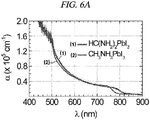
- the absorption coefficient of a 250 nm-HC(NH 2 ) 2 PbI 3 (hereinafter, also referred to as "FAPbI 3 ”) film prepared in accordance with the present Example was 1.53 ⁇ 10 5 cm -1 at 500 nm, 0.53 ⁇ 10 5 cm -1 at 600 nm, and 0.30 x 10 5 cm -1 at 700 nm ( FIG. 6A ), and measured using a formula reported in other studies.
- the absorption coefficient of the FAPbI 3 at a given wavelength was slightly higher than that of CH 3 NH 3 Pbl 3 (hereinafter, also referred to as "MAPbI 3 ”) which has been conventionally studied.
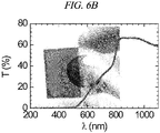
- a FAPbI 3 -coated 200 nm-TiO 2 film (total thickness: about 300 nm) was transparent brown as shown in FIG. 6B .
- An increase in transmittance from 600 nm to 840 nm implies loss of light reflection at a long wavelength.
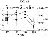
- a photocurrent-voltage characteristic depending on a heat treatment temperature for the porous semiconductor/Perovskite complex layer of the Perovskite solar cell including the precursor HC(NH 2 ) 2 I prepared in accordance with the present Example and an external quantum efficiency corresponding to each device were measured.
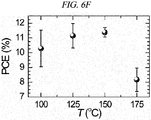
- Table 3 shows photocurrent density (J SC ), photovoltage (V OC ), fill factor (FF), and photo-to-electron conversion efficiency of the Perovskite HC(NH 2 ) 2 PbI 3 solar cell depending on a heat treatment temperature. The efficiency was observed to be highest in case of performing a heat treatment at 150°C, which was considered as being caused by a high current density resulting from a high quantum conversion efficiency.
- the PCE is increased along an increase in annealing temperature from 100°C to 150°C and then sharply decreased at 175°C.
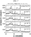
- the measurement of X-ray diffraction was conducted in order to find out the basis for strong dependence of the photovoltaic performance on an annealing temperature.
- FIG. 7A through FIG. 7E XRD reflection at 24.26°, 28.04°, 31.42°, 40.1°, and 42.7° was indexed to (202), (220), (222), (400), and (330) reflections each corresponding to a black FAPbI 3 polymorph.
- the intensity of the (202) reflection was almost similar to those of the (202) and (222) reflections, which shows that preferred orientation of the FAPbI 3 layer of the present disclosure is different from the reported result.
- Decomposition of the FAPbI 3 was not observed in the temperature range of from 100°C to 175°C, which is connected to no heat transfer in the above-described temperature range measured using a differential scanning calorimeter (DSC) (of which data are not illustrated).
- DSC differential scanning calorimeter
- the deterioration of performance in a long time-heat treatment at 150°C is connected to partial decomposition of the FAPbI 3 as indicated by a negative heat flow in a DSC analysis ( FIG. 8F ).
- a heating condition for DSC measurement is not exactly identical to that for preparation of a Perovskite sample, but it is clear that crystallization is completed within 15 minutes.
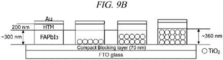
- FAPbI 3 having a thickness of about 300 nm was formed on a dense wall layer, and FAPbI 3 was formed to a similar thickness on 130 nm- and 230 nm-porous TiO 2 films, but FAPbI 3 was formed to a slightly increased thickness on a 320 nm-TiO 2 film.
- the pores of the porous TiO 2 films were entirely filled with FAPbI 3 , and upper parts of the deposited FAPbI 3 layers appear flat.
- FIG. 9B schematically illustrates structures of the layers.
- FIG. 9C The presence and absence of a porous TiO 2 film and a thickness of the TiO 2 film considerably affect a charge collection rate ( FIG. 9C ), photovoltaic performance ( FIG. 9D ), shunt, and series resistances ( FIG. 9E ).
- a time-limited photocurrent signal was detected under 550 nm-monochromatic beam.
- the device signal amplitude was increased with an increase in thickness of a TiO 2 film, along with a fast collection rate.
- the presence of a porous TiO 2 film is important in facilitating photocurrent collection.
- J SC was significantly improved from about 13 mA/cm 2 to about 19 mA/cm 2 by introduction of the porous TiO 2 film.
- V OC was also improved from 948 mV to 1,015 mV, but slightly decreased to 971 mV in the 320 nm-TiO 2 film.
- V OC in the 320 nm-TiO 2 film may be probably connected to recombination caused by the increased FAPbI 3 layer.
- FF is increased when a porous TiO 2 film is included and as its thickness is increased.
- a series resistance is decreased by more than one order of magnitude and a shunt resistance is increased by 4.6 times ( FIG. 9E ), which results from the improved fill factor.
- a high series resistance and a low shunt resistance in a FAPbI 3 layer without a porous TiO 2 film indicates the presence of a resistance-related component.
- porous TiO 2 layer The function of the porous TiO 2 layer is clear as demonstrated by a gradual increase of shunt resistance along with an increase of a TiO 2 layer.
- IPCE IPCE Detection of IPCE is also affected by the presence and thickness of a TiO 2 film.
- IPCE signal by including and increasing a porous TiO 2 layer indirectly proves injection of electrons into a TiO 2 layer, which can be explained partially as a basis for resistance change.
- the presence of a porous TiO 2 layer is advantageous as compared with a planar structure in terms of resistance control and charge collection.
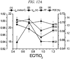
- a mixed porous TiO 2 nanostructure including small and large pores by means of variation of content of polymer vehicle ethyl cellulose (EC) in TiO 2 paste was designed.
- microporous structure formed by high EC content is expected to induce large FAPbI 3 crystals, which is likely to reduce the number of grain boundaries relating to resistance components.
- Too much EC content is not recommended because of the loss of V OC .
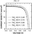
- FIG. 13 shows a current-voltage characteristic depending on a r composition ratio of a polymer in TiO 2 nanoparticle paste used for forming the porous TiO 2 nanoparticle layer, and it could be seen that when a ratio of the TiO 2 nanoparticles : polymer (ethyl cellulose) was 1:0.72, the highest efficiency was obtained, and also it could be seen that a fill factor (FF) was improved depending on a composition ratio of the polymer.
- FF fill factor
- Table 4 shows photocurrent density (J SC ), photovoltage (V OC ), fill factor (FF), and photo-to-electron conversion efficiency depending on a ratio of the polymer in the TiO 2 nanoparticle paste in preparing a HC(NH 2 ) 2 PbI 3 Perovskite solar cell.
- FIG. 12C and FIG. 12D are electron microscopic cross-sectional images depending on a composition ratio of a polymer in TiO 2 nanoparticle paste used for forming a porous TiO 2 nanoparticle layer, and it could be seen that as a composition ratio of the polymer was increased, an interface between a Perovskite layer and a hole transport layer was increased, which may contribute to the improvement in FF as shown in FIG. 6C and FIG. 6D .
- FIG. 14 shows a photocurrent-voltage graph for a HC(NH 2 ) 2 PbI 3 solar cell prepared using the most optimum conditions found through experiments, and photocurrent density (J SC ), photovoltage (V OC ), fill factor (FF), and photo-to-electron conversion efficiency of the HC(NH 2 ) 2 PbI 3 solar cell prepared in these conditions were measured 6 times, and the results thereof were as listed in the following Table 5.
- HC(NH 2 ) 2 PbI 3 methylammonium lead iodide HC(NH 2 ) 2 PbI 3 -based high-efficiency, J-V hysteresis-free and photo-stable Perovskite solar cell was successfully prepared.
- HC(NH 2 ) 2 PbI 3 was prepared by immersing PbI 2 -coated electrode in HC(NH 2 ) 2 I solution. It was found that the annealing temperature and time for the deposited HC(NH 2 ) 2 PbI 3 is very important for photovoltaic performance. A black HC(NH 2 ) 2 PbI 3 polymorph formed at 150°C for 15 minutes showed the highest photocurrent. It was also found that a porous TiO 2 layer is important for improvement in other parameters such as charge collection, fill factor, and voltage. A high fill factor was realized by engineering a porous structure of the TiO 2 layer via EC/TiO 2 ratio control.
Landscapes
- Chemical & Material Sciences (AREA)
- Organic Chemistry (AREA)
- Engineering & Computer Science (AREA)
- Materials Engineering (AREA)
- Life Sciences & Earth Sciences (AREA)
- Geology (AREA)
- Inorganic Chemistry (AREA)
- Photovoltaic Devices (AREA)
- Environmental & Geological Engineering (AREA)
- General Life Sciences & Earth Sciences (AREA)
- Manufacturing & Machinery (AREA)
Abstract
Description
- The invention relates to a precursor for producing a Perovskite, a method of preparing the precursor, a solar cell including the Perovskite prepared by using the precursor for producing a Perovskite, and a method of preparing the solar cell.
- A organic-inorganic hybrid Perovskite was first applied to a solar cell by Tsutomu Miyasaka's group in 2009 in Japan [J. Am. Chem. Soc. 2009, 131, 6050-6051], and has recently attracted a lot of attention as a light absorbing material for a solar cell due to its high absorption coefficient and property that can be easily synthesized through a solution process.
- After the present research team first published a solid hole conductor-based Perovskite solar cell with a photovoltaic conversion efficiency of 9.7% in 2012 [Sci. Rep. 2012, 2:579, 1-7], numerous follow-up studies have been conducted.
- Most of Perovskite photoactive layers researched so far are CH3NH3Pbl3 and CH3NH3Pbl3-xClx.
- The excellent photovoltaic performance of such a methylammonium lead halide Perovskite is derived from its long-range charge transport property and high light absorbing property. The absorption coefficient of CH3NH3Pbl3 is about one order of magnitude higher than those of molecular sensitizers such as ruthenium bipyridyl complex. Further, CH3NH3Pbl3 and CH3NH3Pbl3-xClx can transport electrons and holes when CH3NH3Pbl3 has diffusion lengths of about 130 nm for an electron and about 100 nm for a hole and CH3NH3PbI3-xClx has diffusion lengths of about 1,069 nm for an electron and about 1,213 nm for a hole.
- The balanced electron and hole transport properties of CH3NH3PbX3 (X=I or I-Cl) form a Perovskite which is a solar cell with a planar heterojunction structure.
- Charge accumulation capability of CH3NH3Pbl3 Perovskite has been reported, and supports generation of free charge carriers and a resultant high open circuit voltage close to about 1.1 V.
- Triiodide and the mixed methylammonium lead halide Perovskites are stabilized in a tetragonal phase at room temperature, which have a band gap of about 1.5 eV.
- Assuming that there is no loss of incident light caused by reflection from a transparent conductive substrate, a maximum photocurrent density is theoretically about 27.2 mA/cm2 and an absorption onset wavelength measured from an incident photovoltaic conversion efficiency (IPCE) is about 800 nm. However, it is necessary to consider the occurrence of light loss of from about 15% to about 20% in an actual apparatus, and in this case the photocurrent density is from about 23.1 mA/cm2 to about 21.8 mA/cm2. Therefore, a methylammonium lead halide-based Perovskite cell may have a PCE of about 20% when a voltage of about 1.1 V and a fill factor of about 0.8 are satisfied.
- However, the methylammonium cation-based organic-inorganic hybrid Perovskite has a band gap of about 1.55 eV and can absorb a light having a wavelength of up to about 800 nm, and thus production amount of photocurrent is limited to about 21 mA/cm2. Further, for a conventional methylammonium cation-based organic-inorganic hybrid Perovskite solar cell, hysteresis is caused by an external voltage, and, thus, it is difficult to precisely measure photovoltaic properties. Furthermore, the conventional methylammonium cation-based organic-inorganic hybrid Perovskite solar cell undergoes a reversible phase transition between tetragonal and cubic symmetry at a temperature between about 300 K and about 400 K corresponding to an operation temperature of the solar cell, and such a structural phase transition is expected to involve a change of a band structure and may affect the photovoltaic properties.
- Therefore, a Perovskite which is not affected by a phase transition is demanded. Further, a Perovskite with a low band gap is demanded to further improve a PCE.
- A formamidinium cation-based Perovskite was reported as an alternative material to the conventional methylammonium cation-based organic-inorganic hybrid Perovskite solar cell having the above-described problems [Inorg. Chem. 2013, 52, 9019-9038].
- However, when the formamidinium cation-based Perovskite is actually applied to a solar cell, it was reported that the maximum efficiency was about 14.2% and an average efficiency was about 9% using a p-i-n junction structure [Energy Environ. Sci., 2014, 7, p982-988].
- Accordingly, the present disclosure provides a precursor for producing a Perovskite, a method of preparing the precursor, a solar cell including the Perovskite prepared by using the precursor for producing a Perovskite, and a method of preparing the solar cell.
- However, problems to be solved by the present disclosure are not limited to the above-described problems, and although not described herein, other problems to be solved by the present disclosure can be clearly understood by those skilled in the art from the following descriptions.
- In accordance with a first aspect of the present disclosure, there is provided a method of preparing a precursor for producing a Perovskite, including: reacting a formamidine·HX wherein X is a halide with a metal alkoxide to obtain a formamidine; and reacting the obtained formamidine with HX wherein X is a halide to obtain a formamidinium halide.
- In accordance with a second aspect of the present disclosure, there is provided a precursor for producing a Perovskite, including a formamidinium halide prepared by the method in accordance with the first aspect of the present disclosure.
- In accordance with a third aspect of the present disclosure, there is provided a Perovskite solar cell, including: a first electrode including a transparent conductive substrate; a recombination-preventing layer formed on the first electrode; a photoactive layer formed on the recombination-preventing layer; a hole transport layer formed on the photoactive layer; and a second electrode formed on the hole transport layer, wherein the photoactive layer includes a layer of Perovskite including a Perovskite represented by the following Chemical Formula 1:
[Chemical Formula 1] RMX3,
inChemical Formula 1, R includes a +1 cation selected from the group consisting of CnH2n+1NH3 + wherein n is an integer of from 1 to 9, NH4 +, HC(NH2)2 +, CS+, NF4 +, NCl4 +, PF4 +, PCl4 +, CH3PH3 +, CH3ASH3 +, CH3SbH3 +, PH4 +, ASH4 +, SbH4 +, and combinations thereof, M includes a +2 metal cation selected from the group consisting of Pb2+, Sn2+, Ge2+, and combinations thereof, and X is a halogen anion. - In accordance with a fourth aspect of the present disclosure, there is provided a method of preparing a Perovskite solar cell, including: forming a recombination-preventing layer on a first electrode including a transparent conductive substrate; forming a photoactive layer including a Perovskite layer by forming a layer of a Perovskite represented by the following Chemical Formula 1 on the recombination-preventing layer; forming a hole transport layer on the photoactive layer; and forming a second electrode on the hole transport layer:
[Chemical Formula 1] RMX3,
inChemical Formula 1, R includes a +1 cation selected from the group consisting of CnH2n+1NH3 + wherein n is an integer of from 1 to 9, NH4 +, HC(NH2)2 +, CS+, NF4 +, NCl4 +, PF4 +, PCl4 +, CH3PH3 +, CH3ASH3 +, CH3SbH3 +, PH4 +, ASH4 +, SbH4 +, and combinations thereof, M includes a +2 metal cation selected from the group consisting of Pb2+, Sn2+, Ge2+, and combinations thereof, and X is a halogen anion. - According to an exemplary embodiment of the present disclosure, a light absorption wavelength region of a Perovskite light-absorbing material can be increased to about 850 nm which is wider by about 50 nm than that of a conventional methylammonium cation-based Perovskite light-absorbing material having a light absorption wavelength region of about 800 nm, by using a formamidinium cation-based Perovskite having a band gap energy of about 1.45 eV reduced by about 0.1 eV as compared with the conventional methylammonium cation-based Perovskite.
- According to an exemplary embodiment of the present disclosure, when preparing a precursor for producing a Perovskite, a formamidinium cation and a metal alkoxide including an alkali metal are used, and, thus, it is easy to remove by-products and the precursor for producing a Perovskite can be prepared with a high yield of about 90% or more, as compared with a conventional precursor for producing a Perovskite. In particular, if sodium ethoxide is used as the metal alkoxide, it is easy to remove by-products, i.e., NaX (e.g., NaCl), C2H5OH, and the like after the reaction and thus the yield of the precursor can be improved.
- According to an exemplary embodiment of the present disclosure, the efficiency of a solar cell is generally determined by multiplying a photocurrent, a photovoltage, and a fill factor, and since the amount of photocurrent is increased according to an exemplary embodiment of the present disclosure, improvement in final efficiency of a solar cell can be expected.
- Further, according to an exemplary embodiment of the present disclosure, the occurrence of hysteresis caused by an external voltage is decreased as compared with a conventional methylammonium cation-based Perovskite solar cell, and, thus, it is possible to easily measure photovoltaic properties.
-
-
FIG. 1A to FIG. 1C illustrate a structure of a Perovskite solar cell in accordance with an exemplary embodiment of the present disclosure. -
FIG. 2A to FIG. 2C are images of precursor powder for Perovskite solar cell obtained in accordance with an example of the present disclosure. -
FIG. 3 is a H NMR spectrum of a precursor for solar cell prepared by a synthesis method in accordance with an example of the present disclosure. -
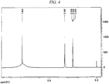
FIG. 4 is a H NMR spectrum of a precursor for solar cell prepared by a synthesis method in accordance with Comparative Example 1 of the present disclosure. -
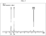
FIG. 5 is a H NMR spectrum of a precursor for solar cell prepared by a synthesis method in accordance with Comparative Example 2 of the present disclosure. -
FIG. 6A to FIG. 6F show light absorption properties of a Perovskite solar cell in accordance with an example of the present disclosure. -
FIG. 7A to FIG. 7E show X-ray diffraction patterns depending on a temperature in accordance with an example of the present disclosure. -
FIG. 8A to FIG. 8F show photovoltaic effects depending on an annealing duration at about 150°C in accordance with an example of the present disclosure. -
FIG. 9A to FIG. 9E show photovoltaic effects depending on a thickness of a TiO2-containing semiconductor layer in accordance with an example of the present disclosure. -
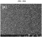
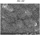
FIG. 10A to FIG. 10F are SEM images showing an upper part of a photoactive layer formed on a TiO2-containing semiconductor layer in accordance with an example of the present disclosure. -
FIG. 11A and FIG. 11B show the dependence of IPCE depending on a thickness of a TiO2-containing semiconductor layer in accordance with an example of the present disclosure. -
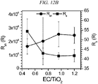
FIG.12A to FIG. 12F show effects depending on a content of a polymer present in TiO2 paste in accordance with an example of the present disclosure. -
FIG. 13 shows an effect depending on a content of a polymer present in TiO2 paste in accordance with an example of the present disclosure. -
FIG. 14 shows a photocurrent-voltage curve of a solar cell including HC(NH2)2PbI3 Perovskite in accordance with an example of the present disclosure. - Hereinafter, embodiments and examples of the present disclosure will be described in detail with reference to the accompanying drawings so that the present disclosure may be readily implemented by those skilled in the art. However, it is to be noted that the present disclosure is not limited to the embodiments and examples but can be embodied in various other ways. In drawings, parts irrelevant to the description are omitted for the simplicity of explanation, and like reference numerals denote like parts through the whole document.
- Through the whole document, the term "connected to" or "coupled to" that is used to designate a connection or coupling of one element to another element includes both a case that an element is "directly connected or coupled to" another element and a case that an element is "electronically connected or coupled to" another element via still another element.
- Through the whole document, the term "on" that is used to designate a position of one element with respect to another element includes both a case that the one element is adjacent to the another element and a case that any other element exists between these two elements.
- Further, through the whole document, the term "comprises or includes" and/or "comprising or including" used in the document means that one or more other components, steps, operation and/or existence or addition of elements are not excluded in addition to the described components, steps, operation and/or elements unless context dictates otherwise. Through the whole document, the term "about or approximately° or "substantially" are intended to have meanings close to numerical values or ranges specified with an allowable error and intended to prevent accurate or absolute numerical values disclosed for understanding of the present disclosure from being illegally or unfairly used by any unconscionable third party. Through the whole document, the term "step of" does not mean "step for".
- Through the whole document, the term "combination of" included in Markush type description means mixture or combination of one or more components, steps, operations and/or elements selected from a group consisting of components, steps, operation and/or elements described in Markush type and thereby means that the disclosure includes one or more components, steps, operations and/or elements selected from the Markush group.
- Through the whole document, a phrase in the form "A and/or B" means "A or B, or A and B".
- Through the whole document, a "Perovskite" has an ABX3 structure, and the ABX3 structure can be readily estimated based on a tolerance factor t:

- Herein, rA and rB are effective ionic radiuses of cations in a cubo-octahedral A-site and an octahedral B-site, respectively, and rx is a radius of an anion.
- Hereinafter, exemplary embodiments and examples of the present disclosure will be described in detail with reference to the accompanying drawings. However, the present disclosure may not be limited to the exemplary embodiment, examples, and drawings.
- In accordance with a first aspect of the present disclosure, there is provided a method of preparing a precursor for producing a Perovskite, including: reacting a formamidine·HX wherein X is a halide with a metal alkoxide to obtain a formamidine; and reacting the obtained formamidine with HX wherein X is a halide to obtain a a formamidinium halide.
- In accordance with an exemplary embodiment of the present disclosure, the metal alkoxide may include MOR1, wherein M is a +2 alkali metal cation and R1 includes a +1 cation selected from the group consisting of CnH2n+1NH3 + wherein n is an integer of from 1 to 9, NH4 +, HC(NH2)2 +, CS+, NF4 +, NCl4 +, PF4 +, PCl4 +, CH3PH3 +, CH3ASH3 +, CH3SbH3 +, PH4 +, ASH4 +, SbH4 +, and combinations thereof.
- In accordance with an exemplary embodiment of the present disclosure, R1 may include a linear or branched, saturated or unsaturated alkyl group having 1 to 20 carbon atoms, and may include, for example, methyl, ethyl, propyl, butyl, pentyl, hexyl, heptyl, octyl, nonyl, decyl, or all available isomers thereof, but may not be limited thereto.
- In accordance with an exemplary embodiment of the present disclosure, the metal alkoxide may include an alkali metal alkoxide, but may not be limited thereto. For example, the metal alkoxide may include sodium ethoxide, but may not be limited thereto. In accordance with an exemplary embodiment of the present disclosure, if a precursor for producing a Perovskite is prepared using a metal alkoxide, it is easy to remove by-products generated during a process for preparing the Perovskite precursor and it is possible to obtain the precursor for producing a Perovskite with a high yield.
- In accordance with an exemplary embodiment of the present disclosure, the HX may include a member selected from the group consisting of HI, HCl, HBr, and combinations thereof, but may not be limited thereto.
- In accordance with an exemplary embodiment of the present disclosure, the formamidinium halide may include a member selected from the group consisting of formamidinium iodide, formamidinium chloride, formamidinium bromide, and combinations thereof, but may not be limited thereto.
- A solar cell may be prepared using a Perovskite prepared using the precursor for producing a Perovskite acquired by the method in accordance with the first aspect of the present disclosure, and, thus, it is possible to prepare a Perovskite solar cell with an excellent photovoltaic efficiency.
- In accordance with a second aspect of the present disclosure, there is provided a precursor for producing a Perovskite including a formamidinium halide prepared by the method in accordance with the first aspect of the present disclosure.
- In accordance with an exemplary embodiment of the present disclosure, the formamidinium halide may include an alkali metal, but may not be limited thereto.
- In accordance with a third aspect of the present disclosure, there is provided a Perovskite solar cell including: a first electrode including a transparent conductive substrate; a recombination-preventing layer formed on the first electrode; a photoactive layer formed on the recombination-preventing layer; a hole transport layer formed on the photoactive layer; and a second electrode formed on the hole transport layer, and the photoactive layer includes a Perovskite layer including a Perovskite represented by the following Chemical Formula 1:
[Chemical Formula 1] RMX3,
inChemical Formula 1, R includes a +1 cation selected from the group consisting of CnH2n+1NH3 + wherein n is an integer of from 1 to 9, NH4 +, HC(NH2)2 +, CS+, NF4 +, NCl4 +, PF4 +, PCl4 +, CH3PH3 +, CH3ASH3 +, CH3SbH3 +, PH4 +, ASH4 +, SbH4 +, and combinations thereof, M includes a +2 metal cation selected from the group consisting of Pb2+, Sn2+, Ge2+, and combinations thereof, and X is a halogen anion. - In accordance with an exemplary embodiment of the present disclosure, in
Chemical Formula 1, R may include a linear or branched, saturated or unsaturated alkyl group having 1 to 20 carbon atoms, and may include, for example, methyl, ethyl, propyl, butyl, pentyl, hexyl, heptyl, octyl, nonyl, decyl, or all available isomers thereof, but may not be limited thereto. - In this regard,
FIG.1A and FIG.1B are schematic diagrams illustrating a layer structure of a Perovskite solar cell in accordance with an exemplary embodiment of the present disclosure, andFIG. 1C is a SEM image capturing a layer structure of a Perovskite solar cell prepared in accordance with an example of the present disclosure. - Referring to
FIG. 1A , a Perovskite solar cell of the present disclosure may have a sandwich structure in which two electrodes, i.e., afirst electrode 10 and asecond electrode 20, are in surface contact with each other, but may not be limited thereto. For example, thefirst electrode 10 may be represented as a working electrode or a semiconductor electrode, and thesecond electrode 50 may be represented as a counter electrode, but may not be limited thereto. - A recombination-preventing
layer 20 is formed on the first electrode, and aphotoactive layer 30 is formed on the recombination-preventinglayer 20 and may include a layer of a Perovskite represented by the followingChemical Formula 1.
[Chemical Formula 1] RMX3,
inChemical Formula 1, R includes a +1 cation selected from the group consisting of CnH2n+1NH3 + wherein n is an integer of from 1 to 9, NH4 +, HC(NH2)2 +, CS+, NF4 +, NCl4 +, PF4 +, PCl4 +, CH3PH3 +, CH3ASH3 +, CH3SbH3 +, PH4 +, ASH4 +, SbH4 +, and combinations thereof, M includes a +2 metal cation selected from the group consisting of Pb2+, Sn2+, Ge2+, and combinations thereof, and X is a halogen anion. - In accordance with an exemplary embodiment of the present disclosure, the layer of a Perovskite may include the Perovskite represented by
Chemical Formula 1 and formed by reacting MX2 (herein, M includes a +2 metal cation selected from the group consisting of Pb2+, Sn2+, Ge2+, and combinations thereof and X is a halogen anion) with the precursor for producing a Perovskite including formamidinium halide in accordance with the second aspect of the present disclosure, but may not be limited thereto. The precursor for producing a Perovskite including a formamidinium halide may be prepared by reacting, particularly, a formamidinium cation with a metal alkoxide MOR1 (herein, M is a +2 metal cation and R1 includes a +1 cation selected from the group consisting of CnH2n+1NH3 + wherein n is an integer of from 1 to 9, NH4 +, HC(NH2)2 +, CS+, NF4 +, NCl4 +, PF4 +, PCl4 +, CH3PH3 +, CH3ASH3 +, CH3SbH3 +, PH4 +, ASH4 +, SbH4 +, and combinations thereof), but may not be limited thereto. For example, the metal alkoxide may include sodium ethoxide, but may not be limited thereto. If a precursor for producing a Perovskite is prepared using the metal alkoxide MOR1, it is easy to remove by-products generated during a process for preparing the Perovskite precursor and it is possible to acquire the precursor for producing a Perovskite with a high yield. - In accordance with an exemplary embodiment of the present disclosure, the Perovskite in
Chemical Formula 1 may include HC(NH2)2MX3, but may not be limited thereto. - In accordance with an exemplary embodiment of the present disclosure, the layer of a Perovskite may have a thickness of about 1 µm or less, but may not be limited thereto. For example, the layer of a Perovskite may have a thickness of about 1 µm or less, about 900 nm or less, about 800 nm or less, about 700 nm or less, about 600 nm or less, about 500 nm or less, about 400 nm or less, about 300 nm or less, about 200 nm or less, or about 100 nm or less, and desirably about 300 nm or less, but may not be limited thereto.
- In accordance with an exemplary embodiment of the present disclosure, the layer of a Perovskite may include a
layer 35 of Perovskite HC(NH2)2MX3 prepared by reacting MX2 with a precursor HC(NH2)2I prepared by the method in accordance with the first aspect of the present disclosure. - In accordance with an exemplary embodiment of the present disclosure, the Perovskite RMX3 structure can be readily estimated based on a tolerance factor t: t = (rR + rX)/[21/2(rM + rx)]. Herein, rR and rM are effective ionic radii of the cations in a cubo-octahedral R-site and an octahedral M-site, respectively, and rX is a radius of the anion. A radius of the cation from RPbI3 was calculated in the range of from 164 pm for t = 0.8 to 259 pm for t = 1 based on Pb2+ = 119 pm and I- = 220 pm. For example, CH3NH3 + cation has an ionic radius of 180 pm and thus is suitable for a Perovskite structure. A change in the cation may result in a change in Pb-I bond length and/or bond angle, which causes a change in band structure and band gap tuning. Substitution by slightly larger formamidinium [HC(NH2)2 +] for methylammonium (CH3NH3 +) can be stabilized as a trigonal Perovskite structure (black) or a hexagonal non-Perovskite structure (yellow). A band gap of HC(NH2)2PbI3 was estimated at 1.45 eV which is lower than that(1.52 eV) of CH3NH3Pbl3 due to the lowered symmetry. Therefore, it is expected that HC(NH2)2PbI3 absorbs light in a wider range than CH3NH3Pbl3 due to its lower band gap, and, thus, it is expected that HC(NH2)2PbI3 has a higher PCE due to a higher photocurrent. Further, a remarkable phase transition in an operation temperature range of a solar cell is not expected. According to a conventional study, it was found that dry crystals (α-phase) of black HC(NH2)2PbI3 are converted into β-phase at about 200 K or less and converted into γ-phase at about 130 K or less. However, HC(NH2)2PbI3 in a Perovskite solar cell showed a low PCE of 4.3% with an unexpectedly very low photocurrent density of 6.45 mA/cm2, and in this case, the low photocurrent can be explained as being caused by non-uniformity in conduction band edge between TiO2 and FAPbI3. Since it was confirmed that a scaffold layer including an electron non-injected oxide such as Al2O3 or ZrO2 is easily operated in a Perovskite solar cell, it may not be a reason for explaining the low photocurrent.
- A hole transport layer (hereinafter, also referred to as "HTM") 40 is formed on the
photoactive layer 30, and thesecond electrode 50 may be formed on thehole transport layer 40. Thehole transport layer 40 may be formed in order to reduce the oxidizedphotoactive layer 30, but may not be limited thereto. - In accordance with an exemplary embodiment of the present disclosure, the transparent conductive substrate may include a glass substrate containing a material selected from the group consisting of indium tin oxide (ITO), fluorine tin oxide (FTO), ZnO-Ga2O3, ZnO-Al2O3, tin-based oxide, zinc oxide, and combinations thereof or a plastic substrate, but may not be limited thereto. The transparent conductive substrate may use any material without particular limitations as long as it has conductance and transparency. For example, the plastic substrate may include a member selected from the group consisting of polyethylene terephthalate, polyethylene naphthalate, polycarbonate, polypropylene, polyimide, triacetyl cellulose, and combinations thereof, but may not be limited thereto.
- In accordance with an exemplary embodiment of the present disclosure, the
photoactive layer 30 may further include asemiconductor layer 33 as an electron transport layer, as illustrated inFIG. 1B , but may not be limited thereto. For example, after thesemiconductor layer 33 is formed on the electron recombination-preventinglayer 20, thePerovskite layer 35 may be formed on thesemiconductor layer 33, but may not be limited thereto. - In accordance with an exemplary embodiment of the present disclosure, the
semiconductor layer 33 may have a thickness of about 1 µm or less, but may not be limited thereto. For example, thesemiconductor layer 33 may have a thickness of about 1 µm or less, about 900 nm or less, about 800 nm or less, about 700 nm or less, about 600 nm or less, about 500 nm or less, about 400 nm or less, about 300 nm or less, about 200 nm or less, or about 100 nm or less, and desirably about 300 nm or less, but may not be limited thereto. In accordance with an exemplary embodiment of the present disclosure, thesemiconductor layer 33 may have a thickness equal to or smaller than that of thePerovskite layer 35. For example, thesemiconductor layer 33 may be included in thePerovskite layer 35 as illustrated inFIG. 1B , or the Perovskite infiltrates into pores of the semiconductor layer having a mesoporous structure. - In accordance with an exemplary embodiment of the present disclosure, the
semiconductor layer 33 may have a mesoporous structure including pores of from about 20 nm to about 500 nm, but may not be limited thereto. For example, thesemiconductor layer 33 may include pores of from about 20 nm to about 500 nm, from about 20 nm to about 450 nm, from about 20 nm to about 400 nm, from about 20 nm to about 350 nm, from about 20 nm to about 300 nm, from about 20 nm to about 250 nm, from about 20 nm to about 200 nm, from about 20 nm to about 150 nm, from about 20 nm to about 100 nm, or from about 20 nm to about 50 nm, but may not be limited thereto. For example, the pores of the semiconductor layer may be formed using a polymer as a sacrificial material for forming pores. The polymer sacrificial material may include a polymer selected from the group consisting of ethylene cellulose, hydroxypropylcellulose, polyethyleneglycol, polyethyleneoxide, polyvinylalcohol, polyvinylpyrrolidone, and combinations thereof, but may not be limited thereto. - In accordance with an exemplary embodiment of the present disclosure, the semiconductor layer may include an organic semiconductor, an inorganic semiconductor, or mixture thereof, but may not be limited thereto.
- In accordance with an exemplary embodiment of the present disclosure, the semiconductor layer may include a metal oxide selected from the group consisting of TiO2, SnO2, ZnO, WO3, Nb2O5, TiSrO3, and combinations thereof, but may not be limited thereto.
- In accordance with an exemplary embodiment of the present disclosure, the
hole transport layer 40 may include a unimolecular or polymeric hole transport material, but may not be limited thereto. For example, spiro-MeOTAD [2,2',7,7'-tetrakis(N,N-p-dimethoxy-phenylamino)-9,9'-spirobifluorene] may be used as the unimolecular hole transport material and P3HT[poly(3-hexylthiophene)] may be used as the polymeric hole transport material, but may not be limited thereto. Further, for example, thehole transport layer 40 may use a dopant selected from the group consisting of Li-based dopants, Co-based dopants, and combinations thereof, but may not be limited thereto. For example, a mixture of spiro-MeOTAD, tBP, and Li-TFSI may be used as the hole transport material, but the present disclosure may not be limited thereto. - In accordance with an exemplary embodiment of the present disclosure, the second electrode may include a member selected from the group consisting of Pt, Au, Ni, Cu, Ag, In, Ru, Pd, Rh, Ir, Os, C, conductive polymers, and combinations thereof, but may not be limited thereto. For example, highly stable gold (Au) may be used as the second electrode to improve the long-term stability of the Perovskite solar cell of the present disclosure, but the present disclosure may not be limited thereto.
- In accordance with a fourth aspect of the present disclosure, there is provided a method of preparing a Perovskite solar cell, including: forming a recombination-preventing layer on a first electrode including a transparent conductive substrate; forming a photoactive layer including a Perovskite layer by forming a layer of a Perovskite represented by the following
Chemical Formula 1 on the recombination-preventing layer; forming a hole transport layer on the photoactive layer; and forming a second electrode on the hole transport layer:
[Chemical Formula 1] RMX3,
inChemical Formula 1, R includes a +1 cation selected from the group consisting of CnH2n+1NH3 + wherein n is an integer of from 1 to 9, NH4 +, HC(NH2)2 +, CS+, NF4 +, NCI4 +, PF4 +, PCI4 +, CH3PH3 +, CH3ASH3 +, CH3SbH3 +, PH4 +, ASH4 +, SbH4 +, and combinations thereof, M includes a +2 metal cation selected from the group consisting of Pb2+, Sn2+, Ge2+, and combinations thereof, and X is a halogen anion. - Since the fourth aspect of the present disclosure relates to a method of preparing the Perovskite solar cell in accordance with the third aspect of the present disclosure, detailed descriptions of the method of preparing the Perovskite solar cell, which overlap with those of the third aspect of the present disclosure, are omitted hereinafter, but the descriptions of the third aspect of the present disclosure may be identically applied to the fourth aspect of the present disclosure, even though they are omitted hereinafter.
- In accordance with an exemplary embodiment of the present disclosure, the forming of a photoactive layer may include forming the layer of the Perovskite represented by
Chemical Formula 1 formed by reacting MX2 (herein, M includes a +2 metal cation selected from the group consisting of Pb2+, Sn2+, Ge2+, and combinations thereof and X is a halogen anion) with the precursor for producing a Perovskite including formamidinium halide in accordance with the second aspect of the present disclosure, but may not be limited thereto. - In accordance with an exemplary embodiment of the present disclosure, the photoactive layer may further include a semiconductor layer, but may not be limited thereto.
- In accordance with an exemplary embodiment of the present disclosure, the semiconductor layer may have a thickness of about 1 µm or less, but may not be limited thereto. For example, the semiconductor layer may have a thickness of about 1 µm or less, about 900 nm or less, about 800 nm or less, about 700 nm or less, about 600 nm or less, about 500 nm or less, about 400 nm or less, about 300 nm or less, about 200 nm or less, or about 100 nm or less, and desirably about 300 nm or less, but may not be limited thereto.
- In accordance with an exemplary embodiment of the present disclosure, the semiconductor layer may have a mesoporous structure including pores of from about 20 nm to about 500 nm, but may not be limited thereto. For example, the semiconductor layer may include pores of from about 20 nm to about 500 nm, from about 20 nm to about 450 nm, from about 20 nm to about 400 nm, from about 20 nm to about 350 nm, from about 20 nm to about 300 nm, from about 20 nm to about 250 nm, from about 20 nm to about 200 nm, from about 20 nm to about 150 nm, from about 20 nm to about 100 nm, or from about 20 nm to about 50 nm, but may not be limited thereto.
- In accordance with an exemplary embodiment of the present disclosure, the semiconductor layer may include an organic semiconductor, an inorganic semiconductor, or mixture thereof, but may not be limited thereto.
- In accordance with an exemplary embodiment of the present disclosure, the semiconductor layer having the mesoporous structure may be formed by forming and coating a mixture including metal oxide semiconductor nanoparticles and a polymer as a sacrificial material for forming pores and then forming pores by removing the polymer, but may not be limited thereto. In accordance with an exemplary embodiment of the present disclosure, a pore size of the semiconductor layer may be regulated by regulating a content of the polymer included in the semiconductor layer, but may not be limited thereto.
- In accordance with an exemplary embodiment of the present disclosure, the method may further include annealing the photoactive layer at from 100°C to 170°C right after the photoactive layer is formed, but may not be limited thereto. For example, the annealing may be performed at from about 100°C to about 170°C, from about 100°C to about 160°C, from about 100°C to about 150°C, from about 100°C to about 140°C, from about 100°C to about 130°C, from about 100°C to about 120°C, from about 100°C to about 110°C, from about 110°C to about 170°C, from about 110°C to about 160°C, from about 110°C to about 150°C, from about 110°C to about 140°C, from about 110°C to about 130°C, from about 110°C to about 120°C, from about 120°C to about 170°C, from about 120°C to about 160°C, from about 120°C to about 150°C, from about 120°C to about 140°C, from about 120°C to about 130°C, from about 130°C to about 170°C, from about 130°C to about 160°C, from about 130°C to about 150°C, from about 130°C to about 140°C, from about 140°C to about 170°C, from about 140°C to about 160°C, from about 140°C to about 150°C, from about 150°C to about 170°C, from about 150°C to about 160°C, or from about 160°C to about 170°C, but may not be limited thereto.
- Hereinafter, examples of the present disclosure will be described in more detail. However, the scope of the present disclosure may not be limited thereto.
- In order to prepare formamidinium iodide [HC(NH2)2I] as a precursor for Perovskite solar cell in accordance with the first aspect of the present disclosure, 0.1 mol NaH (TCI, 60 wt.%) was put into 100 mL ethanol solution (Samchun, 99.99%) to synthesize 0.1 mol sodium ethoxide solution, as shown in the following Reaction Formula 1:
NaH + C2H5OH → NAOC2H5 + H2 (↑) (1).
- Then, the sodium ethoxide solution was put into a round flask and 0.1 mol HC(NH)(NH2). HCl (TCI, >95%) was added thereto with stirring, as shown in the following Reaction Formula 2:
HC(NH)(NH2). HCl + NaOC2H5 → HC(NH)(NH2) + NaCl (↓) + C2H5OH (2).
- Then, a precipitate NaCl as a by-product was filtered using a filter paper. C2H5OH as another by-product was easily removed by evaporation. A solution obtained after the filtering was put into a round flask and a bath was filled with ice and water, and then the round flask was fixed in the bath such that at least half of the flask was submerged therein.
- Finally, 0.1 mol hydroiodic acid (HI) (Aldrich, 57 wt.% in water) was added in a dropwise manner to the solution with stirring, as shown in the following Reaction Formula 3:
HC(NH)(NH2) + HI → HC(NH2)2I (3).
- After the dropping of the HI, a reaction was carried out for 2 hours, and all the solvent was removed at 60°C using a rotary evaporator.
- In a state where all the solvent was removed, diethyl ether was added thereto such that all the product was submerged therein, and after stirring for 20 minutes, a process of removing the solution was repeated 5 times.
- After the washing process, HC(NH2)2I was filtered and then dried in a vacuum for 12 hours, so that a precursor HC(NH2)2I to form white powder as shown in
FIG. 2A . - The method of synthesizing a precursor HC(NH2)2I in accordance with the present Example is different from a conventional method using HI and formamidine acetate in which acetic acid as a by-product is not easily removed from HC(NH2)2I. Since the precipitate NaCl in
Reaction Formula 2 has a much lower solubility in ethanol, ethanol was used instead of methanol in the present Example (0.65 g NaCI/1 kg of ethanol vs 14 g NaCl/1 kg of methanol). - The purity of the precursor HC(NH2)2I synthesized according to the present Example was confirmed by 1H NMR and high resolution mass spectroscopy as shown in
FIG. 3 . - The yield of the HC(NH2)2I was 90% or more.
1H NMR (300 MHz, DMSO) d 7.857 (s, 1H), 8.314 (br, 4H). - The high resolution mass spectroscopy (HRMS)(FAB) calculated for CH5IN2 Na [M+Na]+: 194.9390, found: 194.9395.
- In order to prepare the Perovskite solar cell in accordance with the third aspect of the present disclosure, the first electrode including the transparent conductive substrate was first produced, and the recombination-preventing layer was formed on the first electrode, and a porous semiconductor/Perovskite complex layer including the porous semiconductor layer and the precursor HC(NH2)2I prepared as shown in
Reaction Formula 3 was formed on the recombination-preventing layer. - First, a fluorine-doped tin oxide-coated (FTO) glass (Pilkington, TEC-8, 8 Ω/sq) was washed by UV-ozone treatment for 15 minutes and consecutively washed with detergent and ethanol.
- A dense TiO2 blocking layer (BL) as the recombination-preventing layer was formed by spin-coating a 0.15 M titanium diisopropoxide bis(acetylacetonate (Aldrich, 75 wt.% in isopropanol)/1-butanol (Aldrich, 99.8%) solution and annealing at 500°C for 15 minutes.
- A porous TiO2 film was deposited on the dense TiO2 BL by spin-coating TiO2 paste diluted in ethanol.
- The TiO2 paste was prepared by mixing hydrothermally synthesized TiO2 nanoparticles of 50 nm, ethyl cellulose (EC) in terpineol (TP), and lauric acid (LA) (nominal ratio of TiO2:TP:EC:LA = 1.25:6:0.6∼1.5:0.1).
- The content of the EC was varied from 0.6 to 1.5 in order to control a pore size and porosity.
- The content of the paste was varied from 0.8 g to 2 g in 10 ml ethanol in order to control the thickness of the film.
- 0.8 g of the paste in 10 mL ethanol resulted in 130 nm, and 2 g of the paste resulted in 320 nm.
- The rate of increase in thickness was about 160 nm/g TriO2.
- The TiO2 paste-coated electrode was annealed at 550°C for 1 hour.
- The electrode was cooled to room temperature and then immersed in a 20 mM TiCl4 (Aldrich, >98%) aqueous solution at 70°C for 10 minutes and washed with deionized water and then annealed at 500°C for 30.
- HC(NH2)2PbI3 having a thickness of 300 nm was formed on the porous TiO2 film by a two-step method using the formamidinium iodide and PbI2 available in the market.
- 4 mmol (1.844 g) PbI2 (Aldrich, 99%) was dissolved in 4 mL N,N-dimethylformamide (DMF) (Sigma-Aldrich, 99.8%) with stirring at 70°C.
- 30 µL of the PbI2 solution was rotated on the porous TiO2 film at 500 rpm for 5 seconds and at 6,000 rpm for 20 seconds.
- The PbI2-coated TiO2 film was dried at 40°C for 3 minutes and at 100°C for 10 minutes.
- In order to prepare HC(NH2)2PbI3, the PbI2-coated TiO2 film was immersed for 1 minute in a 0.01 g/mL HC(NH2)2I solution in 2-propanol (Sigma-Aldrich, 99.5%) and rotated at 500 rpm for 5 seconds, at 1,500 rpm for 10 seconds, and at 3,000 rpm for 20 seconds, and then dried at 40°C for 3 minutes and at 150 °C for 15 minutes.
- After the immersion in the HC(NH2)2I, a rotation process was performed in order to uniformly dry the film.
- In order to remove the overabundant HC(NH2)2I which was not reacted, the film was immersed for 15 minutes and washed with the 2-propanol solution and then dried at 150°C for 5 minutes.
- A solution for spiro-MeOTAD coating was prepared by dissolving 72.3 mg spiroMeOTAD in 1 mL chlorobenzene, and 28.8 µL 4-tert-butyl pyridine and 17.5 µL lithium bis(trifluoromethanesulfonyl)imide] solution [520 mg Li-TFSI in 1 mL acetonitrile (Sigma-Aldrich, 99.8%)] were added thereto.
- The spiro-MeOTAD was deposited at 4,000 rpm for 20 seconds.
- Finally, as a counter electrode, gold was thermally evaporated at an evaporation rate of 1 Å/s.
- A precursor HC(NH2)2I was prepared using HC(NH)(NH2), HCl and methanol as shown in the following Formula 4:
HC(NH)(NH2). HCl + NaOCH3 → HC(NH)(NH2) + NaCl (↓) + CH3OH (4).
- After a precipitate NaCl was filtered using a filter paper, all the solvent was removed in a vacuum at 60°C.
- In order to obtain a solution in which the HC(NH)(NH2) prepared by the above-described process was dissolved in ethanol, the HC(NH)(NH2) was dissolved again in ethanol in a state where all the solvent was removed, and then, the process of filtering a precipitate NaCl using a filter paper was performed once again.
- Then, HI was reacted with the HC(NH)(NH2), so that HC(NH 2 ) 2 I in the form of yellow powder as shown in
FIG. 2B was prepared with a yield of from 10% to 20%. - A precursor HC(NH 2 ) 2 I in the form of white powder as shown in
FIG. 2C was prepared with a yield of 80% using HC(NH)(NH2), HI, and acetic acid as shown in the followingFormula 5.
HC(NH2)(NH). CH3COOH + HI → HC(NH 2 ) 2 I + CH3COOH (5)
- A Perovskite solar cell was prepared in the same manner as Example using the HC(NH2)2I prepared according to the synthesis method of Comparative Example 2.
- A1H nuclear magnetic resonance (NMR) spectrum was recorded on a
Varian Unity Inova 300 MHz spectrometer using a chemical shift relative to a solvent peak as an internal reference of 1H NMR dimethyl sulfoxide (DMSO, δ 2.5 ppm). - The high resolution mass spectroscopy (HRMS) was recorded according to a fast atom bombardment (FAB) method using a JEOL JMS-700 MStation.
- An absorption coefficient was measured according to a conventional method.
- In order to measure a transmittance and a reflectance, a HC(NH2)2PbI3 film was used on a dense TiO2-coated FTO glass.
- For comparison, an absorption coefficient of a CH3NH3Pbl3 film was also checked.
- The transmission and the reflectance were measured by a UV-vis spectrophotometer (Perkin Elmer, lamda 35) using an integrating sphere and a dense TiO2-coated FTO glass as a blank for measurement of transmittance.
- While a light was incident into the FTO glass in order to measure an absorbance, a light was incident into the Perovskite film in order to measure an absorption coefficient.
- X-ray diffraction patterns were collected by a Bruker AXS (D8 advance, Bruker Corporation) using Cu Ka radiation at a scan rate of 4°/min.
- Morphology of surface and cross section was obtained by a scanning electron microscope (SEM, JSM-7600F, JEOL).
- Heat flow depending on a temperature was measured using a differential scanning calorimeter (DSC, Seico Inst., DSC7020 model).
- A current and a voltage were measured using a Keithley 2400 source meter under one sun illumination (AM 1.5G, 100 mW/cm2) and simulated by a solar simulator (Oriel Sol3A class AAA) equipped with a 450 W Xenon lamp (Newport 6279NS).
- The intensity of light was regulated by a NREL-calibrated Si solar cell equipped with a KG-2 filter.
- During the measurement, the device was covered with a metal aperture mask.
- A photon-to-electron conversion efficiency (IPCE) was measured by a specially designed IPCE system (PV measurement Inc.).
- A monochromatic beam was generated from a 75 W Xenon lamp (USHIO, Japan).
- IPCE data were collected in a DC mode without bias light.
- Time-limited photocurrent response was monitored using a 550 nm monochromatic beam at 4 Hz.
- In the precursor HC(NH2)2I in accordance with Example, a broad NH2 peak and a sharp CH peak were observed around 8.5 and 7.8 as shown in
FIG. 3 , and the other peaks were dimethylsulfoxide (hereinafter, also referred to as "DMSO") used as a solvent for the NMR measurement and water present in the solvent. - In the precursor HC(NH2)2I in accordance with Comparative Example 1, a broad NH2 peak and a sharp CH peak were observed around 7.855 as shown in
FIG. 4 , and the two peaks were overlapped. The other peaks were DMSO used as a solvent for the NMR measurement and water present in the solvent. Although not detected in the NMR spectrum, it could be seen that the precursor powder HC(NH2)2I was remarkably different in color from those of Example and Comparative Example 2. In case of preparing a Perovskite solar cell using the precursor HC(NH2)2I synthesized in accordance with Comparative Example 2, a Perovskite structure was not well formed, and, thus, it was difficult to evaluate properties as a device, and it was considered that this was because while the methanol was evaporated in preparing the precursor HC(NH2)2I, a reactant was also evaporated and the reactant reacted with NaCl. - In the precursor HC(NH2)2I in accordance with Comparative Example 2, a broad NH2 peak and a sharp CH peak were observed around 9 and 7.855 as shown in
FIG. 5 , and the other peaks were DMSO used as a solvent for the NMR measurement and water present in the solvent. - The energy conversion efficiency of a Perovskite solar cell prepared using the precursor HC(NH2)2I in accordance with Example and a Perovskite solar cell prepared using the precursor HC(NH2)2I in accordance with Comparative Example 2 was checked.
- Photocurrent density (JSC), photovoltage (VOC), fill factor (FF), and efficiency of the Perovskite solar cell prepared in accordance with Example were measured 13 times, and the results thereof were as listed in the following Table 1:
[Table 1] Example JSC (mA/cm2) VOC (V) FF Efficiency (%) 1 19.43 1.055 0.71 14.52 2 19.47 1.055 0.71 14.59 3 18.77 1.047 0.7 13.79 4 19.05 1.038 0.67 13.26 5 19.03 1.048 0.66 13.22 6 18.93 1.038 0.65 12.83 7 19.27 1.051 0.67 13.55 8 19.12 1.064 0.67 13.61 9 18.49 1.058 0.68 13.29 10 19.23 1.029 0.66 13.08 11 19.37 1.043 0.71 14.25 12 19.48 1.033 0.71 14.28 13 19.72 1.034 0.68 13.79 Average 19.18 1.05 0.68 13.7 Standard deviation 0.33 0.01 0.02 0.57 - Photocurrent density (JSC), photovoltage (VOC), fill factor (FF), and efficiency of the Perovskite solar cell prepared in accordance with Comparative Example 2 were measured 11 times, and the results thereof were as listed in the following Table 2:
[Table 2] Comparative Example 2 JSC (mA/cm2) VOC (V) FF Efficiency (%) 1 17.94 0.988 0.68 11.97 2 17.91 0.973 0.69 12.04 3 18.14 0.963 0.72 12.53 4 17.74 1.016 0.65 11.72 5 17.86 1.005 0.66 11.82 6 17.93 1.01 0.64 11.67 7 17.97 1.006 0.64 11.58 8 17.18 1.031 0.63 11.18 9 17.14 1.035 0.65 11.51 10 18.99 0.981 0.64 11.94 11 18.91 0.992 0.66 12.44 Average 17.97 1 0.66 11.85 Standard deviation 0.58 0.02 0.03 0.39 - By comparison between Table 1 and Table 2, it could be seen that the efficiency of the Perovskite solar cell in accordance with Example was superior. Although not detected in the NMR spectrum of
FIG. 5 , acetic acid chemically bonded to the precursor HC(NH2)2I could remain in case of using Comparative Example 2, and it was considered that this was because when the precursor HC(NH2)2I was prepared in Comparative Example 2, acetic acid generated as a by-product had the boiling point of 118°C and had the same polarity as the precursor HC(NH2)2I, and, thus, it was not easy to completely remove the acetic acid. - [Verification of properties of Perovskite solar cell including precursor HC(NH2)2I prepared in accordance with Example]
- The absorption coefficient of a 250 nm-HC(NH2)2PbI3 (hereinafter, also referred to as "FAPbI3") film prepared in accordance with the present Example was 1.53 × 105 cm-1 at 500 nm, 0.53 × 105 cm-1 at 600 nm, and 0.30 x 105 cm-1 at 700 nm (
FIG. 6A ), and measured using a formula reported in other studies. - The absorption coefficient of the FAPbI3 at a given wavelength was slightly higher than that of CH3NH3Pbl3 (hereinafter, also referred to as "MAPbI3") which has been conventionally studied.
- A FAPbI3-coated 200 nm-TiO2 film (total thickness: about 300 nm) was transparent brown as shown in
FIG. 6B . - The overall transmittance after 840 nm showed that band gap absorption corresponding to energy of about 1.47 eV occurred around 840 nm, which is identical to the previous observation.
- An increase in transmittance from 600 nm to 840 nm implies loss of light reflection at a long wavelength.
- A photocurrent-voltage characteristic depending on a heat treatment temperature for the porous semiconductor/Perovskite complex layer of the Perovskite solar cell including the precursor HC(NH2)2I prepared in accordance with the present Example and an external quantum efficiency corresponding to each device were measured.
- The annealing temperature dependence of the deposited FAPbI3 layer as a photovoltaic performance was checked (
FIG. 6A through FIG. 6F ). - Table 3 shows photocurrent density (JSC), photovoltage (VOC), fill factor (FF), and photo-to-electron conversion efficiency of the Perovskite HC(NH2)2PbI3 solar cell depending on a heat treatment temperature. The efficiency was observed to be highest in case of performing a heat treatment at 150°C, which was considered as being caused by a high current density resulting from a high quantum conversion efficiency.
[Table 3] Temperature JSC (mA/cm2) VOC (V) FF Efficiency (%) 100°C 17.21 0.989 0.66 11.2 125°C 17.35 0.996 0.66 11.32 150°C 17.96 0.991 0.64 11.47 175°C 15.73 0.943 0.55 8.17 - The most superior PCE was obtained at 150°C mainly because of the highest photocurrent density (JSC) and photovoltage (VOC).
- The annealing temperature dependence of JSC has a tendency similar to a change in VOC depending on a temperature, which seems to be probably caused by a relationship VOC = (kBT/q)In(JSC/J0 + 1).
- Accordingly, the PCE is increased along an increase in annealing temperature from 100°C to 150°C and then sharply decreased at 175°C.
- The measurement of X-ray diffraction was conducted in order to find out the basis for strong dependence of the photovoltaic performance on an annealing temperature.
- XRD reflection at 24.26°, 28.04°, 31.42°, 40.1°, and 42.7° (
FIG. 7A through FIG. 7E ) was indexed to (202), (220), (222), (400), and (330) reflections each corresponding to a black FAPbI3 polymorph. - In a sample annealed at 100°C, a yellow polymorph coexisted with a black polymorph and disappeared in a higher annealing temperature condition.
- According to all of data from experiments and simulations using black FAPbI3, the (220) and (222) reflections were stronger than the (202) reflection.
- In a sample in accordance with the present Example, the intensity of the (202) reflection was almost similar to those of the (202) and (222) reflections, which shows that preferred orientation of the FAPbI3 layer of the present disclosure is different from the reported result.
- Decomposition of the FAPbI3 was not observed in the temperature range of from 100°C to 175°C, which is connected to no heat transfer in the above-described temperature range measured using a differential scanning calorimeter (DSC) (of which data are not illustrated).
- In connection with decomposition of the FAPbI3, color bleaching was observed in a sample heat-treated at 200°C.
- An effect of a duration at a given annealing temperature on the photovoltaic performance was checked.
- When a duration at 150°C was increased from 10 minutes to 15 minutes, JSC was slightly increased with almost no change in VOC and fill factor (FF).
- Accordingly, the PCE was slightly higher in the 15 min-heat treatment (
FIG. 8A through FIG. 8F). - However, the PCE was decreased when the duration was increased from 15 minutes to 20 minutes and 25 minutes, and this is because of a decrease in JSC connected to IPCE which is usually low at a long wavelength.
- The deterioration of performance in a long time-heat treatment at 150°C is connected to partial decomposition of the FAPbI3 as indicated by a negative heat flow in a DSC analysis (
FIG. 8F ). - A heating condition for DSC measurement is not exactly identical to that for preparation of a Perovskite sample, but it is clear that crystallization is completed within 15 minutes.
- The most superior performance was obtained from the heat treatment of the FAPbI3 at 150°C, and, thus, parameters were further optimized for 150°C-15 min-annealed FAPbI3.
- Effect of porous TiO 2 film on morphology of photoactive layer
- As the effects of a porous TiO2 film on the morphology of the deposited FAPbI3, charge collection kinetics and photovoltaic performance were checked.
- As shown in
FIG. 9A , FAPbI3 having a thickness of about 300 nm was formed on a dense wall layer, and FAPbI3 was formed to a similar thickness on 130 nm- and 230 nm-porous TiO2 films, but FAPbI3 was formed to a slightly increased thickness on a 320 nm-TiO2 film. - The pores of the porous TiO2 films were entirely filled with FAPbI3, and upper parts of the deposited FAPbI3 layers appear flat.
-
FIG. 9B schematically illustrates structures of the layers. - A surface coverage of FAPbI3 coated on a dense TiO2 layer without a porous TiO2 layer (planar structure) or coated on a porous TiO2 layer (mesoscopic structure) was checked in the SEM images of the upper parts (
FIG. 10A through FIG. 10F ). It was confirmed that these two structures were entirely filled with the FAPbI3. - The presence and absence of a porous TiO2 film and a thickness of the TiO2 film considerably affect a charge collection rate (
FIG. 9C ), photovoltaic performance (FIG. 9D ), shunt, and series resistances (FIG. 9E ). - As shown in
FIG. 9C , a time-limited photocurrent signal was detected under 550 nm-monochromatic beam. - A low amplitude of the device signal, associated with charge collection, and slow kinetics were observed in the FAPbI3 Perovskite solar cell without a porous TiO2 film.
- Meanwhile, the device signal amplitude was increased with an increase in thickness of a TiO2 film, along with a fast collection rate.
- The presence of a porous TiO2 film is important in facilitating photocurrent collection.
- JSC was significantly improved from about 13 mA/cm2 to about 19 mA/cm2 by introduction of the porous TiO2 film.
- VOC was also improved from 948 mV to 1,015 mV, but slightly decreased to 971 mV in the 320 nm-TiO2 film.
- The slight decrease of VOC in the 320 nm-TiO2 film may be probably connected to recombination caused by the increased FAPbI3 layer.
- As compared with the device without a porous TiO2 film, FF is increased when a porous TiO2 film is included and as its thickness is increased.
- A series resistance is decreased by more than one order of magnitude and a shunt resistance is increased by 4.6 times (
FIG. 9E ), which results from the improved fill factor. - A high series resistance and a low shunt resistance in a FAPbI3 layer without a porous TiO2 film indicates the presence of a resistance-related component.
- An abrupt decrease in series resistance and increase in shunt resistance by including a porous TiO2 film implies that underlying resistance components are removed by the presence of the TiO2 film probably as a result of charge separation at the TiO2/FAPbI3 interface.
- It may be deduced that the origin of shunt resistance is inferred from the area uncovered with One can argue that the origin of shunt resistance may be inferred from the area uncovered with FAPbI3 associated with leakage paths, which is however ruled out since the full coverage of FAPbI3 is found both in planar and mesoporous structures, as shown in
FIG. 10A through FIG. 10F . - An abrupt decrease of shunt resistance upon removal of a porous TiO2 layer obviously indicates that the porous TiO2 layer is important in protecting shunting current.
- The function of the porous TiO2 layer is clear as demonstrated by a gradual increase of shunt resistance along with an increase of a TiO2 layer.
- Detection of IPCE is also affected by the presence and thickness of a TiO2 film.
- While a large discrepancy was observed with a decrease in thickness of a TiO2 film (
FIG. 11A and FIG. 11B ), integrated JSC (18.9 mA/cm2) calculated from ICPE data was almost identical to JSC (20.2 mA/cm2) obtained from a sun simulation with respect to the 320 nm-TiO2 film. - The improvement in IPCE signal by including and increasing a porous TiO2 layer indirectly proves injection of electrons into a TiO2 layer, which can be explained partially as a basis for resistance change.
- Therefore, the presence of a porous TiO2 layer is advantageous as compared with a planar structure in terms of resistance control and charge collection.
- Further, the excellent photovoltaic performance of a porous TiO2 solar cell is connected to an unbalanced electron-hole diffusion length of FAPbI3.
- In a methylammonium lead iodide Perovskite, it was considered that as for a FAPbI3 layer, an uneven surface was more suitable for electron and hole diffusion and charge separation than an even surface on the basis of a balanced electron and hole transport characteristic.
- To this end, in the present disclosure, a mixed porous TiO2 nanostructure including small and large pores by means of variation of content of polymer vehicle ethyl cellulose (EC) in TiO2 paste was designed.
- A significant improvement in FF was achieved by increasing EC content from EC/TiO2 = 0.48 to 0.72 (
FIG. 12A ), which is caused by a decrease in series resistance and an increase in shunt resistance (FIG. 12B ). - The microporous structure formed by high EC content is expected to induce large FAPbI3 crystals, which is likely to reduce the number of grain boundaries relating to resistance components.
- As a consequence of improvement in FF, PCE was improved in spite of slightly decreased JSC and VOC.
- Too much EC content is not recommended because of the loss of VOC.
- An increase in amount of EC results in large pores (100 nm or more) together with small pores (about 50 nm).
- These mixed pores led to a TiO2 film including large pores of about 300 nm along with addition of EC as shown in
FIG. 12D andFIG. 12F and thus led to an uneven surface of FAPbI3 as compared with a TiO2 film including pores of from 40 nm to 100 nm (FIG. 12C andFIG. 12E ). - From the systematic evaluation, it is clear that a meso-micro porous TiO2 film is needed to decrease a series resistance and increase a shunt resistance in a FAPbI3 Perovskite solar cell.
-
FIG. 13 shows a current-voltage characteristic depending on a r composition ratio of a polymer in TiO2 nanoparticle paste used for forming the porous TiO2 nanoparticle layer, and it could be seen that when a ratio of the TiO2 nanoparticles : polymer (ethyl cellulose) was 1:0.72, the highest efficiency was obtained, and also it could be seen that a fill factor (FF) was improved depending on a composition ratio of the polymer. - Table 4 shows photocurrent density (JSC), photovoltage (VOC), fill factor (FF), and photo-to-electron conversion efficiency depending on a ratio of the polymer in the TiO2 nanoparticle paste in preparing a HC(NH2)2PbI3 Perovskite solar cell.
[Table 4] Content (TiO2: EC) JSC (mA/cm2) VOC (V) FF Efficiency (%) 1:0.48 20.6 1.011 0.67 13.9 1:0.72 20.33 1.022 0.69 14.32 1:0.96 19.3 0.953 0.7 12.78 1:1.20 19.75 0.964 0.69 13.19 -
FIG. 12C andFIG. 12D are electron microscopic cross-sectional images depending on a composition ratio of a polymer in TiO2 nanoparticle paste used for forming a porous TiO2 nanoparticle layer, and it could be seen that as a composition ratio of the polymer was increased, an interface between a Perovskite layer and a hole transport layer was increased, which may contribute to the improvement in FF as shown inFIG. 6C andFIG. 6D . -
FIG. 14 shows a photocurrent-voltage graph for a HC(NH2)2PbI3 solar cell prepared using the most optimum conditions found through experiments, and photocurrent density (JSC), photovoltage (VOC), fill factor (FF), and photo-to-electron conversion efficiency of the HC(NH2)2PbI3 solar cell prepared in these conditions were measured 6 times, and the results thereof were as listed in the following Table 5.[Table 5] JSC(mA/cm2) VOC(V) FF Efficiency (%) 1 21.03 1.021 0.73 15.77 2 20.35 1.017 0.72 14.87 3 20.45 1.013 0.71 14.7 4 22.34 0.985 0.68 15.04 5 20.75 1.007 0.73 15.26 6 20.7 1.013 0.73 15.36 Average 20.94 1.009 0.72 15.17 Standard deviation 0.66 0.012 0.02 0.35 - It could be seen from
FIG. 14 and Table 5 that the HC(NH2)2PbI3 solar cell having an average efficiency of 15.17% was reproducibly prepared. - To summarize, methylammonium lead iodide HC(NH2)2PbI3-based high-efficiency, J-V hysteresis-free and photo-stable Perovskite solar cell was successfully prepared. HC(NH2)2PbI3 was prepared by immersing PbI2-coated electrode in HC(NH2)2I solution. It was found that the annealing temperature and time for the deposited HC(NH2)2PbI3 is very important for photovoltaic performance. A black HC(NH2)2PbI3 polymorph formed at 150°C for 15 minutes showed the highest photocurrent. It was also found that a porous TiO2 layer is important for improvement in other parameters such as charge collection, fill factor, and voltage. A high fill factor was realized by engineering a porous structure of the TiO2 layer via EC/TiO2 ratio control.
- The above description of the present disclosure is provided for the purpose of illustration, and it would be understood by those skilled in the art that various changes and modifications may be made without changing technical conception and essential features of the present disclosure. Thus, it is clear that the above-described examples are illustrative in all aspects and do not limit the present disclosure. For example, each component described to be of a single type can be implemented in a distributed manner. Likewise, components described to be distributed can be implemented in a combined manner.
- The scope of the present disclosure is defined by the following claims rather than by the detailed description of the embodiment. It shall be understood that all modifications and embodiments conceived from the meaning and scope of the claims and their equivalents are included in the scope of the present disclosure.
Claims (22)
- A method of preparing a precursor for producing a Perovskite, comprising:reacting a formamidine·HX wherein X is a halide with a metal alkoxide to obtain a formamidine; andreacting the obtained formamidine with HX wherein X is a halide to obtain a formamidinium halide.
- The method of preparing a precursor for producing a Perovskite of Claim 1,
wherein the HX includes a member selected from the group consisting of HI, HCl, HBr, and combinations thereof. - The method of preparing a precursor for producing a Perovskite of Claim 1,
wherein the formamidinium halide includes a member selected from the group consisting of formamidinium iodide, formamidinium chloride, formamidinium bromide, and combinations thereof. - The method of preparing a precursor for producing a Perovskite of Claim 1,
wherein the metal alkoxide includes an alkali metal alkoxide. - The method of preparing a precursor for producing a Perovskite of Claim 1,
wherein the metal alkoxide includes sodium ethoxide. - A precursor for producing a Perovskite including a formamidinium halide prepared by a method of any one of Claims 1 to 5.
- A Perovskite solar cell, comprising:a first electrode including a transparent conductive substrate;a recombination-preventing layer formed on the first electrode;a photoactive layer formed on the recombination-preventing layer;a hole transport layer formed on the photoactive layer; anda second electrode formed on the hole transport layer,wherein the photoactive layer includes a layer of a Perovskite including a Perovskite represented by the following Chemical Formula 1:
[Chemical Formula 1] RMX3,
wherein, in Chemical Formula 1,R includes a +1 cation selected from the group consisting of CnH2n+1NH3 +wherein n is an integer of from 1 to 9, NH4 +, HC(NH2)2 +, CS+, NF4 +, NCl4 +, PF4 +, PCl4 +, CH3PH3 +, CH3ASH3 +, CH3SbH3 +, PH4 +, ASH4 +, SbH4 +, and combinations thereof,M includes a +2 metal cation selected from the group consisting of Pb2+, Sn2+, Ge2+, and combinations thereof, andX is a halogen anion. - The Perovskite solar cell of Claim 7,
wherein the layer of a Perovskite includes the Perovskite represented by Chemical Formula 1 and formed by reacting MX2 wherein M includes a +2 metal cation selected from the group consisting of Pb2+, Sn2+, Ge2+, and combinations thereof and X is a halogen anion with a precursor for producing a Perovskite including a formamidinium halide according to Claim 6. - The Perovskite solar cell of Claim 7,
wherein the Perovskite in Chemical Formula 1 includes HC(NH2)2MX3. - The Perovskite solar cell of Claim 7,
wherein the photoactive layer further includes a semiconductor layer. - The Perovskite solar cell of Claim 10,
wherein the semiconductor layer has a porous structure including pores of from 20 nm to 500 nm. - The Perovskite solar cell of Claim 10,
wherein the semiconductor layer includes an organic semiconductor, an inorganic semiconductor, or mixture thereof. - The Perovskite solar cell of Claim 10,
wherein a thickness of the semiconductor layer is 1 µm or less. - The Perovskite solar cell of Claim 7,
wherein the hole transport layer includes a unimolecular or polymeric hole transport material. - A method of preparing a Perovskite solar cell, comprising:forming a recombination-preventing layer on a first electrode including a transparent conductive substrate;forming a photoactive layer including a layer of a Perovskite by forming a layer of a Perovskite represented by the following Chemical Formula 1 on the recombination-preventing layer;forming a hole transport layer on the photoactive layer; andforming a second electrode on the hole transport layer;
[Chemical Formula 1] RMX3,
wherein, in Chemical Formula 1,R includes a +1 cation selected from the group consisting of CnH2n+1NH3 +wherein n is an integer of from 1 to 9, NH4 +, HC(NH2)2 +, CS+, NF4 +, NCl4 +, PF4 +, PCl4 +, CH3PH3 +, CH3ASH3 +, CH3SbH3 +, PH4 +, ASH4 +, SbH4 +, and combinations thereof,M includes a +2 metal cation selected from the group consisting of Pb2+, Sn2+, Ge2+, and combinations thereof, andX is a halogen anion. - The method of preparing a Perovskite solar cell of Claim 15,
wherein the forming of a photoactive layer includes forming the layer of the Perovskite represented by Chemical Formula 1 which is formed by reacting MX2 wherein M includes a +2 metal cation selected from the group consisting of Pb2+, Sn2+, Ge2+, and combinations thereof and X is a halogen anion with a precursor for producing a Perovskite including a formamidinium halide of Claim 6. - The method of preparing a Perovskite solar cell of Claim 15,
wherein the photoactive layer further includes a semiconductor layer. - The method of preparing a Perovskite solar cell of Claim 17,
wherein the semiconductor layer has a porous structure including pores of from 20 nm to 500 nm. - The method of preparing a Perovskite solar cell of Claim 17,
wherein the semiconductor layer includes an organic semiconductor, an inorganic semiconductor, or mixture thereof. - The method of preparing a Perovskite solar cell of Claim 17,
wherein the semiconductor layer is formed by coating a paste of metal oxide semiconductor nanoparticles. - The method of preparing a Perovskite solar cell of Claim 17,
wherein the thickness of the semiconductor layer is 1 µm or less. - The method of preparing a Perovskite solar cell of Claim 15, further comprising:after the forming of the photoactive layer, annealing the photoactive layer at from 100°C to 170°C.
Applications Claiming Priority (3)
| Application Number | Priority Date | Filing Date | Title |
|---|---|---|---|
| KR20140051077 | 2014-04-28 | ||
| KR20140086580 | 2014-07-10 | ||
| PCT/KR2015/004266 WO2015167228A1 (en) | 2014-04-28 | 2015-04-28 | Precursor for preparing perovskite, preparation method therefor, and perovskite solar cell, and manufacturing method therefor |
Publications (3)
| Publication Number | Publication Date |
|---|---|
| EP3135633A1 true EP3135633A1 (en) | 2017-03-01 |
| EP3135633A4 EP3135633A4 (en) | 2018-03-28 |
| EP3135633B1 EP3135633B1 (en) | 2021-06-09 |
Family
ID=54600613
Family Applications (1)
| Application Number | Title | Priority Date | Filing Date |
|---|---|---|---|
| EP15786622.9A Active EP3135633B1 (en) | 2014-04-28 | 2015-04-28 | Precursor for preparing perovskite, preparation method therefor, and perovskite solar cell, and manufacturing method therefor |
Country Status (2)
| Country | Link |
|---|---|
| EP (1) | EP3135633B1 (en) |
| KR (1) | KR101757198B1 (en) |
Cited By (3)
| Publication number | Priority date | Publication date | Assignee | Title |
|---|---|---|---|---|
| CN110265551A (en) * | 2019-05-05 | 2019-09-20 | 青海黄河上游水电开发有限责任公司光伏产业技术分公司 | A kind of perovskite structure solar cell and preparation method thereof |
| EP3591726A4 (en) * | 2017-03-02 | 2021-03-31 | Sekisui Chemical Co., Ltd. | SOLAR CELL AND SOLAR CELL MANUFACTURING PROCESS |
| CN113517405A (en) * | 2021-07-09 | 2021-10-19 | 广西大学 | High-performance self-powered perovskite type photoelectric detector based on CsI ion doped hole transport layer and preparation method thereof |
Families Citing this family (13)
| Publication number | Priority date | Publication date | Assignee | Title |
|---|---|---|---|---|
| KR101857052B1 (en) * | 2015-11-24 | 2018-06-25 | 재단법인 멀티스케일 에너지시스템 연구단 | Perovskite, manufacturing method of same and solar cell including same |
| KR101701670B1 (en) | 2016-01-11 | 2017-02-01 | 대구가톨릭대학교산학협력단 | Perovskite solar cells containing N-type semiconductors modified with oxygen and halogen atoms, and fabricating method thereof |
| KR102102461B1 (en) * | 2016-03-16 | 2020-04-20 | 주식회사 엘지화학 | Solar cell and preparation method thereof |
| KR102457927B1 (en) * | 2017-05-29 | 2022-10-25 | 상라오 징코 솔라 테크놀러지 디벨롭먼트 컴퍼니, 리미티드 | Method of manufacturing perovskite silicon tandem solar cell |
| KR102108139B1 (en) | 2018-02-13 | 2020-05-26 | 대구가톨릭대학교산학협력단 | Perovskite solar cells containing N-type semiconductors modified with nitrile compound, and fabricating method therof |
| WO2021133085A2 (en) * | 2019-12-27 | 2021-07-01 | 경북대학교 산학협력단 | Preparation method for organic halide for preparation of perovskite, perovskite prepared thereby, and solar cell |
| KR102566527B1 (en) * | 2019-12-27 | 2023-08-11 | 경북대학교 산학협력단 | Method for preparing organic halides for perovskite, and perovskite and solar cell prepared thereby |
| KR102411504B1 (en) * | 2020-04-10 | 2022-06-21 | 한국화학연구원 | Precursor for Perovskite Compound and the Fabrication Method of Perovskite Compound Using Thereof |
| US20220336158A1 (en) * | 2020-08-07 | 2022-10-20 | Jusung Engineering Co., Ltd. | Method of manufacturing a thin film of perovskite compound and method of manufacturing a solar cell using the same |
| CN114267798B (en) * | 2021-12-22 | 2025-05-06 | 西北工业大学 | A method and application of preparing formamidite-based FAPbI3 perovskite solar cells by a one-step method at low temperature in air |
| KR102927358B1 (en) * | 2022-06-07 | 2026-02-13 | 주성엔지니어링(주) | Method of forming thin film of Perovskite compound and Method of manufacturing Solar Cell using the same |
| CN119264014A (en) * | 2023-07-04 | 2025-01-07 | 宁德时代新能源科技股份有限公司 | Additive and application thereof, formamidine iodide and preparation method thereof, perovskite solar cell, solar power generation device and power-using device |
| KR20250064385A (en) * | 2023-11-02 | 2025-05-09 | 주성엔지니어링(주) | Method of manufacturing a thin film of Perovskite compound and Method of Solar Cell using the same |
Family Cites Families (4)
| Publication number | Priority date | Publication date | Assignee | Title |
|---|---|---|---|---|
| JP2744304B2 (en) * | 1989-10-26 | 1998-04-28 | 株式会社クラレ | Method for producing amidine hydrochloride |
| JP4857073B2 (en) | 2006-10-20 | 2012-01-18 | 富士重工業株式会社 | Lithium ion capacitor |
| BRPI0820468A2 (en) | 2007-11-09 | 2017-05-23 | California Inst Of Techn | preparation of saturated imidazolium salts and related compounds |
| PL4102586T3 (en) * | 2012-09-18 | 2024-11-12 | Oxford University Innovation Limited | Optoelectronic device |
-
2015
- 2015-04-28 KR KR1020150059631A patent/KR101757198B1/en not_active Expired - Fee Related
- 2015-04-28 EP EP15786622.9A patent/EP3135633B1/en active Active
Cited By (4)
| Publication number | Priority date | Publication date | Assignee | Title |
|---|---|---|---|---|
| EP3591726A4 (en) * | 2017-03-02 | 2021-03-31 | Sekisui Chemical Co., Ltd. | SOLAR CELL AND SOLAR CELL MANUFACTURING PROCESS |
| TWI753124B (en) * | 2017-03-02 | 2022-01-21 | 日商積水化學工業股份有限公司 | Solar cell and solar cell manufacturing method |
| CN110265551A (en) * | 2019-05-05 | 2019-09-20 | 青海黄河上游水电开发有限责任公司光伏产业技术分公司 | A kind of perovskite structure solar cell and preparation method thereof |
| CN113517405A (en) * | 2021-07-09 | 2021-10-19 | 广西大学 | High-performance self-powered perovskite type photoelectric detector based on CsI ion doped hole transport layer and preparation method thereof |
Also Published As
| Publication number | Publication date |
|---|---|
| EP3135633A4 (en) | 2018-03-28 |
| EP3135633B1 (en) | 2021-06-09 |
| KR20150124412A (en) | 2015-11-05 |
| KR101757198B1 (en) | 2017-07-11 |
Similar Documents
| Publication | Publication Date | Title |
|---|---|---|
| EP3135633B1 (en) | Precursor for preparing perovskite, preparation method therefor, and perovskite solar cell, and manufacturing method therefor | |
| EP3136450B1 (en) | Perovskite solar cell and manufacturing method therefor | |
| US11264179B2 (en) | Methods for producing and using perovskite materials and devices therefrom | |
| KR102179571B1 (en) | Organo metal halide perovskite heterojunction solar cell and fabrication thereof | |
| EP4002505B1 (en) | Functionalized ionic liquids as stabilizers for perovskite solar cells | |
| KR102464556B1 (en) | High-efficiency large-area perovskite solar cell and process for manufacturing same | |
| US9803136B2 (en) | Liquid electrolyte-free, solid-state solar cells with inorganic hole transport materials | |
| EP3017456B1 (en) | Solar cell and process for producing the same | |
| Zhang et al. | Diverse perovskite solar cells: progress, challenges, and perspectives | |
| KR101740654B1 (en) | Organic/inorganic hybrid perovskite compound, preparing method thereof, and solar cell comprising the same | |
| US20150122325A1 (en) | Producing method of mesoporous thin film solar cell based on perovskite | |
| CN105474421A (en) | High performance perovskite-sensitized mesoscopic solar cells | |
| EP3223323A1 (en) | High efficiency large area perovskite solar cells and process for producing the same | |
| KR20210084303A (en) | Method for preparing organic halides for perovskite, and perovskite and solar cell prepared thereby | |
| Lamminen | DEVELOPMENT OF ANTIMONY-BASED PEROVSKITE-INSPIRED SOLAR CELLS | |
| Yang | High-Quality Phase-Pure Formamidinium Perovskite Layers for Efficient Perovskite Solar Cells | |
| 황진연 | Synthesis and Characterization of Imidazole-based Organic-Inorganic Perovskites |
Legal Events
| Date | Code | Title | Description |
|---|---|---|---|
| STAA | Information on the status of an ep patent application or granted ep patent |
Free format text: STATUS: THE INTERNATIONAL PUBLICATION HAS BEEN MADE |
|
| PUAI | Public reference made under article 153(3) epc to a published international application that has entered the european phase |
Free format text: ORIGINAL CODE: 0009012 |
|
| STAA | Information on the status of an ep patent application or granted ep patent |
Free format text: STATUS: REQUEST FOR EXAMINATION WAS MADE |
|
| 17P | Request for examination filed |
Effective date: 20161125 |
|
| AK | Designated contracting states |
Kind code of ref document: A1 Designated state(s): AL AT BE BG CH CY CZ DE DK EE ES FI FR GB GR HR HU IE IS IT LI LT LU LV MC MK MT NL NO PL PT RO RS SE SI SK SM TR |
|
| AX | Request for extension of the european patent |
Extension state: BA ME |
|
| DAV | Request for validation of the european patent (deleted) | ||
| DAX | Request for extension of the european patent (deleted) | ||
| RIC1 | Information provided on ipc code assigned before grant |
Ipc: H01L 31/042 20140101ALI20171113BHEP Ipc: H01L 51/42 20060101ALI20171113BHEP Ipc: C07C 257/12 20060101ALI20171113BHEP Ipc: C01G 21/16 20060101ALI20171113BHEP Ipc: C01F 11/20 20060101AFI20171113BHEP Ipc: C01G 23/02 20060101ALI20171113BHEP |
|
| A4 | Supplementary search report drawn up and despatched |
Effective date: 20180228 |
|
| RIC1 | Information provided on ipc code assigned before grant |
Ipc: C01G 21/16 20060101ALI20180222BHEP Ipc: H01L 31/042 20140101ALI20180222BHEP Ipc: C07C 257/12 20060101ALI20180222BHEP Ipc: C01F 11/20 20060101AFI20180222BHEP Ipc: H01L 51/42 20060101ALI20180222BHEP Ipc: C01G 23/02 20060101ALI20180222BHEP |
|
| STAA | Information on the status of an ep patent application or granted ep patent |
Free format text: STATUS: EXAMINATION IS IN PROGRESS |
|
| 17Q | First examination report despatched |
Effective date: 20190228 |
|
| RIC1 | Information provided on ipc code assigned before grant |
Ipc: C07C 257/12 20060101ALI20201007BHEP Ipc: H01L 31/042 20140101ALI20201007BHEP Ipc: C07C 257/00 20060101ALI20201007BHEP Ipc: C01F 11/20 20060101AFI20201007BHEP Ipc: H01L 51/00 20060101ALI20201007BHEP Ipc: C01G 21/16 20060101ALI20201007BHEP Ipc: C01G 23/02 20060101ALI20201007BHEP Ipc: H01L 51/42 20060101ALI20201007BHEP |
|
| GRAP | Despatch of communication of intention to grant a patent |
Free format text: ORIGINAL CODE: EPIDOSNIGR1 |
|
| STAA | Information on the status of an ep patent application or granted ep patent |
Free format text: STATUS: GRANT OF PATENT IS INTENDED |
|
| INTG | Intention to grant announced |
Effective date: 20201127 |
|
| GRAS | Grant fee paid |
Free format text: ORIGINAL CODE: EPIDOSNIGR3 |
|
| GRAA | (expected) grant |
Free format text: ORIGINAL CODE: 0009210 |
|
| STAA | Information on the status of an ep patent application or granted ep patent |
Free format text: STATUS: THE PATENT HAS BEEN GRANTED |
|
| AK | Designated contracting states |
Kind code of ref document: B1 Designated state(s): AL AT BE BG CH CY CZ DE DK EE ES FI FR GB GR HR HU IE IS IT LI LT LU LV MC MK MT NL NO PL PT RO RS SE SI SK SM TR |
|
| REG | Reference to a national code |
Ref country code: GB Ref legal event code: FG4D |
|
| REG | Reference to a national code |
Ref country code: CH Ref legal event code: EP Ref country code: AT Ref legal event code: REF Ref document number: 1400360 Country of ref document: AT Kind code of ref document: T Effective date: 20210615 |
|
| REG | Reference to a national code |
Ref country code: DE Ref legal event code: R096 Ref document number: 602015070273 Country of ref document: DE |
|
| REG | Reference to a national code |
Ref country code: IE Ref legal event code: FG4D |
|
| REG | Reference to a national code |
Ref country code: LT Ref legal event code: MG9D |
|
| PG25 | Lapsed in a contracting state [announced via postgrant information from national office to epo] |
Ref country code: BG Free format text: LAPSE BECAUSE OF FAILURE TO SUBMIT A TRANSLATION OF THE DESCRIPTION OR TO PAY THE FEE WITHIN THE PRESCRIBED TIME-LIMIT Effective date: 20210909 Ref country code: HR Free format text: LAPSE BECAUSE OF FAILURE TO SUBMIT A TRANSLATION OF THE DESCRIPTION OR TO PAY THE FEE WITHIN THE PRESCRIBED TIME-LIMIT Effective date: 20210609 Ref country code: FI Free format text: LAPSE BECAUSE OF FAILURE TO SUBMIT A TRANSLATION OF THE DESCRIPTION OR TO PAY THE FEE WITHIN THE PRESCRIBED TIME-LIMIT Effective date: 20210609 Ref country code: LT Free format text: LAPSE BECAUSE OF FAILURE TO SUBMIT A TRANSLATION OF THE DESCRIPTION OR TO PAY THE FEE WITHIN THE PRESCRIBED TIME-LIMIT Effective date: 20210609 |
|
| REG | Reference to a national code |
Ref country code: AT Ref legal event code: MK05 Ref document number: 1400360 Country of ref document: AT Kind code of ref document: T Effective date: 20210609 |
|
| REG | Reference to a national code |
Ref country code: NL Ref legal event code: MP Effective date: 20210609 |
|
| PG25 | Lapsed in a contracting state [announced via postgrant information from national office to epo] |
Ref country code: LV Free format text: LAPSE BECAUSE OF FAILURE TO SUBMIT A TRANSLATION OF THE DESCRIPTION OR TO PAY THE FEE WITHIN THE PRESCRIBED TIME-LIMIT Effective date: 20210609 Ref country code: GR Free format text: LAPSE BECAUSE OF FAILURE TO SUBMIT A TRANSLATION OF THE DESCRIPTION OR TO PAY THE FEE WITHIN THE PRESCRIBED TIME-LIMIT Effective date: 20210910 Ref country code: NO Free format text: LAPSE BECAUSE OF FAILURE TO SUBMIT A TRANSLATION OF THE DESCRIPTION OR TO PAY THE FEE WITHIN THE PRESCRIBED TIME-LIMIT Effective date: 20210909 Ref country code: RS Free format text: LAPSE BECAUSE OF FAILURE TO SUBMIT A TRANSLATION OF THE DESCRIPTION OR TO PAY THE FEE WITHIN THE PRESCRIBED TIME-LIMIT Effective date: 20210609 Ref country code: SE Free format text: LAPSE BECAUSE OF FAILURE TO SUBMIT A TRANSLATION OF THE DESCRIPTION OR TO PAY THE FEE WITHIN THE PRESCRIBED TIME-LIMIT Effective date: 20210609 |
|
| PG25 | Lapsed in a contracting state [announced via postgrant information from national office to epo] |
Ref country code: AT Free format text: LAPSE BECAUSE OF FAILURE TO SUBMIT A TRANSLATION OF THE DESCRIPTION OR TO PAY THE FEE WITHIN THE PRESCRIBED TIME-LIMIT Effective date: 20210609 Ref country code: ES Free format text: LAPSE BECAUSE OF FAILURE TO SUBMIT A TRANSLATION OF THE DESCRIPTION OR TO PAY THE FEE WITHIN THE PRESCRIBED TIME-LIMIT Effective date: 20210609 Ref country code: PT Free format text: LAPSE BECAUSE OF FAILURE TO SUBMIT A TRANSLATION OF THE DESCRIPTION OR TO PAY THE FEE WITHIN THE PRESCRIBED TIME-LIMIT Effective date: 20211011 Ref country code: RO Free format text: LAPSE BECAUSE OF FAILURE TO SUBMIT A TRANSLATION OF THE DESCRIPTION OR TO PAY THE FEE WITHIN THE PRESCRIBED TIME-LIMIT Effective date: 20210609 Ref country code: NL Free format text: LAPSE BECAUSE OF FAILURE TO SUBMIT A TRANSLATION OF THE DESCRIPTION OR TO PAY THE FEE WITHIN THE PRESCRIBED TIME-LIMIT Effective date: 20210609 Ref country code: SM Free format text: LAPSE BECAUSE OF FAILURE TO SUBMIT A TRANSLATION OF THE DESCRIPTION OR TO PAY THE FEE WITHIN THE PRESCRIBED TIME-LIMIT Effective date: 20210609 Ref country code: SK Free format text: LAPSE BECAUSE OF FAILURE TO SUBMIT A TRANSLATION OF THE DESCRIPTION OR TO PAY THE FEE WITHIN THE PRESCRIBED TIME-LIMIT Effective date: 20210609 Ref country code: EE Free format text: LAPSE BECAUSE OF FAILURE TO SUBMIT A TRANSLATION OF THE DESCRIPTION OR TO PAY THE FEE WITHIN THE PRESCRIBED TIME-LIMIT Effective date: 20210609 Ref country code: CZ Free format text: LAPSE BECAUSE OF FAILURE TO SUBMIT A TRANSLATION OF THE DESCRIPTION OR TO PAY THE FEE WITHIN THE PRESCRIBED TIME-LIMIT Effective date: 20210609 |
|
| PG25 | Lapsed in a contracting state [announced via postgrant information from national office to epo] |
Ref country code: PL Free format text: LAPSE BECAUSE OF FAILURE TO SUBMIT A TRANSLATION OF THE DESCRIPTION OR TO PAY THE FEE WITHIN THE PRESCRIBED TIME-LIMIT Effective date: 20210609 |
|
| REG | Reference to a national code |
Ref country code: DE Ref legal event code: R097 Ref document number: 602015070273 Country of ref document: DE |
|
| PLBE | No opposition filed within time limit |
Free format text: ORIGINAL CODE: 0009261 |
|
| STAA | Information on the status of an ep patent application or granted ep patent |
Free format text: STATUS: NO OPPOSITION FILED WITHIN TIME LIMIT |
|
| PG25 | Lapsed in a contracting state [announced via postgrant information from national office to epo] |
Ref country code: DK Free format text: LAPSE BECAUSE OF FAILURE TO SUBMIT A TRANSLATION OF THE DESCRIPTION OR TO PAY THE FEE WITHIN THE PRESCRIBED TIME-LIMIT Effective date: 20210609 |
|
| 26N | No opposition filed |
Effective date: 20220310 |
|
| PG25 | Lapsed in a contracting state [announced via postgrant information from national office to epo] |
Ref country code: AL Free format text: LAPSE BECAUSE OF FAILURE TO SUBMIT A TRANSLATION OF THE DESCRIPTION OR TO PAY THE FEE WITHIN THE PRESCRIBED TIME-LIMIT Effective date: 20210609 |
|
| PG25 | Lapsed in a contracting state [announced via postgrant information from national office to epo] |
Ref country code: IT Free format text: LAPSE BECAUSE OF FAILURE TO SUBMIT A TRANSLATION OF THE DESCRIPTION OR TO PAY THE FEE WITHIN THE PRESCRIBED TIME-LIMIT Effective date: 20210609 |
|
| PGFP | Annual fee paid to national office [announced via postgrant information from national office to epo] |
Ref country code: DE Payment date: 20220628 Year of fee payment: 8 |
|
| REG | Reference to a national code |
Ref country code: CH Ref legal event code: PL |
|
| GBPC | Gb: european patent ceased through non-payment of renewal fee |
Effective date: 20220428 |
|
| REG | Reference to a national code |
Ref country code: BE Ref legal event code: MM Effective date: 20220430 |
|
| PG25 | Lapsed in a contracting state [announced via postgrant information from national office to epo] |
Ref country code: MC Free format text: LAPSE BECAUSE OF FAILURE TO SUBMIT A TRANSLATION OF THE DESCRIPTION OR TO PAY THE FEE WITHIN THE PRESCRIBED TIME-LIMIT Effective date: 20210609 Ref country code: LU Free format text: LAPSE BECAUSE OF NON-PAYMENT OF DUE FEES Effective date: 20220428 Ref country code: LI Free format text: LAPSE BECAUSE OF NON-PAYMENT OF DUE FEES Effective date: 20220430 Ref country code: GB Free format text: LAPSE BECAUSE OF NON-PAYMENT OF DUE FEES Effective date: 20220428 Ref country code: FR Free format text: LAPSE BECAUSE OF NON-PAYMENT OF DUE FEES Effective date: 20220430 Ref country code: CH Free format text: LAPSE BECAUSE OF NON-PAYMENT OF DUE FEES Effective date: 20220430 |
|
| PG25 | Lapsed in a contracting state [announced via postgrant information from national office to epo] |
Ref country code: BE Free format text: LAPSE BECAUSE OF NON-PAYMENT OF DUE FEES Effective date: 20220430 |
|
| PG25 | Lapsed in a contracting state [announced via postgrant information from national office to epo] |
Ref country code: IE Free format text: LAPSE BECAUSE OF NON-PAYMENT OF DUE FEES Effective date: 20220428 |
|
| REG | Reference to a national code |
Ref country code: DE Ref legal event code: R119 Ref document number: 602015070273 Country of ref document: DE |
|
| PG25 | Lapsed in a contracting state [announced via postgrant information from national office to epo] |
Ref country code: DE Free format text: LAPSE BECAUSE OF NON-PAYMENT OF DUE FEES Effective date: 20231103 |
|
| PG25 | Lapsed in a contracting state [announced via postgrant information from national office to epo] |
Ref country code: HU Free format text: LAPSE BECAUSE OF FAILURE TO SUBMIT A TRANSLATION OF THE DESCRIPTION OR TO PAY THE FEE WITHIN THE PRESCRIBED TIME-LIMIT; INVALID AB INITIO Effective date: 20150428 |
|
| PG25 | Lapsed in a contracting state [announced via postgrant information from national office to epo] |
Ref country code: MK Free format text: LAPSE BECAUSE OF FAILURE TO SUBMIT A TRANSLATION OF THE DESCRIPTION OR TO PAY THE FEE WITHIN THE PRESCRIBED TIME-LIMIT Effective date: 20210609 Ref country code: CY Free format text: LAPSE BECAUSE OF FAILURE TO SUBMIT A TRANSLATION OF THE DESCRIPTION OR TO PAY THE FEE WITHIN THE PRESCRIBED TIME-LIMIT Effective date: 20210609 |
|
| PG25 | Lapsed in a contracting state [announced via postgrant information from national office to epo] |
Ref country code: MT Free format text: LAPSE BECAUSE OF FAILURE TO SUBMIT A TRANSLATION OF THE DESCRIPTION OR TO PAY THE FEE WITHIN THE PRESCRIBED TIME-LIMIT Effective date: 20210609 |
|
| PG25 | Lapsed in a contracting state [announced via postgrant information from national office to epo] |
Ref country code: TR Free format text: LAPSE BECAUSE OF FAILURE TO SUBMIT A TRANSLATION OF THE DESCRIPTION OR TO PAY THE FEE WITHIN THE PRESCRIBED TIME-LIMIT Effective date: 20210609 |