EP3131121A1 - A graphene-based field-effect apparatus and associated methods - Google Patents
A graphene-based field-effect apparatus and associated methods Download PDFInfo
- Publication number
- EP3131121A1 EP3131121A1 EP15180829.2A EP15180829A EP3131121A1 EP 3131121 A1 EP3131121 A1 EP 3131121A1 EP 15180829 A EP15180829 A EP 15180829A EP 3131121 A1 EP3131121 A1 EP 3131121A1
- Authority
- EP
- European Patent Office
- Prior art keywords
- layer
- channel
- channel member
- dielectric
- conductive material
- Prior art date
- Legal status (The legal status is an assumption and is not a legal conclusion. Google has not performed a legal analysis and makes no representation as to the accuracy of the status listed.)
- Granted
Links
Images





Classifications
-
- H—ELECTRICITY
- H10—SEMICONDUCTOR DEVICES; ELECTRIC SOLID-STATE DEVICES NOT OTHERWISE PROVIDED FOR
- H10D—INORGANIC ELECTRIC SEMICONDUCTOR DEVICES
- H10D30/00—Field-effect transistors [FET]
- H10D30/40—FETs having zero-dimensional [0D], one-dimensional [1D] or two-dimensional [2D] charge carrier gas channels
- H10D30/47—FETs having zero-dimensional [0D], one-dimensional [1D] or two-dimensional [2D] charge carrier gas channels having two-dimensional [2D] charge carrier gas channels, e.g. nanoribbon FETs or high electron mobility transistors [HEMT]
-
- H—ELECTRICITY
- H10—SEMICONDUCTOR DEVICES; ELECTRIC SOLID-STATE DEVICES NOT OTHERWISE PROVIDED FOR
- H10D—INORGANIC ELECTRIC SEMICONDUCTOR DEVICES
- H10D30/00—Field-effect transistors [FET]
- H10D30/01—Manufacture or treatment
-
- H—ELECTRICITY
- H10—SEMICONDUCTOR DEVICES; ELECTRIC SOLID-STATE DEVICES NOT OTHERWISE PROVIDED FOR
- H10D—INORGANIC ELECTRIC SEMICONDUCTOR DEVICES
- H10D62/00—Semiconductor bodies, or regions thereof, of devices having potential barriers
- H10D62/80—Semiconductor bodies, or regions thereof, of devices having potential barriers characterised by the materials
- H10D62/83—Semiconductor bodies, or regions thereof, of devices having potential barriers characterised by the materials being Group IV materials, e.g. B-doped Si or undoped Ge
- H10D62/8303—Diamond
-
- H—ELECTRICITY
- H10—SEMICONDUCTOR DEVICES; ELECTRIC SOLID-STATE DEVICES NOT OTHERWISE PROVIDED FOR
- H10D—INORGANIC ELECTRIC SEMICONDUCTOR DEVICES
- H10D64/00—Electrodes of devices having potential barriers
- H10D64/01—Manufacture or treatment
-
- G—PHYSICS
- G01—MEASURING; TESTING
- G01N—INVESTIGATING OR ANALYSING MATERIALS BY DETERMINING THEIR CHEMICAL OR PHYSICAL PROPERTIES
- G01N27/00—Investigating or analysing materials by the use of electric, electrochemical, or magnetic means
- G01N27/26—Investigating or analysing materials by the use of electric, electrochemical, or magnetic means by investigating electrochemical variables; by using electrolysis or electrophoresis
- G01N27/403—Cells and electrode assemblies
- G01N27/414—Ion-sensitive or chemical field-effect transistors, i.e. ISFETS or CHEMFETS
-
- H—ELECTRICITY
- H10—SEMICONDUCTOR DEVICES; ELECTRIC SOLID-STATE DEVICES NOT OTHERWISE PROVIDED FOR
- H10D—INORGANIC ELECTRIC SEMICONDUCTOR DEVICES
- H10D62/00—Semiconductor bodies, or regions thereof, of devices having potential barriers
- H10D62/10—Shapes, relative sizes or dispositions of the regions of the semiconductor bodies; Shapes of the semiconductor bodies
- H10D62/17—Semiconductor regions connected to electrodes not carrying current to be rectified, amplified or switched, e.g. channel regions
- H10D62/213—Channel regions of field-effect devices
- H10D62/221—Channel regions of field-effect devices of FETs
- H10D62/235—Channel regions of field-effect devices of FETs of IGFETs
-
- H—ELECTRICITY
- H10—SEMICONDUCTOR DEVICES; ELECTRIC SOLID-STATE DEVICES NOT OTHERWISE PROVIDED FOR
- H10D—INORGANIC ELECTRIC SEMICONDUCTOR DEVICES
- H10D62/00—Semiconductor bodies, or regions thereof, of devices having potential barriers
- H10D62/80—Semiconductor bodies, or regions thereof, of devices having potential barriers characterised by the materials
-
- H—ELECTRICITY
- H10—SEMICONDUCTOR DEVICES; ELECTRIC SOLID-STATE DEVICES NOT OTHERWISE PROVIDED FOR
- H10D—INORGANIC ELECTRIC SEMICONDUCTOR DEVICES
- H10D62/00—Semiconductor bodies, or regions thereof, of devices having potential barriers
- H10D62/80—Semiconductor bodies, or regions thereof, of devices having potential barriers characterised by the materials
- H10D62/881—Semiconductor bodies, or regions thereof, of devices having potential barriers characterised by the materials being a two-dimensional material
- H10D62/882—Graphene
-
- H—ELECTRICITY
- H10—SEMICONDUCTOR DEVICES; ELECTRIC SOLID-STATE DEVICES NOT OTHERWISE PROVIDED FOR
- H10D—INORGANIC ELECTRIC SEMICONDUCTOR DEVICES
- H10D64/00—Electrodes of devices having potential barriers
- H10D64/20—Electrodes characterised by their shapes, relative sizes or dispositions
- H10D64/23—Electrodes carrying the current to be rectified, amplified, oscillated or switched, e.g. sources, drains, anodes or cathodes
- H10D64/251—Source or drain electrodes for field-effect devices
- H10D64/258—Source or drain electrodes for field-effect devices characterised by the relative positions of the source or drain electrodes with respect to the gate electrode
-
- H—ELECTRICITY
- H10—SEMICONDUCTOR DEVICES; ELECTRIC SOLID-STATE DEVICES NOT OTHERWISE PROVIDED FOR
- H10D—INORGANIC ELECTRIC SEMICONDUCTOR DEVICES
- H10D64/00—Electrodes of devices having potential barriers
- H10D64/20—Electrodes characterised by their shapes, relative sizes or dispositions
- H10D64/27—Electrodes not carrying the current to be rectified, amplified, oscillated or switched, e.g. gates
- H10D64/311—Gate electrodes for field-effect devices
- H10D64/411—Gate electrodes for field-effect devices for FETs
- H10D64/511—Gate electrodes for field-effect devices for FETs for IGFETs
- H10D64/512—Disposition of the gate electrodes, e.g. buried gates
-
- H—ELECTRICITY
- H10—SEMICONDUCTOR DEVICES; ELECTRIC SOLID-STATE DEVICES NOT OTHERWISE PROVIDED FOR
- H10D—INORGANIC ELECTRIC SEMICONDUCTOR DEVICES
- H10D64/00—Electrodes of devices having potential barriers
- H10D64/60—Electrodes characterised by their materials
- H10D64/62—Electrodes ohmically coupled to a semiconductor
-
- H—ELECTRICITY
- H10—SEMICONDUCTOR DEVICES; ELECTRIC SOLID-STATE DEVICES NOT OTHERWISE PROVIDED FOR
- H10D—INORGANIC ELECTRIC SEMICONDUCTOR DEVICES
- H10D84/00—Integrated devices formed in or on semiconductor substrates that comprise only semiconducting layers, e.g. on Si wafers or on GaAs-on-Si wafers
- H10D84/01—Manufacture or treatment
- H10D84/02—Manufacture or treatment characterised by using material-based technologies
-
- H—ELECTRICITY
- H10—SEMICONDUCTOR DEVICES; ELECTRIC SOLID-STATE DEVICES NOT OTHERWISE PROVIDED FOR
- H10P—GENERIC PROCESSES OR APPARATUS FOR THE MANUFACTURE OR TREATMENT OF DEVICES COVERED BY CLASS H10
- H10P14/00—Formation of materials, e.g. in the shape of layers or pillars
- H10P14/20—Formation of materials, e.g. in the shape of layers or pillars of semiconductor materials
- H10P14/32—Formation of materials, e.g. in the shape of layers or pillars of semiconductor materials characterised by intermediate layers between substrates and deposited layers
- H10P14/3202—Materials thereof
- H10P14/3241—Materials thereof being conductive materials
-
- H—ELECTRICITY
- H10—SEMICONDUCTOR DEVICES; ELECTRIC SOLID-STATE DEVICES NOT OTHERWISE PROVIDED FOR
- H10P—GENERIC PROCESSES OR APPARATUS FOR THE MANUFACTURE OR TREATMENT OF DEVICES COVERED BY CLASS H10
- H10P14/00—Formation of materials, e.g. in the shape of layers or pillars
- H10P14/20—Formation of materials, e.g. in the shape of layers or pillars of semiconductor materials
- H10P14/34—Deposited materials, e.g. layers
- H10P14/3402—Deposited materials, e.g. layers characterised by the chemical composition
- H10P14/3404—Deposited materials, e.g. layers characterised by the chemical composition being Group IVA materials
- H10P14/3406—Carbon, e.g. diamond-like carbon
Definitions
- the present disclosure relates particularly to field-effect devices, associated methods and apparatus. Certain embodiments specifically concern a method of making a field-effect apparatus which results in less contamination in the end product than prior art methods. This reduction in contamination can provide an increase in charge carrier mobility and a reduction in contact resistance. Certain aspects/embodiments may relate to sensing (e.g. biosensing, optical sensing, deformation sensing, etc) for healthcare, automotive or wearable applications. Other aspects/embodiments may relate to field-effect transistors suitable for portable electronic devices, in particular, so-called hand-portable electronic devices which may be hand-held in use (although they may be placed in a cradle in use). Such hand-portable electronic devices include so-called Personal Digital Assistants (PDAs) and tablet PCs.
- PDAs Personal Digital Assistants
- tablet PCs tablet PCs.
- the portable electronic devices/apparatus may provide one or more audio/text/video communication functions (e.g. tele-communication, video-communication, and/or text transmission, Short Message Service (SMS)/ Multimedia Message Service (MMS)/emailing functions, interactive/non-interactive viewing functions (e.g. web-browsing, navigation, TV/program viewing functions), music recording/playing functions (e.g. MP3 or other format and/or (FM/AM) radio broadcast recording/playing), downloading/sending of data functions, image capture function (e.g. using a (e.g. in-built) digital camera), and gaming functions.
- audio/text/video communication functions e.g. tele-communication, video-communication, and/or text transmission, Short Message Service (SMS)/ Multimedia Message Service (MMS)/emailing functions, interactive/non-interactive viewing functions (e.g. web-browsing, navigation, TV/program viewing functions), music recording/playing functions (e.g. MP3
- a method comprising:
- the method may comprise depositing respective layers of dielectric and conductive material on the channel member such that the layer of conductive material is separated from channel member by the layer of dielectric material, the layer of conductive material forming a gate electrode configured to enable the flow of electrical current through the channel member to be varied by a voltage applied to the gate electrode.
- the method may comprise depositing the layers of dielectric and conductive material between the channel member and supporting substrate to form a back gate electrode.
- the method may comprise depositing the layers of dielectric and conductive material such that the supporting substrate is separated from the layers of dielectric and conductive material by the channel member to form a top gate electrode.
- the method may comprise patterning the layers of channel and conductive material to form a plurality of gated channel members.
- the method may comprise patterning one or more of the layers of catalyst and conductive material to form at least one of a common source, common drain and common gate electrode for the plurality of gated channel members and/or at least one of a respective source, respective drain and respective gate electrode for each gated channel member.
- Patterning the layer of channel material may comprise pre-patterning the layer of catalyst material before growing the layer of channel material to form the plurality of channel members by selective growth.
- Patterning the layer of channel material may comprise:
- Forming the source and drain electrodes may further comprise:
- the method may comprise:
- the method may comprise depositing a layer of sensor material onto the channel member, the sensor material configured to vary the flow of electrical current through the channel member in response to an applied stimulus.
- the layer of sensor material may be configured to vary the flow of electrical current in response to one or more of the following stimuli: electromagnetic radiation, temperature, mechanical stress, a chemical species and a biological species.
- the polymeric material may be configured to form a supporting substrate that is one or more of substantially reversibly deformable, substantially reversibly stretchable, substantially reversibly flexible and substantially reversibly compressible.
- the layer of channel material may be grown using chemical vapour deposition.
- the layer of channel material may comprise one or more of graphene, a two-dimensional chalcogenide, MoS 2 , WS 2 , MoSe 2 , WSe 2 and WTe 2 .
- One or more of the layers of catalyst and conductive material may comprise at least one of a metal, an alloy, gold, silver, aluminium, copper, nickel, platinum, germanium and indium tin oxide.
- the layer of polymeric material may comprise one or more of PI-2545, PI-2610, PI-2525, polyimide, polyethylene naphthalate and polyethylene terephthalate.
- the layer(s) of dielectric material may comprise one or more of Si 3 N 4 , Al 2 O 3 , hBN, SiO 2 and HfO 2 .
- the layer of release material may comprise one or more of a refractory metal, a ceramic, SiO, SiO 2 , Mo, W, Al 2 O 3 and Si 3 N 4 .
- the carrier wafer may comprise one or more of silicon, quartz and sapphire.
- the sensor material may comprise one or more of a quantum dot material, a pyroelectric material, a piezoelectric material, a chemical binding agent and a biological receptor.
- the quantum dot material may comprise one or more of CdSe, CdS, PbSe, PbS, ZnO, ZnS, CZTS, Cu 2 S, Bi 2 S 3 , Ag 2 S, HgTe, CdSe, CdHgTe, InAs, InSb, Ge and CIS.
- the pyroelectric material may comprise one or more of polyvinylidine fluoride, P(VDF-trifluoroethylene), lithium tantalate and gallium nitride.
- the piezoelectric material may comprise one or more of polyvinylidene fluoride, lead zirconium titanate, barium titanate and zinc oxide.
- the chemical binding agent may comprise one or more of an alkanethiol and an alkoxysilane.
- the biological receptor may comprise an antibody.
- an apparatus formed by any method described herein.
- One or more of the source, drain and gate electrodes of the apparatus may be at least partially embedded within the polymeric material.
- the apparatus may be one or more of an electronic device, a portable electronic device, a portable telecommunications device, a mobile phone, a personal digital assistant, a tablet, a phablet, a desktop computer, a laptop computer, a server, a smartphone, a smartwatch, smart eyewear, a sensor, a photodetector, a field-effect transistor, and a module for one or more of the same.
- descriptors relating to relative orientation and position such as “top”, “bottom”, “upper”, “lower”, “above” and “below”, as well as any adjective and adverb derivatives thereof, are used in the sense of the orientation of the apparatus as presented in the drawings. However, such descriptors are not intended to be in any way limiting to an intended use of the described or claimed invention.
- One or more of the computer programs may, when run on a computer, cause the computer to configure any apparatus, including a circuit, controller, or device disclosed herein or perform any method disclosed herein.
- One or more of the computer programs may be software implementations, and the computer may be considered as any appropriate hardware, including a digital signal processor, a microcontroller, and an implementation in read only memory (ROM), erasable programmable read only memory (EPROM) or electronically erasable programmable read only memory (EEPROM), as non-limiting examples.
- the software may be an assembly program.
- One or more of the computer programs may be provided on a computer readable medium, which may be a physical computer readable medium such as a disc or a memory device, or may be embodied as a transient signal.
- a transient signal may be a network download, including an internet download.
- the present disclosure includes one or more corresponding aspects, example embodiments or features in isolation or in various combinations whether or not specifically stated (including claimed) in that combination or in isolation.
- Corresponding means for performing one or more of the discussed functions are also within the present disclosure.
- FETs field-effect transistors
- An FET is a type of transistor in which an electrical current is passed through a channel, the conductance (or conductivity) of which can be controlled by a transverse electric field.
- Figure 1 shows a conventional FET in cross-section.
- a semiconductor channel 101 such as p-type silicon
- a current enters and exits the channel via the source 103 and drain 104 electrodes, respectively, by applying a potential difference (V) 105 across the channel 101.
- the conductance of the channel 101 between the source 103 and drain 104 electrodes is switched on and off by a third electrode (the gate electrode 106) capacitively coupled through a thin dielectric layer 107.
- the conductance may be determined by measuring the current through the channel 101 (using an ammeter 108, for example) and dividing by the potential difference (V) 105.
- V G positive gate voltage
- V G negative gate voltage
- Figures 2a-d illustrate one method of forming a field-effect apparatus, shown as a series of cross-sectional process steps.
- a layer of channel material 201 is grown (e.g. via chemical vapour deposition) on a growth wafer 210 to form a channel member.
- the growth wafer 210 comprises a layer of catalyst material 211 separated from a carrier wafer 212 by a layer of release material 213, the catalyst material 211 serving as a seed layer for growing the layer of channel material 201.
- Respective layers of dielectric 207 and conductive 206 material are then deposited on the channel member 201 such that the layer of conductive material 206 is separated from the channel member 201 by the layer of dielectric material 207 to form a gate electrode.
- the layer of dielectric material 207 also acts as a barrier layer to protect the channel member 201 from water in humid environments or solvents (which can result in p-type channel FETs requiring large gate voltage biases to reach their Dirac points).
- the layer of dielectric material 207 may be deposited using atomic layer deposition, and the layer of conductive material 206 may be deposited by evaporation or sputtering.
- a layer of polymeric material 202 is deposited over the channel member 201 to form a supporting substrate for the layers of catalyst 211 and channel material 201 ( Figure 2a ). This may be performed via spin coating, bar coating or spray coating a liquid polymer and curing to cross-link, or by hot embossing a polymer foil (i.e. heating above the glass transition temperature and imprinting).
- the layer of release material 213 is then etched (e.g. wet chemical etching using hydrofluoric acid if etching silicon oxide) to remove the release material 213 and carrier wafer 212, and the stack is turned upside down (e.g. using the polymeric supporting substrate 202 for handling) so that the layer of polymeric material 202 is at the bottom of the stack ( Figure 2b ).
- a photoresist mask 214 is then formed on top of the layer of catalyst material 211 to allow corresponding patterning of the catalyst material 211 ( Figure 2c ).
- the mask 214 may be formed by selectively exposing the photoresist to incident electromagnetic radiation and developing the exposed regions to remove the unwanted photoresist.
- the layer of catalyst material 211 is then etched through the photoresist mask 214 to form source 203 and drain 204 electrodes ( Figure 2d ).
- This method addresses the above-mentioned contamination issue in a number of different ways. Firstly, by depositing the layer of polymeric material 202 on top of the stack and then removing the carrier wafer 212, there is no need to transfer the channel member 201 from the growth substrate 210 to the polymeric support substrate 202. Secondly, at no point in the process does the layer of channel material 201 come into contact with the photoresist 214. This is because the source 203 and drain 204 electrodes are formed by selectively etching the layer of catalyst material 211 through a resist mask 214 rather than by selectively depositing a layer of conductive material through the resist mask 214.
- the source 203 and drain 204 electrodes are formed from the layer of catalyst material 211 on which the channel member 201 is grown, the source 203 and drain 204 electrodes are adhered more strongly to the channel member 201 than they would be if the electrodes 203, 204 had been deposited on top of a pre-grown channel member.
- the resulting apparatus therefore benefits from less contamination that existing field-effect devices which results in greater charge carrier mobility and lower contact resistance.
- the source 203 and drain 204 electrodes are configured to enable a flow of electrical current through the channel member 201
- the gate electrode 206 is configured to enable the flow of electrical current through the channel member 201 to be varied by a voltage applied to the gate electrode 206.
- the layers of dielectric 207 and conductive 206 material are deposited between the channel member 201 and supporting substrate 202 to form a back gate electrode 206.
- the back gate electrode 206 is formed as a continuous layer of conductive material which may facilitate control of the electrical current by generating electric fields which are able to interact with the full length of the channel member 201. It is, however, also possible to form a discrete back gate electrode by patterning the layer of conductive material 206 before deposition of the layer of polymeric material 202 (not shown).
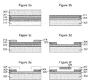
- Figures 3a-e show another method of forming a field-effect apparatus (cross-section), this time comprising a top gate electrode 306.
- the layer of polymeric material 302 is deposited without the prior deposition of the dielectric and conductive layers ( Figure 3a ).
- the release material 313 and carrier wafer 312 are then removed as before and the stack is turned upside down ( Figure 3b ).
- a layer of dielectric material 307 can be deposited onto the channel 301 and source 303 and drain 304 electrodes to form a gate insulator ( Figure 3e ).
- a layer of conductive material 306 can then be deposited on top of the dielectric layer 307 to form a gate electrode ( Figure 3f ).
- the gate electrode 306 is localised to the channel region between the source 303 and drain 304 electrodes (e.g.
- the layers of dielectric 307 and conductive 306 material are deposited such that the supporting substrate 302 is separated from the layers of dielectric 307 and conductive 306 material by the channel member 301 to form a top gate electrode 306.
- Figures 4a-c show various embodiments of a field-effect apparatus (in plan-view) comprising a plurality of channel members 401a-c rather than a single channel member 401.
- This may form the basis of an electronic device which requires a high density of transistors or a sensor which is capable of detecting multiple stimuli, and can be fabricated by suitable patterning of the layer of channel material.
- the layer of catalyst material may be pre-patterned before growing the layer of channel material to form the plurality of channel members 401a-c by selective growth.
- a continuous layer of channel material may be patterned after growth.
- the latter may be performed by depositing respective layers of dielectric material and photoresist on the layer of channel material such that the photoresist is separated from the layer of channel material by the layer of dielectric material, patterning the layer of photoresist, and etching the layers of channel and dielectric material through the patterned layer of photoresist.
- the layer of dielectric material is used to prevent contact between the photoresist and the channel member 401 in order to reduce contamination at the surface of the channel member 401.
- the layers of catalyst and conductive material have been patterned to form a respective source electrode 403a-c, a respective drain electrode 404a-c and a respective gate electrode 406a-c for each channel member 401 a-c. In some scenarios, however, it may be acceptable to use the same source 403, drain 404 or gate 406 electrode for multiple channel members 401a-c. Using the same electrode for multiple channel members 401a-c can simplify the fabrication process and device complexity and can also reduce material costs.
- the layers of catalyst and conductive material have been patterned to form a common source electrode 403, a common drain electrode 404 and a common gate electrode 406 for the plurality of channel members 401a-c.
- some of the source 403a-c, drain 404a-c and/or gate 406a-c electrodes may be associated with respective channel members and some may be associated with multiple channel members.
- Figure 4c is one such example, which comprises two channel members 401 a,b formed from a single strip of channel material (in contrast to the examples of Figures 4a and 4b which comprise separate strips of channel material).
- the channel members 401 a,b have their own source 403a,b and gate 406a,b electrodes but share a common drain electrode 404.
- the electrical currents flowing through each channel member 401a,b are in opposite directions (as indicated by the arrows).
- the current flow is in the same direction for each channel member 401a-c.
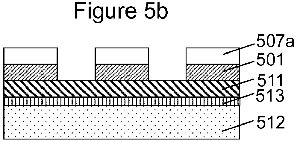
- Figures 5a-f illustrate another method of forming a field-effect apparatus (in cross-section).
- a layer of channel material 501 is grown on a growth wafer 510 followed by the deposition of a layer of dielectric material 507a ( Figure 5a ).
- the layers of channel 501 and dielectric 507a material are then patterned (e.g. by selectively etching the channel 501 and dielectric 507a materials through a photoresist mask) to define the channel member ( Figure 5b ).
- a layer of conductive material is then deposited onto the layer of catalyst material 511 through the patterned layers of channel 501 and dielectric 507a material to form discrete regions of conductive material 515.
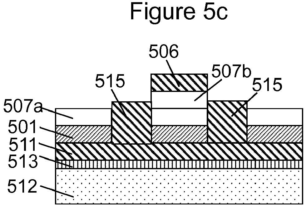
- a further layer of dielectric material 507b is selectively deposited over the channel member 501 followed by a layer of conductive material to form a gate electrode 506 ( Figure 5c ).
- the further layer of dielectric material 507b helps to prevent contact between the gate electrode 506 and the underlying channel member 501 (described in more detail with reference to Figures 6a-c ), as well as between the gate electrode 506 and the discrete regions of conductive material 515. It also allows the thickness of the dielectric material 507b forming the gate insulator to be independent of the thickness of the dielectric material 507a elsewhere.
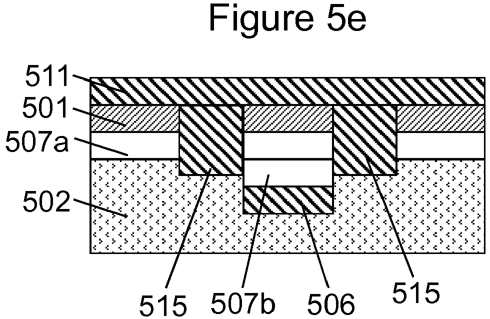
- a layer of polymeric material 502 is then deposited on top of the stack ( Figure 5d ), the release material 513 and carrier wafer 512 are removed as before and the stack is turned upside down ( Figure 5e ).
- the polymeric material 502 may be deposited as a liquid polymer and cured, or as a polymer foil and embossed. Either way, the layer of polymeric material 502 encapsulates the gate electrode 506 and exposed regions of conductive material 515.
- the layer of catalyst material 511 is patterned to form electrical contacts 516 overlying the channel member 501 and respective discrete regions of conductive material 515 ( Figure 5f ). In this way, the electrical contacts 516 and respective discrete regions of conductive material 515 together form source 503 and drain 504 electrodes.
- any channel material 501 which is not used to form the channel members may be removed to help prevent short circuits between adjacent channel members or their respective electrodes 503, 504.
- Figures 11a-f show a modified version of the process of Figures 5a-f in which the excess channel material 1101 is etched away before formation of the source 1103, drain 1104 and gate 1106 electrodes.
- the layers of channel 1101 and dielectric 1107a material are patterned to define the channel member (e.g. by etching through a photoresist mask). This time, however, the layers of channel 1101 and dielectric 1107a material are patterned such that all material outside the channel region is removed by the etching step ( Figure 11 b) .
- the further layer of dielectric material 1107b is then selectively deposited over the channel member (e.g.
- a further mask e.g. photoresist
- a further mask can then be used to selectively deposit discrete regions of conductive material 1115 for the source 1103 and drain 1104 electrodes ( Figure 11c ).
- the same layer of conductive material may be used for the source 1103, drain 1104 and gate 1106 electrodes.
- the mask used during deposition of the further layer of dielectric material 1107b is removed before selective deposition of the conductive material.
- the remaining steps of the process e.g. Figures 11d-f ) are the same as those described with reference to Figures 5d-f .
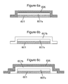
- Figures 6a-c show how the further layer of dielectric material 507b is Figure 5c can help to prevent contact between the gate electrode 506 and the underlying channel member 501.
- These figures are cross-sectional views of the corresponding layers of Figure 5c perpendicular to the cross-section of Figure 5c (i.e. into the page).
- deposition of the layer of conductive material 606 on top of the channel member 601 and layer of dielectric material 607a can result in contact between the conductive material 606 and the channel material 601 at the edges of the channel member which may create a short circuit.
- the reason for extending the layer of conductive material 606 down the edges of the channel member 601 is to enable connection of the gate electrode 606 to a power supply for provision of a gate voltage.
- a further layer of dielectric material 607b on top of the first layer of dielectric material 607a ( Figure 6b )
- the edges of the channel member 601 can be insulated from the layer of subsequently deposited conductive material 606 ( Figure 6c ).
- the further layer of dielectric material 607b may be deposited at the edges of the channel member 601 only so as not to increase the distance between the gate electrode 606 and the channel member 601.
- Figures 7a-e show a further method of forming a field-effect apparatus.
- steps 7a-d are identical to steps 3a-d of the method described with reference to Figure 3 .
- the method instead of depositing respective layers of dielectric and conductive material onto the channel member 701, the method comprises depositing a layer of sensor material 717 (e.g. by spin casting, inkjet printing or stamping) configured to vary the flow of electrical current through the channel member 701 in response to an applied stimulus.
- the layer of sensor material 717 functionalises or activates the channel member 701 such that the applied stimulus is able to gate the channel member 701 instead of a gate electrode, thus enabling detection of the stimulus based on the variation in electrical current.
- the sensor material 717 may be configured to enable detection of any stimulus provided that the interaction of that stimulus with the sensor material 717 results in a change in electrical current through the channel member.
- the sensor material 717 may comprise one or more of a quantum dot material for sensing electromagnetic radiation, a pyroelectric material for sensing temperature, a piezoelectric material for sensing mechanical stress, a chemical binding agent for sensing a chemical species, and a biological receptor for sensing a biological species.
- the layer of sensor material 717 comprises an antibody configured to bind to a charged species 718 in the surrounding environment such that the charged species 718 is in sufficient proximity to the channel member 701 to cause a variation in electrical current.
- a bottom gate electrode could be used to tune the conductance/conductivity of the channel member 701.
- a number of different materials may be used in the above-mentioned processes.
- One particular example involves the use of a graphene channel member grown on a silicon carrier wafer using copper as the catalyst material and silicon oxide as the release material.
- the dielectric material may comprise aluminium oxide
- the conductive material may comprise copper
- the polymeric material may comprise polyimide
- the sensor material may comprise PbS quantum dots.
- This example benefits from the high mobility of graphene, the quantum efficiency of PbS quantum dots and the mechanical resilience of polyimide, thus rendering it suitable for use as a reversibly deformable (e.g. flexible, stretchable and/or compressible) graphene field-effect transistor (GFET) photodetector.
- GFET graphene field-effect transistor
- the channel material may comprise one or more of graphene, a two-dimensional chalcogenide, MoS 2 , WS 2 , MoSe 2 , WSe 2 and WTe 2 ;
- the catalyst and conductive materials may comprise one or more of a metal, an alloy, gold, silver, aluminium, copper, nickel, platinum, germanium and indium tin oxide (the catalyst material should be electrically conductive to enable its use as source and drain electrodes);
- the polymeric material may comprise one or more of HD MicrosystemsTM PI-2545, PI-2610 or PI-2525, polyimide, polyethylene naphthalate and polyethylene terephthalate;
- the dielectric material may comprise one or more of Si 3 N 4 , Al 2 O 3 , hBN, SiO 2 and HfO 2 ;
- the release material may comprise one or more of a refractory metal, a ceramic, SiO, SiO 2 , Mo, W, Al 2
- a number of different types of sensor material may be used depending on the specific stimuli being detected. These include, but are not limited to, one or more of: a quantum dot material (e.g. CdSe, CdS, PbSe, PbS, ZnO, ZnS, CZTS, Cu 2 S, Bi 2 S 3 , Ag 2 S, HgTe, CdSe, CdHgTe, InAs, InSb, Ge or CIS); a pyroelectric material (e.g. polyvinylidine fluoride, P(VDF-trifluoroethylene), lithium tantalate and gallium nitride); a piezoelectric material (e.g.
- a quantum dot material e.g. CdSe, CdS, PbSe, PbS, ZnO, ZnS, CZTS, Cu 2 S, Bi 2 S 3 , Ag 2 S, HgTe, CdSe, CdHgTe, InAs
- polyvinylidene fluoride lead zirconium titanate, barium titanate and zinc oxide
- a chemical binding agent e.g. an alkanethiol and an alkoxysilane
- a biological receptor e.g. an antibody
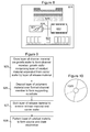
- Figure 8 shows one example of an apparatus 819 at least partly formed using a method described herein.
- the apparatus 819 may be one or more of an electronic device, a portable electronic device, a portable telecommunications device, a mobile phone, a personal digital assistant, a tablet, a phablet, a desktop computer, a laptop computer, a server, a smartphone, a smartwatch, smart eyewear, a sensor, a photodetector, a field-effect transistor, and a module for one or more of the same.
- the apparatus 819 comprises the various components described previously (denoted collectively by reference numeral 820), a power source 821, a processor 822 and a storage medium 823, which are electrically connected to one another by a data bus 824.
- the processor 822 is configured for general operation of the apparatus 819 by providing signalling to, and receiving signalling from, the other components to manage their operation.
- the storage medium 823 is configured to store computer code configured to perform, control or enable operation of the apparatus 819.
- the storage medium 823 may also be configured to store settings for the other components.
- the processor 822 may access the storage medium 823 to retrieve the component settings in order to manage the operation of the other components.
- the power source 821 is configured to apply a voltage between the source and drain electrodes to enable a flow of electrical current through the channel member, and apply a gate voltage to the gate electrode to cause a detectable change in the flow of electrical current.
- the components 820 may act as an electronic switch within the circuitry of the apparatus 819.
- the processor 822 may be a microprocessor, including an Application Specific Integrated Circuit (ASIC).
- the storage medium 823 may be a temporary storage medium such as a volatile random access memory.
- the storage medium 823 may be a permanent storage medium 823 such as a hard disk drive, a flash memory, or a non-volatile random access memory.
- the power source 821 may comprise one or more of a primary battery, a secondary battery, a capacitor, a supercapacitor and a battery-capacitor hybrid.
- Figure 9 shows schematically the main steps 925-928 of a method of making a field-effect apparatus.
- the method generally comprises: growing a layer of channel material on a growth wafer to form a channel member, the growth wafer comprising a layer of catalyst material separated from a carrier wafer by a layer of release material 925; depositing a layer of polymeric material over the formed channel member to form a supporting substrate 926; etching the layer of release material to remove the release material and carrier wafer 927; and patterning the layer of catalyst material to form source and drain electrodes 928.
- Figure 10 illustrates schematically a computer/processor readable medium 1029 providing a computer program according to one embodiment.
- the computer program may comprise computer code configured to perform, control or enable one or more of the method steps 925-928 of Figure 9 . Additionally or alternatively, the computer program may comprise computer code configured to apply a voltage between the source and drain electrodes to enable a flow of electrical current through the channel member; and apply a gate voltage to the gate electrode to cause a detectable change in the flow of electrical current.
- the computer/processor readable medium 1029 is a disc such as a digital versatile disc (DVD) or a compact disc (CD).
- DVD digital versatile disc
- CD compact disc
- the computer/processor readable medium 1029 may be any medium that has been programmed in such a way as to carry out an inventive function.
- the computer/processor readable medium 1029 may be a removable memory device such as a memory stick or memory card (SD, mini SD, micro SD or nano SD).
- feature number 1 can also correspond to numbers 101, 201, 301 etc. These numbered features may appear in the figures but may not have been directly referred to within the description of these particular embodiments. These have still been provided in the figures to aid understanding of the further embodiments, particularly in relation to the features of similar earlier described embodiments.
- any mentioned apparatus/device and/or other features of particular mentioned apparatus/device may be provided by apparatus arranged such that they become configured to carry out the desired operations only when enabled, e.g. switched on, or the like. In such cases, they may not necessarily have the appropriate software loaded into the active memory in the non-enabled (e.g. switched off state) and only load the appropriate software in the enabled (e.g. on state).
- the apparatus may comprise hardware circuitry and/or firmware.
- the apparatus may comprise software loaded onto memory.
- Such software/computer programs may be recorded on the same memory/processor/functional units and/or on one or more memories/processors/functional units.
- a particular mentioned apparatus/device may be pre-programmed with the appropriate software to carry out desired operations, and wherein the appropriate software can be enabled for use by a user downloading a "key", for example, to unlock/enable the software and its associated functionality.
- Advantages associated with such embodiments can include a reduced requirement to download data when further functionality is required for a device, and this can be useful in examples where a device is perceived to have sufficient capacity to store such pre-programmed software for functionality that may not be enabled by a user.
- any mentioned apparatus/circuitry/elements/processor may have other functions in addition to the mentioned functions, and that these functions may be performed by the same apparatus/circuitry/elements/processor.
- One or more disclosed aspects may encompass the electronic distribution of associated computer programs and computer programs (which may be source/transport encoded) recorded on an appropriate carrier (e.g. memory, signal).
- any "computer” described herein can comprise a collection of one or more individual processors/processing elements that may or may not be located on the same circuit board, or the same region/position of a circuit board or even the same device. In some embodiments one or more of any mentioned processors may be distributed over a plurality of devices. The same or different processor/processing elements may perform one or more functions described herein.
- signal may refer to one or more signals transmitted as a series of transmitted and/or received signals.
- the series of signals may comprise one, two, three, four or even more individual signal components or distinct signals to make up said signalling. Some or all of these individual signals may be transmitted/received simultaneously, in sequence, and/or such that they temporally overlap one another.
- processors and memory may comprise a computer processor, Application Specific Integrated Circuit (ASIC), field-programmable gate array (FPGA), and/or other hardware components that have been programmed in such a way to carry out the inventive function.
- ASIC Application Specific Integrated Circuit
- FPGA field-programmable gate array
Landscapes
- Thin Film Transistor (AREA)
Abstract
growing a layer of channel material (501), preferably graphene, on a growth wafer (512) to form a channel member, the growth wafer comprising a layer of catalyst material (511) separated from a carrier wafer (512) by a layer of release material (513), the catalyst material serving as a seed layer for growing the layer of channel material;
depositing a layer of polymeric material (502) over the formed channel member to form a supporting substrate for the layers of catalyst and channel material;
etching the layer of release material (513) to remove the release material and carrier wafer; and
patterning the layer of catalyst material (511) to form source and drain electrodes (516) configured to enable a flow of electrical current through the channel member.


Description
- The present disclosure relates particularly to field-effect devices, associated methods and apparatus. Certain embodiments specifically concern a method of making a field-effect apparatus which results in less contamination in the end product than prior art methods. This reduction in contamination can provide an increase in charge carrier mobility and a reduction in contact resistance. Certain aspects/embodiments may relate to sensing (e.g. biosensing, optical sensing, deformation sensing, etc) for healthcare, automotive or wearable applications. Other aspects/embodiments may relate to field-effect transistors suitable for portable electronic devices, in particular, so-called hand-portable electronic devices which may be hand-held in use (although they may be placed in a cradle in use). Such hand-portable electronic devices include so-called Personal Digital Assistants (PDAs) and tablet PCs.
- The portable electronic devices/apparatus according to one or more disclosed example aspects/embodiments may provide one or more audio/text/video communication functions (e.g. tele-communication, video-communication, and/or text transmission, Short Message Service (SMS)/ Multimedia Message Service (MMS)/emailing functions, interactive/non-interactive viewing functions (e.g. web-browsing, navigation, TV/program viewing functions), music recording/playing functions (e.g. MP3 or other format and/or (FM/AM) radio broadcast recording/playing), downloading/sending of data functions, image capture function (e.g. using a (e.g. in-built) digital camera), and gaming functions.
- Research is currently being done to develop new field-effect devices with improved physical and electrical properties for use in a variety of applications.
- The listing or discussion of a prior-published document or any background in this specification should not necessarily be taken as an acknowledgement that the document or background is part of the state of the art or is common general knowledge.
- According to a first aspect, there is provided a method comprising:
- growing a layer of channel material on a growth wafer to form a channel member, the growth wafer comprising a layer of catalyst material separated from a carrier wafer by a layer of release material, the catalyst material serving as a seed layer for growing the layer of channel material;
- depositing a layer of polymeric material over the formed channel member to form a supporting substrate for the layers of catalyst and channel material;
- etching the layer of release material to remove the release material and carrier wafer; and
- patterning the layer of catalyst material to form source and drain electrodes configured to enable a flow of electrical current through the channel member.
- The method may comprise depositing respective layers of dielectric and conductive material on the channel member such that the layer of conductive material is separated from channel member by the layer of dielectric material, the layer of conductive material forming a gate electrode configured to enable the flow of electrical current through the channel member to be varied by a voltage applied to the gate electrode.
- The method may comprise depositing the layers of dielectric and conductive material between the channel member and supporting substrate to form a back gate electrode.
- The method may comprise depositing the layers of dielectric and conductive material such that the supporting substrate is separated from the layers of dielectric and conductive material by the channel member to form a top gate electrode.
- The method may comprise patterning the layers of channel and conductive material to form a plurality of gated channel members.
- The method may comprise patterning one or more of the layers of catalyst and conductive material to form at least one of a common source, common drain and common gate electrode for the plurality of gated channel members and/or at least one of a respective source, respective drain and respective gate electrode for each gated channel member.
- Patterning the layer of channel material may comprise pre-patterning the layer of catalyst material before growing the layer of channel material to form the plurality of channel members by selective growth.
- Patterning the layer of channel material may comprise:
- depositing respective layers of dielectric material and photoresist on the layer of channel material such that the photoresist is separated from the layer of channel material by the layer of dielectric material;
- patterning the layer of photoresist; and
- etching the layers of channel and dielectric material through the patterned layer of photoresist.
- Forming the source and drain electrodes may further comprise:
- depositing respective layers of dielectric material and photoresist on the channel member such that the photoresist is separated from the channel member by the layer of dielectric material;
- patterning the layer of photoresist;
- etching the channel member and layer of dielectric material through the patterned layer of photoresist;
- depositing a layer of conductive material onto the layer of catalyst material through the etched channel member and layer of dielectric material to form discrete regions of conductive material; and
- patterning the layer of catalyst material to form electrical contacts overlying the channel member and respective discrete regions of conductive material, the electrical contacts and respective discrete regions of conductive material together forming the source and drain electrodes.
- The method may comprise:
- selectively depositing a further layer of dielectric material over the etched channel member; and
- depositing the layer of conductive material onto the further layer of dielectric material such that the layer of conductive material is separated from the channel member by the further layer of dielectric material, the layer of conductive material forming a gate electrode configured to enable the flow of electrical current through the channel member to be varied by a voltage applied to the gate electrode.
- The method may comprise depositing a layer of sensor material onto the channel member, the sensor material configured to vary the flow of electrical current through the channel member in response to an applied stimulus.
- The layer of sensor material may be configured to vary the flow of electrical current in response to one or more of the following stimuli: electromagnetic radiation, temperature, mechanical stress, a chemical species and a biological species.
- The polymeric material may be configured to form a supporting substrate that is one or more of substantially reversibly deformable, substantially reversibly stretchable, substantially reversibly flexible and substantially reversibly compressible.
- The layer of channel material may be grown using chemical vapour deposition.
- The layer of channel material may comprise one or more of graphene, a two-dimensional chalcogenide, MoS2, WS2, MoSe2, WSe2 and WTe2.
- One or more of the layers of catalyst and conductive material may comprise at least one of a metal, an alloy, gold, silver, aluminium, copper, nickel, platinum, germanium and indium tin oxide.
- The layer of polymeric material may comprise one or more of PI-2545, PI-2610, PI-2525, polyimide, polyethylene naphthalate and polyethylene terephthalate.
- The layer(s) of dielectric material may comprise one or more of Si3N4, Al2O3, hBN, SiO2 and HfO2.
- The layer of release material may comprise one or more of a refractory metal, a ceramic, SiO, SiO2, Mo, W, Al2O3 and Si3N4.
- The carrier wafer may comprise one or more of silicon, quartz and sapphire.
- The sensor material may comprise one or more of a quantum dot material, a pyroelectric material, a piezoelectric material, a chemical binding agent and a biological receptor.
- The quantum dot material may comprise one or more of CdSe, CdS, PbSe, PbS, ZnO, ZnS, CZTS, Cu2S, Bi2S3, Ag2S, HgTe, CdSe, CdHgTe, InAs, InSb, Ge and CIS.
- The pyroelectric material may comprise one or more of polyvinylidine fluoride, P(VDF-trifluoroethylene), lithium tantalate and gallium nitride.
- The piezoelectric material may comprise one or more of polyvinylidene fluoride, lead zirconium titanate, barium titanate and zinc oxide.
- The chemical binding agent may comprise one or more of an alkanethiol and an alkoxysilane.
- The biological receptor may comprise an antibody.
- According to a further aspect, there is provided an apparatus formed by any method described herein.
- One or more of the source, drain and gate electrodes of the apparatus may be at least partially embedded within the polymeric material.
- The apparatus may be one or more of an electronic device, a portable electronic device, a portable telecommunications device, a mobile phone, a personal digital assistant, a tablet, a phablet, a desktop computer, a laptop computer, a server, a smartphone, a smartwatch, smart eyewear, a sensor, a photodetector, a field-effect transistor, and a module for one or more of the same.
- The steps of any method disclosed herein do not have to be performed in the exact order disclosed, unless explicitly stated or understood by the skilled person.
- Throughout the present specification, descriptors relating to relative orientation and position, such as "top", "bottom", "upper", "lower", "above" and "below", as well as any adjective and adverb derivatives thereof, are used in the sense of the orientation of the apparatus as presented in the drawings. However, such descriptors are not intended to be in any way limiting to an intended use of the described or claimed invention.
- Corresponding computer programs for implementing one or more steps of the methods disclosed herein are also within the present disclosure and are encompassed by one or more of the described example embodiments.
- One or more of the computer programs may, when run on a computer, cause the computer to configure any apparatus, including a circuit, controller, or device disclosed herein or perform any method disclosed herein. One or more of the computer programs may be software implementations, and the computer may be considered as any appropriate hardware, including a digital signal processor, a microcontroller, and an implementation in read only memory (ROM), erasable programmable read only memory (EPROM) or electronically erasable programmable read only memory (EEPROM), as non-limiting examples. The software may be an assembly program.
- One or more of the computer programs may be provided on a computer readable medium, which may be a physical computer readable medium such as a disc or a memory device, or may be embodied as a transient signal. Such a transient signal may be a network download, including an internet download.
- The present disclosure includes one or more corresponding aspects, example embodiments or features in isolation or in various combinations whether or not specifically stated (including claimed) in that combination or in isolation. Corresponding means for performing one or more of the discussed functions are also within the present disclosure.
- The above summary is intended to be merely exemplary and non-limiting.
- A description is now given, by way of example only, with reference to the accompanying drawings, in which:-
-
Figure 1 shows a conventional field-effect transistor (cross-section); -
Figures 2a-d show one method of forming a field-effect apparatus (cross-section); -
Figures 3a-f show another method of forming a field-effect apparatus (cross-section); -
Figures 4a-c show various embodiments of a field-effect apparatus comprising a plurality of gated graphene channels (plan view); -
Figures 5a-f show another method of forming a field-effect apparatus (cross-section); -
Figures 6a-c show a method of preventing contact between the gate electrode and channel member (cross-section); -
Figures 7a-e show another method of forming a field-effect apparatus (cross-section); -
Figure 8 shows one example of an apparatus described herein (schematic); -
Figure 9 shows the main steps of a method described herein (flow chart); -
Figure 10 shows a computer-readable medium comprising a computer program configured to perform, control or enable a method described herein (schematic); andFigures 11a-f show another method of forming a field-effect apparatus (cross-section). - One or more disclosed embodiments of the present apparatus relate to field-effect transistors (FETs). An FET is a type of transistor in which an electrical current is passed through a channel, the conductance (or conductivity) of which can be controlled by a transverse electric field.
-
Figure 1 shows a conventional FET in cross-section. As shown in this figure, a semiconductor channel 101 (such as p-type silicon) is supported on asubstrate 102 and connected tometal source 103 and drain 104 electrodes. A current enters and exits the channel via thesource 103 and drain 104 electrodes, respectively, by applying a potential difference (V) 105 across thechannel 101. The conductance of thechannel 101 between thesource 103 and drain 104 electrodes is switched on and off by a third electrode (the gate electrode 106) capacitively coupled through athin dielectric layer 107. The conductance may be determined by measuring the current through the channel 101 (using anammeter 108, for example) and dividing by the potential difference (V) 105. With p-type silicon (or another p-type semiconductor), application of a positive gate voltage (VG) depletes the charge carriers (creating adepletion region 109 in the channel 101) and reduces the conductance, whilst applying a negative gate voltage (VG) leads to an accumulation of charge carriers (creating a conductive region) and an increase in conductance. - Two factors which are important in defining the performance of FETs are the mobility of the charge carriers through the channel, and the contact resistance of the source and drain electrodes with the channel. It has been found, however, that the mobility and contact resistance are adversely affected by contamination at the surface of the channel where it can produce charge concentrations, scattering, locations for trapped water, and can inhibit physical and electrical contact. Contamination of the channel surface tends to increase with the number of processing steps performed on top of the channel (especially photolithography) and the transfer of the channel material from one substrate to another.
- There will now be described a number of methods of forming a field-effect apparatus that may help to reduce the amount of contamination at the channel surface.
-
Figures 2a-d illustrate one method of forming a field-effect apparatus, shown as a series of cross-sectional process steps. First, a layer ofchannel material 201 is grown (e.g. via chemical vapour deposition) on agrowth wafer 210 to form a channel member. Thegrowth wafer 210 comprises a layer ofcatalyst material 211 separated from a carrier wafer 212 by a layer of release material 213, thecatalyst material 211 serving as a seed layer for growing the layer ofchannel material 201. Respective layers ofdielectric 207 and conductive 206 material are then deposited on thechannel member 201 such that the layer ofconductive material 206 is separated from thechannel member 201 by the layer ofdielectric material 207 to form a gate electrode. The layer ofdielectric material 207 also acts as a barrier layer to protect thechannel member 201 from water in humid environments or solvents (which can result in p-type channel FETs requiring large gate voltage biases to reach their Dirac points). The layer ofdielectric material 207 may be deposited using atomic layer deposition, and the layer ofconductive material 206 may be deposited by evaporation or sputtering. After deposition of the layers ofdielectric 207 and conductive 206 material, a layer ofpolymeric material 202 is deposited over thechannel member 201 to form a supporting substrate for the layers ofcatalyst 211 and channel material 201 (Figure 2a ). This may be performed via spin coating, bar coating or spray coating a liquid polymer and curing to cross-link, or by hot embossing a polymer foil (i.e. heating above the glass transition temperature and imprinting). - The layer of release material 213 is then etched (e.g. wet chemical etching using hydrofluoric acid if etching silicon oxide) to remove the release material 213 and carrier wafer 212, and the stack is turned upside down (e.g. using the
polymeric supporting substrate 202 for handling) so that the layer ofpolymeric material 202 is at the bottom of the stack (Figure 2b ). Aphotoresist mask 214 is then formed on top of the layer ofcatalyst material 211 to allow corresponding patterning of the catalyst material 211 (Figure 2c ). Themask 214 may be formed by selectively exposing the photoresist to incident electromagnetic radiation and developing the exposed regions to remove the unwanted photoresist. The layer ofcatalyst material 211 is then etched through thephotoresist mask 214 to formsource 203 and drain 204 electrodes (Figure 2d ). - This method addresses the above-mentioned contamination issue in a number of different ways. Firstly, by depositing the layer of
polymeric material 202 on top of the stack and then removing the carrier wafer 212, there is no need to transfer thechannel member 201 from thegrowth substrate 210 to thepolymeric support substrate 202. Secondly, at no point in the process does the layer ofchannel material 201 come into contact with thephotoresist 214. This is because thesource 203 and drain 204 electrodes are formed by selectively etching the layer ofcatalyst material 211 through a resistmask 214 rather than by selectively depositing a layer of conductive material through the resistmask 214. Thirdly, since thesource 203 and drain 204 electrodes are formed from the layer ofcatalyst material 211 on which thechannel member 201 is grown, thesource 203 and drain 204 electrodes are adhered more strongly to thechannel member 201 than they would be if theelectrodes - As mentioned with reference to
Figure 1 , thesource 203 and drain 204 electrodes are configured to enable a flow of electrical current through thechannel member 201, and thegate electrode 206 is configured to enable the flow of electrical current through thechannel member 201 to be varied by a voltage applied to thegate electrode 206. In this example, the layers ofdielectric 207 and conductive 206 material are deposited between thechannel member 201 and supportingsubstrate 202 to form aback gate electrode 206. Theback gate electrode 206 is formed as a continuous layer of conductive material which may facilitate control of the electrical current by generating electric fields which are able to interact with the full length of thechannel member 201. It is, however, also possible to form a discrete back gate electrode by patterning the layer ofconductive material 206 before deposition of the layer of polymeric material 202 (not shown). -
Figures 3a-e show another method of forming a field-effect apparatus (cross-section), this time comprising atop gate electrode 306. To achieve this, the layer ofpolymeric material 302 is deposited without the prior deposition of the dielectric and conductive layers (Figure 3a ). The release material 313 and carrier wafer 312 are then removed as before and the stack is turned upside down (Figure 3b ). Once thephotoresist mask 314 has been formed on top of the layer of catalyst material 311 (Figure 3c ), and thecatalyst material 311 etched through thephotoresist mask 314 to formsource 303 and drain 304 electrodes (Figure 3d ), a layer ofdielectric material 307 can be deposited onto thechannel 301 andsource 303 and drain 304 electrodes to form a gate insulator (Figure 3e ). A layer ofconductive material 306 can then be deposited on top of thedielectric layer 307 to form a gate electrode (Figure 3f ). In this example, thegate electrode 306 is localised to the channel region between thesource 303 and drain 304 electrodes (e.g. by deposition through a mask), but a continuous layer covering thecomplete dielectric layer 307 could also be used for ease of fabrication without adversely affecting operation of the apparatus. With this method, therefore, the layers ofdielectric 307 and conductive 306 material are deposited such that the supportingsubstrate 302 is separated from the layers ofdielectric 307 and conductive 306 material by thechannel member 301 to form atop gate electrode 306. -
Figures 4a-c show various embodiments of a field-effect apparatus (in plan-view) comprising a plurality ofchannel members 401a-c rather than a single channel member 401. This may form the basis of an electronic device which requires a high density of transistors or a sensor which is capable of detecting multiple stimuli, and can be fabricated by suitable patterning of the layer of channel material. For example, the layer of catalyst material may be pre-patterned before growing the layer of channel material to form the plurality ofchannel members 401a-c by selective growth. Alternatively, a continuous layer of channel material may be patterned after growth. The latter may be performed by depositing respective layers of dielectric material and photoresist on the layer of channel material such that the photoresist is separated from the layer of channel material by the layer of dielectric material, patterning the layer of photoresist, and etching the layers of channel and dielectric material through the patterned layer of photoresist. Here, the layer of dielectric material is used to prevent contact between the photoresist and the channel member 401 in order to reduce contamination at the surface of the channel member 401. - In the example shown in
Figure 4a , the layers of catalyst and conductive material have been patterned to form arespective source electrode 403a-c, arespective drain electrode 404a-c and arespective gate electrode 406a-c for each channel member 401 a-c. In some scenarios, however, it may be acceptable to use thesame source 403, drain 404 orgate 406 electrode formultiple channel members 401a-c. Using the same electrode formultiple channel members 401a-c can simplify the fabrication process and device complexity and can also reduce material costs. In the example shown inFigure 4b , the layers of catalyst and conductive material have been patterned to form acommon source electrode 403, acommon drain electrode 404 and acommon gate electrode 406 for the plurality ofchannel members 401a-c. In other examples, some of thesource 403a-c, drain 404a-c and/orgate 406a-c electrodes may be associated with respective channel members and some may be associated with multiple channel members.Figure 4c is one such example, which comprises twochannel members 401 a,b formed from a single strip of channel material (in contrast to the examples ofFigures 4a and 4b which comprise separate strips of channel material). In this example, thechannel members 401 a,b have theirown source 403a,b andgate 406a,b electrodes but share acommon drain electrode 404. As a result, the electrical currents flowing through eachchannel member 401a,b are in opposite directions (as indicated by the arrows). In the examples ofFigures 4a and 4b , on the other hand, the current flow is in the same direction for eachchannel member 401a-c. -
Figures 5a-f illustrate another method of forming a field-effect apparatus (in cross-section). First, a layer ofchannel material 501 is grown on agrowth wafer 510 followed by the deposition of a layer ofdielectric material 507a (Figure 5a ). The layers ofchannel 501 and dielectric 507a material are then patterned (e.g. by selectively etching thechannel 501 and dielectric 507a materials through a photoresist mask) to define the channel member (Figure 5b ). A layer of conductive material is then deposited onto the layer ofcatalyst material 511 through the patterned layers ofchannel 501 and dielectric 507a material to form discrete regions ofconductive material 515. After this, a further layer ofdielectric material 507b is selectively deposited over thechannel member 501 followed by a layer of conductive material to form a gate electrode 506 (Figure 5c ). The further layer ofdielectric material 507b helps to prevent contact between thegate electrode 506 and the underlying channel member 501 (described in more detail with reference toFigures 6a-c ), as well as between thegate electrode 506 and the discrete regions ofconductive material 515. It also allows the thickness of thedielectric material 507b forming the gate insulator to be independent of the thickness of thedielectric material 507a elsewhere. - A layer of
polymeric material 502 is then deposited on top of the stack (Figure 5d ), therelease material 513 andcarrier wafer 512 are removed as before and the stack is turned upside down (Figure 5e ). As mentioned previously, thepolymeric material 502 may be deposited as a liquid polymer and cured, or as a polymer foil and embossed. Either way, the layer ofpolymeric material 502 encapsulates thegate electrode 506 and exposed regions ofconductive material 515. Finally, the layer ofcatalyst material 511 is patterned to formelectrical contacts 516 overlying thechannel member 501 and respective discrete regions of conductive material 515 (Figure 5f ). In this way, theelectrical contacts 516 and respective discrete regions ofconductive material 515 together formsource 503 and drain 504 electrodes. - If the process illustrated in
Figures 5a-f is to be used to form a plurality of gated channel members, anychannel material 501 which is not used to form the channel members may be removed to help prevent short circuits between adjacent channel members or theirrespective electrodes -
Figures 11a-f show a modified version of the process ofFigures 5a-f in which theexcess channel material 1101 is etched away before formation of thesource 1103,drain 1104 andgate 1106 electrodes. As with the previous process, the layers ofchannel 1101 and dielectric 1107a material are patterned to define the channel member (e.g. by etching through a photoresist mask). This time, however, the layers ofchannel 1101 and dielectric 1107a material are patterned such that all material outside the channel region is removed by the etching step (Figure 11 b) . The further layer ofdielectric material 1107b is then selectively deposited over the channel member (e.g. using a photoresist mask on top of the layer of catalyst material 1111) followed by the deposition of a layer of conductive material to form thegate electrode 1106. Once the mask is removed, a further mask (e.g. photoresist) can then be used to selectively deposit discrete regions ofconductive material 1115 for thesource 1103 and drain 1104 electrodes (Figure 11c ). In some cases, the same layer of conductive material may be used for thesource 1103,drain 1104 andgate 1106 electrodes. To achieve this, the mask used during deposition of the further layer ofdielectric material 1107b is removed before selective deposition of the conductive material. The remaining steps of the process (e.g.Figures 11d-f ) are the same as those described with reference toFigures 5d-f . -
Figures 6a-c show how the further layer ofdielectric material 507b isFigure 5c can help to prevent contact between thegate electrode 506 and theunderlying channel member 501. These figures are cross-sectional views of the corresponding layers ofFigure 5c perpendicular to the cross-section ofFigure 5c (i.e. into the page). As illustrated inFigure 6a , deposition of the layer ofconductive material 606 on top of thechannel member 601 and layer ofdielectric material 607a can result in contact between theconductive material 606 and thechannel material 601 at the edges of the channel member which may create a short circuit. The reason for extending the layer ofconductive material 606 down the edges of thechannel member 601 is to enable connection of thegate electrode 606 to a power supply for provision of a gate voltage. By depositing a further layer ofdielectric material 607b on top of the first layer ofdielectric material 607a (Figure 6b ), however, the edges of thechannel member 601 can be insulated from the layer of subsequently deposited conductive material 606 (Figure 6c ). In some cases, the further layer ofdielectric material 607b may be deposited at the edges of thechannel member 601 only so as not to increase the distance between thegate electrode 606 and thechannel member 601. -
Figures 7a-e show a further method of forming a field-effect apparatus. As can be seen from these figures, steps 7a-d are identical to steps 3a-d of the method described with reference toFigure 3 . This time, however, instead of depositing respective layers of dielectric and conductive material onto thechannel member 701, the method comprises depositing a layer of sensor material 717 (e.g. by spin casting, inkjet printing or stamping) configured to vary the flow of electrical current through thechannel member 701 in response to an applied stimulus. The layer ofsensor material 717 functionalises or activates thechannel member 701 such that the applied stimulus is able to gate thechannel member 701 instead of a gate electrode, thus enabling detection of the stimulus based on the variation in electrical current. In practice, thesensor material 717 may be configured to enable detection of any stimulus provided that the interaction of that stimulus with thesensor material 717 results in a change in electrical current through the channel member. For example, thesensor material 717 may comprise one or more of a quantum dot material for sensing electromagnetic radiation, a pyroelectric material for sensing temperature, a piezoelectric material for sensing mechanical stress, a chemical binding agent for sensing a chemical species, and a biological receptor for sensing a biological species. In the example shown inFigure 7e , the layer ofsensor material 717 comprises an antibody configured to bind to a chargedspecies 718 in the surrounding environment such that the chargedspecies 718 is in sufficient proximity to thechannel member 701 to cause a variation in electrical current. - Although the applied stimulus gates the channel member instead of a gate electrode in this example, a bottom gate electrode could be used to tune the conductance/conductivity of the
channel member 701. In this respect, it is also possible to incorporate the layer ofsensor material 717 ofFigure 7 into the methods ofFigures 2 and5 . - A number of different materials may be used in the above-mentioned processes. One particular example involves the use of a graphene channel member grown on a silicon carrier wafer using copper as the catalyst material and silicon oxide as the release material. In this example, the dielectric material may comprise aluminium oxide, the conductive material may comprise copper, the polymeric material may comprise polyimide, and the sensor material may comprise PbS quantum dots. This example benefits from the high mobility of graphene, the quantum efficiency of PbS quantum dots and the mechanical resilience of polyimide, thus rendering it suitable for use as a reversibly deformable (e.g. flexible, stretchable and/or compressible) graphene field-effect transistor (GFET) photodetector.
- The present methods and resulting field-effect apparatus are not limited to these specific materials. For example, the channel material may comprise one or more of graphene, a two-dimensional chalcogenide, MoS2, WS2, MoSe2, WSe2 and WTe2; the catalyst and conductive materials may comprise one or more of a metal, an alloy, gold, silver, aluminium, copper, nickel, platinum, germanium and indium tin oxide (the catalyst material should be electrically conductive to enable its use as source and drain electrodes); the polymeric material may comprise one or more of HD Microsystems™ PI-2545, PI-2610 or PI-2525, polyimide, polyethylene naphthalate and polyethylene terephthalate; the dielectric material may comprise one or more of Si3N4, Al2O3, hBN, SiO2 and HfO2; the release material may comprise one or more of a refractory metal, a ceramic, SiO, SiO2, Mo, W, Al2O3 and Si3N4 (the release material should be resistant to the high temperatures that are possible during growth of the channel material, should not form compounds with the catalyst material and should have etch selectivity against the catalyst and polymeric materials); and the carrier wafer may comprise one or more of silicon, quartz and sapphire.
- Also, as mentioned above, a number of different types of sensor material may be used depending on the specific stimuli being detected. These include, but are not limited to, one or more of: a quantum dot material (e.g. CdSe, CdS, PbSe, PbS, ZnO, ZnS, CZTS, Cu2S, Bi2S3, Ag2S, HgTe, CdSe, CdHgTe, InAs, InSb, Ge or CIS); a pyroelectric material (e.g. polyvinylidine fluoride, P(VDF-trifluoroethylene), lithium tantalate and gallium nitride); a piezoelectric material (e.g. polyvinylidene fluoride, lead zirconium titanate, barium titanate and zinc oxide); a chemical binding agent (e.g. an alkanethiol and an alkoxysilane); and a biological receptor (e.g. an antibody).
-
Figure 8 shows one example of anapparatus 819 at least partly formed using a method described herein. Theapparatus 819 may be one or more of an electronic device, a portable electronic device, a portable telecommunications device, a mobile phone, a personal digital assistant, a tablet, a phablet, a desktop computer, a laptop computer, a server, a smartphone, a smartwatch, smart eyewear, a sensor, a photodetector, a field-effect transistor, and a module for one or more of the same. In the example shown, theapparatus 819 comprises the various components described previously (denoted collectively by reference numeral 820), apower source 821, aprocessor 822 and astorage medium 823, which are electrically connected to one another by adata bus 824. - The
processor 822 is configured for general operation of theapparatus 819 by providing signalling to, and receiving signalling from, the other components to manage their operation. Thestorage medium 823 is configured to store computer code configured to perform, control or enable operation of theapparatus 819. Thestorage medium 823 may also be configured to store settings for the other components. Theprocessor 822 may access thestorage medium 823 to retrieve the component settings in order to manage the operation of the other components. - Under the control of the
processor 822, thepower source 821 is configured to apply a voltage between the source and drain electrodes to enable a flow of electrical current through the channel member, and apply a gate voltage to the gate electrode to cause a detectable change in the flow of electrical current. In this way, thecomponents 820 may act as an electronic switch within the circuitry of theapparatus 819. - The
processor 822 may be a microprocessor, including an Application Specific Integrated Circuit (ASIC). Thestorage medium 823 may be a temporary storage medium such as a volatile random access memory. On the other hand, thestorage medium 823 may be apermanent storage medium 823 such as a hard disk drive, a flash memory, or a non-volatile random access memory. Thepower source 821 may comprise one or more of a primary battery, a secondary battery, a capacitor, a supercapacitor and a battery-capacitor hybrid. -
Figure 9 shows schematically the main steps 925-928 of a method of making a field-effect apparatus. The method generally comprises: growing a layer of channel material on a growth wafer to form a channel member, the growth wafer comprising a layer of catalyst material separated from a carrier wafer by a layer ofrelease material 925; depositing a layer of polymeric material over the formed channel member to form a supportingsubstrate 926; etching the layer of release material to remove the release material andcarrier wafer 927; and patterning the layer of catalyst material to form source and drainelectrodes 928. -
Figure 10 illustrates schematically a computer/processor readable medium 1029 providing a computer program according to one embodiment. The computer program may comprise computer code configured to perform, control or enable one or more of the method steps 925-928 ofFigure 9 . Additionally or alternatively, the computer program may comprise computer code configured to apply a voltage between the source and drain electrodes to enable a flow of electrical current through the channel member; and apply a gate voltage to the gate electrode to cause a detectable change in the flow of electrical current. - In this example, the computer/processor readable medium 1029 is a disc such as a digital versatile disc (DVD) or a compact disc (CD). In other embodiments, the computer/processor readable medium 1029 may be any medium that has been programmed in such a way as to carry out an inventive function. The computer/processor readable medium 1029 may be a removable memory device such as a memory stick or memory card (SD, mini SD, micro SD or nano SD).
- Other embodiments depicted in the figures have been provided with reference numerals that correspond to similar features of earlier described embodiments. For example,
feature number 1 can also correspond tonumbers - It will be appreciated to the skilled reader that any mentioned apparatus/device and/or other features of particular mentioned apparatus/device may be provided by apparatus arranged such that they become configured to carry out the desired operations only when enabled, e.g. switched on, or the like. In such cases, they may not necessarily have the appropriate software loaded into the active memory in the non-enabled (e.g. switched off state) and only load the appropriate software in the enabled (e.g. on state). The apparatus may comprise hardware circuitry and/or firmware. The apparatus may comprise software loaded onto memory. Such software/computer programs may be recorded on the same memory/processor/functional units and/or on one or more memories/processors/functional units.
- In some embodiments, a particular mentioned apparatus/device may be pre-programmed with the appropriate software to carry out desired operations, and wherein the appropriate software can be enabled for use by a user downloading a "key", for example, to unlock/enable the software and its associated functionality. Advantages associated with such embodiments can include a reduced requirement to download data when further functionality is required for a device, and this can be useful in examples where a device is perceived to have sufficient capacity to store such pre-programmed software for functionality that may not be enabled by a user.
- It will be appreciated that any mentioned apparatus/circuitry/elements/processor may have other functions in addition to the mentioned functions, and that these functions may be performed by the same apparatus/circuitry/elements/processor. One or more disclosed aspects may encompass the electronic distribution of associated computer programs and computer programs (which may be source/transport encoded) recorded on an appropriate carrier (e.g. memory, signal).
- It will be appreciated that any "computer" described herein can comprise a collection of one or more individual processors/processing elements that may or may not be located on the same circuit board, or the same region/position of a circuit board or even the same device. In some embodiments one or more of any mentioned processors may be distributed over a plurality of devices. The same or different processor/processing elements may perform one or more functions described herein.
- It will be appreciated that the term "signalling" may refer to one or more signals transmitted as a series of transmitted and/or received signals. The series of signals may comprise one, two, three, four or even more individual signal components or distinct signals to make up said signalling. Some or all of these individual signals may be transmitted/received simultaneously, in sequence, and/or such that they temporally overlap one another.
- With reference to any discussion of any mentioned computer and/or processor and memory (e.g. including ROM, CD-ROM etc), these may comprise a computer processor, Application Specific Integrated Circuit (ASIC), field-programmable gate array (FPGA), and/or other hardware components that have been programmed in such a way to carry out the inventive function.
- The applicant hereby discloses in isolation each individual feature described herein and any combination of two or more such features, to the extent that such features or combinations are capable of being carried out based on the present specification as a whole, in the light of the common general knowledge of a person skilled in the art, irrespective of whether such features or combinations of features solve any problems disclosed herein, and without limitation to the scope of the claims. The applicant indicates that the disclosed aspects/embodiments may consist of any such individual feature or combination of features. In view of the foregoing description it will be evident to a person skilled in the art that various modifications may be made within the scope of the disclosure.
- While there have been shown and described and pointed out fundamental novel features as applied to different embodiments thereof, it will be understood that various omissions and substitutions and changes in the form and details of the devices and methods described may be made by those skilled in the art without departing from the spirit of the invention. For example, it is expressly intended that all combinations of those elements and/or method steps which perform substantially the same function in substantially the same way to achieve the same results are within the scope of the invention. Moreover, it should be recognized that structures and/or elements and/or method steps shown and/or described in connection with any disclosed form or embodiment may be incorporated in any other disclosed or described or suggested form or embodiment as a general matter of design choice. Furthermore, in the claims means-plus-function clauses are intended to cover the structures described herein as performing the recited function and not only structural equivalents, but also equivalent structures. Thus although a nail and a screw may not be structural equivalents in that a nail employs a cylindrical surface to secure wooden parts together, whereas a screw employs a helical surface, in the environment of fastening wooden parts, a nail and a screw may be equivalent structures.
Claims (15)
- A method comprising:growing a layer of channel material on a growth wafer to form a channel member, the growth wafer comprising a layer of catalyst material separated from a carrier wafer by a layer of release material, the catalyst material serving as a seed layer for growing the layer of channel material;depositing a layer of polymeric material over the formed channel member to form a supporting substrate for the layers of catalyst and channel material;etching the layer of release material to remove the release material and carrier wafer; andpatterning the layer of catalyst material to form source and drain electrodes configured to enable a flow of electrical current through the channel member.
- The method of claim 1, wherein the method comprises depositing respective layers of dielectric and conductive material on the channel member such that the layer of conductive material is separated from channel member by the layer of dielectric material, the layer of conductive material forming a gate electrode configured to enable the flow of electrical current through the channel member to be varied by a voltage applied to the gate electrode.
- The method of claim 2, wherein the method comprises depositing the layers of dielectric and conductive material between the channel member and supporting substrate to form a back gate electrode.
- The method of claim 2, wherein the method comprises depositing the layers of dielectric and conductive material such that the supporting substrate is separated from the layers of dielectric and conductive material by the channel member to form a top gate electrode.
- The method of any of claims 2 to 4, wherein the method comprises patterning the layers of channel and conductive material to form a plurality of gated channel members.
- The method of claim 5, wherein the method comprises patterning one or more of the layers of catalyst and conductive material to form at least one of a common source, common drain and common gate electrode for the plurality of gated channel members and/or at least one of a respective source, respective drain and respective gate electrode for each gated channel member.
- The method of claim 5 or 6, wherein patterning the layer of channel material comprises pre-patterning the layer of catalyst material before growing the layer of channel material to form the plurality of channel members by selective growth.
- The method of claim 5 or 6, wherein patterning the layer of channel material comprises:depositing respective layers of dielectric material and photoresist on the layer of channel material such that the photoresist is separated from the layer of channel material by the layer of dielectric material;patterning the layer of photoresist; andetching the layers of channel and dielectric material through the patterned layer of photoresist.
- The method of any preceding claim, wherein forming the source and drain electrodes further comprises:depositing respective layers of dielectric material and photoresist on the channel member such that the photoresist is separated from the channel member by the layer of dielectric material;patterning the layer of photoresist;etching the channel member and layer of dielectric material through the patterned layer of photoresist;depositing a layer of conductive material onto the layer of catalyst material through the etched channel member and layer of dielectric material to form discrete regions of conductive material; andpatterning the layer of catalyst material to form electrical contacts overlying the channel member and respective discrete regions of conductive material, the electrical contacts and respective discrete regions of conductive material together forming the source and drain electrodes.
- The method of claim 9, wherein the method comprises:selectively depositing a further layer of dielectric material over the etched channel member; anddepositing the layer of conductive material onto the further layer of dielectric material such that the layer of conductive material is separated from the channel member by the further layer of dielectric material, the layer of conductive material forming a gate electrode configured to enable the flow of electrical current through the channel member to be varied by a voltage applied to the gate electrode.
- The method of any preceding claim, wherein the method comprises depositing a layer of sensor material onto the channel member, the sensor material configured to vary the flow of electrical current through the channel member in response to an applied stimulus.
- The method of claim 11, wherein the layer of sensor material is configured to vary the flow of electrical current in response to one or more of the following stimuli:electromagnetic radiation, temperature, mechanical stress, a chemical species and a biological species.
- A computer program comprising computer code configured to perform the method of any preceding claim.
- An apparatus formed by the method of any preceding method claim.
- The apparatus of claim 14, wherein one or more of the source, drain and gate electrodes are at least partially embedded within the polymeric material.
Priority Applications (2)
| Application Number | Priority Date | Filing Date | Title |
|---|---|---|---|
| EP15180829.2A EP3131121B1 (en) | 2015-08-12 | 2015-08-12 | Method for making a graphene-based field-effect apparatus |
| PCT/FI2016/050549 WO2017025661A1 (en) | 2015-08-12 | 2016-08-05 | A field-effect apparatus and associated methods |
Applications Claiming Priority (1)
| Application Number | Priority Date | Filing Date | Title |
|---|---|---|---|
| EP15180829.2A EP3131121B1 (en) | 2015-08-12 | 2015-08-12 | Method for making a graphene-based field-effect apparatus |
Publications (2)
| Publication Number | Publication Date |
|---|---|
| EP3131121A1 true EP3131121A1 (en) | 2017-02-15 |
| EP3131121B1 EP3131121B1 (en) | 2018-05-09 |
Family
ID=53800914
Family Applications (1)
| Application Number | Title | Priority Date | Filing Date |
|---|---|---|---|
| EP15180829.2A Not-in-force EP3131121B1 (en) | 2015-08-12 | 2015-08-12 | Method for making a graphene-based field-effect apparatus |
Country Status (2)
| Country | Link |
|---|---|
| EP (1) | EP3131121B1 (en) |
| WO (1) | WO2017025661A1 (en) |
Cited By (6)
| Publication number | Priority date | Publication date | Assignee | Title |
|---|---|---|---|---|
| WO2019240784A1 (en) * | 2018-06-13 | 2019-12-19 | Hewlett-Packard Development Company, L.P. | Graphene printing |
| CN111863730A (en) * | 2019-04-29 | 2020-10-30 | 中芯国际集成电路制造(上海)有限公司 | Semiconductor device and method of forming the same |
| US11329186B2 (en) | 2015-10-28 | 2022-05-10 | Nokia Technolgies Oy | Light-based sensor apparatus and associated methods |
| WO2022096640A1 (en) | 2020-11-05 | 2022-05-12 | Graphenea S.A | Sensor having graphene transistors |
| GB2601775A (en) * | 2020-12-09 | 2022-06-15 | Paragraf Ltd | Method of providing contacts on a graphene sheet |
| US20220246430A1 (en) * | 2019-06-20 | 2022-08-04 | The Board Of Trustees Of The Leland Stanford Junior University | Multi-layered semiconductive device and methodology with polymer and transition metal dichalcogenide material |
Citations (8)
| Publication number | Priority date | Publication date | Assignee | Title |
|---|---|---|---|---|
| WO2007094824A2 (en) * | 2006-02-13 | 2007-08-23 | Wisconsin Alumni Research Foundation | Method for double-sided processing of thin film transistors |
| US20110114918A1 (en) * | 2009-11-17 | 2011-05-19 | International Business Machines Corporation | Fabrication of graphene nanoelectronic devices on soi structures |
| US20130161587A1 (en) * | 2011-12-23 | 2013-06-27 | Samsung Electronics Co., Ltd. | Graphene devices and methods of manufacturing the same |
| EP2620982A2 (en) * | 2012-01-26 | 2013-07-31 | Samsung Electronics Co., Ltd | Graphene device and method of manufacturing the same |
| WO2014025615A1 (en) * | 2012-08-07 | 2014-02-13 | University Of Utah Research Foundation | Methods for graphene fabrication on patterned catalytic metal |
| US20140077161A1 (en) * | 2011-03-02 | 2014-03-20 | The Regents Of The University Of California | High performance graphene transistors and fabrication processes thereof |
| US20140260547A1 (en) * | 2013-03-15 | 2014-09-18 | The Regents Of The University Of California | Graphene-based gas and bio sensor with high sensitivity and selectivity |
| WO2015001286A1 (en) * | 2013-07-01 | 2015-01-08 | Swansea University | Biosensor |
-
2015
- 2015-08-12 EP EP15180829.2A patent/EP3131121B1/en not_active Not-in-force
-
2016
- 2016-08-05 WO PCT/FI2016/050549 patent/WO2017025661A1/en not_active Ceased
Patent Citations (8)
| Publication number | Priority date | Publication date | Assignee | Title |
|---|---|---|---|---|
| WO2007094824A2 (en) * | 2006-02-13 | 2007-08-23 | Wisconsin Alumni Research Foundation | Method for double-sided processing of thin film transistors |
| US20110114918A1 (en) * | 2009-11-17 | 2011-05-19 | International Business Machines Corporation | Fabrication of graphene nanoelectronic devices on soi structures |
| US20140077161A1 (en) * | 2011-03-02 | 2014-03-20 | The Regents Of The University Of California | High performance graphene transistors and fabrication processes thereof |
| US20130161587A1 (en) * | 2011-12-23 | 2013-06-27 | Samsung Electronics Co., Ltd. | Graphene devices and methods of manufacturing the same |
| EP2620982A2 (en) * | 2012-01-26 | 2013-07-31 | Samsung Electronics Co., Ltd | Graphene device and method of manufacturing the same |
| WO2014025615A1 (en) * | 2012-08-07 | 2014-02-13 | University Of Utah Research Foundation | Methods for graphene fabrication on patterned catalytic metal |
| US20140260547A1 (en) * | 2013-03-15 | 2014-09-18 | The Regents Of The University Of California | Graphene-based gas and bio sensor with high sensitivity and selectivity |
| WO2015001286A1 (en) * | 2013-07-01 | 2015-01-08 | Swansea University | Biosensor |
Cited By (11)
| Publication number | Priority date | Publication date | Assignee | Title |
|---|---|---|---|---|
| US11329186B2 (en) | 2015-10-28 | 2022-05-10 | Nokia Technolgies Oy | Light-based sensor apparatus and associated methods |
| WO2019240784A1 (en) * | 2018-06-13 | 2019-12-19 | Hewlett-Packard Development Company, L.P. | Graphene printing |
| CN111863730A (en) * | 2019-04-29 | 2020-10-30 | 中芯国际集成电路制造(上海)有限公司 | Semiconductor device and method of forming the same |
| CN111863730B (en) * | 2019-04-29 | 2021-12-14 | 中芯国际集成电路制造(上海)有限公司 | Semiconductor device and method of forming the same |
| US20220246430A1 (en) * | 2019-06-20 | 2022-08-04 | The Board Of Trustees Of The Leland Stanford Junior University | Multi-layered semiconductive device and methodology with polymer and transition metal dichalcogenide material |
| US11908690B2 (en) * | 2019-06-20 | 2024-02-20 | The Board Of Trustees Of The Leland Stanford Junior University | Multi-layered semiconductive device and methodology with polymer and transition metal dichalcogenide material |
| WO2022096640A1 (en) | 2020-11-05 | 2022-05-12 | Graphenea S.A | Sensor having graphene transistors |
| US11810953B2 (en) | 2020-11-05 | 2023-11-07 | Graphenea Semiconductor SLU | Sensor having graphene transistors |
| GB2601775A (en) * | 2020-12-09 | 2022-06-15 | Paragraf Ltd | Method of providing contacts on a graphene sheet |
| GB2601775B (en) * | 2020-12-09 | 2023-02-01 | Paragraf Ltd | Method of providing contacts on a graphene sheet |
| US12265055B2 (en) | 2020-12-09 | 2025-04-01 | Paragraf Limited | Method of providing contacts on a graphene sheet |
Also Published As
| Publication number | Publication date |
|---|---|
| EP3131121B1 (en) | 2018-05-09 |
| WO2017025661A1 (en) | 2017-02-16 |
Similar Documents
| Publication | Publication Date | Title |
|---|---|---|
| EP3131121B1 (en) | Method for making a graphene-based field-effect apparatus | |
| CN107278330B (en) | Field effect device, related device and method | |
| EP2050141B1 (en) | System and method for manufacturing thin-film transistors | |
| US8592888B2 (en) | Field effect transistor for sensing deformation | |
| US10541348B2 (en) | Quantum dot photodetector apparatus and associated methods | |
| EP3163633B1 (en) | A light-based sensor apparatus and associated methods | |
| US9525071B2 (en) | Flexible high-voltage thin film transistors | |
| US10566425B2 (en) | Apparatus comprising a sensor arrangement and associated fabrication methods | |
| US10615197B2 (en) | Quantum dot photodetector apparatus and associated methods | |
| JP2008171871A5 (en) | ||
| US20130175597A1 (en) | Nanowire floating gate transistor | |
| CN110692125A (en) | Active matrix substrate and method for manufacturing the same | |
| CN104134656B (en) | display panel | |
| JP2011119647A (en) | Resistive memory device, and method of forming the same | |
| EP3482420B1 (en) | Thin film transistor, gate drive on array and display apparatus having the same, and fabricating method thereof | |
| EP3104416A1 (en) | An apparatus for field effect transistor based devices and associated methods | |
| US20190148421A1 (en) | A method of making an array of sensor pixels, and associated apparatus and methods | |
| EP3109628B1 (en) | An apparatus comprising a nanomembrane, and associated methods | |
| TW201628200A (en) | Thin film transistor array and manufacturing method thereof |
Legal Events
| Date | Code | Title | Description |
|---|---|---|---|
| PUAI | Public reference made under article 153(3) epc to a published international application that has entered the european phase |
Free format text: ORIGINAL CODE: 0009012 |
|
| STAA | Information on the status of an ep patent application or granted ep patent |
Free format text: STATUS: THE APPLICATION HAS BEEN PUBLISHED |
|
| AK | Designated contracting states |
Kind code of ref document: A1 Designated state(s): AL AT BE BG CH CY CZ DE DK EE ES FI FR GB GR HR HU IE IS IT LI LT LU LV MC MK MT NL NO PL PT RO RS SE SI SK SM TR |
|
| AX | Request for extension of the european patent |
Extension state: BA ME |
|
| STAA | Information on the status of an ep patent application or granted ep patent |
Free format text: STATUS: REQUEST FOR EXAMINATION WAS MADE |
|
| 17P | Request for examination filed |
Effective date: 20170802 |
|
| RBV | Designated contracting states (corrected) |
Designated state(s): AL AT BE BG CH CY CZ DE DK EE ES FI FR GB GR HR HU IE IS IT LI LT LU LV MC MK MT NL NO PL PT RO RS SE SI SK SM TR |
|
| GRAP | Despatch of communication of intention to grant a patent |
Free format text: ORIGINAL CODE: EPIDOSNIGR1 |
|
| STAA | Information on the status of an ep patent application or granted ep patent |
Free format text: STATUS: GRANT OF PATENT IS INTENDED |
|
| RIC1 | Information provided on ipc code assigned before grant |
Ipc: H01L 29/16 20060101ALI20171002BHEP Ipc: H01L 29/40 20060101ALI20171002BHEP Ipc: H01L 29/778 20060101ALI20171002BHEP Ipc: G01N 27/414 20060101ALI20171002BHEP Ipc: H01L 21/20 20060101ALI20171002BHEP Ipc: H01L 29/417 20060101AFI20171002BHEP Ipc: H01L 29/423 20060101ALI20171002BHEP Ipc: H01L 21/336 20060101ALI20171002BHEP Ipc: H01L 29/43 20060101ALI20171002BHEP |
|
| INTG | Intention to grant announced |
Effective date: 20171018 |
|
| GRAS | Grant fee paid |
Free format text: ORIGINAL CODE: EPIDOSNIGR3 |
|
| GRAA | (expected) grant |
Free format text: ORIGINAL CODE: 0009210 |
|
| STAA | Information on the status of an ep patent application or granted ep patent |
Free format text: STATUS: THE PATENT HAS BEEN GRANTED |
|
| RAP1 | Party data changed (applicant data changed or rights of an application transferred) |
Owner name: PROVENANCE ASSET GROUP LLC |
|
| AK | Designated contracting states |
Kind code of ref document: B1 Designated state(s): AL AT BE BG CH CY CZ DE DK EE ES FI FR GB GR HR HU IE IS IT LI LT LU LV MC MK MT NL NO PL PT RO RS SE SI SK SM TR |
|
| REG | Reference to a national code |
Ref country code: GB Ref legal event code: FG4D |
|
| REG | Reference to a national code |
Ref country code: CH Ref legal event code: EP Ref country code: AT Ref legal event code: REF Ref document number: 998296 Country of ref document: AT Kind code of ref document: T Effective date: 20180515 |
|
| REG | Reference to a national code |
Ref country code: IE Ref legal event code: FG4D |
|
| REG | Reference to a national code |
Ref country code: DE Ref legal event code: R096 Ref document number: 602015010875 Country of ref document: DE |
|
| REG | Reference to a national code |
Ref country code: NL Ref legal event code: MP Effective date: 20180509 |
|
| REG | Reference to a national code |
Ref country code: LT Ref legal event code: MG4D |
|
| PG25 | Lapsed in a contracting state [announced via postgrant information from national office to epo] |
Ref country code: ES Free format text: LAPSE BECAUSE OF FAILURE TO SUBMIT A TRANSLATION OF THE DESCRIPTION OR TO PAY THE FEE WITHIN THE PRESCRIBED TIME-LIMIT Effective date: 20180509 Ref country code: SE Free format text: LAPSE BECAUSE OF FAILURE TO SUBMIT A TRANSLATION OF THE DESCRIPTION OR TO PAY THE FEE WITHIN THE PRESCRIBED TIME-LIMIT Effective date: 20180509 Ref country code: BG Free format text: LAPSE BECAUSE OF FAILURE TO SUBMIT A TRANSLATION OF THE DESCRIPTION OR TO PAY THE FEE WITHIN THE PRESCRIBED TIME-LIMIT Effective date: 20180809 Ref country code: NO Free format text: LAPSE BECAUSE OF FAILURE TO SUBMIT A TRANSLATION OF THE DESCRIPTION OR TO PAY THE FEE WITHIN THE PRESCRIBED TIME-LIMIT Effective date: 20180809 Ref country code: FI Free format text: LAPSE BECAUSE OF FAILURE TO SUBMIT A TRANSLATION OF THE DESCRIPTION OR TO PAY THE FEE WITHIN THE PRESCRIBED TIME-LIMIT Effective date: 20180509 Ref country code: LT Free format text: LAPSE BECAUSE OF FAILURE TO SUBMIT A TRANSLATION OF THE DESCRIPTION OR TO PAY THE FEE WITHIN THE PRESCRIBED TIME-LIMIT Effective date: 20180509 |
|
| PG25 | Lapsed in a contracting state [announced via postgrant information from national office to epo] |
Ref country code: HR Free format text: LAPSE BECAUSE OF FAILURE TO SUBMIT A TRANSLATION OF THE DESCRIPTION OR TO PAY THE FEE WITHIN THE PRESCRIBED TIME-LIMIT Effective date: 20180509 Ref country code: LV Free format text: LAPSE BECAUSE OF FAILURE TO SUBMIT A TRANSLATION OF THE DESCRIPTION OR TO PAY THE FEE WITHIN THE PRESCRIBED TIME-LIMIT Effective date: 20180509 Ref country code: NL Free format text: LAPSE BECAUSE OF FAILURE TO SUBMIT A TRANSLATION OF THE DESCRIPTION OR TO PAY THE FEE WITHIN THE PRESCRIBED TIME-LIMIT Effective date: 20180509 Ref country code: RS Free format text: LAPSE BECAUSE OF FAILURE TO SUBMIT A TRANSLATION OF THE DESCRIPTION OR TO PAY THE FEE WITHIN THE PRESCRIBED TIME-LIMIT Effective date: 20180509 Ref country code: GR Free format text: LAPSE BECAUSE OF FAILURE TO SUBMIT A TRANSLATION OF THE DESCRIPTION OR TO PAY THE FEE WITHIN THE PRESCRIBED TIME-LIMIT Effective date: 20180810 |
|
| REG | Reference to a national code |
Ref country code: AT Ref legal event code: MK05 Ref document number: 998296 Country of ref document: AT Kind code of ref document: T Effective date: 20180509 |
|
| PG25 | Lapsed in a contracting state [announced via postgrant information from national office to epo] |
Ref country code: CZ Free format text: LAPSE BECAUSE OF FAILURE TO SUBMIT A TRANSLATION OF THE DESCRIPTION OR TO PAY THE FEE WITHIN THE PRESCRIBED TIME-LIMIT Effective date: 20180509 Ref country code: RO Free format text: LAPSE BECAUSE OF FAILURE TO SUBMIT A TRANSLATION OF THE DESCRIPTION OR TO PAY THE FEE WITHIN THE PRESCRIBED TIME-LIMIT Effective date: 20180509 Ref country code: DK Free format text: LAPSE BECAUSE OF FAILURE TO SUBMIT A TRANSLATION OF THE DESCRIPTION OR TO PAY THE FEE WITHIN THE PRESCRIBED TIME-LIMIT Effective date: 20180509 Ref country code: AT Free format text: LAPSE BECAUSE OF FAILURE TO SUBMIT A TRANSLATION OF THE DESCRIPTION OR TO PAY THE FEE WITHIN THE PRESCRIBED TIME-LIMIT Effective date: 20180509 Ref country code: PL Free format text: LAPSE BECAUSE OF FAILURE TO SUBMIT A TRANSLATION OF THE DESCRIPTION OR TO PAY THE FEE WITHIN THE PRESCRIBED TIME-LIMIT Effective date: 20180509 Ref country code: EE Free format text: LAPSE BECAUSE OF FAILURE TO SUBMIT A TRANSLATION OF THE DESCRIPTION OR TO PAY THE FEE WITHIN THE PRESCRIBED TIME-LIMIT Effective date: 20180509 Ref country code: SK Free format text: LAPSE BECAUSE OF FAILURE TO SUBMIT A TRANSLATION OF THE DESCRIPTION OR TO PAY THE FEE WITHIN THE PRESCRIBED TIME-LIMIT Effective date: 20180509 |
|
| REG | Reference to a national code |
Ref country code: DE Ref legal event code: R097 Ref document number: 602015010875 Country of ref document: DE |
|
| PG25 | Lapsed in a contracting state [announced via postgrant information from national office to epo] |
Ref country code: IT Free format text: LAPSE BECAUSE OF FAILURE TO SUBMIT A TRANSLATION OF THE DESCRIPTION OR TO PAY THE FEE WITHIN THE PRESCRIBED TIME-LIMIT Effective date: 20180509 Ref country code: SM Free format text: LAPSE BECAUSE OF FAILURE TO SUBMIT A TRANSLATION OF THE DESCRIPTION OR TO PAY THE FEE WITHIN THE PRESCRIBED TIME-LIMIT Effective date: 20180509 |
|
| PLBE | No opposition filed within time limit |
Free format text: ORIGINAL CODE: 0009261 |
|
| STAA | Information on the status of an ep patent application or granted ep patent |
Free format text: STATUS: NO OPPOSITION FILED WITHIN TIME LIMIT |
|
| PG25 | Lapsed in a contracting state [announced via postgrant information from national office to epo] |
Ref country code: MC Free format text: LAPSE BECAUSE OF FAILURE TO SUBMIT A TRANSLATION OF THE DESCRIPTION OR TO PAY THE FEE WITHIN THE PRESCRIBED TIME-LIMIT Effective date: 20180509 |
|
| REG | Reference to a national code |
Ref country code: CH Ref legal event code: PL |
|
| 26N | No opposition filed |
Effective date: 20190212 |
|
| PG25 | Lapsed in a contracting state [announced via postgrant information from national office to epo] |
Ref country code: LI Free format text: LAPSE BECAUSE OF NON-PAYMENT OF DUE FEES Effective date: 20180831 Ref country code: LU Free format text: LAPSE BECAUSE OF NON-PAYMENT OF DUE FEES Effective date: 20180812 Ref country code: CH Free format text: LAPSE BECAUSE OF NON-PAYMENT OF DUE FEES Effective date: 20180831 |
|
| REG | Reference to a national code |
Ref country code: BE Ref legal event code: MM Effective date: 20180831 |
|
| REG | Reference to a national code |
Ref country code: IE Ref legal event code: MM4A |
|
| PG25 | Lapsed in a contracting state [announced via postgrant information from national office to epo] |
Ref country code: SI Free format text: LAPSE BECAUSE OF FAILURE TO SUBMIT A TRANSLATION OF THE DESCRIPTION OR TO PAY THE FEE WITHIN THE PRESCRIBED TIME-LIMIT Effective date: 20180509 |
|
| PG25 | Lapsed in a contracting state [announced via postgrant information from national office to epo] |
Ref country code: IE Free format text: LAPSE BECAUSE OF NON-PAYMENT OF DUE FEES Effective date: 20180812 |
|
| PG25 | Lapsed in a contracting state [announced via postgrant information from national office to epo] |
Ref country code: BE Free format text: LAPSE BECAUSE OF NON-PAYMENT OF DUE FEES Effective date: 20180831 Ref country code: FR Free format text: LAPSE BECAUSE OF NON-PAYMENT OF DUE FEES Effective date: 20180831 |
|
| PG25 | Lapsed in a contracting state [announced via postgrant information from national office to epo] |
Ref country code: AL Free format text: LAPSE BECAUSE OF FAILURE TO SUBMIT A TRANSLATION OF THE DESCRIPTION OR TO PAY THE FEE WITHIN THE PRESCRIBED TIME-LIMIT Effective date: 20180509 |
|
| PG25 | Lapsed in a contracting state [announced via postgrant information from national office to epo] |
Ref country code: MT Free format text: LAPSE BECAUSE OF NON-PAYMENT OF DUE FEES Effective date: 20180812 |
|
| PG25 | Lapsed in a contracting state [announced via postgrant information from national office to epo] |
Ref country code: TR Free format text: LAPSE BECAUSE OF FAILURE TO SUBMIT A TRANSLATION OF THE DESCRIPTION OR TO PAY THE FEE WITHIN THE PRESCRIBED TIME-LIMIT Effective date: 20180509 |
|
| PG25 | Lapsed in a contracting state [announced via postgrant information from national office to epo] |
Ref country code: PT Free format text: LAPSE BECAUSE OF FAILURE TO SUBMIT A TRANSLATION OF THE DESCRIPTION OR TO PAY THE FEE WITHIN THE PRESCRIBED TIME-LIMIT Effective date: 20180509 |
|
| PG25 | Lapsed in a contracting state [announced via postgrant information from national office to epo] |
Ref country code: HU Free format text: LAPSE BECAUSE OF FAILURE TO SUBMIT A TRANSLATION OF THE DESCRIPTION OR TO PAY THE FEE WITHIN THE PRESCRIBED TIME-LIMIT; INVALID AB INITIO Effective date: 20150812 Ref country code: MK Free format text: LAPSE BECAUSE OF NON-PAYMENT OF DUE FEES Effective date: 20180509 Ref country code: CY Free format text: LAPSE BECAUSE OF FAILURE TO SUBMIT A TRANSLATION OF THE DESCRIPTION OR TO PAY THE FEE WITHIN THE PRESCRIBED TIME-LIMIT Effective date: 20180509 |
|
| PG25 | Lapsed in a contracting state [announced via postgrant information from national office to epo] |
Ref country code: IS Free format text: LAPSE BECAUSE OF FAILURE TO SUBMIT A TRANSLATION OF THE DESCRIPTION OR TO PAY THE FEE WITHIN THE PRESCRIBED TIME-LIMIT Effective date: 20180909 |
|
| PGFP | Annual fee paid to national office [announced via postgrant information from national office to epo] |
Ref country code: GB Payment date: 20200909 Year of fee payment: 6 Ref country code: DE Payment date: 20200901 Year of fee payment: 6 |
|
| REG | Reference to a national code |
Ref country code: DE Ref legal event code: R119 Ref document number: 602015010875 Country of ref document: DE |
|
| GBPC | Gb: european patent ceased through non-payment of renewal fee |
Effective date: 20210812 |
|
| PG25 | Lapsed in a contracting state [announced via postgrant information from national office to epo] |
Ref country code: GB Free format text: LAPSE BECAUSE OF NON-PAYMENT OF DUE FEES Effective date: 20210812 Ref country code: DE Free format text: LAPSE BECAUSE OF NON-PAYMENT OF DUE FEES Effective date: 20220301 |