EP3128612A1 - An adaptive antenna array and an apparatus and method for feeding signals to an adaptive antenna array - Google Patents
An adaptive antenna array and an apparatus and method for feeding signals to an adaptive antenna array Download PDFInfo
- Publication number
- EP3128612A1 EP3128612A1 EP15306264.1A EP15306264A EP3128612A1 EP 3128612 A1 EP3128612 A1 EP 3128612A1 EP 15306264 A EP15306264 A EP 15306264A EP 3128612 A1 EP3128612 A1 EP 3128612A1
- Authority
- EP
- European Patent Office
- Prior art keywords
- signal
- output port
- signals
- ports
- feeder device
- Prior art date
- Legal status (The legal status is an assumption and is not a legal conclusion. Google has not performed a legal analysis and makes no representation as to the accuracy of the status listed.)
- Granted
Links
Images

Classifications
-
- H—ELECTRICITY
- H01—ELECTRIC ELEMENTS
- H01Q—ANTENNAS, i.e. RADIO AERIALS
- H01Q3/00—Arrangements for changing or varying the orientation or the shape of the directional pattern of the waves radiated from an antenna or antenna system
- H01Q3/26—Arrangements for changing or varying the orientation or the shape of the directional pattern of the waves radiated from an antenna or antenna system varying the relative phase or relative amplitude of energisation between two or more active radiating elements; varying the distribution of energy across a radiating aperture
- H01Q3/30—Arrangements for changing or varying the orientation or the shape of the directional pattern of the waves radiated from an antenna or antenna system varying the relative phase or relative amplitude of energisation between two or more active radiating elements; varying the distribution of energy across a radiating aperture varying the relative phase between the radiating elements of an array
- H01Q3/34—Arrangements for changing or varying the orientation or the shape of the directional pattern of the waves radiated from an antenna or antenna system varying the relative phase or relative amplitude of energisation between two or more active radiating elements; varying the distribution of energy across a radiating aperture varying the relative phase between the radiating elements of an array by electrical means
- H01Q3/36—Arrangements for changing or varying the orientation or the shape of the directional pattern of the waves radiated from an antenna or antenna system varying the relative phase or relative amplitude of energisation between two or more active radiating elements; varying the distribution of energy across a radiating aperture varying the relative phase between the radiating elements of an array by electrical means with variable phase-shifters
-
- H—ELECTRICITY
- H01—ELECTRIC ELEMENTS
- H01Q—ANTENNAS, i.e. RADIO AERIALS
- H01Q3/00—Arrangements for changing or varying the orientation or the shape of the directional pattern of the waves radiated from an antenna or antenna system
- H01Q3/26—Arrangements for changing or varying the orientation or the shape of the directional pattern of the waves radiated from an antenna or antenna system varying the relative phase or relative amplitude of energisation between two or more active radiating elements; varying the distribution of energy across a radiating aperture
- H01Q3/2605—Array of radiating elements provided with a feedback control over the element weights, e.g. adaptive arrays
-
- H—ELECTRICITY
- H01—ELECTRIC ELEMENTS
- H01Q—ANTENNAS, i.e. RADIO AERIALS
- H01Q1/00—Details of, or arrangements associated with, antennas
- H01Q1/12—Supports; Mounting means
- H01Q1/22—Supports; Mounting means by structural association with other equipment or articles
- H01Q1/24—Supports; Mounting means by structural association with other equipment or articles with receiving set
-
- H—ELECTRICITY
- H01—ELECTRIC ELEMENTS
- H01Q—ANTENNAS, i.e. RADIO AERIALS
- H01Q21/00—Antenna arrays or systems
- H01Q21/0006—Particular feeding systems
- H01Q21/0075—Stripline fed arrays
Definitions
- the present invention relates to feeding signals to adaptive antenna arrays and to those adaptive antenna arrays.
- Antenna arrays have been widely used in telecommunications, due to their ability to: focus RF signals towards a specific sector and to utilize MIMO techniques to improve coverage and capacity.
- the antenna/antenna array can be reconfigurable so that not only can it provide a narrow-beam of RF power to a particular user or a particular set of users, but it also can provide a wide RF coverage to a larger number of users.
- Adaptive beam configuration/forming can be accomplished either in the RF domain or in the digital domain.
- Digital approaches offer full flexibility however at increased cost and energy consumption.
- adaptive beam reconfiguration in RF can be achieved by, say switching on or off selected antenna elements depending on the beam required.
- switching elements off an array is provided that operates with reduced elements resulting in a wider beam at the cost of reduced power along the main beam. This can extend to the case where all but one antenna element is switched off, resulting in the maximum angular coverage while limiting the range along the radial direction.
- One limitation with such an approach is that, turning antenna elements off is usually implemented using an absorptive switch which reduces energy efficiency since power is dissipated in the feeder network in the form of heat.
- RF power reflection significantly deteriorates the performance of the overall system.
- RF power reflection is particularly detrimental for an RF Power Amplifier and may cause it to exhibit unstable behaviour which could lead to a complete system break-down.
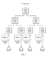
- Fig. 1 shows an example of the above concept.
- a network comprising power splitters/dividers is used to distribute the input RF signal to individual antenna elements.
- these splitters/dividers are not variable and either provide a signal or are switched off and the signal is absorbed by the resistor.
- a major drawback of this state-of-the-art approach is that by absorbing RF power rather than reflecting it, valuable RF power is wasted as heat. It would be desirable to selectively direct a signal to one or more elements of an antenna array while maintaining energy efficiency and providing flexibility.
- a first aspect of the present invention provides a feeder device for supplying a radio frequency signal to an adaptive antenna array comprising a plurality of antenna elements, said feeder device comprising: at least one signal divider, said signal divider comprising: an input port for receiving said radio frequency signal, an output port, a further output port and a variable impedance; wherein said signal divider is configured to divide said input signal and direct said divided signals towards said variable impedance; said divided signals are at least one of reflected to said output port and transmitted to said further output port, said degree of reflection and transmission depending on a value of said variable impedance; wherein said signal divider is configured such that phase shifts are introduced to signals travelling between ports, said phase shifts being such that said divided signals received at said output port and said further output port constructively interfere and signals received at outer ports of said signal divider other than said output ports are out of phase and destructively interfere; said output and said further output ports of at least one of said at least one signal divider are configured to supply signals to respective antenna elements of said antenna array.
- the inventors of the present invention recognised that the transmission and reflection of radio frequency signals are two processes that are dependent on impedance in the circuit and this dependency could be used to selectively direct a signal to one or more outputs.
- power dividers that might cause reflection of signals in antenna feeder arrays have been avoided as reflected signals can significantly reduce performance.
- the inventors recognised that the problems associated with reflection of signals in feeder networks of antenna could be mitigated where signals are divided and then recombined such that the signals interfere with each other. With a suitable selection of components and/or path lengths constructive interference between divided signals arriving at the desired outputs could be provided, while destructive interference between these signals at other outer ports could be achieved, which latter would avoid or at least reduce undesired reflected signals deteriorating performance.
- variable impedance can be used to control the degree of reflection and transmission of a signal providing a controllable, effective and low loss way of transmitting a signal to one output port, or reflecting the signal to another port, or both reflecting and transmitting different portions of the signal as desired.
- said degree of reflection and transmission is variable between substantially all reflection and substantially all transmission of said signal.
- impedance values With appropriate selection of impedance values, one may in some embodiments be able to achieve substantially complete reflection and substantially complete transmission of the signal. In this way, one or other of the output ports can be selected and the entire signal transmitted or reflected to that output port. With a choice of impedance somewhere between these two limit values, a portion of the signal can be transmitted and a portion reflected, the degree of transmission or reflection depending on the impedance value. This allows the amplitude of the signal transmitted to the multiple antenna elements to be accurately and simply controlled.
- said feeder device comprises control logic configured to control a value of said variable impedance to control said degree of reflection and transmission.
- the feeder device has control logic allowing it to control a value of the variable impedance and in this way control the degree of reflection and transmission. This allows the control logic to control the amplitude of the signal transmitted to each antenna element and this can be used to provide desired beams and allows the antenna array to be flexible and configurable.
- said at least one signal divider comprises: a directional device comprising said input port, said output port and two further ports; a further directional device comprising two ports each in data communication with a respective one of said two further ports of said directional device, and a further output port, said variable impedance being between said two further ports and said two ports; wherein said signals received at each of said two further ports are at least one of reflected to said output port of said directional device and transmitted to said further output port of said further directional device, said degree of reflection and transmission depending on a value of said variable impedance.
- the signal divider may be configured in a number of ways which make use of the reflection and transmission properties of a radio frequency signal depending on the impedance and on constructive and destructive interference to control signal amplitude, in some cases directional devices in series with each other are used with the variable impedance being located between the ports of the two devices. Changes in the variable impedance affect whether the signal is transmitted between the two devices of whether it is reflected back to the output port on the first device.
- said directional devices comprises quadrature couplers comprising four ports, direct paths between adjacent ports of said quadrature coupler introducing a phase shift of 90° to signals travelling directly between said ports.
- phase shift of 90° can be used with careful directing of the signals such that signals arriving at ports where a signal should not be output have a phased difference of 180° and as such destructively interfere, while those arriving at ports where signals are to be output have substantially no phase difference between them and as such constructively interfere.
- said directional devices comprise 3-dB couplers.
- 3-dB couplers are particularly appropriate for use as the directional devices providing the desired phase shift between input and output signals and allowing the user, with careful choice of impedance values, to select whether a signal or a particular portion of a signal is reflected and/or transmitted.
- said at least one signal divider comprises two variable impedances each of said divided signals being directed to one of said two variable impedances.
- the signal divider may require two variable impedances each of the divided signals being directed to one of them. Thus, once the signals are divided they are directed each to a separate variable impedance and are reflected and/or transmitted accordingly.
- said two variable impedances are varied in a same way to have a same impedance.
- variable impedances Although it would be possible for the two variable impedances to have different values, it may be advantageous for them to be varied in the same way such that they have a same value as this enables the signals to be matched and the destructive interference to substantially cancel out the signal arriving at the outer port where it is not desired to be output.
- said at least one signal divider comprises a fourth port, signals received from within said signal divider at said fourth port and said input port being out of phase and destructively interfering.
- the signal divider there may be a fourth port as these dividers may be symmetrical. Where this is the case, in order to avoid the requirement of an absorptive resistance to absorb the signal and avoid reflection of it, it is advantageous if the signals that arrive at the fourth port are out of phase with each other and are thereby cancelled out by destructive interference. This avoids the need for a absorptive switch and enables the signals to be recirculated rather than absorbed, increasing the energy efficiency of the device.
- the feeder device comprises a plurality of said signal dividers arranged in a cascade, said cascade comprising: an input signal divider configured to receive said radio frequency input signal and direct said signal to at least one of said output port and said further output port of said input signal divider; further signal dividers each configured to receive at an input a signal from one of said output port or said further output port of one of said signal dividers in a higher level of said cascade; and a plurality of output signal dividers each being configured to direct a received input signal via at least one of said output port and said further output port to respective antenna elements of said antenna array.
- a single signal divider may be used, it may be advantageous to have a plurality of signal dividers and these may be arranged in a cascade such that a first input signal divider receives the signal and outputs it to two further signal dividers which in turn output the signal to four outputs which may be transmitted further to four further signal dividers.
- these signal dividers may be arranged in an array such that the final row of the signal divider comprises a number of outputs that is a power of 2.
- the cascade can be formed with some signals output travelling through one number of signal dividers and other signals output travelling through a different number of signal dividers. In this way, any number of outputs can be provided.
- the amplitude of the signal transmitted to each antenna element can be controlled by controlling the varying impedances of the different signal dividers.
- said control logic is configured to independently control said variable impedance of each of said signal dividers to control signal transmitted to each of said antenna elements.
- control logic is configured to independently control the variable impedance of each of the signal dividers and thereby to control the signals transmitted to each of the transmitter elements.
- said control logic is configured to control said signals transmitted to said antenna elements such that said antenna array outputs selected beam patterns, said control logic being configured to: determine a weight of each antenna element to generate said selected beam patterns; determine values of said variable impedances required to provide a signal of a required weight to each of said antenna elements; and control said variable impedances of each of said signal dividers such that said signals of said required weight are fed by said feeder device to said antenna elements.
- the feeder network device is especially suited for configuring desired beam forms for an antenna array.
- this information is provided to the control logic which determines the weight of each antenna element of the antenna array that is required to generate such a beam pattern. Once it has determined this, it can calculate the values of the variable impedances required to provide the signals of the required weight for each of the antenna elements and thereafter, control of the variable impedances provides the desired signals to the antenna elements and the desired beam pattern is formed.
- a highly controllable adaptive array that can produce required beam patterns is provided where the input signal is recirculated about the feeder network with low dissipation allowing beams to be configured on a dynamic basis in an energy efficient fashion.
- a second aspect to the present invention provides an adaptive antenna array comprising: a plurality of antenna elements arranged in an array; a transceiver for receiving and transmitting a signal from and to said array; and a feeder device according to a first aspect of the present invention.
- a third aspect of the present invention provides a method of controlling signals transmitted via a feeder device to provide selected beam patterns at an adaptive antenna array, the feeder device comprising at least one signal divider, said signal divider comprising an input port for receiving a radio frequency signal, an output port, a further output port and a variable impedance, wherein said signal divider is configured to divide said input signal and direct said divided signals towards said variable impedance, said divided signals are at least one of reflected to said output port and transmitted to said further output port, said degree of reflection and transmission depending on a value of said variable impedance, said method comprising: determining a weight of each antenna element within said antenna array required to generate said selected beam pattern; determining values of said variable impedances within each signal divider required to provide a signal of a required weight to each of said antenna elements; and generating control signals to control said variable impedances of each of said signal dividers such that said signals of said required weight are fed by said feeder device to said antenna elements.
- aspects of the invention can be used to determine the required signals at each antenna element required to provide the desired beam pattern and to provide control signals to vary the variable impedances of the signal dividers of the feeder network to provide the required signals.
- the feeder device controlled by a method of this sort may be feeder device according to a first aspect of the present invention.
- a fourth aspect of the present invention provides a computer program operable when executed by a processor to control said processor to perform a method according to a third aspect of the present invention.
- the computer program may be part of control logic controlling the feeder device of the first aspect of the present invention.
- Embodiments seek to use the reflection and/or transmission of a radio frequency signal that may occur due to changes in impedance within the circuit, to selectively cause reflections and/or allow transmissions of a signal to cause the signal to be selectively supplied to multiple antenna elements.
- a plurality of signal dividers that direct input signals to particular or multiple outputs are used. These signal dividers recirculate the reflected signals towards outputs and thereby improve energy efficiency.
- By positioning an output in the reflected path of the signal and a further output in the transmitted path the signal can be directed towards one or other or both of the output ports, with the choice of amount of signal and output port being made by varying the impedance and thereby the degree of transmission and reflection. This is an effective and efficient way of selecting outputs which does not require an absorptive switch.
- a substantially infinite impedance causes substantially all of the radio frequency signal to be transmitted and virtually none reflected meaning the signal is output at the further output.
- a zero impedance is provided, which in effect earths the transmission line, then the signal is reflected and output at the output. Any impedance value between these two values provides some reflection and some transmission such that the signal is output at both the output and the further output.
- the output and further output are connected to antenna elements then the antenna element(s) receiving a signal can be selected.
- the splitting of the signal and the choice of phase shift between ports allows the divided signals transmitted to the output ports to be in phase providing constructive interference and increasing the energy efficiency of the device.
- Other signals transmitted towards other outer ports such as the input port are out of phase due to the design of the signal divider and destructively interfere reducing any undesired reflected signals in the system.
- signals can be directed to an outer port via different paths each path having a particular phase shift, such that the signals either constructively interfere or destructively interfere.
- the divided signals are matched destructive interference can effectively eliminate the signal removing the need for an absorptive switch.
- a distributed feeder network for RF power distribution to multiple antenna elements with reduced energy loss is disclosed.
- the performance of this network is characterized by large power division ratios, and the absence of absorptive switches.
- FIG 2 shows a feeder network comprised of a cascade of flexible non-absorptive power dividers 10 (shown in more detail in Figure 3 ) that are arranged to feed multiple antenna elements 30.
- Beam reconfiguration is achieved using the power dividers 10 by varying the admittance values of the variable impedances 20 in the network. Variation in the admittance values of the variable impedances 20 varies the amount of the signal that is reflected and the amount that is transmitted. This amount varies between substantially all or none such that the signal may be sent to a single selected one of the two outputs (port 3 and port 4 of Figure 3 ) or it may be split and portions of the signal sent to both ports. In this way, by varying the values of admittance of the variable impedances, the feeder network arrangement recirculates signals with varying amplitude and phase and provides them to selected antenna elements 30 of the antenna array providing the desired beams.
- Recirculation of input signal along the feeder network allows that which might have been dissipated in one part of the feeder network to be fed to another part of the network.
- the energy dissipated due to heat will be at a minimum or at least significantly reduced.
- the first step in the design and control of such architecture is to estimate the complex weights associated with each antenna element for a specific beam.
- the second step is to subsequently map these weights as admittance parameters for the specified architecture.
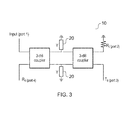
- the elementary power divider is shown in more detail in Figure 3 .
- a similar power divider has been disclosed by Bulja and Grebennikov in "A Novel Variable Power Divider with Continuous Power Division” in Microwave and Optical Technology Letters vol. 55 no. 7 pp1684 - 1686, July 2013 , however, this is in the context of supplying power to Doherty amplifiers where the problems to be addressed are the feasibility of the use high impedance lines for an asymmetric power split.
- the use of such a power divider is unique in the context of a feeder network for an antenna array.
- the input RF signal from port 1 gets split into two quadrature components, which are, depending on the value of admittance Y, either fully or partially reflected/transmitted at intermediate ports 12 and 14 towards ports 3 and 4, respectively.
- quadrature components which are, depending on the value of admittance Y, either fully or partially reflected/transmitted at intermediate ports 12 and 14 towards ports 3 and 4, respectively.
- RF power is not wasted during the division operation.
- Port 2 and port 1 by virtue of a 3-dB coupler remain isolated regardless of the value of admittance Y.
- the signal arriving at port 12 from the input port has a phase shift of 90° while that arriving at port 14 has a phase shift of 180°
- the signal reflected from port 12 to the input has an additional phase shift of 90° while that from port 14 has an additional phase shift of 180°
- the signals arriving at the input from port 12 has a phase shift of 180°
- that from port 14 has a phase shift of 360°
- the signals at the input port are therefore out of phase and the input port is protected from these reflected signals.
- the signals arriving at port 4 experience an additional 90° phase shift from port 14 and an additional 180° phase shift from port 12, thus, each signal has a phase shift of 270 when it arrives at port 4 and constructive interference occurs and the two signals combine and are output.
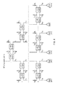
- FIG 4 shows an alternative embodiment of the proposed feeder network, where the power splitter elements are mirror images of each other. This can be advantageous when the devices are built on silicon this design making them more compact.
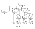
- FIG. 5 schematically shows an adaptive antenna array 50, with a feeder network 5 and control logic 40 according to an embodiment.
- Adaptive antenna array 50 comprises a plurality of antenna elements 30 supplied with signals from a network feeder array 5 comprising signal dividers 10 arranged in a cascade arrangement. Each signal divider has two outputs and one input. The outputs of the output signal dividers supply signals to respective antenna elements 30.
- Each signal divider 10 has a controllable variable impedance 20, whose impedance value is controlled by signals output by control logic 40.
- Control logic 40 is aware of the architecture of the antenna array and receives signals indicative of the beam pattern that should be output by the antenna array 50. It then calculates weights for each of the antenna elements 30 to provide the required beam pattern, from this it calculates the signals that should be supplied to each antenna element 30 to generate that beam pattern and the corresponding impedance values required at the signal splitters 10 to provide the appropriate signals to the individual antenna elements 30. It then generates and transmits control signals to control these impedances and the signals supplied to the antenna elements are appropriately weighted and the required beam pattern output.
- T s and R s are established when admittance Y is allowed to be either 0 or infinite.
- admittance Y is allowed to be either 0 or infinite.
- admittance Y can be used to control the lossless division of input power among the two output ports.
- admittance Y must be imaginary, and variable from - ⁇ to + ⁇ . This condition is well known in the design of 360° reflection type phase shifters and the principles of this design can be readily applied in the present circuit.
- the system of equations given by (7) contains 2 m equations, while the number of unknown admittances, Y m,n is equal to 2 m-1 .
- program storage devices e.g., digital data storage media, which are machine or computer readable and encode machine-executable or computer-executable programs of instructions, wherein said instructions perform some or all of the steps of said above-described methods.
- the program storage devices may be, e.g., digital memories, magnetic storage media such as a magnetic disks and magnetic tapes, hard drives, or optically readable digital data storage media.
- the embodiments are also intended to cover computers programmed to perform said steps of the above-described methods.
- processors may be provided through the use of dedicated hardware as well as hardware capable of executing software in association with appropriate software.
- the functions may be provided by a single dedicated processor, by a single shared processor, or by a plurality of individual processors, some of which may be shared.
- processor or “controller” or “logic” should not be construed to refer exclusively to hardware capable of executing software, and may implicitly include, without limitation, digital signal processor (DSP) hardware, network processor, application specific integrated circuit (ASIC), field programmable gate array (FPGA), read only memory (ROM) for storing software, random access memory (RAM), and non-volatile storage. Other hardware, conventional and/or custom, may also be included.
- DSP digital signal processor
- ASIC application specific integrated circuit
- FPGA field programmable gate array
- ROM read only memory
- RAM random access memory
- non-volatile storage Other hardware, conventional and/or custom, may also be included.
- any switches shown in the Figures are conceptual only. Their function may be carried out through the operation of program logic, through dedicated logic, through the interaction of program control and dedicated logic, or even manually, the particular technique being selectable by the implementer as more specifically understood from the context.
- any block diagrams herein represent conceptual views of illustrative circuitry embodying the principles of the invention.
- any flow charts, flow diagrams, state transition diagrams, pseudo code, and the like represent various processes which may be substantially represented in computer readable medium and so executed by a computer or processor, whether or not such computer or processor is explicitly shown.
Landscapes
- Variable-Direction Aerials And Aerial Arrays (AREA)
Abstract
Description
- The present invention relates to feeding signals to adaptive antenna arrays and to those adaptive antenna arrays.
- Antenna arrays have been widely used in telecommunications, due to their ability to: focus RF signals towards a specific sector and to utilize MIMO techniques to improve coverage and capacity.
- In many beamforming/MIMO applications, it is advantageous if the antenna/antenna array can be reconfigurable so that not only can it provide a narrow-beam of RF power to a particular user or a particular set of users, but it also can provide a wide RF coverage to a larger number of users.
- Adaptive beam configuration/forming can be accomplished either in the RF domain or in the digital domain. Digital approaches offer full flexibility however at increased cost and energy consumption. Alternatively, adaptive beam reconfiguration in RF can be achieved by, say switching on or off selected antenna elements depending on the beam required. In this case by switching elements off an array is provided that operates with reduced elements resulting in a wider beam at the cost of reduced power along the main beam. This can extend to the case where all but one antenna element is switched off, resulting in the maximum angular coverage while limiting the range along the radial direction. One limitation with such an approach is that, turning antenna elements off is usually implemented using an absorptive switch which reduces energy efficiency since power is dissipated in the feeder network in the form of heat.
- The reason that such absorption mechanisms are generally used is that any RF power reflection significantly deteriorates the performance of the overall system. For example, RF power reflection is particularly detrimental for an RF Power Amplifier and may cause it to exhibit unstable behaviour which could lead to a complete system break-down.
-
Fig. 1 shows an example of the above concept. In this example, a network comprising power splitters/dividers is used to distribute the input RF signal to individual antenna elements. Generally these splitters/dividers are not variable and either provide a signal or are switched off and the signal is absorbed by the resistor. - Obtaining a large power division ratio at a power splitter is not a simple task and owing to this and problems that arise in such systems where reflected signals are transmitted back towards the input, a solution has generally been used that uses an absorptive switch added at the output of the power distribution network with the aim of selectively disabling the signal feed to a particular antenna element and avoiding reflections of the signal.
- A major drawback of this state-of-the-art approach is that by absorbing RF power rather than reflecting it, valuable RF power is wasted as heat. It would be desirable to selectively direct a signal to one or more elements of an antenna array while maintaining energy efficiency and providing flexibility.
- A first aspect of the present invention provides a feeder device for supplying a radio frequency signal to an adaptive antenna array comprising a plurality of antenna elements, said feeder device comprising: at least one signal divider, said signal divider comprising: an input port for receiving said radio frequency signal, an output port, a further output port and a variable impedance; wherein said signal divider is configured to divide said input signal and direct said divided signals towards said variable impedance; said divided signals are at least one of reflected to said output port and transmitted to said further output port, said degree of reflection and transmission depending on a value of said variable impedance; wherein said signal divider is configured such that phase shifts are introduced to signals travelling between ports, said phase shifts being such that said divided signals received at said output port and said further output port constructively interfere and signals received at outer ports of said signal divider other than said output ports are out of phase and destructively interfere; said output and said further output ports of at least one of said at least one signal divider are configured to supply signals to respective antenna elements of said antenna array.
- The inventors of the present invention recognised that the transmission and reflection of radio frequency signals are two processes that are dependent on impedance in the circuit and this dependency could be used to selectively direct a signal to one or more outputs. In general power dividers that might cause reflection of signals in antenna feeder arrays have been avoided as reflected signals can significantly reduce performance. However, the inventors recognised that the problems associated with reflection of signals in feeder networks of antenna could be mitigated where signals are divided and then recombined such that the signals interfere with each other. With a suitable selection of components and/or path lengths constructive interference between divided signals arriving at the desired outputs could be provided, while destructive interference between these signals at other outer ports could be achieved, which latter would avoid or at least reduce undesired reflected signals deteriorating performance.
- In this way, a variable impedance can be used to control the degree of reflection and transmission of a signal providing a controllable, effective and low loss way of transmitting a signal to one output port, or reflecting the signal to another port, or both reflecting and transmitting different portions of the signal as desired.
- Although in some cases the degree of reflection and transmission might be bounded, in some embodiments, said degree of reflection and transmission is variable between substantially all reflection and substantially all transmission of said signal.
- With appropriate selection of impedance values, one may in some embodiments be able to achieve substantially complete reflection and substantially complete transmission of the signal. In this way, one or other of the output ports can be selected and the entire signal transmitted or reflected to that output port. With a choice of impedance somewhere between these two limit values, a portion of the signal can be transmitted and a portion reflected, the degree of transmission or reflection depending on the impedance value. This allows the amplitude of the signal transmitted to the multiple antenna elements to be accurately and simply controlled.
- In some embodiments, said feeder device comprises control logic configured to control a value of said variable impedance to control said degree of reflection and transmission.
- Given the controllable nature of the at least one signal divider, it may be advantageous if the feeder device has control logic allowing it to control a value of the variable impedance and in this way control the degree of reflection and transmission. This allows the control logic to control the amplitude of the signal transmitted to each antenna element and this can be used to provide desired beams and allows the antenna array to be flexible and configurable.
- In some embodiments, said at least one signal divider comprises: a directional device comprising said input port, said output port and two further ports; a further directional device comprising two ports each in data communication with a respective one of said two further ports of said directional device, and a further output port, said variable impedance being between said two further ports and said two ports; wherein said signals received at each of said two further ports are at least one of reflected to said output port of said directional device and transmitted to said further output port of said further directional device, said degree of reflection and transmission depending on a value of said variable impedance.
- Although the signal divider may be configured in a number of ways which make use of the reflection and transmission properties of a radio frequency signal depending on the impedance and on constructive and destructive interference to control signal amplitude, in some cases directional devices in series with each other are used with the variable impedance being located between the ports of the two devices. Changes in the variable impedance affect whether the signal is transmitted between the two devices of whether it is reflected back to the output port on the first device.
- In some embodiments, said directional devices comprises quadrature couplers comprising four ports, direct paths between adjacent ports of said quadrature coupler introducing a phase shift of 90° to signals travelling directly between said ports.
- One way in which the signal divider could be implemented is by the use of quadrature couplers which have four ports with direct paths between adjacent ports introducing a phase shift of 90°. This phase shift of 90° can be used with careful directing of the signals such that signals arriving at ports where a signal should not be output have a phased difference of 180° and as such destructively interfere, while those arriving at ports where signals are to be output have substantially no phase difference between them and as such constructively interfere.
- In some embodiments, said directional devices comprise 3-dB couplers.
- 3-dB couplers are particularly appropriate for use as the directional devices providing the desired phase shift between input and output signals and allowing the user, with careful choice of impedance values, to select whether a signal or a particular portion of a signal is reflected and/or transmitted.
- In some embodiments, said at least one signal divider comprises two variable impedances each of said divided signals being directed to one of said two variable impedances.
- The signal divider may require two variable impedances each of the divided signals being directed to one of them. Thus, once the signals are divided they are directed each to a separate variable impedance and are reflected and/or transmitted accordingly.
- In some embodiments, said two variable impedances are varied in a same way to have a same impedance.
- Although it would be possible for the two variable impedances to have different values, it may be advantageous for them to be varied in the same way such that they have a same value as this enables the signals to be matched and the destructive interference to substantially cancel out the signal arriving at the outer port where it is not desired to be output.
- In some embodiments, said at least one signal divider comprises a fourth port, signals received from within said signal divider at said fourth port and said input port being out of phase and destructively interfering.
- In many implementations of the signal divider there may be a fourth port as these dividers may be symmetrical. Where this is the case, in order to avoid the requirement of an absorptive resistance to absorb the signal and avoid reflection of it, it is advantageous if the signals that arrive at the fourth port are out of phase with each other and are thereby cancelled out by destructive interference. This avoids the need for a absorptive switch and enables the signals to be recirculated rather than absorbed, increasing the energy efficiency of the device.
- In some embodiments, the feeder device comprises a plurality of said signal dividers arranged in a cascade, said cascade comprising: an input signal divider configured to receive said radio frequency input signal and direct said signal to at least one of said output port and said further output port of said input signal divider; further signal dividers each configured to receive at an input a signal from one of said output port or said further output port of one of said signal dividers in a higher level of said cascade; and a plurality of output signal dividers each being configured to direct a received input signal via at least one of said output port and said further output port to respective antenna elements of said antenna array.
- Although when feeding just two antenna elements a single signal divider may be used, it may be advantageous to have a plurality of signal dividers and these may be arranged in a cascade such that a first input signal divider receives the signal and outputs it to two further signal dividers which in turn output the signal to four outputs which may be transmitted further to four further signal dividers. In some cases, these signal dividers may be arranged in an array such that the final row of the signal divider comprises a number of outputs that is a power of 2. However, where a different number of antenna elements is desired, then the cascade can be formed with some signals output travelling through one number of signal dividers and other signals output travelling through a different number of signal dividers. In this way, any number of outputs can be provided. Furthermore, the amplitude of the signal transmitted to each antenna element can be controlled by controlling the varying impedances of the different signal dividers.
- In some embodiments, said control logic is configured to independently control said variable impedance of each of said signal dividers to control signal transmitted to each of said antenna elements.
- Where there are multiple signal dividers, advantageously the control logic is configured to independently control the variable impedance of each of the signal dividers and thereby to control the signals transmitted to each of the transmitter elements.
- In some embodiments, said control logic is configured to control said signals transmitted to said antenna elements such that said antenna array outputs selected beam patterns, said control logic being configured to: determine a weight of each antenna element to generate said selected beam patterns; determine values of said variable impedances required to provide a signal of a required weight to each of said antenna elements; and control said variable impedances of each of said signal dividers such that said signals of said required weight are fed by said feeder device to said antenna elements.
- The feeder network device is especially suited for configuring desired beam forms for an antenna array. In this regard, when certain beam patterns are required, this information is provided to the control logic which determines the weight of each antenna element of the antenna array that is required to generate such a beam pattern. Once it has determined this, it can calculate the values of the variable impedances required to provide the signals of the required weight for each of the antenna elements and thereafter, control of the variable impedances provides the desired signals to the antenna elements and the desired beam pattern is formed. Thus, a highly controllable adaptive array that can produce required beam patterns is provided where the input signal is recirculated about the feeder network with low dissipation allowing beams to be configured on a dynamic basis in an energy efficient fashion.
- A second aspect to the present invention provides an adaptive antenna array comprising: a plurality of antenna elements arranged in an array; a transceiver for receiving and transmitting a signal from and to said array; and a feeder device according to a first aspect of the present invention.
- A third aspect of the present invention provides a method of controlling signals transmitted via a feeder device to provide selected beam patterns at an adaptive antenna array, the feeder device comprising at least one signal divider, said signal divider comprising an input port for receiving a radio frequency signal, an output port, a further output port and a variable impedance, wherein said signal divider is configured to divide said input signal and direct said divided signals towards said variable impedance, said divided signals are at least one of reflected to said output port and transmitted to said further output port, said degree of reflection and transmission depending on a value of said variable impedance, said method comprising: determining a weight of each antenna element within said antenna array required to generate said selected beam pattern; determining values of said variable impedances within each signal divider required to provide a signal of a required weight to each of said antenna elements; and generating control signals to control said variable impedances of each of said signal dividers such that said signals of said required weight are fed by said feeder device to said antenna elements.
- Aspects of the invention can be used to determine the required signals at each antenna element required to provide the desired beam pattern and to provide control signals to vary the variable impedances of the signal dividers of the feeder network to provide the required signals. The feeder device controlled by a method of this sort may be feeder device according to a first aspect of the present invention.
- A fourth aspect of the present invention provides a computer program operable when executed by a processor to control said processor to perform a method according to a third aspect of the present invention.
- In some embodiments the computer program may be part of control logic controlling the feeder device of the first aspect of the present invention.
- Further particular and preferred aspects are set out in the accompanying independent and dependent claims. Features of the dependent claims may be combined with features of the independent claims as appropriate, and in combinations other than those explicitly set out in the claims.
- Where an apparatus feature is described as being operable to provide a function, it will be appreciated that this includes an apparatus feature which provides that function or which is adapted or configured to provide that function.
- Embodiments of the present invention will now be described further, with reference to the accompanying drawings, in which:
-
Figure 1 illustrates an array of four switched antenna elements according to the prior art; -
Figure 2 shows a feeder circuit for an antenna array according to an embodiment; -
Figure 3 shows a signal divider for use in an embodiment; -
Figure 4 shows a feeder circuit according to a further embodiment; and -
Figure 5 shows an adaptive antenna array, feeder network and control circuitry according to an embodiment. - Before discussing the embodiments in any more detail, first an overview will be provided.
- Embodiments seek to use the reflection and/or transmission of a radio frequency signal that may occur due to changes in impedance within the circuit, to selectively cause reflections and/or allow transmissions of a signal to cause the signal to be selectively supplied to multiple antenna elements. A plurality of signal dividers that direct input signals to particular or multiple outputs are used. These signal dividers recirculate the reflected signals towards outputs and thereby improve energy efficiency. By positioning an output in the reflected path of the signal and a further output in the transmitted path the signal can be directed towards one or other or both of the output ports, with the choice of amount of signal and output port being made by varying the impedance and thereby the degree of transmission and reflection. This is an effective and efficient way of selecting outputs which does not require an absorptive switch.
- Where the impedance is in parallel with the transmission line, then a substantially infinite impedance causes substantially all of the radio frequency signal to be transmitted and virtually none reflected meaning the signal is output at the further output. Where a zero impedance is provided, which in effect earths the transmission line, then the signal is reflected and output at the output. Any impedance value between these two values provides some reflection and some transmission such that the signal is output at both the output and the further output. Where the output and further output are connected to antenna elements then the antenna element(s) receiving a signal can be selected.
- Furthermore, the splitting of the signal and the choice of phase shift between ports allows the divided signals transmitted to the output ports to be in phase providing constructive interference and increasing the energy efficiency of the device. Other signals transmitted towards other outer ports such as the input port are out of phase due to the design of the signal divider and destructively interfere reducing any undesired reflected signals in the system.
- In effect by providing paths with different phase shifts between elements and directing divided signals appropriately, signals can be directed to an outer port via different paths each path having a particular phase shift, such that the signals either constructively interfere or destructively interfere. Where the divided signals are matched destructive interference can effectively eliminate the signal removing the need for an absorptive switch.
- In effect, a lossless or at least reduced loss and cost effective solution for adaptive beam reconfiguration in RF is proposed.
- In particular, a distributed feeder network for RF power distribution to multiple antenna elements with reduced energy loss is disclosed. The performance of this network is characterized by large power division ratios, and the absence of absorptive switches.
-
Figure 2 shows a feeder network comprised of a cascade of flexible non-absorptive power dividers 10 (shown in more detail inFigure 3 ) that are arranged to feedmultiple antenna elements 30. Beam reconfiguration is achieved using thepower dividers 10 by varying the admittance values of thevariable impedances 20 in the network. Variation in the admittance values of thevariable impedances 20 varies the amount of the signal that is reflected and the amount that is transmitted. This amount varies between substantially all or none such that the signal may be sent to a single selected one of the two outputs (port 3 andport 4 ofFigure 3 ) or it may be split and portions of the signal sent to both ports. In this way, by varying the values of admittance of the variable impedances, the feeder network arrangement recirculates signals with varying amplitude and phase and provides them to selectedantenna elements 30 of the antenna array providing the desired beams. - Recirculation of input signal along the feeder network allows that which might have been dissipated in one part of the feeder network to be fed to another part of the network. Thus, as the beams are configured on a dynamic basis, the energy dissipated due to heat will be at a minimum or at least significantly reduced.
- The first step in the design and control of such architecture is to estimate the complex weights associated with each antenna element for a specific beam. The second step is to subsequently map these weights as admittance parameters for the specified architecture.
- Consider
Fig. 2 with N = 2^m + 1 antennas, the amplitude and phase weights can be designed to produce a main lobe along direction θ while minimizing or at least reducing the energy radiated across all other directions
- u(θ) amplitude and phase weights for a given beam
- α(θ) array response for given angle
- Rα is the overall array response
- One approach to obtain the optimal solution for (1.0) is through Lagrange multiplier approach. Proceeding along the same lines, we can explicitly represent the admittance parameters of the feeder network as a function of u(θ) and solve for these parameters. Such an optimization ensures that the feeder network circuitry is optimized or at least improved to reduce loss and obtain desired beam pattern performance. One example of such a design is explained below.
- The elementary power divider is shown in more detail in
Figure 3 . A similar power divider has been disclosed by Bulja and Grebennikov in "A Novel Variable Power Divider with Continuous Power Division" in Microwave and Optical Technology Letters vol. 55 no. 7 pp1684 - 1686, July 2013, however, this is in the context of supplying power to Doherty amplifiers where the problems to be addressed are the feasibility of the use high impedance lines for an asymmetric power split. In this regard, the use of such a power divider is unique in the context of a feeder network for an antenna array. The advantages of such a power divider in an antenna feeder array is that no or at least very low RF power is dissipated in the termination resistor, Rt, and that the input RF power atport 1 can be, varied depending on the value of admittance Y, and can be either fully reflected towardsport 4 of fully transmitted toport 3. - The principle of operation of the power splitter of
Figure 3 is described next. The input RF signal fromport 1 gets split into two quadrature components, which are, depending on the value of admittance Y, either fully or partially reflected/transmitted at intermediate ports 12 and 14 towardsports Port 2 andport 1, by virtue of a 3-dB coupler remain isolated regardless of the value of admittance Y. - In this regard the signal arriving at port 12 from the input port has a phase shift of 90° while that arriving at port 14 has a phase shift of 180°, when reflected at ports 12 and 14, the signal reflected from port 12 to the input has an additional phase shift of 90° while that from port 14 has an additional phase shift of 180°, thus, the signals arriving at the input from port 12 has a phase shift of 180°, while that from port 14 has a phase shift of 360°, the signals at the input port are therefore out of phase and the input port is protected from these reflected signals. The signals arriving at
port 4 by contrast, experience an additional 90° phase shift from port 14 and an additional 180° phase shift from port 12, thus, each signal has a phase shift of 270 when it arrives atport 4 and constructive interference occurs and the two signals combine and are output. - Similar phase changes occur with signals transmitted through the second 3-dB coupler such that destructive interference occurs at
port 2 and constructive interference atport 3. - Now, by utilizing the circuit of
Fig. 3 as a constitutive, unit power divider cell of the antenna feeder network it is possible to obtain almost any power division of the input RF signal. In particular, this means: - The input RF signal can be split in almost any power division ratio - the limit case lies with switching some antenna elements fully off.
- There will be no or minimal loss of RF power in case of switching off desired antenna elements. In this case, RF power will be re-distributed among the remaining "switched on" antenna elements.
-
Figure 4 shows an alternative embodiment of the proposed feeder network, where the power splitter elements are mirror images of each other. This can be advantageous when the devices are built on silicon this design making them more compact. -
Figure 5 schematically shows an adaptive antenna array 50, with afeeder network 5 and controllogic 40 according to an embodiment. Adaptive antenna array 50 comprises a plurality ofantenna elements 30 supplied with signals from anetwork feeder array 5 comprisingsignal dividers 10 arranged in a cascade arrangement. Each signal divider has two outputs and one input. The outputs of the output signal dividers supply signals torespective antenna elements 30. - Each
signal divider 10 has a controllablevariable impedance 20, whose impedance value is controlled by signals output bycontrol logic 40.Control logic 40 is aware of the architecture of the antenna array and receives signals indicative of the beam pattern that should be output by the antenna array 50. It then calculates weights for each of theantenna elements 30 to provide the required beam pattern, from this it calculates the signals that should be supplied to eachantenna element 30 to generate that beam pattern and the corresponding impedance values required at thesignal splitters 10 to provide the appropriate signals to theindividual antenna elements 30. It then generates and transmits control signals to control these impedances and the signals supplied to the antenna elements are appropriately weighted and the required beam pattern output. - The S-parameter matrix of the circuit of
Fig. 3 are

- In (2) and (3), T s and R s represent the transmission and reflection coefficients, while Z o is the characteristic impedance of the interconnecting transmission line. It can be shown that, if the admittance Y of the varactor diode is purely imaginary, the power conservation condition is satisfied, i.e.

- The two ultimate cases for T s and R s are established when admittance Y is allowed to be either 0 or infinite. For the case when Y = 0, (2) and (3) become


- The transmission coefficients for the antenna elements, denoted from 0 to 2m-1 are


- The system of equations given by (7) contains 2m equations, while the number of unknown admittances, Ym,n is equal to 2m-1. However, the system of 2m equations given by (7) is not linearly independent and the antenna outputs given by (7) need to satisfy a power conservation principle, i.e.

- The last term in (8) denotes the loss contribution of the overall system, which is usually known. Now, (7) and (8) form a linearly independent system of 2m-1 equations, which can be uniquely solved for Ym,n. The solutions for Ym,n will ultimately depend on the required division of power among the antenna ports.
- A person of skill in the art would readily recognize that steps of various above-described methods can be performed by programmed computers. Herein, some embodiments are also intended to cover program storage devices, e.g., digital data storage media, which are machine or computer readable and encode machine-executable or computer-executable programs of instructions, wherein said instructions perform some or all of the steps of said above-described methods. The program storage devices may be, e.g., digital memories, magnetic storage media such as a magnetic disks and magnetic tapes, hard drives, or optically readable digital data storage media. The embodiments are also intended to cover computers programmed to perform said steps of the above-described methods.
- The functions of the various elements shown in the Figures, including any functional blocks labelled as "processors" or "logic", may be provided through the use of dedicated hardware as well as hardware capable of executing software in association with appropriate software. When provided by a processor, the functions may be provided by a single dedicated processor, by a single shared processor, or by a plurality of individual processors, some of which may be shared. Moreover, explicit use of the term "processor" or "controller" or "logic" should not be construed to refer exclusively to hardware capable of executing software, and may implicitly include, without limitation, digital signal processor (DSP) hardware, network processor, application specific integrated circuit (ASIC), field programmable gate array (FPGA), read only memory (ROM) for storing software, random access memory (RAM), and non-volatile storage. Other hardware, conventional and/or custom, may also be included. Similarly, any switches shown in the Figures are conceptual only. Their function may be carried out through the operation of program logic, through dedicated logic, through the interaction of program control and dedicated logic, or even manually, the particular technique being selectable by the implementer as more specifically understood from the context.
- It should be appreciated by those skilled in the art that any block diagrams herein represent conceptual views of illustrative circuitry embodying the principles of the invention. Similarly, it will be appreciated that any flow charts, flow diagrams, state transition diagrams, pseudo code, and the like represent various processes which may be substantially represented in computer readable medium and so executed by a computer or processor, whether or not such computer or processor is explicitly shown.
- The description and drawings merely illustrate the principles of the invention. It will thus be appreciated that those skilled in the art will be able to devise various arrangements that, although not explicitly described or shown herein, embody the principles of the invention and are included within its spirit and scope. Furthermore, all examples recited herein are principally intended expressly to be only for pedagogical purposes to aid the reader in understanding the principles of the invention and the concepts contributed by the inventor(s) to furthering the art, and are to be construed as being without limitation to such specifically recited examples and conditions. Moreover, all statements herein reciting principles, aspects, and embodiments of the invention, as well as specific examples thereof, are intended to encompass equivalents thereof.
Claims (15)
- A feeder device for supplying a radio frequency signal to an adaptive antenna array comprising a plurality of antenna elements, said feeder device comprising:at least one signal divider, said signal divider comprising:an input port for receiving said radio frequency signal, an output port, a further output port and a variable impedance; whereinsaid signal divider is configured to divide said input signal and direct said divided signals towards said variable impedance;said divided signals are at least one of reflected to said output port and transmitted to said further output port, said degree of reflection and transmission depending on a value of said variable impedance; whereinsaid signal divider is configured such that phase shifts are introduced to signals travelling between ports, said phase shifts being such that said divided signals received at said output port and said further output port constructively interfere and signals received at outer ports of said signal divider other than said output ports are out of phase and destructively interfere;said output and said further output ports of at least one of said at least one signal divider are configured to supply signals to respective antenna elements of said antenna array.
- A device according to claim 1, wherein said degree of reflection and transmission is variable between substantially all reflection and substantially all transmission of said signal.
- A feeder device according to any preceding claim, said feeder device comprising control logic configured to control a value of said variable impedance to control said degree of reflection and transmission.
- A feeder device according to any preceding claim, wherein said at least one signal divider comprises:a directional device comprising said input port, said output port and two further ports;a further directional device comprising two ports each in data communication with a respective one of said two further ports of said directional device, and a further output port, said variable impedance being between said two further ports and said two ports; whereinsaid signals received at each of said two further ports are at least one of reflected to said output port of said directional device and transmitted to said further output port of said further directional device, said degree of reflection and transmission depending on a value of said variable impedance.
- A feeder device according to claim 4, wherein said directional devices comprises quadrature couplers comprising four ports, direct paths between adjacent ports of said quadrature coupler introducing a phase shift of 90° to signals travelling directly between said ports.
- A feeder device according to claim 4 or 5, wherein said directional devices comprise 3-dB couplers.
- A feeder device according to any preceding claim, wherein said at least one signal divider comprises two variable impedances each of said divided signals being directed to one of said two variable impedances.
- A feeder device according to claim 7, wherein said two variable impedances are varied in a same way to have a same impedance.
- A feeder device according to any preceding claim, wherein said at least one signal divider comprises a fourth port, signals received from within said signal divider at said fourth port and said input port being out of phase and destructively interfering.
- A feeder device according to any preceding claim, comprising a plurality of said signal dividers arranged in a cascade, said cascade comprising:an input signal divider configured to receive said radio frequency input signal and direct said signal to at least one of said output port and said further output port of said input signal divider;further signal dividers each configured to receive at an input a signal from one of said output port or said further output port of one of said signal dividers in a higher level of said cascade; anda plurality of output signal dividers each being configured to direct a received input signal via at at least one of said output port and said further output port to respective antenna elements of said antenna array.
- A feeder device according to claim 10 and claim 3, wherein said control logic is configured to independently control said variable impedance of each of said signal dividers to control signals transmitted to each of said antenna elements.
- A feeder device according to claim 11, wherein said control logic is configured to control an amplitude of said signals transmitted to each of said multiple antenna elements such that said antenna array outputs selected beam patterns, said control logic being configured to:determine a weight of each antenna element to generate said selected beam patterns;determine values of said variable impedance required to provide a signal of a required weight to each of said antenna elements; andcontrol said variable impedances of each of said signal dividers such that said signals of said required weight are fed by said feeder device to said antenna elements.
- An adaptive antenna array comprising:a plurality of antenna elements arranged in an array;a transceiver for receiving and transmitting a signal from and to said antenna array; anda feeder device according to any preceding claim.
- A method of controlling signals transmitted via a feeder device to provide selected beam patterns at an adaptive antenna array, the feeder device comprising at least one signal divider, said signal divider comprising an input port for receiving a radio frequency signal, an output port, a further output port and a variable impedance, wherein said signal divider is configured to divide said input signal and direct said divided signals towards said variable impedance, said divided signals are at least one of reflected to said output port and transmitted to said further output port, said degree of reflection and transmission depending on a value of said variable impedance, said method comprising:determining a weight of each antenna element within said antenna array required to generate said selected beam pattern;determining values of said variable impedances within each signal divider required to provide a signal of a required weight to each of said antenna elements; andgenerating control signals to control said variable impedances of each of said signal dividers such that said signals of said required weight are fed by said feeder device to said antenna elements.
- A computer program operable when executed by a processor is operable to control said processor to perform a method according to claim 14.
Priority Applications (2)
| Application Number | Priority Date | Filing Date | Title |
|---|---|---|---|
| EP15306264.1A EP3128612B1 (en) | 2015-08-04 | 2015-08-04 | An adaptive antenna array and an apparatus and method for feeding signals to an adaptive antenna array |
| ES15306264T ES2842108T3 (en) | 2015-08-04 | 2015-08-04 | An adaptive antenna array and an apparatus and method for feeding signals to an adaptive antenna array |
Applications Claiming Priority (1)
| Application Number | Priority Date | Filing Date | Title |
|---|---|---|---|
| EP15306264.1A EP3128612B1 (en) | 2015-08-04 | 2015-08-04 | An adaptive antenna array and an apparatus and method for feeding signals to an adaptive antenna array |
Publications (2)
| Publication Number | Publication Date |
|---|---|
| EP3128612A1 true EP3128612A1 (en) | 2017-02-08 |
| EP3128612B1 EP3128612B1 (en) | 2020-11-18 |
Family
ID=53800920
Family Applications (1)
| Application Number | Title | Priority Date | Filing Date |
|---|---|---|---|
| EP15306264.1A Active EP3128612B1 (en) | 2015-08-04 | 2015-08-04 | An adaptive antenna array and an apparatus and method for feeding signals to an adaptive antenna array |
Country Status (2)
| Country | Link |
|---|---|
| EP (1) | EP3128612B1 (en) |
| ES (1) | ES2842108T3 (en) |
Cited By (2)
| Publication number | Priority date | Publication date | Assignee | Title |
|---|---|---|---|---|
| CN111432724A (en) * | 2017-10-05 | 2020-07-17 | 美国贝鲁特大学 | Novel non-invasive biological, chemical marker and tracer monitoring device for monitoring blood containing glucose using adaptive radio frequency circuit and antenna design |
| US11811124B2 (en) | 2020-10-22 | 2023-11-07 | Nokia Technologies Oy | Controllable radio frequency switching and/or splitting device |
Citations (5)
| Publication number | Priority date | Publication date | Assignee | Title |
|---|---|---|---|---|
| WO2004038452A1 (en) * | 2002-10-24 | 2004-05-06 | Telefonaktiebolaget Lm Ericsson | Adaptive antenna |
| US20050270123A1 (en) * | 2001-01-31 | 2005-12-08 | Ipr Licensing, Inc. | Electronic phase reflector with enhanced phase shift performance |
| EP1642357A1 (en) * | 2003-05-17 | 2006-04-05 | Quintel Technology Limited | Phased array antenna system with adjustable electrical tilt |
| EP2538578A2 (en) * | 2012-04-20 | 2012-12-26 | Huawei Technologies Co., Ltd. | Antenna, base station and beam processing method |
| EP2698870A1 (en) * | 2012-08-14 | 2014-02-19 | Alcatel-Lucent | Antenna feed |
-
2015
- 2015-08-04 ES ES15306264T patent/ES2842108T3/en active Active
- 2015-08-04 EP EP15306264.1A patent/EP3128612B1/en active Active
Patent Citations (5)
| Publication number | Priority date | Publication date | Assignee | Title |
|---|---|---|---|---|
| US20050270123A1 (en) * | 2001-01-31 | 2005-12-08 | Ipr Licensing, Inc. | Electronic phase reflector with enhanced phase shift performance |
| WO2004038452A1 (en) * | 2002-10-24 | 2004-05-06 | Telefonaktiebolaget Lm Ericsson | Adaptive antenna |
| EP1642357A1 (en) * | 2003-05-17 | 2006-04-05 | Quintel Technology Limited | Phased array antenna system with adjustable electrical tilt |
| EP2538578A2 (en) * | 2012-04-20 | 2012-12-26 | Huawei Technologies Co., Ltd. | Antenna, base station and beam processing method |
| EP2698870A1 (en) * | 2012-08-14 | 2014-02-19 | Alcatel-Lucent | Antenna feed |
Non-Patent Citations (2)
| Title |
|---|
| BULJA; GREBENNIKOV: "A Novel Variable Power Divider with Continuous Power Division", MICROWAVE AND OPTICAL TECHNOLOGY LETTERS, vol. 55, no. 7, July 2013 (2013-07-01), pages 1684 - 1686, XP055150809, DOI: doi:10.1002/mop.27603 |
| SENAD BULJA ET AL: "A novel variable power divider with continuous power division", MICROWAVE AND OPTICAL TECHNOLOGY LETTERS, vol. 55, no. 7, 26 April 2013 (2013-04-26), pages 1684 - 1686, XP055150809, ISSN: 0895-2477, DOI: 10.1002/mop.27603 * |
Cited By (3)
| Publication number | Priority date | Publication date | Assignee | Title |
|---|---|---|---|---|
| CN111432724A (en) * | 2017-10-05 | 2020-07-17 | 美国贝鲁特大学 | Novel non-invasive biological, chemical marker and tracer monitoring device for monitoring blood containing glucose using adaptive radio frequency circuit and antenna design |
| CN111432724B (en) * | 2017-10-05 | 2024-11-12 | 美国贝鲁特大学 | Non-invasive biomarker and tracer monitoring device using adaptive radiofrequency circuits |
| US11811124B2 (en) | 2020-10-22 | 2023-11-07 | Nokia Technologies Oy | Controllable radio frequency switching and/or splitting device |
Also Published As
| Publication number | Publication date |
|---|---|
| ES2842108T3 (en) | 2021-07-12 |
| EP3128612B1 (en) | 2020-11-18 |
Similar Documents
| Publication | Publication Date | Title |
|---|---|---|
| KR102804543B1 (en) | System and method for multibeam beamforming front-end architecture for wireless transceiver | |
| US10171141B2 (en) | Hybrid beam-forming antenna array using selection matrix for antenna phase calibration | |
| WO2018177142A1 (en) | Antenna system, signal processing system and signal processing method | |
| US20150288438A1 (en) | Modular antenna array with rf and baseband beamforming | |
| US11728858B1 (en) | Element-level self-calculation of phased array vectors using interpolation | |
| EP3675280B1 (en) | Switched-beam communication node | |
| EP3419104B1 (en) | Cellular communication systems having antenna arrays therein with enhanced half power beam width (hpbw) control | |
| US11189911B2 (en) | Compact combiner for phased-array antenna beamformer | |
| US20140357319A1 (en) | Beamforming system and method for modular phased antenna array | |
| US8730104B2 (en) | Programmable wide-band radio frequency feed network | |
| JP7604113B2 (en) | High-speed spatial searching using phased array antennas | |
| US11205858B1 (en) | Element-level self-calculation of phased array vectors using direct calculation | |
| US10498415B2 (en) | Systems and methods for a multi-mode active electronically scanned array | |
| EP3128612B1 (en) | An adaptive antenna array and an apparatus and method for feeding signals to an adaptive antenna array | |
| WO2024037229A1 (en) | Phase shift matrix circuit, beamforming circuit, phase shift method, device, and system | |
| CN105680178A (en) | Two-dimensional electronic scanning antenna | |
| CN119199760B (en) | A phased array radar jammer system with multi-beam reception and narrow beam transmission | |
| US20250141100A1 (en) | Phased array antenna with reconfigurable time delay units and associated methods | |
| US10020578B2 (en) | Antenna arrangement with variable antenna pattern | |
| US20250030466A1 (en) | Configurable beamformer integrated circuit control | |
| CA3085599A1 (en) | Multiscale vector constellation | |
| CA2899771A1 (en) | Systems and methods for high power microwave combining and switching | |
| US20260066536A1 (en) | Switched Splitter-Combiner for Local Excitation of Wideband Antenna Arrays | |
| KR102950314B1 (en) | Apparatus and method for high frequency phase shifter | |
| CN115494459B (en) | Polarization reconfigurable is an electron reflector of (a) |
Legal Events
| Date | Code | Title | Description |
|---|---|---|---|
| PUAI | Public reference made under article 153(3) epc to a published international application that has entered the european phase |
Free format text: ORIGINAL CODE: 0009012 |
|
| STAA | Information on the status of an ep patent application or granted ep patent |
Free format text: STATUS: THE APPLICATION HAS BEEN PUBLISHED |
|
| AK | Designated contracting states |
Kind code of ref document: A1 Designated state(s): AL AT BE BG CH CY CZ DE DK EE ES FI FR GB GR HR HU IE IS IT LI LT LU LV MC MK MT NL NO PL PT RO RS SE SI SK SM TR |
|
| AX | Request for extension of the european patent |
Extension state: BA ME |
|
| STAA | Information on the status of an ep patent application or granted ep patent |
Free format text: STATUS: REQUEST FOR EXAMINATION WAS MADE |
|
| 17P | Request for examination filed |
Effective date: 20170808 |
|
| RBV | Designated contracting states (corrected) |
Designated state(s): AL AT BE BG CH CY CZ DE DK EE ES FI FR GB GR HR HU IE IS IT LI LT LU LV MC MK MT NL NO PL PT RO RS SE SI SK SM TR |
|
| RAP1 | Party data changed (applicant data changed or rights of an application transferred) |
Owner name: ALCATEL LUCENT |
|
| STAA | Information on the status of an ep patent application or granted ep patent |
Free format text: STATUS: EXAMINATION IS IN PROGRESS |
|
| 17Q | First examination report despatched |
Effective date: 20190117 |
|
| GRAP | Despatch of communication of intention to grant a patent |
Free format text: ORIGINAL CODE: EPIDOSNIGR1 |
|
| STAA | Information on the status of an ep patent application or granted ep patent |
Free format text: STATUS: GRANT OF PATENT IS INTENDED |
|
| INTG | Intention to grant announced |
Effective date: 20200317 |
|
| RIN1 | Information on inventor provided before grant (corrected) |
Inventor name: VENKATESWARAN, VIJAY Inventor name: KUCERA, STEPAN Inventor name: BULJA, SENAD |
|
| GRAS | Grant fee paid |
Free format text: ORIGINAL CODE: EPIDOSNIGR3 |
|
| GRAA | (expected) grant |
Free format text: ORIGINAL CODE: 0009210 |
|
| STAA | Information on the status of an ep patent application or granted ep patent |
Free format text: STATUS: THE PATENT HAS BEEN GRANTED |
|
| AK | Designated contracting states |
Kind code of ref document: B1 Designated state(s): AL AT BE BG CH CY CZ DE DK EE ES FI FR GB GR HR HU IE IS IT LI LT LU LV MC MK MT NL NO PL PT RO RS SE SI SK SM TR |
|
| REG | Reference to a national code |
Ref country code: GB Ref legal event code: FG4D |
|
| REG | Reference to a national code |
Ref country code: CH Ref legal event code: EP |
|
| REG | Reference to a national code |
Ref country code: DE Ref legal event code: R096 Ref document number: 602015062093 Country of ref document: DE |
|
| REG | Reference to a national code |
Ref country code: IE Ref legal event code: FG4D |
|
| REG | Reference to a national code |
Ref country code: AT Ref legal event code: REF Ref document number: 1336776 Country of ref document: AT Kind code of ref document: T Effective date: 20201215 |
|
| REG | Reference to a national code |
Ref country code: NL Ref legal event code: FP |
|
| REG | Reference to a national code |
Ref country code: AT Ref legal event code: MK05 Ref document number: 1336776 Country of ref document: AT Kind code of ref document: T Effective date: 20201118 |
|
| PG25 | Lapsed in a contracting state [announced via postgrant information from national office to epo] |
Ref country code: FI Free format text: LAPSE BECAUSE OF FAILURE TO SUBMIT A TRANSLATION OF THE DESCRIPTION OR TO PAY THE FEE WITHIN THE PRESCRIBED TIME-LIMIT Effective date: 20201118 Ref country code: RS Free format text: LAPSE BECAUSE OF FAILURE TO SUBMIT A TRANSLATION OF THE DESCRIPTION OR TO PAY THE FEE WITHIN THE PRESCRIBED TIME-LIMIT Effective date: 20201118 Ref country code: NO Free format text: LAPSE BECAUSE OF FAILURE TO SUBMIT A TRANSLATION OF THE DESCRIPTION OR TO PAY THE FEE WITHIN THE PRESCRIBED TIME-LIMIT Effective date: 20210218 Ref country code: PT Free format text: LAPSE BECAUSE OF FAILURE TO SUBMIT A TRANSLATION OF THE DESCRIPTION OR TO PAY THE FEE WITHIN THE PRESCRIBED TIME-LIMIT Effective date: 20210318 Ref country code: GR Free format text: LAPSE BECAUSE OF FAILURE TO SUBMIT A TRANSLATION OF THE DESCRIPTION OR TO PAY THE FEE WITHIN THE PRESCRIBED TIME-LIMIT Effective date: 20210219 |
|
| PG25 | Lapsed in a contracting state [announced via postgrant information from national office to epo] |
Ref country code: BG Free format text: LAPSE BECAUSE OF FAILURE TO SUBMIT A TRANSLATION OF THE DESCRIPTION OR TO PAY THE FEE WITHIN THE PRESCRIBED TIME-LIMIT Effective date: 20210218 Ref country code: AT Free format text: LAPSE BECAUSE OF FAILURE TO SUBMIT A TRANSLATION OF THE DESCRIPTION OR TO PAY THE FEE WITHIN THE PRESCRIBED TIME-LIMIT Effective date: 20201118 Ref country code: SE Free format text: LAPSE BECAUSE OF FAILURE TO SUBMIT A TRANSLATION OF THE DESCRIPTION OR TO PAY THE FEE WITHIN THE PRESCRIBED TIME-LIMIT Effective date: 20201118 Ref country code: PL Free format text: LAPSE BECAUSE OF FAILURE TO SUBMIT A TRANSLATION OF THE DESCRIPTION OR TO PAY THE FEE WITHIN THE PRESCRIBED TIME-LIMIT Effective date: 20201118 Ref country code: LV Free format text: LAPSE BECAUSE OF FAILURE TO SUBMIT A TRANSLATION OF THE DESCRIPTION OR TO PAY THE FEE WITHIN THE PRESCRIBED TIME-LIMIT Effective date: 20201118 Ref country code: IS Free format text: LAPSE BECAUSE OF FAILURE TO SUBMIT A TRANSLATION OF THE DESCRIPTION OR TO PAY THE FEE WITHIN THE PRESCRIBED TIME-LIMIT Effective date: 20210318 |
|
| REG | Reference to a national code |
Ref country code: LT Ref legal event code: MG9D |
|
| PG25 | Lapsed in a contracting state [announced via postgrant information from national office to epo] |
Ref country code: HR Free format text: LAPSE BECAUSE OF FAILURE TO SUBMIT A TRANSLATION OF THE DESCRIPTION OR TO PAY THE FEE WITHIN THE PRESCRIBED TIME-LIMIT Effective date: 20201118 |
|
| REG | Reference to a national code |
Ref country code: ES Ref legal event code: FG2A Ref document number: 2842108 Country of ref document: ES Kind code of ref document: T3 Effective date: 20210712 |
|
| PG25 | Lapsed in a contracting state [announced via postgrant information from national office to epo] |
Ref country code: RO Free format text: LAPSE BECAUSE OF FAILURE TO SUBMIT A TRANSLATION OF THE DESCRIPTION OR TO PAY THE FEE WITHIN THE PRESCRIBED TIME-LIMIT Effective date: 20201118 Ref country code: SK Free format text: LAPSE BECAUSE OF FAILURE TO SUBMIT A TRANSLATION OF THE DESCRIPTION OR TO PAY THE FEE WITHIN THE PRESCRIBED TIME-LIMIT Effective date: 20201118 Ref country code: LT Free format text: LAPSE BECAUSE OF FAILURE TO SUBMIT A TRANSLATION OF THE DESCRIPTION OR TO PAY THE FEE WITHIN THE PRESCRIBED TIME-LIMIT Effective date: 20201118 Ref country code: SM Free format text: LAPSE BECAUSE OF FAILURE TO SUBMIT A TRANSLATION OF THE DESCRIPTION OR TO PAY THE FEE WITHIN THE PRESCRIBED TIME-LIMIT Effective date: 20201118 Ref country code: CZ Free format text: LAPSE BECAUSE OF FAILURE TO SUBMIT A TRANSLATION OF THE DESCRIPTION OR TO PAY THE FEE WITHIN THE PRESCRIBED TIME-LIMIT Effective date: 20201118 Ref country code: EE Free format text: LAPSE BECAUSE OF FAILURE TO SUBMIT A TRANSLATION OF THE DESCRIPTION OR TO PAY THE FEE WITHIN THE PRESCRIBED TIME-LIMIT Effective date: 20201118 |
|
| REG | Reference to a national code |
Ref country code: DE Ref legal event code: R097 Ref document number: 602015062093 Country of ref document: DE |
|
| PG25 | Lapsed in a contracting state [announced via postgrant information from national office to epo] |
Ref country code: DK Free format text: LAPSE BECAUSE OF FAILURE TO SUBMIT A TRANSLATION OF THE DESCRIPTION OR TO PAY THE FEE WITHIN THE PRESCRIBED TIME-LIMIT Effective date: 20201118 |
|
| PLBE | No opposition filed within time limit |
Free format text: ORIGINAL CODE: 0009261 |
|
| STAA | Information on the status of an ep patent application or granted ep patent |
Free format text: STATUS: NO OPPOSITION FILED WITHIN TIME LIMIT |
|
| 26N | No opposition filed |
Effective date: 20210819 |
|
| PG25 | Lapsed in a contracting state [announced via postgrant information from national office to epo] |
Ref country code: IT Free format text: LAPSE BECAUSE OF FAILURE TO SUBMIT A TRANSLATION OF THE DESCRIPTION OR TO PAY THE FEE WITHIN THE PRESCRIBED TIME-LIMIT Effective date: 20201118 Ref country code: AL Free format text: LAPSE BECAUSE OF FAILURE TO SUBMIT A TRANSLATION OF THE DESCRIPTION OR TO PAY THE FEE WITHIN THE PRESCRIBED TIME-LIMIT Effective date: 20201118 |
|
| PG25 | Lapsed in a contracting state [announced via postgrant information from national office to epo] |
Ref country code: SI Free format text: LAPSE BECAUSE OF FAILURE TO SUBMIT A TRANSLATION OF THE DESCRIPTION OR TO PAY THE FEE WITHIN THE PRESCRIBED TIME-LIMIT Effective date: 20201118 |
|
| REG | Reference to a national code |
Ref country code: CH Ref legal event code: PL |
|
| PG25 | Lapsed in a contracting state [announced via postgrant information from national office to epo] |
Ref country code: MC Free format text: LAPSE BECAUSE OF FAILURE TO SUBMIT A TRANSLATION OF THE DESCRIPTION OR TO PAY THE FEE WITHIN THE PRESCRIBED TIME-LIMIT Effective date: 20201118 |
|
| REG | Reference to a national code |
Ref country code: BE Ref legal event code: MM Effective date: 20210831 |
|
| PG25 | Lapsed in a contracting state [announced via postgrant information from national office to epo] |
Ref country code: LI Free format text: LAPSE BECAUSE OF NON-PAYMENT OF DUE FEES Effective date: 20210831 Ref country code: CH Free format text: LAPSE BECAUSE OF NON-PAYMENT OF DUE FEES Effective date: 20210831 |
|
| PG25 | Lapsed in a contracting state [announced via postgrant information from national office to epo] |
Ref country code: IS Free format text: LAPSE BECAUSE OF FAILURE TO SUBMIT A TRANSLATION OF THE DESCRIPTION OR TO PAY THE FEE WITHIN THE PRESCRIBED TIME-LIMIT Effective date: 20210318 Ref country code: LU Free format text: LAPSE BECAUSE OF NON-PAYMENT OF DUE FEES Effective date: 20210804 |
|
| PG25 | Lapsed in a contracting state [announced via postgrant information from national office to epo] |
Ref country code: IE Free format text: LAPSE BECAUSE OF NON-PAYMENT OF DUE FEES Effective date: 20210804 Ref country code: BE Free format text: LAPSE BECAUSE OF NON-PAYMENT OF DUE FEES Effective date: 20210831 |
|
| PG25 | Lapsed in a contracting state [announced via postgrant information from national office to epo] |
Ref country code: HU Free format text: LAPSE BECAUSE OF FAILURE TO SUBMIT A TRANSLATION OF THE DESCRIPTION OR TO PAY THE FEE WITHIN THE PRESCRIBED TIME-LIMIT; INVALID AB INITIO Effective date: 20150804 |
|
| PG25 | Lapsed in a contracting state [announced via postgrant information from national office to epo] |
Ref country code: CY Free format text: LAPSE BECAUSE OF FAILURE TO SUBMIT A TRANSLATION OF THE DESCRIPTION OR TO PAY THE FEE WITHIN THE PRESCRIBED TIME-LIMIT Effective date: 20201118 |
|
| P01 | Opt-out of the competence of the unified patent court (upc) registered |
Effective date: 20230606 |
|
| PG25 | Lapsed in a contracting state [announced via postgrant information from national office to epo] |
Ref country code: MK Free format text: LAPSE BECAUSE OF FAILURE TO SUBMIT A TRANSLATION OF THE DESCRIPTION OR TO PAY THE FEE WITHIN THE PRESCRIBED TIME-LIMIT Effective date: 20201118 |
|
| PG25 | Lapsed in a contracting state [announced via postgrant information from national office to epo] |
Ref country code: TR Free format text: LAPSE BECAUSE OF FAILURE TO SUBMIT A TRANSLATION OF THE DESCRIPTION OR TO PAY THE FEE WITHIN THE PRESCRIBED TIME-LIMIT Effective date: 20201118 |
|
| PG25 | Lapsed in a contracting state [announced via postgrant information from national office to epo] |
Ref country code: MT Free format text: LAPSE BECAUSE OF FAILURE TO SUBMIT A TRANSLATION OF THE DESCRIPTION OR TO PAY THE FEE WITHIN THE PRESCRIBED TIME-LIMIT Effective date: 20201118 |
|
| PGFP | Annual fee paid to national office [announced via postgrant information from national office to epo] |
Ref country code: NL Payment date: 20260126 Year of fee payment: 11 |
|
| PGFP | Annual fee paid to national office [announced via postgrant information from national office to epo] |
Ref country code: GB Payment date: 20260127 Year of fee payment: 11 |
|
| PGFP | Annual fee paid to national office [announced via postgrant information from national office to epo] |
Ref country code: ES Payment date: 20260102 Year of fee payment: 11 |
|
| PGFP | Annual fee paid to national office [announced via postgrant information from national office to epo] |
Ref country code: DE Payment date: 20260128 Year of fee payment: 11 |
|
| PGFP | Annual fee paid to national office [announced via postgrant information from national office to epo] |
Ref country code: FR Payment date: 20260126 Year of fee payment: 11 |