EP3128464A1 - Ic tag issuing device - Google Patents
Ic tag issuing device Download PDFInfo
- Publication number
- EP3128464A1 EP3128464A1 EP14888148.5A EP14888148A EP3128464A1 EP 3128464 A1 EP3128464 A1 EP 3128464A1 EP 14888148 A EP14888148 A EP 14888148A EP 3128464 A1 EP3128464 A1 EP 3128464A1
- Authority
- EP
- European Patent Office
- Prior art keywords
- tag
- unit
- tags
- writing
- identification data
- Prior art date
- Legal status (The legal status is an assumption and is not a legal conclusion. Google has not performed a legal analysis and makes no representation as to the accuracy of the status listed.)
- Granted
Links
Images








Classifications
-
- G—PHYSICS
- G06—COMPUTING OR CALCULATING; COUNTING
- G06K—GRAPHICAL DATA READING; PRESENTATION OF DATA; RECORD CARRIERS; HANDLING RECORD CARRIERS
- G06K7/00—Methods or arrangements for sensing record carriers, e.g. for reading patterns
- G06K7/10—Methods or arrangements for sensing record carriers, e.g. for reading patterns by electromagnetic radiation, e.g. optical sensing; by corpuscular radiation
- G06K7/10009—Methods or arrangements for sensing record carriers, e.g. for reading patterns by electromagnetic radiation, e.g. optical sensing; by corpuscular radiation sensing by radiation using wavelengths larger than 0.1 mm, e.g. radio-waves or microwaves
- G06K7/10198—Methods or arrangements for sensing record carriers, e.g. for reading patterns by electromagnetic radiation, e.g. optical sensing; by corpuscular radiation sensing by radiation using wavelengths larger than 0.1 mm, e.g. radio-waves or microwaves setting parameters for the interrogator, e.g. programming parameters and operating modes
-
- G—PHYSICS
- G06—COMPUTING OR CALCULATING; COUNTING
- G06K—GRAPHICAL DATA READING; PRESENTATION OF DATA; RECORD CARRIERS; HANDLING RECORD CARRIERS
- G06K13/00—Conveying record carriers from one station to another, e.g. from stack to punching mechanism
- G06K13/02—Conveying record carriers from one station to another, e.g. from stack to punching mechanism the record carrier having longitudinal dimension comparable with transverse dimension, e.g. punched card
- G06K13/07—Transporting of cards between stations
-
- G—PHYSICS
- G06—COMPUTING OR CALCULATING; COUNTING
- G06K—GRAPHICAL DATA READING; PRESENTATION OF DATA; RECORD CARRIERS; HANDLING RECORD CARRIERS
- G06K13/00—Conveying record carriers from one station to another, e.g. from stack to punching mechanism
- G06K13/02—Conveying record carriers from one station to another, e.g. from stack to punching mechanism the record carrier having longitudinal dimension comparable with transverse dimension, e.g. punched card
- G06K13/07—Transporting of cards between stations
- G06K13/073—Transporting of cards between stations with continuous movement
-
- G—PHYSICS
- G06—COMPUTING OR CALCULATING; COUNTING
- G06K—GRAPHICAL DATA READING; PRESENTATION OF DATA; RECORD CARRIERS; HANDLING RECORD CARRIERS
- G06K19/00—Record carriers for use with machines and with at least a part designed to carry digital markings
- G06K19/06—Record carriers for use with machines and with at least a part designed to carry digital markings characterised by the kind of the digital marking, e.g. shape, nature, code
- G06K19/067—Record carriers with conductive marks, printed circuits or semiconductor circuit elements, e.g. credit or identity cards also with resonating or responding marks without active components
- G06K19/07—Record carriers with conductive marks, printed circuits or semiconductor circuit elements, e.g. credit or identity cards also with resonating or responding marks without active components with integrated circuit chips
- G06K19/077—Constructional details, e.g. mounting of circuits in the carrier
- G06K19/07749—Constructional details, e.g. mounting of circuits in the carrier the record carrier being capable of non-contact communication, e.g. constructional details of the antenna of a non-contact smart card
- G06K19/07773—Antenna details
- G06K19/07777—Antenna details the antenna being of the inductive type
-
- H—ELECTRICITY
- H05—ELECTRIC TECHNIQUES NOT OTHERWISE PROVIDED FOR
- H05K—PRINTED CIRCUITS; CASINGS OR CONSTRUCTIONAL DETAILS OF ELECTRIC APPARATUS; MANUFACTURE OF ASSEMBLAGES OF ELECTRICAL COMPONENTS
- H05K1/00—Printed circuits
-
- H—ELECTRICITY
- H05—ELECTRIC TECHNIQUES NOT OTHERWISE PROVIDED FOR
- H05K—PRINTED CIRCUITS; CASINGS OR CONSTRUCTIONAL DETAILS OF ELECTRIC APPARATUS; MANUFACTURE OF ASSEMBLAGES OF ELECTRICAL COMPONENTS
- H05K1/00—Printed circuits
- H05K1/18—Printed circuits structurally associated with non-printed electric components
Definitions
- the present invention relates to an IC tag issuing apparatus writing desired identification data to each of IC tags of an IC tag continuous body on which the IC tags are aligned in multiple rows in a non-contact manner and issuing it.
- IC chip and the antenna are contained in a sheet such as a label, a price tag and the like as an inlay (inlet) formed on a film in general, and an IC tag is configured.
- the inlay itself including the IC chip and the antenna is also called an IC tag, an electronic tag, a wireless tag and an RFID tag in some cases but in this Description, a sheet such as a merchandise tag (price tag), a label and the like including the IC chip and the antenna is called an IC tag.
- the IC tag is offered as an IC tag continuous body on which the IC tags are continuously aligned in general in many cases, and an IC tag issuing apparatus which writes desired data such as a product number to the IC tag continuous body in a non-contact manner and applies printing of data of the product or a producer or a barcode obtained by coding it or the like on a surface of each of them and issues the result is proposed (see Patent Literature 1, for example).
- Patent Literature 1 Japanese Patent Laid-Open No. 2006-338179
- An object of the present invention is to solve the problem of the prior-art technology in view of the problem and to provide an IC tag issuing apparatus capable of executing communication processing with the IC tag at a high speed and reliably and of improving the issuance speed.
- the present invention solves the problem by means for solving below.
- An IC tag issuing apparatus of the present invention is an IC tag issuing apparatus for writing identification data to IC tags, the IC tags arranged in multiple rows aligned as an IC tag continuous body, and issuing the result, the IC tag issuing apparatus including a plurality of writing row antenna units arranged to face each row of the IC tags arranged in multiple rows, respectively, for writing the identification data to the IC tags by an electromagnetic induction method and an electric-wave antenna unit arranged at a downstream side in a conveyance direction of the IC tag continuous body from the plurality of writing row antenna units for writing the identification data to the IC tags by an electric wave method, characterized in that the identification data is written by using the electric-wave antenna unit to the IC tags to which the identification data could not be written by using the plurality of writing row antenna units.
- a plurality of reading row antenna units arranged to face each row of the IC tags arranged in multiple rows, respectively, and read a unique tag ID from the IC tag by the electromagnetic induction method
- the identification data may be written by using the plurality of writing row antenna units to the IC tags from which the tag ID could be read by using the plurality of reading row antenna units.
- the writing of the identification data using the electric-wave antenna unit may be conducted by specifying the tag ID.
- surfaces other than the surface faced with the IC tag of the IC tag continuous body may be electromagnetically shielded.
- a conveyance unit for conveying the IC tag continuous body while suctioning it to a conveyance belt may be provided, and the writing row antenna unit and the electric-wave antenna unit may be arranged to face each row of the IC tags of the IC tag continuous body conveyed by the conveyance unit.
- An IC tag issuing apparatus of this embodiment writes desired data in each of IC chips of an IC tag continuous body 1 in a non-contact manner and also applies printing of information of a product or a producer, a barcode obtained by coding it or the like on the respective surfaces and issues the result.
- the IC tag issuing apparatus includes a placing base 2 on which the IC tag continuous body 1 before issuance is placed, a pre-processing device 3, a printing device 4, a post-processing device 5, and the placing base 2 on which the issued IC tag continuous body 1 is placed by referring to Fig. 1 .
- the IC tag continuous body 1 is a continuous sheet (fan-folded sheet) in which a page on which IC tags 10 are aligned in multiple rows is folded alternately by referring to Fig. 2 .
- 20 pieces that is, 10 pieces * 2 lines of the IC tags 10 from a first row to a tenth row are arranged on one page.
- sprocket holes 11 are formed at an equal interval.
- a detection mark 12 indicating start of the page is printed.
- the IC tag continuous body 1 may be a rolled sheet wound in a roll state and in this case, the detection mark 12 indicating the start of the IC tag 10 only needs to be printed on every line.
- the IC tag 10 contains an inlay 13.
- the Fig. 3(a) is an enlarged front view of a region indicated by an arrow A in Fig. 2 and Fig. 3(b) is an X-X sectional view indicated in Fig. 3(a) .
- the IC tag 10 of this embodiment is a merchandise tag and as illustrated in Fig. 3(b) , the inlay 13 is contained by being interposed between a front sheet 10a and a back sheet 10b.
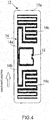
- the inlay 13 is, by referring to Figs. 3(b) and 4 , constituted by a base material 13a, an antenna 14, and an IC chip 15.
- the base material 13a is constituted by a synthetic resin film, and a linear antenna 14 made of a conductor is formed on the base material 13a and then, an IC chip 15 is bonded on this antenna 14 by using an electrically conductive adhesive, for example.
- the antenna 14 has an elongated shape with a conveyance direction as its longitudinal direction, and a loop-shaped antenna element 14a is provided at a center part in the longitudinal direction. And a dipole antenna element 14b connected to the loop-shaped antenna element 14a and extending linearly toward both front and rear ends in the longitudinal direction is provided.
- a meander line antenna element 14c connected to the dipole antenna element 14b and configured to be folded in a zigzag manner in a width direction orthogonal to the conveyance direction is provided in front and rear of the loop-shaped antenna element 14a in the longitudinal direction, respectively.
- the IC chip 15 incorporates a non-volatile memory such as EEPROM or the like in which memory is stored without power supply.
- the non-volatile memory of the IC chip 15 includes a tag ID storage region in which a unique number of each inlay 13 (hereinafter referred to as a tag ID) is stored in advance and a user storage region rewritable by a user.
- the IC chip 15 includes a communication function by an electromagnetic induction method for transmitting energy and signals by magnetic flux connection of an antenna coil of a reader/writer and the loop-shaped antenna element 14a of the antenna 14 and a radio wave method communication function for transmitting energy and signals by exchanging radio waves between the antenna of the reader/writer and the dipole antenna element 14b as well as the meander line antenna element 14c of the antenna 14.
- a placing base 2 has a placing plate 21 on which the IC tag continuous body 1 is placed.
- the placing plate 21 is constituted capable of changing a position of a placing surface with respect to the pre-processing device 3 and the post-processing device 5 and an angle of the placing surface in accordance with a size or a paper quality of the IC tag continuous body 1.
- the pre-processing device 3 is an encode device for writing data desired by a user such as a product number and the like in the respective IC tags 10 (the user storage region of the IC chip 15) of the IC tag continuous body 1.
- the pre-processing device 3 includes, by referring to Figs.
- the first tractor feeder unit 61 is arranged on an uppermost stream in reception of the IC tag continuous body 1 before issuance and by referring to Figs. 5 to 7 , an endless belt 61c extended between a driving roller 61a and a driven roller 61b and rotationally moved and a first tractor feeder driving motor 61d for rotationally moving the endless belt 61c through the driving roller 61a are provided, and on the endless belt 61c, feed pins 61e engaged with the sprocket holes 11 of the IC tag continuous body 1 are formed.
- the first tractor feeder unit 61 rotationally moves the endless belt 61c, the feed pins 61e are sequentially engaged with the sprocket holes 11, capable of being disengaged, so as to tract and convey the IC tag continuous body 1 toward the first conveyance unit 62 on a downstream side.
- the first rotary encoder unit 91 for detecting rotation of the driving roller 61a is provided on the driving roller 61a of the first tractor feeder unit 61.
- the first sensor 81 for detecting the detection mark 12 of the IC tag continuous body 1 is provided in the vicinity of the first tractor feeder unit 61.
- the first conveyance unit 62 is arranged at the downstream side of the first tractor feeder unit 61 and includes an endless conveyance belt 62c extended between a driving roller 62a and a driven roller 62b and rotationally moved and a first conveyance belt driving motor 62d for rotationally moving the conveyance belt 62c through the driving roller 62a.
- the first conveyance unit 62 conveys the IC tag continuous body 1 placed on an upper surface of the conveyance belt 62c toward the second conveyance unit 63 at the downstream side by rotationally moving the conveyance belt 62c.
- the second sensor 82 for detecting the detection mark 12 of the IC tag continuous body 1 is provided and is configured capable of detecting that the head of a page has reached between the first conveyance unit 62 and the second conveyance unit 63.
- a support plate 62e is arranged at positions in contact with a lower surface (inner peripheral surface) of the upper conveyance belt 62c. Therefore, when the IC tag continuous body 1 is conveyed from the upstream side toward the downstream side, the conveyance belt 62c is rotationally moved while sliding on the support plate 62e.
- suction holes 71b through which air is suctioned by rotation of a first suction fan 71a of the first negative pressure suction unit 71 and suction holes 72b through which air is suctioned by rotation of a second suction fan 72a of the second negative pressure suction unit 72 are formed in plural along the conveyance direction.
- a large number of through holes 62f are formed in the conveyance belt 62c. Therefore, by a negative pressure by the first negative pressure suction unit 71 and the second negative pressure suction unit 72, the IC tag continuous body 1 is conveyed in a state in close contact with the conveyance belt 62c.
- the second conveyance unit 63 is arranged at the downstream side of the first conveyance unit 62 and includes an endless conveyance belt 63c extended between a driving roller 63a and a driven roller 63b and rotationally moved and a second conveyance belt driving motor 63d for rotationally moving the conveyance belt 63c through the driving roller 63a.
- the second conveyance unit 63 conveys the IC tag continuous body 1 placed on the upper surface of the conveyance belt 63c toward the printing device 4 at the downstream side by rotationally moving the conveyance belt 63c.
- the third sensor 83 for detecting the detection mark 12 of the IC tag continuous body 1 is provided and is configured capable of detecting that the head of a page has reached between the second conveyance unit 63 and the printing device 4.
- a support plate 63e is arranged at a position in contact with a lower surface (inner peripheral surface) of the upper conveyance belt 63c. Therefore, when the IC tag continuous body 1 is conveyed from the upstream side toward the downstream side, the conveyance belt 63c is rotationally moved while sliding on the support plate 63e.
- suction holes 73b through which air is suctioned by rotation of a third suction fan 73a of the third negative pressure suction unit 73 and suction holes 74b through which air is suctioned by rotation of a fourth suction fan 74a of the fourth negative pressure suction unit 74 are formed in plural along the conveyance direction.
- a large number of through holes 63f are formed in the conveyance belt 63c. Therefore, by a negative pressure by the third negative pressure suction unit 73 and the fourth negative pressure suction unit 74, the IC tag continuous body 1 is conveyed in a state in close contact with the conveyance belt 63c.
- the first antenna unit 31 and the second antenna unit 32 are arranged close to and facing above the first conveyance unit 62.
- the first antenna unit 31 and the second antenna unit 32 are antennas conducting communication with the IC tag 10 by the electromagnetic induction method and have the same configuration.
- the first antenna unit 31 is used for reading the tag ID from the IC tag 10.
- the second antenna unit 32 is used for writing the desired data such as a product number and the like to the IC tag 10 (the user storage region of the IC chip 15).
- the data to be written to the IC tag 10 is called identification data.
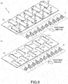
- configuration of the first antenna unit 31 will be described in detail by referring to Figs. 8 to 10 .
- row antenna units 31a to 31j are arranged at positions to face each row of the IC tags 10 from the first row to the tenth row of the IC tag continuous body 1 conveyed by the first conveyance unit 62, respectively.
- the row antenna units 31a to 31j are divided into the upstream-side row antenna units 31a to 31e and the downstream-side row antenna units 31f to 31j and arranged in a zigzag manner, in which the upstream-side row antenna units 31a to 31e are arranged at positions to face each row of the IC tags 10 on the odd-number rows, respectively, while the downstream-side row antenna units 31f to 31j are arranged at positions to face each row of the IC tags 10 on the even-number rows, respectively.
- a shield plate 310 is a support plate supporting the row antenna units 31a to 31j and is constituted by metal such as aluminum or a conductive substance such as a conductive resin.
- the shield plate 310 is arranged in parallel with and close to the IC tag continuous body 1 conveyed by the first conveyance unit 62, and opening portions 311a to 311j corresponding to the row antenna units 31a to 31j, respectively, are formed by being divided into the upstream opening portions 311a to 311e and the downstream opening portions 311f to 311j in a zigzag manner.
- Each of the opening portions 311a to 311j has an elongated and substantially rectangular shape with the conveyance direction as its longitudinal direction, in which, regarding the upstream-side opening portions 311a to 311e, the shape of only one corner on the upstream side is different, while regarding the downstream opening portions 311f to 311j, the shape of only one corner on the downstream side is different.
- regions formed between the upstream-side opening portions 311a to 311e and between the downstream opening portions 311f to 311j, respectively, are interfering preventing regions preventing interference among communication.
- the row antenna units 31a to 31j are constituted by a printed board 312 having a substantially same shape as those of the opening portions 311 a to 311j, a loop-shaped antenna element 313 formed on a lower surface of the printed board 312, an antenna terminal 314 installed upright on an upper surface opposite to the loop-shaped antenna element 313 on an end portion of the printed board 312, a ferrite sheet 315, and an antenna case 316 covering the printed board 312 from an upper surface side by referring to Figs. 9 and 10 .
- the shape of only one corner on the end portion side on which the antenna terminal 314 is installed upright is different.
- the antenna case 316 is constituted by metal such as aluminum or a conductive substance such as a conductive resin, an opening 316a for terminal through which the antenna terminal 314 is penetrated is formed, and by penetrating the antenna terminal 314 into the opening 316a for terminal in a state in which the ferrite sheet 315 is interposed between the antenna case 316 and the printed board 312 and by attaching a retaining ring, not shown, to the antenna terminal 314, the printed board 312 is fixed to the antenna case 316.
- the ferrite sheet 315 covers the loop-shaped antenna element 313 from the upper surface side of the printed board 312 and can suppress radiation from the printed board 312.
- the antenna case 316 is fixed to the upper surface side of the shield plate 310 by a screw 317 so that the printed boards 312 are fitted into the opening portions 311a to 311j.
- those other than the surface faced with the IC tag continuous body 1 are electromagnetically shielded, and the surface of the printed board 312 on which the loop-shaped antenna element 313 is formed is directly faced with the IC tag continuous body 1 conveyed by the first conveyance unit 62.
- the opening portions 311a to 311j and the printed board 312 only one corner has a different elongated and substantially rectangular shape and thus, they are fitted in one unique direction.
- the shape of only one corner at the upstream side is different and thus, in each of the row antenna units 31a to 31e at the upstream side, the antenna terminal 314 installed in contact on the end portion of the printed board 312 is located at the upstream side.
- each of the antenna terminals 314 of the row antenna units 31a to 31e arranged at the upstream side and each of the antenna terminals 314 of the row antenna units 31f to 31j arranged at the downstream side are respectively arranged in directions separated away from each other. As a result, interference between the each of the antenna terminals 314 of the row antenna units 31a to 31e arranged at the upstream side and each of the antenna terminals 314 of the row antenna units 31f to 31j arranged at the downstream side can be prevented.
- Reference numeral 318 denoted in Figs. 9 and 10 is a non-adhesive coating sheet such as a silicone coating sheet bonded to the lower surface of the shield plate 310 so as to cover the opening portions 311a to 311j. If the IC tag continuous body 1 is a label continuous body temporarily attached to a mount, by providing the non-adhesive coating sheet 318, adhesion of the label to the shield plate 310 can be prevented. The non-adhesive coating sheet 318 can be bonded so as to cover the whole shield plate 310 including the opening portions 311a to 311j on the lower surface.
- the third antenna unit 33 is arranged facing above the second conveyance unit 63.
- the third antenna unit 33 is an antenna conducting communication with the IC tag 10 by a radio wave method different from those of the first antenna unit 31 and the second antenna unit 32.
- the third antenna unit 33 is used for writing identification data to the IC tag 10.
- the printing device 4 is printing means for applying printing of data of a product or a producer or a barcode obtained by coding it or the like on the surfaces of the respective IC tags 10 of the IC tag continuous body 1.
- print data the data of a product or a producer or data such as a barcode obtained by coding it or the like to be printed on the surface of the IC tag 10 will be referred to as print data.
- the printing device 4 includes, by referring to Fig. 11 , a print unit 41, an optical fixation unit 42, and a filter unit 43 and by referring to Fig. 1 , a second tractor feeder unit 64, a third conveyance unit 65, a discharge roller 66, and a fifth negative pressure suction unit 75.
- the second tractor feed unit 64 is arranged at the uppermost stream receiving the IC tag continuous body 1 from the pre-processing device 3 and by referring to Fig. 11 , includes an endless belt 64c extended between a driving roller 64a and a driven roller 64b and rotationally moved and a second tractor feeder driving motor 64d for rotationally moving the endless belt 64c through the driving roller 64a, and on the endless belt 64c, feed pins 64e engaged with the sprocket holes 11 of the IC tag continuous body 1 are formed.
- the feed pins 64e are sequentially engaged with the sprocket holes 11, capable of being disengaged, so as to tract and convey the IC tag continuous body 1 toward the print unit 41 at a downstream side.
- a second rotary encoder unit 92 for detecting rotation of the driving roller 64a is provided on the driving roller 64a of the second tractor feeder unit 64.
- a fourth sensor 84 for detecting the detection mark 12 of the IC tag continuous body 1 is provided.
- the print unit 41 employs an electrophotography method such as a laser in which a latent image is formed by laser beams on a photosensitive drum, and this latent image is developed by a toner and then transferred to the surface of the IC tag 10.
- the print unit 41 applies printing of data of a product or a producer or a barcode obtained by coding it or the like on the surfaces of the respective IC tags 10 on the IC tag continuous body 1 and also prints a page number in a region in the vicinity of a page head other than the IC tag 10 or a region in which the sprocket holes 11 are formed, for example.
- a print method of the print unit 41 is not limited to the electrophotography method but a heat transfer method, a thermal method or an inkjet method can be also used.
- the third conveyance unit 65 is arranged at the downstream side of the print unit 41 and includes an endless conveyance belt 65c extended between a driving roller 65a and a driven roller 65b and rotationally moved and a third conveyance belt driving motor 65d for rotationally moving the conveyance belt 65c through the driving roller 65a.
- the third conveyance unit 65 conveys the IC tag continuous body 1 placed on the upper surface of the conveyance belt 65c toward the post-processing device 5 through the discharge roller 66 at the downstream side by rotationally moving the conveyance belt 65c.
- a support plate 65e is arranged at a position in contact with the lower surface (inner peripheral surface) of the upper conveyance belt 65c. Therefore, when the IC tag continuous body 1 is conveyed from the upstream side toward the downstream side, the conveyance belt 65c is rotationally moved while sliding on the support plate 65e.
- the optical fixation unit 42 fixes a toner image by melting toner having been transferred by the print unit 41 by irradiating flash light using a xenon tube or the like to the surface of the IC tag continuous body 1 conveyed by the third conveyance unit 65.
- the toner image can be fixed in a non-contact manner without causing damage (external force) to the IC tag 10.
- the filter unit 43 is an air filter for erasing gas or odor generated in optical fixation by the optical fixation unit 42.
- the post-processing device 5 verifies that the identification data has been correctly written in the respective IC tags 10 of the IC tag continuous body 1 and also marks the IC tag 10 in which the identification data has not been correctly written.
- the post-processing device 5 includes, by referring to Fig. 12 , a fourth antenna unit 51, an emboss processing unit 52, a fourth conveyance unit 67, a sixth negative pressure suction unit 76, a seventh negative pressure suction unit 77, a page-number reading unit 93, a fifth sensor 85, a sixth sensor 86, and a seventh sensor 87.
- the fourth conveyance unit 67 includes an endless conveyance belt 67c arranged at the uppermost stream of the post-processing device 5 receiving the IC tag continuous body 1 from the printing device 4 and extended between a driving roller 67a and a driven roller 67b and rotationally moved, and a fourth conveyance belt driving motor 67d for rotationally moving the conveyance belt 67c through the driving roller 67a.
- the fourth conveyance unit 67 conveys the IC tag continuous body 1 placed on the upper surface of the conveyance belt 67c toward the emboss processing unit 52 at the downstream side by rotationally moving the conveyance belt 67c.
- the sixth sensor 86 for detecting the detection mark 12 of the IC tag continuous body 1 is provided and is configured capable of detecting that the head of a page has reached between the fourth conveyance unit 67 and the emboss processing unit 52.
- the seventh sensor 87 for detecting the detection mark 12 of the IC tag continuous body 1 is provided and is configured capable of detecting jamming or the like at the emboss processing unit 52.
- a support plate 67e is arranged at a position in contact with a lower surface (inner peripheral surface) of the upper conveyance belt 67c. Therefore, when the IC tag continuous body 1 is to be conveyed from the upstream side toward the downstream side, the conveyance belt 67c is rotationally moved while sliding on the support plate 67e.
- suction holes through which air is suctioned by rotation of the sixth suction fan 76a of the sixth negative pressure suction unit 76 and suction holes through which the air is suctioned by rotation of the seventh suction fan 77a of the seventh negative pressure suction unit 77 are formed in plural along the conveyance direction.
- the conveyance belt 67c a large number of though holes are formed. Therefore, the IC tag continuous body 1 is conveyed by the negative pressures by the sixth negative pressure suction unit 76 and the seventh negative pressure suction unit 77 in a state in close contact with the conveyance belt 67c.
- the fifth sensor 85 is arranged at the vicinity of the uppermost stream in the post-processing device 5 receiving the IC tag continuous body 1 from the printing device 4 and is configured capable of detecting that the head of the page has reached the post-processing device 5.
- the page-number reading unit 93 is also arranged at the vicinity of the uppermost stream receiving the IC tag continuous body 1 from the printing device 4, and when the fact that the head of the page has reached the post-processing device 5 is detected by the fifth sensor 85, by photographing the surface of the IC tag continuous body 1, the page number printed by the printing device 4 is read.
- the fourth antenna unit 51 is arranged facing above the fourth conveyance unit 67.
- the fourth antenna unit 51 is an antenna conducting communication with the IC tag 10 by a radio wave method different from those of the first antenna unit 31 and the second antenna unit 32.
- the fourth antenna unit 51 is used for reading the tag ID and the identification data written to the IC tag 10 from the IC tag 10 conveyed by the fourth conveyance unit 67.
- the emboss processing unit 52 includes, by referring to Fig. 12 , cutter members 53 corresponding to each row of the IC tags 10 arranged in multiple rows, respectively, are formed.
- the cutter member 53 is mark giving means for executing emboss processing of cutting and bending a part of an end portion of the IC tag 10. Then, the emboss processing unit 52 executes the emboss processing by cutting/raising and bending the part of the end portion by using the cutter member 53 to the IC tag 10 in which the identification data could not be correctly written.
- the first antenna unit 31 as well as the second antenna unit 32, the third antenna unit 33, and the fourth antenna unit 51 are arranged facing the conveyance belt 62c of the first conveyance unit 62 as well as the support plate 62e, the conveyance belt 63c of the second conveyance unit 63 as well as the support plate 63e, and the conveyance belt 67c of the fourth conveyance unit 67 as well as the support plate 67e, respectively.
- the conveyance belts 62c, 63c, and 67c as well as the support plates 62e, 63e, and 67e preferably have low dielectric constants so that a resonant frequency of the antenna of the IC tag continuous body 1 (IC tags 10) does not change in order to keep transaction between the IC tag continuous body 1 (IC tags 10) facing each of the antenna units favorable.
- the conveyance belts 62c, 63c, and 67c slide in a state subjected to a negative pressure in directions of the support plates 62e, 63e, and 67e, respectively, and thus, it is important that friction caused by sliding between the conveyance belts 62c, 63c, and 67c and the support plates 62e, 63e, and 67e is small, and the conveyance belts 62c, 63c, and 67c and the support plates 62e, 63e, and 67e have excellent friction resistance (material with low friction coefficients) and hard to be electrically charged.
- urethane belts are used for the conveyance belts 62c, 63c, and 67c
- POM (polyacetal resin) plates are used for the support plates 62e, 63e, and 67e.
- the IC tag issuing apparatus of this embodiment includes, by referring to Fig. 13 , a conveyance control unit 101, a writing control unit 102, a print control unit 103, an information storage unit 110, a tag ID reading unit 121, a first identification data writing unit 122, a second identification data writing unit 123, and an identification data reading unit 124.
- the conveyance control unit 101 is an information processing unit such as a microcomputer including a CPU (Central Processing Unit), a ROM (Read Only Memory), RAM (Random Access Memory) and the like.
- the ROM of the conveyance control unit 101 stores a control program for performing conveyance control of the IC tag continuous body 1.
- the conveyance control unit 101 causes the IC tag continuous body 1 to be conveyed by controlling a conveyance constituent element group (the first tractor feeder driving motor 61d, the first conveyance belt driving motor 62d, the second conveyance belt driving motor 63d, the second tractor feeder driving motor 64d, the third conveyance belt driving motor 65d, the fourth conveyance belt driving motor 67d) and a suction constituent element group (the first suction fan 71a, the second suction fan 72a, the third suction fan 73a, the fourth suction fan 74a, the firth suction fan 75a, the sixth suction fan 76a, the seventh suction fan 77a) in accordance with inputs from a position sensor group (the first sensor 81, the first rotary encoder unit 91, the second sensor 82, the third sensor 83, the fourth sensor 84, the second rotary encoder unit 92, the fifth sensor 85, the sixth sensor 86, the seventh sensor 87) by reading the control program stored in the ROM and extending the control program to
- the writing control unit 102 is an information processing unit such as a microcomputer or the like including a CPU (Central Processing Unit), a ROM (Read Only Memory), RAM (Random Access Memory) and the like.
- the ROM of the writing control unit 102 stores a control program for writing the identification data in the respective IC tags 10 of the IC tag continuous body 1.
- the writing control unit 102 writes the identification data in the respective IC tags 10 of the IC tag continuous body 1 by reading the control program stored in the ROM and by extending the control program to the RAM so as to control a communication constituent element group (the tag ID reading unit 121, the first identification data writing unit 122, the second identification data writing unit 123, the identification data reading unit 124).
- the print control unit 103 is an information processing unit such as a microcomputer including a CPU (Central Processing Unit), a ROM (Read Only Memory), RAM (Random Access Memory) and the like.
- the ROM of the print control unit 103 stores a control program for operating the print unit 41 and the optical fixation unit 42.
- the print control unit 103 causes the print data to be printed on the surfaces of the respective IC tags 10 of the IC tag continuous body 1 by reading the control program stored in the ROM and by extending the control program to the RAM so as to control the print unit 41 and the optical fixation unit 42.
- the information storage unit 110 is storage means such as a semiconductor memory, a HDD (Hard Disk Drive) and the like and includes a product information storage portion 111, a page information storage portion 112, and a reissuance information storage portion 113.
- the product information storage portion 111 is storage means for storing product information input through a network, not shown, or various recording media.
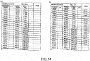
- the product information is list information composed of identification data (management number and the like) to be written to the respective IC tags 10 of the IC tag continuous body 1, print data (product number, product name and the like) to be printed on the surfaces of the respective IC tags 10 of the IC tag continuous body 1, and the tag ID of the IC tag 10 in which the identification data is written as illustrated in Fig. 14 .
- the tag ID is empty as illustrated in Fig. 14(a) until the identification data is written to the IC tag 10, and the tag ID of the IC tag 10 in which the identification data has been written is described as illustrated in Fig. 14(b) after the identification data is written to the IC tag 10.
- the page information storage portion 112 is storage means for storing page information generated for each page of the IC tag continuous body 1.
- the page information is composed of, by referring to Fig. 15(a) , matrix information indicating a position of the tag ID on the page, the read-out tag ID, the identification data (management number and the like) to be written in the respective IC tags 10 of one page, the print data (product number, product name and the like) to be printed on the surfaces of the respective IC tags 10 of one page, and the tag ID of the IC tag 10 in which the identification data is written.
- a storage region may be ensured on the RAM of the writing control unit 102 or the print control unit 103 so as to be used as a buffer.
- the reissuance information storage portion 113 is storage means for storing reissuance information for reissuance altogether at the end.
- the reissuance information is composed of, by referring to Fig. 15(b) , the identification data which failed to be written to the IC tag 10 and the corresponding print data (product number, product name and the like).
- a flag indicating whether or not writing to the IC tag 10 has succeeded may be provided in the product information stored in the product information storage portion 111 so that the product information is used as the reissuance information.
- the tag ID reading unit 121 is a reader/writer for reading the tag ID from the IC tag 10 of the IC tag continuous body 1 being conveyed by the first conveyance unit 62 by an electromagnetic induction method by using the first antenna unit 31.
- the tag ID reading unit 121 has a function of conducting communication with the IC tag 10 through a plurality of channels with different frequencies and is configured to use different channels for the row antenna units 31a to 31j adjacent at least in the width direction and a diagonal direction.
- the first identification data writing unit 122 is a reader/writer for writing the identification data by the electromagnetic induction method to the IC tag 10 of the IC tag continuous body 1 being conveyed by the first conveyance unit 62 by using the second antenna unit 32.
- the first identification data writing unit 122 has a function of conducting communication with the IC tag 10 through a plurality of channels with different frequencies and is configured to use different channels for the row antenna units 32a to 32j adjacent at least in the width direction and the diagonal direction.
- the second identification data writing unit 123 is a reader/writer for writing the identification data by the radio wave method to the IC tag 10 of the IC tag continuous body 1 being conveyed by the second conveyance unit 63 by using the third antenna unit 33.
- the identification data reading unit 124 is a reader/writer for reading the tag ID and the identification data by the radio wave method from the IC tag 10 of the IC tag continuous body 1 being conveyed by the fourth conveyance unit 67 by using the fourth antenna unit 51.
- the conveyance control unit 101 causes the IC tag continuous body 1 to be conveyed by controlling the conveyance constituent element group (the first tractor feeder driving motor 61d, the first conveyance belt driving motor 62d, the second conveyance belt driving motor 63d, the second tractor feeder driving motor 64d, the third conveyance belt driving motor 65d, the fourth conveyance belt driving motor 67d).
- the conveyance constituent element group the first tractor feeder driving motor 61d, the first conveyance belt driving motor 62d, the second conveyance belt driving motor 63d, the second tractor feeder driving motor 64d, the third conveyance belt driving motor 65d, the fourth conveyance belt driving motor 67d.
- conveyance of the IC tag continuous body 1 is performed on the basis of a print speed of the printing device 4, and a series of processing is executed in the pre-processing device 3 and the post-processing device 5 in a state in which the IC tag continuous body 1 is being conveyed at all times.
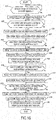
- the conveyance control unit 101 waits for detection of the detection mark 12 by the first sensor 81 provided in the vicinity of the first tractor feeder unit 61 (Step A01). Then, when the detection mark 12 notifying start of a page is detected by the first sensor 81, the detection of the detection mark 12 is notified to the writing control unit 102.
- the writing control unit 102 notified of the detection of the detection mark 12 generates blank page information (Step A02).
- the conveyance control unit 101 grasps a conveyance distance of the IC tag continuous body 1 by a detection result of the first rotary encoder unit 91 and waits for arrival of the IC tags 10 on the first line at the row antenna units 31a to 31e located at the upstream side in the first antenna unit 31 (Step A03). Specifically, when all the loop-shaped antenna elements 14a of the IC tags 10 on the odd-number rows on the first line enter the loop-shaped antenna elements 313 of the row antenna units 31a to 31e, it is determined to be arrival.
- the writing control unit 102 causes the tag IDs from the IC tags 10 on the odd-number rows on the first line to be read by the tag ID reading unit 121, respectively (Step A04) and describes the read tag IDs in the page information generated at Step A02 (Step A05).
- a data record of the IC tag 10 from which the tag ID could not be read is maintained in a blank state.
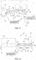
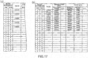
- Fig. 17(a) illustrates a state in which the tag IDs are successfully read from all the IC tags 10 on the odd-number rows on the first line, respectively, and the read tag IDs are described in the page information.
- the conveyance control unit 101 grasps the conveyance distance of the IC tag continuous body 1 by the detection result of the first rotary encoder unit 91 and waits for the arrival of the IC tags 10 on the first line at the row antenna units 31f to 31j located at the downstream side in the first antenna unit 31 (Step A06). Specifically, when all the loop-shaped antenna elements 14a of the IC tags 10 on the even-number rows on the first line enter the loop-shaped antenna elements 313 of the row antenna units 31f to 31j, it is determined to be arrival.
- the writing control unit 102 causes the tag IDs to be read by the tag ID reading unit 121 from the IC tags 10 on the even-number rows on the first line, respectively (Step A07) and describes the read tag IDs in the page information generated at Step A02 (Step A08).
- the normal IC tags 10 on the first line are determined on the basis of the fact whether the tag ID is described or not.
- the writing control unit 102 sequentially reads the identification data and the print data to be stored in the normal IC tags 10 on the first line from the product information and describes the read identification data and print data in the data record of the page information in which the tag IDs are described (Step A09).
- Fig. 17(b) illustrates a state in which the tag IDs are successfully read also from all the IC tags 10 on the even-number rows on the first line, respectively, the tag IDs are described in all the data records on the first line in the page information, respectively, and moreover, the identification data and the print data read out of the product information are described.
- the identification data and the print data read out of the product information and described in the page information are controlled by a flag or the like so that they are not read out from the product information and described in the page information again.
- the conveyance control unit 101 grasps the conveyance distance of the IC tag continuous body 1 by the detection result of the first rotary encoder unit 91 and waits for the arrival of the IC tags 10 on the second line at the row antenna units 31a to 31e located at the upstream side in the first antenna unit 31 (Step A10). Specifically, when all the loop-shaped antenna elements 14a of the IC tags 10 on the odd-number rows on the second line enter the loop-shaped antenna elements 313 of the row antenna units 31a to 31e, it is determined to be arrival.
- the writing control unit 102 causes the tag IDs to be read by the tag ID reading unit 121 from the IC tags 10 on the odd-number rows on the second line, respectively (Step A11) and describes the read tag IDs in the page information generated at Step A02 (Step A12).
- the conveyance control unit 101 grasps the conveyance distance of the IC tag continuous body 1 by the detection result of the first rotary encoder unit 91 and waits for the arrival of the IC tags 10 on the second line at the row antenna units 31f to 31j located at the downstream side in the first antenna unit 31 (Step A13). Specifically, when all the loop-shaped antenna elements 14a of the IC tags 10 on the even-number rows on the second line enter the loop-shaped antenna elements 313 of the row antenna units 31f to 31j, it is determined to be arrival.
- the writing control unit 102 causes the tag IDs to be read by the tag ID reading unit 121 from the IC tags 10 on the even-number rows on the second line, respectively (Step A14) and describes the read tag IDs in the page information generated at Step A02 (Step A15).
- the normal IC tags 10 on the second line are determined on the basis of the fact whether the tag ID is described or not.
- the writing control unit 102 sequentially reads the identification data and the print data to be stored in the normal IC tags 10 on the second line from the product information and describes the read identification data and print data in the data record of the page information in which the tag IDs are described (Step A16).
- Fig. 15(a) illustrates a state in which the tag IDs could not be read out of the IC tags 10 on the first row on the second line and the data record on the first row on the second line is blank.
- the reading of the tag IDs at Steps A04, A07, A11, and A14 may be performed several times until the IC tag 10 goes out of the communication region of the row antenna units 31a to 31j (until the loop-shaped antenna elements 14a of the IC tags 10 go out of the loop-shaped antenna elements 313 of the row antenna units 31a to 31j).
- the tag-ID reading operation at Steps A1 to A16 is performed in order to determine whether or not the IC tag 10 functions normally. Therefore, whether or not the IC tag 10 is normal is determined on the basis of whether or not the tag ID is described in the page information.
- timing when the IC tags 10 on the first line reach the row antenna units 31f to 31j located at the downstream side in the first antenna unit 31 at Step A06 and timing when the IC tags 10 on the second line reach the row antenna units 31a to 31e located on the upstream side in the first antenna unit 31 at Step A10 can be switched or substantially the same depending on a pitch of the IC tags 10 or a size or layout of the row antenna units 31a to 31j.
- the communication is conducted at the same time in the row antenna units 31a to 31e located at the upstream side and the row antenna units 31f to 31j located at the downstream side, but since the row antenna units 31a to 31j adjacent in the diagonal direction conduct communication by using different channels, interference can be prevented and communication can be reliably conducted with the targeted IC tags 10.
- the conveyance control unit 101 grasps the conveyance distance of the IC tag continuous body 1 by the detection result of the first rotary encoder unit 91 and waits for the arrival of the IC tags 10 on the first line at the row antenna units 32a to 32e located at the upstream side in the second antenna unit 32 (Step B01). Specifically, when all the loop-shaped antenna elements 14a of the IC tags 10 on the odd-number rows on the first line enter the loop-shaped antenna elements 313 of the row antenna units 32a to 32e, it is determined to be arrival.
- the writing control unit 102 causes the identification data described in the page information to be written by the first identification data writing unit 122 to the IC tags 10 on the odd-number rows on the first line (Step B02) and determines whether or not the writing has succeeded in all (Step B03).
- the writing control unit 102 extracts the data record including the identification data which failed to be written (tag ID and identification data) from the page information (Step B04) and temporarily stores it in the RAM or the like.
- the conveyance control unit 101 grasps the conveyance distance of the IC tag continuous body 1 by the detection result of the first rotary encoder unit 91 and waits for the arrival of the IC tags 10 on the first line at the row antenna units 32f to 32j located at the downstream side in the second antenna unit 32 (Step B05). Specifically, when all the loop-shaped antenna elements 14a of the IC tags 10 on the even-number rows on the first line enter the loop-shaped antenna elements 313 of the row antenna units 32f to 32j, it is determined to be arrival.
- the writing control unit 102 causes the identification data described in the page information to be written by the first identification data writing unit 122 to the IC tags 10 on the even-number rows on the first line (Step B06) and determines whether or not the writing has succeeded in all (Step B07).
- the writing control unit 102 extracts the data record including the identification data which failed to be written (tag ID and identification data) from the page information (Step B08) and temporarily stores it in the RAM or the like.
- the conveyance control unit 101 grasps the conveyance distance of the IC tag continuous body 1 by the detection result of the first rotary encoder unit 91 and waits for the arrival of the IC tags 10 on the second line at the row antenna units 32a to 32e located at the upstream side in the second antenna unit 32 (Step B09). Specifically, when all the loop-shaped antenna elements 14a of the IC tags 10 on the odd-number rows on the second line enter the loop-shaped antenna elements 313 of the row antenna units 32a to 32e, it is determined to be arrival.
- the writing control unit 102 causes the identification data described in the page information to be written by the first identification data writing unit 122 to the IC tags 10 on the odd-number rows on the second line (Step B10) and determines whether or not the writing has succeeded in all (Step B11).
- the writing control unit 102 extracts the data record including the identification data which failed to be written (tag ID and identification data) from the page information (Step B12) and temporarily stores it in the RAM or the like.
- the conveyance control unit 101 grasps the conveyance distance of the IC tag continuous body 1 by the detection result of the first rotary encoder unit 91 and waits for the arrival of the IC tags 10 on the second line at the row antenna units 32f to 32j located at the downstream side in the second antenna unit 32 (Step B13). Specifically, when all the loop-shaped antenna elements 14a of the IC tags 10 on the even-number rows on the second line enter the loop-shaped antenna elements 313 of the row antenna units 32f to 32j, it is determined to be arrival.
- the writing control unit 102 causes the identification data described in the page information to be written by the first identification data writing unit 122 to the IC tags 10 on the even-number rows on the second line (Step B14) and determines whether or not the writing has succeeded in all (Step B015).
- the writing control unit 102 extracts the data record including the identification data which failed to be written (tag ID and identifcation data) from the page information (Step B12) and temporarily stores it in the RAM or the like.
- the writing of the identification data at Steps B02, B06, B10, and B13 may be performed several times until the IC tag 10 goes out of the communication region of the row antenna units 32a to 32j (until the loop-shaped antenna elements 14a of the IC tags 10 go out of the loop-shaped antenna elements 313 of the row antenna units 32a to 32j).
- the writing of the identification data at Steps B02, B06, B10, and B14 is performed to the IC tags 10 from which the tag IDs can be read and whose identification data is described in the page information. Moreover, the writing of the identification data at Steps B02, B06, B10, and B14 is performed directly without checking the tag IDs of the IC tags 10 since the target IC tag 10 is specified.
- the timing when the IC tags 10 on the first line reach the row antenna units 32f to 32j located at the downstream side in the second antenna unit 32 at Step B05 and the timing when the IC tags 10 on the second line reach the row antenna units 32a to 32e located at the upstream side in the second antenna unit 32 at Step B09 can be switched or substantially the same depending on a pitch of the IC tags 10 or a size or a layout of the row antenna units 32a to 32j.
- the communication is conducted at the same time in the row antenna units 32a to 32e located at the upstream side and the row antenna units 32f to 32j located at the downstream side, but since the row antenna units 32a to 32j adjacent in the diagonal direction conduct communication by using different channels, interference can be prevented and communication can be reliably conducted with the targeted IC tags 10.
- the conveyance control unit 101 grasps the conveyance distance of the IC tag continuous body 1 by the detection result of the first rotary encoder unit 91 and waits for the arrival of the IC tags 10 in which the identification data is written at Steps B02, B06, B10, and B13 at the communication region of the third antenna unit 32 (Step B17). Then, when the IC tags 10 in which the identification data is written at Steps B02, B06, B10, and B13 reach the communication region of the third antenna unit 33, the fact is notified from the conveyance control unit 101 to the writing control unit 102.
- the writing control unit 102 causes the identification data to be written by the second identification data writing unit 123 to the IC tags 10 which failed writing of the identification data at Steps B02, B06, B10, and B13 (Step B18).
- the second identification data writing unit 123 writes the identification data to the IC tag 10 by specifying the tag ID on the basis of the data record extracted at Steps B04, B08, B12, and B16.
- the second identification data writing unit 123 conducts communication with the IC tag 10 in the electric wave method by using the third antenna unit 33, its communication region is wider than that of the electromagnetic induction method, but since the first antenna unit 31 and the second antenna unit 32 are electromagnetically shielded except the surface faced with the IC tag continuous body 1, interference with the communication by the tag ID reading unit 121 or the first identification data writing unit 122 is prevented.
- the conveyance control unit 101 grasps the conveyance distance of the IC tag continuous body 1 by the detection result of the first rotary encoder unit 91 and notifies the printing device 4 of the arrival of the page. Then, the printing device 4 detects a head of the page by detecting the detection mark 12 by the fourth sensor 84, prints a page number on the page, and prints the print data described in the page information on the surface of the IC tag 10 of the page, respectively (Step B19).
- the conveyance control unit 101 notifies the detection of the detection mark 12 to the page-number reading unit 93 and the writing control unit 102 and causes the page-number reading unit 93 to read the page number printed on the page (Step B20).
- the reading of the page number is performed in order to specify the page. Therefore, a sign such as a barcode may be printed other than the page number so as to be read, but by printing the page number with which the user can directly recognize the page, manual inspection can be facilitated.
- the writing control unit 102 causes the identification data reading unit 124 to read the tag ID and the identification data from the IC tag 10 of the IC tag continuous body 1 being conveyed by the fourth conveyance unit 67 by using the fourth antenna unit 51 (Step B21). Then, the writing control unit 102 compares the tag ID and the identification data read at Step B21 with the page information of the page number read by the page-number reading unit 93 (Step B22) and determines whether or not all the data records are matched (Step B23).
- Step B23 If there is an unmatched data record at Step B23, that is, if the identification data described in the page information could not be read or if the identification data is written to the IC tag 10 with the tag ID different from the page information, the identification data and the print data as the unmatched data record are described as reissuance information in the reissuance information storage portion 113 (Step B24).
- Fig. 15(b) illustrates an example in which the identification data described in the page information could not be read from the IC tag 10 on the fifth row on the first line and the identification data and the print data of the fifth row on the first line are described as the reissuance information.
- Step B25 the tag ID of the data record determined to be matched at Step B23 is described in the product information (Step B25), and the issuing operation for one page is finished.
- the issuing operation at Step A01 to Step B25 is subjected to parallel processing for each page. Then, after the issuing operation on the basis of the product information is finished, the issuing operation on the basis of the reissuance information is performed.
- the writing control unit 102 notifies position information of the IC tag 10 from which the tag ID could not be read and the IC tag 10 whose identification data did not match the page information to the emboss processing unit 52. Then, the emboss processing unit 52 applies the emboss processing to and issues the IC tag 10 from which the tag ID could not be read and the IC tag 10 whose identification data did not match the page information.
- the IC tag 10 in which the identification data could not be correctly written can be selected easily and can be replaced by the IC tag 10 issued on the basis of the reissuance information.
- 10 rows * 2 lines of the IC tags 10 constitute one page, but the number of rows and the number of lines constituting one page are arbitrary.
- the numbers and layout of the row antenna units 31a to 31j in the first antenna unit 31 and the row antenna units 32 a to 32j in the second antenna unit 32 are set as appropriate.
- the IC tag issuing apparatus for writing the identification data to the IC tags 10 arranged in multiple rows aligned as the IC tag continuous body 1, respectively, and issuing the result includes the second antenna units 32 arranged to face each row of the IC tags 10 in multiple rows, respectively, and functioning as a plurality of writing row antenna units for writing the identification data to the IC tags 10 by the electromagnetic induction method and a third antenna unit 33 arranged at the downstream side in the conveyance direction of the IC tag continuous body 1 from the second antenna unit 32 and functioning as the electric-wave antenna unit for writing the identification data to the IC tags 10 by the electric wave method and is constituted to write the identifcation data by using the third antenna units 33 to the IC tag 10 in which the identification data could not be written by using the second antenna unit 32.
- the identification data can be written by the third antenna unit 33 and thus, the communication processing with the IC tag can be conducted at a high speed and reliably, whereby the issuance speed can be improved.
- the first antenna unit 31 arranged to face each row of the IC tags 10 arranged in multiple rows, respectively, and functioning as a plurality of reading row antenna units for reading the unique tag ID from the IC tag 10 by the electromagnetic induction method is provided and it is constituted so that the identification data is written by using the second antenna unit 32 to the IC tag 10 from which the tag ID could be read by using the first antenna unit 31.
- the writing of the identification data using the third antenna unit 33 is performed by specifying the tag ID.
- the IC tag 10 in which the identification data could not be written by using the second antenna unit 32 can be specified in a pinpoint manner.
- the surfaces other than the surface faced with the IC tag 10 of the IC tag continuous body 1 is electromagnetically shielded.
- the first conveyance unit 62 and the second conveyance unit 63 are provided as the conveyance unit for conveying the IC tag continuous body 1 while suctioning it to the conveyance belts (62c, 63c), and the second antenna unit 32 is arranged to face the IC tags 10 of the IC tag continuous body 1 conveyed by the first conveyance unit 62, and the third antenna unit 33 is arranged to face the IC tags 10 of the IC tag continuous body 1 conveyed by the second conveyance unit 63.
- the IC tags 10 of the IC tag continuous body 1 can conduct communication in a state reliably faced with the second antenna unit 32 and the third antenna unit 33, whereby communication accuracy can be improved.
Landscapes
- Engineering & Computer Science (AREA)
- Physics & Mathematics (AREA)
- General Physics & Mathematics (AREA)
- Theoretical Computer Science (AREA)
- Microelectronics & Electronic Packaging (AREA)
- Health & Medical Sciences (AREA)
- Toxicology (AREA)
- Electromagnetism (AREA)
- Artificial Intelligence (AREA)
- Computer Vision & Pattern Recognition (AREA)
- General Health & Medical Sciences (AREA)
- Computer Networks & Wireless Communication (AREA)
- Computer Hardware Design (AREA)
- Credit Cards Or The Like (AREA)
- Conveying Record Carriers (AREA)
Abstract
Description
- The present invention relates to an IC tag issuing apparatus writing desired identification data to each of IC tags of an IC tag continuous body on which the IC tags are aligned in multiple rows in a non-contact manner and issuing it.
- In recent years, technologies for facilitating inventory control, sales control and the like of merchandises by an RFID (radio frequency identification) using an IC tag having an IC chip and an antenna and making electric writing/reading of information in a non-contact manner possible is proposed. The IC chip and the antenna are contained in a sheet such as a label, a price tag and the like as an inlay (inlet) formed on a film in general, and an IC tag is configured. The inlay itself including the IC chip and the antenna is also called an IC tag, an electronic tag, a wireless tag and an RFID tag in some cases but in this Description, a sheet such as a merchandise tag (price tag), a label and the like including the IC chip and the antenna is called an IC tag.
- The IC tag is offered as an IC tag continuous body on which the IC tags are continuously aligned in general in many cases, and an IC tag issuing apparatus which writes desired data such as a product number to the IC tag continuous body in a non-contact manner and applies printing of data of the product or a producer or a barcode obtained by coding it or the like on a surface of each of them and issues the result is proposed (see
Patent Literature 1, for example). - Patent Literature 1:
Japanese Patent Laid-Open No. 2006-338179 - In recent years, usage of the IC tags has increased, and needs for a large quantity of issuance of the IC tags at a high speed has heightened. In order to improve an issuance speed of the IC tag, a conveyance speed of an IC tag continuous body needs to be increased, but a speed of communication with the IC tag has limitation, and if the issuance speed is improved by increasing the conveyance speed of the IC tag continuous body, defective writing to the IC tag occurs, and yield is worsened, which is a problem.
- An object of the present invention is to solve the problem of the prior-art technology in view of the problem and to provide an IC tag issuing apparatus capable of executing communication processing with the IC tag at a high speed and reliably and of improving the issuance speed.
- The present invention solves the problem by means for solving below.
- An IC tag issuing apparatus of the present invention is an IC tag issuing apparatus for writing identification data to IC tags, the IC tags arranged in multiple rows aligned as an IC tag continuous body, and issuing the result, the IC tag issuing apparatus including a plurality of writing row antenna units arranged to face each row of the IC tags arranged in multiple rows, respectively, for writing the identification data to the IC tags by an electromagnetic induction method and an electric-wave antenna unit arranged at a downstream side in a conveyance direction of the IC tag continuous body from the plurality of writing row antenna units for writing the identification data to the IC tags by an electric wave method, characterized in that the identification data is written by using the electric-wave antenna unit to the IC tags to which the identification data could not be written by using the plurality of writing row antenna units.
- Moreover, in the IC tag issuing apparatus of the present invention, further including at an upstream side in the conveyance direction of the IC tag continuous body from the plurality of writing row antenna units, a plurality of reading row antenna units arranged to face each row of the IC tags arranged in multiple rows, respectively, and read a unique tag ID from the IC tag by the electromagnetic induction method may be provided, and the identification data may be written by using the plurality of writing row antenna units to the IC tags from which the tag ID could be read by using the plurality of reading row antenna units.
- Moreover, in the IC tag issuing apparatus of the present invention, the writing of the identification data using the electric-wave antenna unit may be conducted by specifying the tag ID.
- Moreover, in the IC tag issuing apparatus of the present invention, in the writing row antenna unit, surfaces other than the surface faced with the IC tag of the IC tag continuous body may be electromagnetically shielded.
- Moreover, in the IC tag issuing apparatus of the present invention, a conveyance unit for conveying the IC tag continuous body while suctioning it to a conveyance belt may be provided, and the writing row antenna unit and the electric-wave antenna unit may be arranged to face each row of the IC tags of the IC tag continuous body conveyed by the conveyance unit. Advantageous Effect of the Invention
- According to the present invention, such an effect that the communication processing with the IC tag can be executed at a high speed, and the issuance speed can be improved is exerted.
-
-
Fig. 1 is a schematic side view illustrating configuration of an embodiment of an IC tag issuing apparatus according to the present invention. -
Fig. 2 is a top view illustrating configuration of a part of an IC tag continuous body illustrated inFig. 1 . -
Fig. 3 is an enlarged front view and a sectional view illustrating configuration of an IC tag illustrated inFig. 2 . -
Fig. 4 is a front view illustrating configuration of inlay illustrated inFig. 3 . -
Fig. 5 is a schematic side view illustrating configuration of a pre-processing device illustrated inFig. 1 . -
Fig. 6 is a schematic top view illustrating the configuration of the pre-processing device illustrated inFig. 1 . -
Fig. 7 is a schematic top view illustrating configuration of a support plate in the pre-processing device illustrated inFig. 1 . -
Fig. 8 is a perspective view illustrating configuration of a first antenna unit illustrated inFig. 5 . -
Fig. 9 is an exploded perspective view illustrating configuration of a row antenna unit illustrated inFig. 8 . -
Fig. 10 is a sectional view illustrating the configuration of the row antenna unit illustrated inFig. 8 . -
Fig. 11 is a schematic side view illustrating configuration of a printing device illustrated inFig. 1 . -
Fig. 12 is a schematic side view illustrating configuration of a post-processing device illustrated inFig. 1 . -
Fig. 13 is a block diagram illustrating configuration of a control unit controlling an operation of an embodiment of an IC tag issuing apparatus according to the present invention. -
Fig. 14 is a view illustrating a product information example stored in an information storage unit illustrated inFig. 13 . -
Fig. 15 is a view illustrating a page information example and a reissuance information example stored in an information storage unit illustrated inFig. 13 . -
Fig. 16 is a flowchart for explaining a tag ID reading operation in an embodiment of the IC tag issuing apparatus according to the present invention. -
Fig. 17 is an explanatory view for explaining the tag ID reading operation of the embodiment of the IC tag issuing apparatus according to the present invention. -
Fig. 18 is a flowchart for explaining an identification data writing operation of the embodiment of the IC tag issuing apparatus according to the present invention. - An IC tag issuing apparatus of this embodiment writes desired data in each of IC chips of an IC tag
continuous body 1 in a non-contact manner and also applies printing of information of a product or a producer, a barcode obtained by coding it or the like on the respective surfaces and issues the result. The IC tag issuing apparatus includes a placingbase 2 on which the IC tagcontinuous body 1 before issuance is placed, apre-processing device 3, aprinting device 4, apost-processing device 5, and the placingbase 2 on which the issued IC tagcontinuous body 1 is placed by referring toFig. 1 . - The IC tag
continuous body 1 is a continuous sheet (fan-folded sheet) in which a page on whichIC tags 10 are aligned in multiple rows is folded alternately by referring toFig. 2 . In this embodiment, 20 pieces, that is, 10 pieces * 2 lines of theIC tags 10 from a first row to a tenth row are arranged on one page. On both sides of the IC tagcontinuous body 1, sprocketholes 11 are formed at an equal interval. Moreover, in the vicinity of a head of a conveyance direction in a region in which thesprocket holes 11 are formed, adetection mark 12 indicating start of the page is printed. The IC tagcontinuous body 1 may be a rolled sheet wound in a roll state and in this case, thedetection mark 12 indicating the start of theIC tag 10 only needs to be printed on every line. - By referring to
Fig. 3(a) , theIC tag 10 contains aninlay 13. TheFig. 3(a) is an enlarged front view of a region indicated by an arrow A inFig. 2 andFig. 3(b) is an X-X sectional view indicated inFig. 3(a) . TheIC tag 10 of this embodiment is a merchandise tag and as illustrated inFig. 3(b) , theinlay 13 is contained by being interposed between afront sheet 10a and aback sheet 10b. - The
inlay 13 is, by referring toFigs. 3(b) and4 , constituted by abase material 13a, anantenna 14, and anIC chip 15. Regarding theinlay 13, thebase material 13a is constituted by a synthetic resin film, and alinear antenna 14 made of a conductor is formed on thebase material 13a and then, anIC chip 15 is bonded on thisantenna 14 by using an electrically conductive adhesive, for example. Theantenna 14 has an elongated shape with a conveyance direction as its longitudinal direction, and a loop-shaped antenna element 14a is provided at a center part in the longitudinal direction. And adipole antenna element 14b connected to the loop-shaped antenna element 14a and extending linearly toward both front and rear ends in the longitudinal direction is provided. Moreover, a meanderline antenna element 14c connected to thedipole antenna element 14b and configured to be folded in a zigzag manner in a width direction orthogonal to the conveyance direction is provided in front and rear of the loop-shaped antenna element 14a in the longitudinal direction, respectively. - The
IC chip 15 incorporates a non-volatile memory such as EEPROM or the like in which memory is stored without power supply. The non-volatile memory of theIC chip 15 includes a tag ID storage region in which a unique number of each inlay 13 (hereinafter referred to as a tag ID) is stored in advance and a user storage region rewritable by a user. TheIC chip 15 includes a communication function by an electromagnetic induction method for transmitting energy and signals by magnetic flux connection of an antenna coil of a reader/writer and the loop-shaped antenna element 14a of theantenna 14 and a radio wave method communication function for transmitting energy and signals by exchanging radio waves between the antenna of the reader/writer and thedipole antenna element 14b as well as the meanderline antenna element 14c of theantenna 14. - A placing
base 2 has a placingplate 21 on which the IC tagcontinuous body 1 is placed. The placingplate 21 is constituted capable of changing a position of a placing surface with respect to thepre-processing device 3 and thepost-processing device 5 and an angle of the placing surface in accordance with a size or a paper quality of the IC tagcontinuous body 1. As a result, the IC tagcontinuous body 1 placed on the placingbase 2 can be smoothly supplied to thepre-processing device 3 and the IC tagcontinuous body 1 issued from thepost-processing device 5 can be orderly placed on theplacing base 2. - The
pre-processing device 3 is an encode device for writing data desired by a user such as a product number and the like in the respective IC tags 10 (the user storage region of the IC chip 15) of the IC tagcontinuous body 1. Thepre-processing device 3 includes, by referring toFigs. 1 and5 , afirst antenna unit 31, asecond antenna unit 32, athird antenna unit 33, a firsttractor feeder unit 61, afirst conveyance unit 62, asecond conveyance unit 63, a first negativepressure suction unit 71, a second negativepressure suction unit 72, a third negativepressure suction unit 73, a fourth negativepressure suction unit 74, afirst sensor 81, asecond sensor 82, athird sensor 83, and a firstrotary encoder unit 91. - The first
tractor feeder unit 61 is arranged on an uppermost stream in reception of the IC tagcontinuous body 1 before issuance and by referring toFigs. 5 to 7 , anendless belt 61c extended between a drivingroller 61a and a drivenroller 61b and rotationally moved and a first tractorfeeder driving motor 61d for rotationally moving theendless belt 61c through the drivingroller 61a are provided, and on theendless belt 61c, feed pins 61e engaged with the sprocket holes 11 of the IC tagcontinuous body 1 are formed. As a result, as the firsttractor feeder unit 61 rotationally moves theendless belt 61c, the feed pins 61e are sequentially engaged with the sprocket holes 11, capable of being disengaged, so as to tract and convey the IC tagcontinuous body 1 toward thefirst conveyance unit 62 on a downstream side. Moreover, on the drivingroller 61a of the firsttractor feeder unit 61, the firstrotary encoder unit 91 for detecting rotation of the drivingroller 61a is provided. In the vicinity of the firsttractor feeder unit 61, thefirst sensor 81 for detecting thedetection mark 12 of the IC tagcontinuous body 1 is provided. As a result, it is so configured that the position of the IC tag continuous body 1 (IC tag 10) in thepre-processing device 3 can be detected by the detection results of thefirst sensor 81 and the firstrotary encoder unit 91. - The
first conveyance unit 62 is arranged at the downstream side of the firsttractor feeder unit 61 and includes anendless conveyance belt 62c extended between a drivingroller 62a and a drivenroller 62b and rotationally moved and a first conveyancebelt driving motor 62d for rotationally moving theconveyance belt 62c through the drivingroller 62a. Thefirst conveyance unit 62 conveys the IC tagcontinuous body 1 placed on an upper surface of theconveyance belt 62c toward thesecond conveyance unit 63 at the downstream side by rotationally moving theconveyance belt 62c. Between thefirst conveyance unit 62 and thesecond conveyance unit 63, thesecond sensor 82 for detecting thedetection mark 12 of the IC tagcontinuous body 1 is provided and is configured capable of detecting that the head of a page has reached between thefirst conveyance unit 62 and thesecond conveyance unit 63. - Moreover, at a position between the driving
roller 62a and the drivenroller 62b below theupper conveyance belt 62c, asupport plate 62e is arranged at positions in contact with a lower surface (inner peripheral surface) of theupper conveyance belt 62c. Therefore, when the IC tagcontinuous body 1 is conveyed from the upstream side toward the downstream side, theconveyance belt 62c is rotationally moved while sliding on thesupport plate 62e. - At a spot of the
support plate 62e faced with theconveyance belt 62c, suction holes 71b through which air is suctioned by rotation of afirst suction fan 71a of the first negativepressure suction unit 71 andsuction holes 72b through which air is suctioned by rotation of asecond suction fan 72a of the second negativepressure suction unit 72 are formed in plural along the conveyance direction. In theconveyance belt 62c, a large number of throughholes 62f are formed. Therefore, by a negative pressure by the first negativepressure suction unit 71 and the second negativepressure suction unit 72, the IC tagcontinuous body 1 is conveyed in a state in close contact with theconveyance belt 62c. - The
second conveyance unit 63 is arranged at the downstream side of thefirst conveyance unit 62 and includes anendless conveyance belt 63c extended between a drivingroller 63a and a drivenroller 63b and rotationally moved and a second conveyancebelt driving motor 63d for rotationally moving theconveyance belt 63c through the drivingroller 63a. Thesecond conveyance unit 63 conveys the IC tagcontinuous body 1 placed on the upper surface of theconveyance belt 63c toward theprinting device 4 at the downstream side by rotationally moving theconveyance belt 63c. Between thesecond conveyance unit 63 and theprinting device 4, thethird sensor 83 for detecting thedetection mark 12 of the IC tagcontinuous body 1 is provided and is configured capable of detecting that the head of a page has reached between thesecond conveyance unit 63 and theprinting device 4. - Moreover, at a position between the driving
roller 63a and the drivenroller 63b below theupper conveyance belt 63c, asupport plate 63e is arranged at a position in contact with a lower surface (inner peripheral surface) of theupper conveyance belt 63c. Therefore, when the IC tagcontinuous body 1 is conveyed from the upstream side toward the downstream side, theconveyance belt 63c is rotationally moved while sliding on thesupport plate 63e. - At a spot of the
support plate 63e faced with theconveyance belt 63c, suction holes 73b through which air is suctioned by rotation of athird suction fan 73a of the third negativepressure suction unit 73 andsuction holes 74b through which air is suctioned by rotation of afourth suction fan 74a of the fourth negativepressure suction unit 74 are formed in plural along the conveyance direction. In theconveyance belt 63c, a large number of throughholes 63f are formed. Therefore, by a negative pressure by the third negativepressure suction unit 73 and the fourth negativepressure suction unit 74, the IC tagcontinuous body 1 is conveyed in a state in close contact with theconveyance belt 63c. - The
first antenna unit 31 and thesecond antenna unit 32 are arranged close to and facing above thefirst conveyance unit 62. Thefirst antenna unit 31 and thesecond antenna unit 32 are antennas conducting communication with theIC tag 10 by the electromagnetic induction method and have the same configuration. Thefirst antenna unit 31 is used for reading the tag ID from theIC tag 10. Thesecond antenna unit 32 is used for writing the desired data such as a product number and the like to the IC tag 10 (the user storage region of the IC chip 15). Hereinafter, the data to be written to theIC tag 10 is called identification data. Hereinafter, configuration of thefirst antenna unit 31 will be described in detail by referring toFigs. 8 to 10 . - By referring to
Fig. 8(a) , in thefirst antenna unit 31,row antenna units 31a to 31j are arranged at positions to face each row of the IC tags 10 from the first row to the tenth row of the IC tagcontinuous body 1 conveyed by thefirst conveyance unit 62, respectively. Therow antenna units 31a to 31j are divided into the upstream-siderow antenna units 31a to 31e and the downstream-siderow antenna units 31f to 31j and arranged in a zigzag manner, in which the upstream-siderow antenna units 31a to 31e are arranged at positions to face each row of the IC tags 10 on the odd-number rows, respectively, while the downstream-siderow antenna units 31f to 31j are arranged at positions to face each row of the IC tags 10 on the even-number rows, respectively. - A
shield plate 310 is a support plate supporting therow antenna units 31a to 31j and is constituted by metal such as aluminum or a conductive substance such as a conductive resin. Theshield plate 310 is arranged in parallel with and close to the IC tagcontinuous body 1 conveyed by thefirst conveyance unit 62, and openingportions 311a to 311j corresponding to therow antenna units 31a to 31j, respectively, are formed by being divided into theupstream opening portions 311a to 311e and the downstream openingportions 311f to 311j in a zigzag manner. Each of the openingportions 311a to 311j has an elongated and substantially rectangular shape with the conveyance direction as its longitudinal direction, in which, regarding the upstream-side opening portions 311a to 311e, the shape of only one corner on the upstream side is different, while regarding the downstream openingportions 311f to 311j, the shape of only one corner on the downstream side is different. In theshield plate 310, regions formed between the upstream-side opening portions 311a to 311e and between the downstream openingportions 311f to 311j, respectively, are interfering preventing regions preventing interference among communication. - The
row antenna units 31a to 31j are constituted by a printedboard 312 having a substantially same shape as those of the openingportions 311 a to 311j, a loop-shapedantenna element 313 formed on a lower surface of the printedboard 312, anantenna terminal 314 installed upright on an upper surface opposite to the loop-shapedantenna element 313 on an end portion of the printedboard 312, aferrite sheet 315, and anantenna case 316 covering the printedboard 312 from an upper surface side by referring toFigs. 9 and 10 . In the printedboard 312, the shape of only one corner on the end portion side on which theantenna terminal 314 is installed upright is different. Theantenna case 316 is constituted by metal such as aluminum or a conductive substance such as a conductive resin, anopening 316a for terminal through which theantenna terminal 314 is penetrated is formed, and by penetrating theantenna terminal 314 into theopening 316a for terminal in a state in which theferrite sheet 315 is interposed between theantenna case 316 and the printedboard 312 and by attaching a retaining ring, not shown, to theantenna terminal 314, the printedboard 312 is fixed to theantenna case 316. Theferrite sheet 315 covers the loop-shapedantenna element 313 from the upper surface side of the printedboard 312 and can suppress radiation from the printedboard 312. Then, theantenna case 316 is fixed to the upper surface side of theshield plate 310 by ascrew 317 so that the printedboards 312 are fitted into the openingportions 311a to 311j. In this state, those other than the surface faced with the IC tagcontinuous body 1 are electromagnetically shielded, and the surface of the printedboard 312 on which the loop-shapedantenna element 313 is formed is directly faced with the IC tagcontinuous body 1 conveyed by thefirst conveyance unit 62. - In the opening
portions 311a to 311j and the printedboard 312, only one corner has a different elongated and substantially rectangular shape and thus, they are fitted in one unique direction. In the openingportions 311a to 311e at the upstream side, the shape of only one corner at the upstream side is different and thus, in each of therow antenna units 31a to 31e at the upstream side, theantenna terminal 314 installed in contact on the end portion of the printedboard 312 is located at the upstream side. Moreover, in the openingportions 311f to 311j at the downstream side, the shape of only one corner at the downstream side is different and thus, in each of therow antenna units 31f to 31j at the downstream side, theantenna terminal 314 installed in contact on the end portion of the printedboard 312 is located at the downstream side. As described above, each of theantenna terminals 314 of therow antenna units 31a to 31e arranged at the upstream side and each of theantenna terminals 314 of therow antenna units 31f to 31j arranged at the downstream side are respectively arranged in directions separated away from each other. As a result, interference between the each of theantenna terminals 314 of therow antenna units 31a to 31e arranged at the upstream side and each of theantenna terminals 314 of therow antenna units 31f to 31j arranged at the downstream side can be prevented. -
Reference numeral 318 denoted inFigs. 9 and 10 is a non-adhesive coating sheet such as a silicone coating sheet bonded to the lower surface of theshield plate 310 so as to cover the openingportions 311a to 311j. If the IC tagcontinuous body 1 is a label continuous body temporarily attached to a mount, by providing thenon-adhesive coating sheet 318, adhesion of the label to theshield plate 310 can be prevented. Thenon-adhesive coating sheet 318 can be bonded so as to cover thewhole shield plate 310 including the openingportions 311a to 311j on the lower surface. - The
third antenna unit 33 is arranged facing above thesecond conveyance unit 63. Thethird antenna unit 33 is an antenna conducting communication with theIC tag 10 by a radio wave method different from those of thefirst antenna unit 31 and thesecond antenna unit 32. Thethird antenna unit 33 is used for writing identification data to theIC tag 10. - The
printing device 4 is printing means for applying printing of data of a product or a producer or a barcode obtained by coding it or the like on the surfaces of the respective IC tags 10 of the IC tagcontinuous body 1. Hereinafter, the data of a product or a producer or data such as a barcode obtained by coding it or the like to be printed on the surface of theIC tag 10 will be referred to as print data. Theprinting device 4 includes, by referring toFig. 11 , aprint unit 41, anoptical fixation unit 42, and afilter unit 43 and by referring toFig. 1 , a secondtractor feeder unit 64, athird conveyance unit 65, adischarge roller 66, and a fifth negativepressure suction unit 75. - The second
tractor feed unit 64 is arranged at the uppermost stream receiving the IC tagcontinuous body 1 from thepre-processing device 3 and by referring toFig. 11 , includes anendless belt 64c extended between a drivingroller 64a and a drivenroller 64b and rotationally moved and a second tractorfeeder driving motor 64d for rotationally moving theendless belt 64c through the drivingroller 64a, and on theendless belt 64c, feed pins 64e engaged with the sprocket holes 11 of the IC tagcontinuous body 1 are formed. As a result, as the secondtractor feeder unit 64 rotationally moves theendless belt 64c, the feed pins 64e are sequentially engaged with the sprocket holes 11, capable of being disengaged, so as to tract and convey the IC tagcontinuous body 1 toward theprint unit 41 at a downstream side. Moreover, on the drivingroller 64a of the secondtractor feeder unit 64, a secondrotary encoder unit 92 for detecting rotation of the drivingroller 64a is provided. Between the secondtractor feeder unit 64 and theprint unit 41, afourth sensor 84 for detecting thedetection mark 12 of the IC tagcontinuous body 1 is provided. As a result, it is so configured that the position of the IC tag continuous body 1 (IC tag 10) in theprinting device 4 can be detected by the detection results of thefourth sensor 84 and the secondrotary encoder unit 92. - The
print unit 41 employs an electrophotography method such as a laser in which a latent image is formed by laser beams on a photosensitive drum, and this latent image is developed by a toner and then transferred to the surface of theIC tag 10. Theprint unit 41 applies printing of data of a product or a producer or a barcode obtained by coding it or the like on the surfaces of the respective IC tags 10 on the IC tagcontinuous body 1 and also prints a page number in a region in the vicinity of a page head other than theIC tag 10 or a region in which the sprocket holes 11 are formed, for example. A print method of theprint unit 41 is not limited to the electrophotography method but a heat transfer method, a thermal method or an inkjet method can be also used. - The
third conveyance unit 65 is arranged at the downstream side of theprint unit 41 and includes anendless conveyance belt 65c extended between a drivingroller 65a and a drivenroller 65b and rotationally moved and a third conveyancebelt driving motor 65d for rotationally moving theconveyance belt 65c through the drivingroller 65a. Thethird conveyance unit 65 conveys the IC tagcontinuous body 1 placed on the upper surface of theconveyance belt 65c toward thepost-processing device 5 through thedischarge roller 66 at the downstream side by rotationally moving theconveyance belt 65c. - At a position between the driving
roller 65a and the drivenroller 65b below theconveyance belt 65c at the upper side, asupport plate 65e is arranged at a position in contact with the lower surface (inner peripheral surface) of theupper conveyance belt 65c. Therefore, when the IC tagcontinuous body 1 is conveyed from the upstream side toward the downstream side, theconveyance belt 65c is rotationally moved while sliding on thesupport plate 65e. - In a spot of the
support plate 65e facing theconveyance belt 65c, a plurality of suction holes through which air is suctioned by rotation of thefifth suction fan 75a of the fifth negativepressure suction unit 75 are formed along the conveyance direction. In theconveyance belt 65c, a large number of though holes are formed. Therefore, the IC tagcontinuous body 1 is conveyed by the negative pressure by the fifth negativepressure suction unit 75 in a state in close contact with theconveyance belt 65c. - The
optical fixation unit 42 fixes a toner image by melting toner having been transferred by theprint unit 41 by irradiating flash light using a xenon tube or the like to the surface of the IC tagcontinuous body 1 conveyed by thethird conveyance unit 65. As a result, the toner image can be fixed in a non-contact manner without causing damage (external force) to theIC tag 10. - The
filter unit 43 is an air filter for erasing gas or odor generated in optical fixation by theoptical fixation unit 42. - The
post-processing device 5 verifies that the identification data has been correctly written in the respective IC tags 10 of the IC tagcontinuous body 1 and also marks theIC tag 10 in which the identification data has not been correctly written. Thepost-processing device 5 includes, by referring toFig. 12 , afourth antenna unit 51, anemboss processing unit 52, afourth conveyance unit 67, a sixth negativepressure suction unit 76, a seventh negativepressure suction unit 77, a page-number reading unit 93, afifth sensor 85, asixth sensor 86, and aseventh sensor 87. - The
fourth conveyance unit 67 includes anendless conveyance belt 67c arranged at the uppermost stream of thepost-processing device 5 receiving the IC tagcontinuous body 1 from theprinting device 4 and extended between a drivingroller 67a and a drivenroller 67b and rotationally moved, and a fourth conveyancebelt driving motor 67d for rotationally moving theconveyance belt 67c through the drivingroller 67a. Thefourth conveyance unit 67 conveys the IC tagcontinuous body 1 placed on the upper surface of theconveyance belt 67c toward theemboss processing unit 52 at the downstream side by rotationally moving theconveyance belt 67c. Between thefourth conveyance unit 67 and theemboss processing unit 52, thesixth sensor 86 for detecting thedetection mark 12 of the IC tagcontinuous body 1 is provided and is configured capable of detecting that the head of a page has reached between thefourth conveyance unit 67 and theemboss processing unit 52. Moreover, at a discharge port of theemboss processing unit 52, theseventh sensor 87 for detecting thedetection mark 12 of the IC tagcontinuous body 1 is provided and is configured capable of detecting jamming or the like at theemboss processing unit 52. - Moreover, at a position between the driving
roller 67a and the drivenroller 67b below theupper conveyance belt 67c, asupport plate 67e is arranged at a position in contact with a lower surface (inner peripheral surface) of theupper conveyance belt 67c. Therefore, when the IC tagcontinuous body 1 is to be conveyed from the upstream side toward the downstream side, theconveyance belt 67c is rotationally moved while sliding on thesupport plate 67e. - In a spot of the
support plate 67e facing theconveyance belt 67c, suction holes through which air is suctioned by rotation of thesixth suction fan 76a of the sixth negativepressure suction unit 76 and suction holes through which the air is suctioned by rotation of the seventh suction fan 77a of the seventh negativepressure suction unit 77 are formed in plural along the conveyance direction. In theconveyance belt 67c, a large number of though holes are formed. Therefore, the IC tagcontinuous body 1 is conveyed by the negative pressures by the sixth negativepressure suction unit 76 and the seventh negativepressure suction unit 77 in a state in close contact with theconveyance belt 67c. - The
fifth sensor 85 is arranged at the vicinity of the uppermost stream in thepost-processing device 5 receiving the IC tagcontinuous body 1 from theprinting device 4 and is configured capable of detecting that the head of the page has reached thepost-processing device 5. Moreover, the page-number reading unit 93 is also arranged at the vicinity of the uppermost stream receiving the IC tagcontinuous body 1 from theprinting device 4, and when the fact that the head of the page has reached thepost-processing device 5 is detected by thefifth sensor 85, by photographing the surface of the IC tagcontinuous body 1, the page number printed by theprinting device 4 is read. - The
fourth antenna unit 51 is arranged facing above thefourth conveyance unit 67. Thefourth antenna unit 51 is an antenna conducting communication with theIC tag 10 by a radio wave method different from those of thefirst antenna unit 31 and thesecond antenna unit 32. Thefourth antenna unit 51 is used for reading the tag ID and the identification data written to theIC tag 10 from theIC tag 10 conveyed by thefourth conveyance unit 67. - The
emboss processing unit 52 includes, by referring toFig. 12 ,cutter members 53 corresponding to each row of the IC tags 10 arranged in multiple rows, respectively, are formed. Thecutter member 53 is mark giving means for executing emboss processing of cutting and bending a part of an end portion of theIC tag 10. Then, theemboss processing unit 52 executes the emboss processing by cutting/raising and bending the part of the end portion by using thecutter member 53 to theIC tag 10 in which the identification data could not be correctly written. - The
first antenna unit 31 as well as thesecond antenna unit 32, thethird antenna unit 33, and thefourth antenna unit 51 are arranged facing theconveyance belt 62c of thefirst conveyance unit 62 as well as thesupport plate 62e, theconveyance belt 63c of thesecond conveyance unit 63 as well as thesupport plate 63e, and theconveyance belt 67c of thefourth conveyance unit 67 as well as thesupport plate 67e, respectively. Therefore, theconveyance belts support plates conveyance belts support plates conveyance belts support plates conveyance belts support plates conveyance belts support plates - Subsequently, configuration of the control unit for controlling an operation of the IC tag issuing apparatus of this embodiment will be described in detail by referring to
Figs. 13 to 15 . The IC tag issuing apparatus of this embodiment includes, by referring toFig. 13 , aconveyance control unit 101, awriting control unit 102, aprint control unit 103, aninformation storage unit 110, a tagID reading unit 121, a first identificationdata writing unit 122, a second identificationdata writing unit 123, and an identificationdata reading unit 124. - The
conveyance control unit 101 is an information processing unit such as a microcomputer including a CPU (Central Processing Unit), a ROM (Read Only Memory), RAM (Random Access Memory) and the like. The ROM of theconveyance control unit 101 stores a control program for performing conveyance control of the IC tagcontinuous body 1. Theconveyance control unit 101 causes the IC tagcontinuous body 1 to be conveyed by controlling a conveyance constituent element group (the first tractorfeeder driving motor 61d, the first conveyancebelt driving motor 62d, the second conveyancebelt driving motor 63d, the second tractorfeeder driving motor 64d, the third conveyancebelt driving motor 65d, the fourth conveyancebelt driving motor 67d) and a suction constituent element group (thefirst suction fan 71a, thesecond suction fan 72a, thethird suction fan 73a, thefourth suction fan 74a, thefirth suction fan 75a, thesixth suction fan 76a, the seventh suction fan 77a) in accordance with inputs from a position sensor group (thefirst sensor 81, the firstrotary encoder unit 91, thesecond sensor 82, thethird sensor 83, thefourth sensor 84, the secondrotary encoder unit 92, thefifth sensor 85, thesixth sensor 86, the seventh sensor 87) by reading the control program stored in the ROM and extending the control program to the RAM. - The
writing control unit 102 is an information processing unit such as a microcomputer or the like including a CPU (Central Processing Unit), a ROM (Read Only Memory), RAM (Random Access Memory) and the like. The ROM of thewriting control unit 102 stores a control program for writing the identification data in the respective IC tags 10 of the IC tagcontinuous body 1. Thewriting control unit 102 writes the identification data in the respective IC tags 10 of the IC tagcontinuous body 1 by reading the control program stored in the ROM and by extending the control program to the RAM so as to control a communication constituent element group (the tagID reading unit 121, the first identificationdata writing unit 122, the second identificationdata writing unit 123, the identification data reading unit 124). - The
print control unit 103 is an information processing unit such as a microcomputer including a CPU (Central Processing Unit), a ROM (Read Only Memory), RAM (Random Access Memory) and the like. The ROM of theprint control unit 103 stores a control program for operating theprint unit 41 and theoptical fixation unit 42. Theprint control unit 103 causes the print data to be printed on the surfaces of the respective IC tags 10 of the IC tagcontinuous body 1 by reading the control program stored in the ROM and by extending the control program to the RAM so as to control theprint unit 41 and theoptical fixation unit 42. - The
information storage unit 110 is storage means such as a semiconductor memory, a HDD (Hard Disk Drive) and the like and includes a product information storage portion 111, a page information storage portion 112, and a reissuanceinformation storage portion 113. - The product information storage portion 111 is storage means for storing product information input through a network, not shown, or various recording media. The product information is list information composed of identification data (management number and the like) to be written to the respective IC tags 10 of the IC tag
continuous body 1, print data (product number, product name and the like) to be printed on the surfaces of the respective IC tags 10 of the IC tagcontinuous body 1, and the tag ID of theIC tag 10 in which the identification data is written as illustrated inFig. 14 . The tag ID is empty as illustrated inFig. 14(a) until the identification data is written to theIC tag 10, and the tag ID of theIC tag 10 in which the identification data has been written is described as illustrated inFig. 14(b) after the identification data is written to theIC tag 10. - The page information storage portion 112 is storage means for storing page information generated for each page of the IC tag
continuous body 1. The page information is composed of, by referring toFig. 15(a) , matrix information indicating a position of the tag ID on the page, the read-out tag ID, the identification data (management number and the like) to be written in the respective IC tags 10 of one page, the print data (product number, product name and the like) to be printed on the surfaces of the respective IC tags 10 of one page, and the tag ID of theIC tag 10 in which the identification data is written. As the page information storage portion 112, a storage region may be ensured on the RAM of thewriting control unit 102 or theprint control unit 103 so as to be used as a buffer. - The reissuance
information storage portion 113 is storage means for storing reissuance information for reissuance altogether at the end. The reissuance information is composed of, by referring toFig. 15(b) , the identification data which failed to be written to theIC tag 10 and the corresponding print data (product number, product name and the like). A flag indicating whether or not writing to theIC tag 10 has succeeded may be provided in the product information stored in the product information storage portion 111 so that the product information is used as the reissuance information. - The tag
ID reading unit 121 is a reader/writer for reading the tag ID from theIC tag 10 of the IC tagcontinuous body 1 being conveyed by thefirst conveyance unit 62 by an electromagnetic induction method by using thefirst antenna unit 31. The tagID reading unit 121 has a function of conducting communication with theIC tag 10 through a plurality of channels with different frequencies and is configured to use different channels for therow antenna units 31a to 31j adjacent at least in the width direction and a diagonal direction. - The first identification
data writing unit 122 is a reader/writer for writing the identification data by the electromagnetic induction method to theIC tag 10 of the IC tagcontinuous body 1 being conveyed by thefirst conveyance unit 62 by using thesecond antenna unit 32. The first identificationdata writing unit 122 has a function of conducting communication with theIC tag 10 through a plurality of channels with different frequencies and is configured to use different channels for therow antenna units 32a to 32j adjacent at least in the width direction and the diagonal direction. - The second identification
data writing unit 123 is a reader/writer for writing the identification data by the radio wave method to theIC tag 10 of the IC tagcontinuous body 1 being conveyed by thesecond conveyance unit 63 by using thethird antenna unit 33. - The identification
data reading unit 124 is a reader/writer for reading the tag ID and the identification data by the radio wave method from theIC tag 10 of the IC tagcontinuous body 1 being conveyed by thefourth conveyance unit 67 by using thefourth antenna unit 51. - Subsequently, a issuing operation of the IC tag issuing apparatus of this embodiment will be described in detail by referring to
Figs. 16 to 18 . When the IC tagcontinuous body 1 is set on the firsttractor feeder unit 61 and a start button, not shown, is pressed down, theconveyance control unit 101 causes the IC tagcontinuous body 1 to be conveyed by controlling the conveyance constituent element group (the first tractorfeeder driving motor 61d, the first conveyancebelt driving motor 62d, the second conveyancebelt driving motor 63d, the second tractorfeeder driving motor 64d, the third conveyancebelt driving motor 65d, the fourth conveyancebelt driving motor 67d). In the IC tag issuing apparatus of this embodiment, conveyance of the IC tagcontinuous body 1 is performed on the basis of a print speed of theprinting device 4, and a series of processing is executed in thepre-processing device 3 and thepost-processing device 5 in a state in which the IC tagcontinuous body 1 is being conveyed at all times. - By referring to
Fig. 16 , theconveyance control unit 101 waits for detection of thedetection mark 12 by thefirst sensor 81 provided in the vicinity of the first tractor feeder unit 61 (Step A01). Then, when thedetection mark 12 notifying start of a page is detected by thefirst sensor 81, the detection of thedetection mark 12 is notified to thewriting control unit 102. - Then, the
writing control unit 102 notified of the detection of thedetection mark 12 generates blank page information (Step A02). Subsequently, theconveyance control unit 101 grasps a conveyance distance of the IC tagcontinuous body 1 by a detection result of the firstrotary encoder unit 91 and waits for arrival of the IC tags 10 on the first line at therow antenna units 31a to 31e located at the upstream side in the first antenna unit 31 (Step A03). Specifically, when all the loop-shapedantenna elements 14a of the IC tags 10 on the odd-number rows on the first line enter the loop-shapedantenna elements 313 of therow antenna units 31a to 31e, it is determined to be arrival. - When the IC tags 10 on the first line reach the
row antenna units 31a to 31e located at the upstream side in thefirst antenna unit 31, the fact is notified by theconveyance control unit 101 to thewriting control unit 102. Thewriting control unit 102 causes the tag IDs from the IC tags 10 on the odd-number rows on the first line to be read by the tagID reading unit 121, respectively (Step A04) and describes the read tag IDs in the page information generated at Step A02 (Step A05). A data record of theIC tag 10 from which the tag ID could not be read is maintained in a blank state.Fig. 17(a) illustrates a state in which the tag IDs are successfully read from all the IC tags 10 on the odd-number rows on the first line, respectively, and the read tag IDs are described in the page information. - Subsequently, the
conveyance control unit 101 grasps the conveyance distance of the IC tagcontinuous body 1 by the detection result of the firstrotary encoder unit 91 and waits for the arrival of the IC tags 10 on the first line at therow antenna units 31f to 31j located at the downstream side in the first antenna unit 31 (Step A06). Specifically, when all the loop-shapedantenna elements 14a of the IC tags 10 on the even-number rows on the first line enter the loop-shapedantenna elements 313 of therow antenna units 31f to 31j, it is determined to be arrival. - When the IC tags 10 on the first line reach the
row antenna units 31f to 31j located at the downstream side in thefirst antenna unit 31, the fact is notified by theconveyance control unit 101 to thewriting control unit 102. Thewriting control unit 102 causes the tag IDs to be read by the tagID reading unit 121 from the IC tags 10 on the even-number rows on the first line, respectively (Step A07) and describes the read tag IDs in the page information generated at Step A02 (Step A08). - At this point of time, the normal IC tags 10 on the first line are determined on the basis of the fact whether the tag ID is described or not. The
writing control unit 102 sequentially reads the identification data and the print data to be stored in the normal IC tags 10 on the first line from the product information and describes the read identification data and print data in the data record of the page information in which the tag IDs are described (Step A09).Fig. 17(b) illustrates a state in which the tag IDs are successfully read also from all the IC tags 10 on the even-number rows on the first line, respectively, the tag IDs are described in all the data records on the first line in the page information, respectively, and moreover, the identification data and the print data read out of the product information are described. The identification data and the print data read out of the product information and described in the page information are controlled by a flag or the like so that they are not read out from the product information and described in the page information again. - Subsequently, the
conveyance control unit 101 grasps the conveyance distance of the IC tagcontinuous body 1 by the detection result of the firstrotary encoder unit 91 and waits for the arrival of the IC tags 10 on the second line at therow antenna units 31a to 31e located at the upstream side in the first antenna unit 31 (Step A10). Specifically, when all the loop-shapedantenna elements 14a of the IC tags 10 on the odd-number rows on the second line enter the loop-shapedantenna elements 313 of therow antenna units 31a to 31e, it is determined to be arrival. - When the IC tags 10 on the second line reach the
row antenna units 31a to 31e located at the upstream side in thefirst antenna unit 31, the fact is notified by theconveyance control unit 101 to thewriting control unit 102. Thewriting control unit 102 causes the tag IDs to be read by the tagID reading unit 121 from the IC tags 10 on the odd-number rows on the second line, respectively (Step A11) and describes the read tag IDs in the page information generated at Step A02 (Step A12). - Subsequently, the
conveyance control unit 101 grasps the conveyance distance of the IC tagcontinuous body 1 by the detection result of the firstrotary encoder unit 91 and waits for the arrival of the IC tags 10 on the second line at therow antenna units 31f to 31j located at the downstream side in the first antenna unit 31 (Step A13). Specifically, when all the loop-shapedantenna elements 14a of the IC tags 10 on the even-number rows on the second line enter the loop-shapedantenna elements 313 of therow antenna units 31f to 31j, it is determined to be arrival. - When the IC tags 10 on the second line reach the
row antenna units 31f to 31j located at the downstream side in thefirst antenna unit 31, the fact is notified by theconveyance control unit 101 to thewriting control unit 102. Thewriting control unit 102 causes the tag IDs to be read by the tagID reading unit 121 from the IC tags 10 on the even-number rows on the second line, respectively (Step A14) and describes the read tag IDs in the page information generated at Step A02 (Step A15). At this point of time, the normal IC tags 10 on the second line are determined on the basis of the fact whether the tag ID is described or not. Thewriting control unit 102 sequentially reads the identification data and the print data to be stored in the normal IC tags 10 on the second line from the product information and describes the read identification data and print data in the data record of the page information in which the tag IDs are described (Step A16).Fig. 15(a) illustrates a state in which the tag IDs could not be read out of the IC tags 10 on the first row on the second line and the data record on the first row on the second line is blank. - The reading of the tag IDs at Steps A04, A07, A11, and A14 may be performed several times until the
IC tag 10 goes out of the communication region of therow antenna units 31a to 31j (until the loop-shapedantenna elements 14a of the IC tags 10 go out of the loop-shapedantenna elements 313 of therow antenna units 31a to 31j). - The tag-ID reading operation at Steps A1 to A16 is performed in order to determine whether or not the
IC tag 10 functions normally. Therefore, whether or not theIC tag 10 is normal is determined on the basis of whether or not the tag ID is described in the page information. - Moreover, timing when the IC tags 10 on the first line reach the
row antenna units 31f to 31j located at the downstream side in thefirst antenna unit 31 at Step A06 and timing when the IC tags 10 on the second line reach therow antenna units 31a to 31e located on the upstream side in thefirst antenna unit 31 at Step A10 can be switched or substantially the same depending on a pitch of the IC tags 10 or a size or layout of therow antenna units 31a to 31j. In this case, the communication is conducted at the same time in therow antenna units 31a to 31e located at the upstream side and therow antenna units 31f to 31j located at the downstream side, but since therow antenna units 31a to 31j adjacent in the diagonal direction conduct communication by using different channels, interference can be prevented and communication can be reliably conducted with the targeted IC tags 10. - By referring to
Fig. 18 , theconveyance control unit 101 grasps the conveyance distance of the IC tagcontinuous body 1 by the detection result of the firstrotary encoder unit 91 and waits for the arrival of the IC tags 10 on the first line at therow antenna units 32a to 32e located at the upstream side in the second antenna unit 32 (Step B01). Specifically, when all the loop-shapedantenna elements 14a of the IC tags 10 on the odd-number rows on the first line enter the loop-shapedantenna elements 313 of therow antenna units 32a to 32e, it is determined to be arrival. - When the IC tags 10 on the first line reach the
row antenna units 32a to 32e located at the upstream side in thesecond antenna unit 32, the fact is notified by theconveyance control unit 101 to thewriting control unit 102. Thewriting control unit 102 causes the identification data described in the page information to be written by the first identificationdata writing unit 122 to the IC tags 10 on the odd-number rows on the first line (Step B02) and determines whether or not the writing has succeeded in all (Step B03). Then, if writing in the all has not succeeded and there is theIC tag 10 which failed in writing of the identification data at Step B03, thewriting control unit 102 extracts the data record including the identification data which failed to be written (tag ID and identification data) from the page information (Step B04) and temporarily stores it in the RAM or the like. - Subsequently, the
conveyance control unit 101 grasps the conveyance distance of the IC tagcontinuous body 1 by the detection result of the firstrotary encoder unit 91 and waits for the arrival of the IC tags 10 on the first line at therow antenna units 32f to 32j located at the downstream side in the second antenna unit 32 (Step B05). Specifically, when all the loop-shapedantenna elements 14a of the IC tags 10 on the even-number rows on the first line enter the loop-shapedantenna elements 313 of therow antenna units 32f to 32j, it is determined to be arrival. - When the IC tags 10 on the first line reach the
row antenna units 32f to 32j located at the downstream side in thesecond antenna unit 32, the fact is notified by theconveyance control unit 101 to thewriting control unit 102. Thewriting control unit 102 causes the identification data described in the page information to be written by the first identificationdata writing unit 122 to the IC tags 10 on the even-number rows on the first line (Step B06) and determines whether or not the writing has succeeded in all (Step B07). Then, if writing in the all has not succeeded and there is theIC tag 10 which failed in writing of the identification data at Step B07, thewriting control unit 102 extracts the data record including the identification data which failed to be written (tag ID and identification data) from the page information (Step B08) and temporarily stores it in the RAM or the like. - Subsequently, the
conveyance control unit 101 grasps the conveyance distance of the IC tagcontinuous body 1 by the detection result of the firstrotary encoder unit 91 and waits for the arrival of the IC tags 10 on the second line at therow antenna units 32a to 32e located at the upstream side in the second antenna unit 32 (Step B09). Specifically, when all the loop-shapedantenna elements 14a of the IC tags 10 on the odd-number rows on the second line enter the loop-shapedantenna elements 313 of therow antenna units 32a to 32e, it is determined to be arrival. - When the IC tags 10 on the second line reach the
row antenna units 32a to 32e located at the upstream side in thesecond antenna unit 32, the fact is notified by theconveyance control unit 101 to thewriting control unit 102. Thewriting control unit 102 causes the identification data described in the page information to be written by the first identificationdata writing unit 122 to the IC tags 10 on the odd-number rows on the second line (Step B10) and determines whether or not the writing has succeeded in all (Step B11). Then, if writing in the all has not succeeded and there is theIC tag 10 which failed in writing of the identification data at Step B11, thewriting control unit 102 extracts the data record including the identification data which failed to be written (tag ID and identification data) from the page information (Step B12) and temporarily stores it in the RAM or the like. - Subsequently, the
conveyance control unit 101 grasps the conveyance distance of the IC tagcontinuous body 1 by the detection result of the firstrotary encoder unit 91 and waits for the arrival of the IC tags 10 on the second line at therow antenna units 32f to 32j located at the downstream side in the second antenna unit 32 (Step B13). Specifically, when all the loop-shapedantenna elements 14a of the IC tags 10 on the even-number rows on the second line enter the loop-shapedantenna elements 313 of therow antenna units 32f to 32j, it is determined to be arrival. - When the IC tags 10 on the second line reach the
row antenna units 32f to 32j located at the downstream side in thesecond antenna unit 32, the fact is notified by theconveyance control unit 101 to thewriting control unit 102. Thewriting control unit 102 causes the identification data described in the page information to be written by the first identificationdata writing unit 122 to the IC tags 10 on the even-number rows on the second line (Step B14) and determines whether or not the writing has succeeded in all (Step B015). Then, if writing in the all has not succeeded and there is theIC tag 10 which failed in writing of the identification data atStep B 15, thewriting control unit 102 extracts the data record including the identification data which failed to be written (tag ID and identifcation data) from the page information (Step B12) and temporarily stores it in the RAM or the like. - The writing of the identification data at Steps B02, B06, B10, and B13 may be performed several times until the
IC tag 10 goes out of the communication region of therow antenna units 32a to 32j (until the loop-shapedantenna elements 14a of the IC tags 10 go out of the loop-shapedantenna elements 313 of therow antenna units 32a to 32j). - The writing of the identification data at Steps B02, B06, B10, and B14 is performed to the IC tags 10 from which the tag IDs can be read and whose identification data is described in the page information. Moreover, the writing of the identification data at Steps B02, B06, B10, and B14 is performed directly without checking the tag IDs of the IC tags 10 since the
target IC tag 10 is specified. Furthermore, the timing when the IC tags 10 on the first line reach therow antenna units 32f to 32j located at the downstream side in thesecond antenna unit 32 at Step B05 and the timing when the IC tags 10 on the second line reach therow antenna units 32a to 32e located at the upstream side in thesecond antenna unit 32 at Step B09 can be switched or substantially the same depending on a pitch of the IC tags 10 or a size or a layout of therow antenna units 32a to 32j. In this case, the communication is conducted at the same time in therow antenna units 32a to 32e located at the upstream side and therow antenna units 32f to 32j located at the downstream side, but since therow antenna units 32a to 32j adjacent in the diagonal direction conduct communication by using different channels, interference can be prevented and communication can be reliably conducted with the targeted IC tags 10. - Subsequently, the
conveyance control unit 101 grasps the conveyance distance of the IC tagcontinuous body 1 by the detection result of the firstrotary encoder unit 91 and waits for the arrival of the IC tags 10 in which the identification data is written at Steps B02, B06, B10, and B13 at the communication region of the third antenna unit 32 (Step B17). Then, when the IC tags 10 in which the identification data is written at Steps B02, B06, B10, and B13 reach the communication region of thethird antenna unit 33, the fact is notified from theconveyance control unit 101 to thewriting control unit 102. Thewriting control unit 102 causes the identification data to be written by the second identificationdata writing unit 123 to the IC tags 10 which failed writing of the identification data at Steps B02, B06, B10, and B13 (Step B18). The second identificationdata writing unit 123 writes the identification data to theIC tag 10 by specifying the tag ID on the basis of the data record extracted at Steps B04, B08, B12, and B16. - Since the second identification
data writing unit 123 conducts communication with theIC tag 10 in the electric wave method by using thethird antenna unit 33, its communication region is wider than that of the electromagnetic induction method, but since thefirst antenna unit 31 and thesecond antenna unit 32 are electromagnetically shielded except the surface faced with the IC tagcontinuous body 1, interference with the communication by the tagID reading unit 121 or the first identificationdata writing unit 122 is prevented. - Subsequently, the
conveyance control unit 101 grasps the conveyance distance of the IC tagcontinuous body 1 by the detection result of the firstrotary encoder unit 91 and notifies theprinting device 4 of the arrival of the page. Then, theprinting device 4 detects a head of the page by detecting thedetection mark 12 by thefourth sensor 84, prints a page number on the page, and prints the print data described in the page information on the surface of theIC tag 10 of the page, respectively (Step B19). - Subsequently, when the
detection mark 12 of the page is detected by thefifth sensor 85 of thepost-processing device 5, theconveyance control unit 101 notifies the detection of thedetection mark 12 to the page-number reading unit 93 and thewriting control unit 102 and causes the page-number reading unit 93 to read the page number printed on the page (Step B20). The reading of the page number is performed in order to specify the page. Therefore, a sign such as a barcode may be printed other than the page number so as to be read, but by printing the page number with which the user can directly recognize the page, manual inspection can be facilitated. - Subsequently, the
writing control unit 102 causes the identificationdata reading unit 124 to read the tag ID and the identification data from theIC tag 10 of the IC tagcontinuous body 1 being conveyed by thefourth conveyance unit 67 by using the fourth antenna unit 51 (Step B21). Then, thewriting control unit 102 compares the tag ID and the identification data read at Step B21 with the page information of the page number read by the page-number reading unit 93 (Step B22) and determines whether or not all the data records are matched (Step B23). - If there is an unmatched data record at Step B23, that is, if the identification data described in the page information could not be read or if the identification data is written to the
IC tag 10 with the tag ID different from the page information, the identification data and the print data as the unmatched data record are described as reissuance information in the reissuance information storage portion 113 (Step B24).Fig. 15(b) illustrates an example in which the identification data described in the page information could not be read from theIC tag 10 on the fifth row on the first line and the identification data and the print data of the fifth row on the first line are described as the reissuance information. - Subsequently, as illustrated in
Fig. 14(b) , by using the identification data as a key, the tag ID of the data record determined to be matched at Step B23 is described in the product information (Step B25), and the issuing operation for one page is finished. The issuing operation at Step A01 to Step B25 is subjected to parallel processing for each page. Then, after the issuing operation on the basis of the product information is finished, the issuing operation on the basis of the reissuance information is performed. - The
writing control unit 102 notifies position information of theIC tag 10 from which the tag ID could not be read and theIC tag 10 whose identification data did not match the page information to theemboss processing unit 52. Then, theemboss processing unit 52 applies the emboss processing to and issues theIC tag 10 from which the tag ID could not be read and theIC tag 10 whose identification data did not match the page information. - As a result, when the issued IC tag
continuous body 1 is cut and aligned, theIC tag 10 in which the identification data could not be correctly written can be selected easily and can be replaced by theIC tag 10 issued on the basis of the reissuance information. - In this embodiment, 10 rows * 2 lines of the IC tags 10 constitute one page, but the number of rows and the number of lines constituting one page are arbitrary. In accordance with the number of rows and the size of the IC tags 10 constituting one page, the numbers and layout of the
row antenna units 31a to 31j in thefirst antenna unit 31 and therow antenna units 32 a to 32j in thesecond antenna unit 32 are set as appropriate. - As described above, according to this embodiment, the IC tag issuing apparatus for writing the identification data to the IC tags 10 arranged in multiple rows aligned as the IC tag
continuous body 1, respectively, and issuing the result includes thesecond antenna units 32 arranged to face each row of the IC tags 10 in multiple rows, respectively, and functioning as a plurality of writing row antenna units for writing the identification data to the IC tags 10 by the electromagnetic induction method and athird antenna unit 33 arranged at the downstream side in the conveyance direction of the IC tagcontinuous body 1 from thesecond antenna unit 32 and functioning as the electric-wave antenna unit for writing the identification data to the IC tags 10 by the electric wave method and is constituted to write the identifcation data by using thethird antenna units 33 to theIC tag 10 in which the identification data could not be written by using thesecond antenna unit 32. - By means of this constitution, even if the
IC tag 10 in which the identification data cannot be written by increasing the conveyance speed of the IC tagcontinuous body 1 and by using thesecond antenna unit 32 is generated, the identification data can be written by thethird antenna unit 33 and thus, the communication processing with the IC tag can be conducted at a high speed and reliably, whereby the issuance speed can be improved. - Moreover, according to this embodiment, on the upstream side of the IC tag
continuous body 1 in the conveyance direction from thesecond antenna unit 32, thefirst antenna unit 31 arranged to face each row of the IC tags 10 arranged in multiple rows, respectively, and functioning as a plurality of reading row antenna units for reading the unique tag ID from theIC tag 10 by the electromagnetic induction method is provided and it is constituted so that the identification data is written by using thesecond antenna unit 32 to theIC tag 10 from which the tag ID could be read by using thefirst antenna unit 31. - By means of this constitution, since it can be excluded from the writing targets of the identification data of the
IC tag 10 from which the tag ID cannot be read, the writing efficiency of the identification data can be improved, and the issuance speed can be increased. Moreover, since thesecond antenna unit 32 only needs to directly write the identification data without reading the tag ID from theIC tag 10, time for writing the identification data can be reduced. - Moreover, according to this embodiment, the writing of the identification data using the
third antenna unit 33 is performed by specifying the tag ID. - By means of this constitution, in writing of the identification data using the
third antenna unit 33, theIC tag 10 in which the identification data could not be written by using thesecond antenna unit 32 can be specified in a pinpoint manner. - Moreover, according to this embodiment, in the
second antenna unit 32, the surfaces other than the surface faced with theIC tag 10 of the IC tagcontinuous body 1 is electromagnetically shielded. - By means of this constitution, interference between the communication using the
second antenna unit 32 and the communication using thethird antenna unit 33 can be prevented. - Moreover, according to this embodiment, the
first conveyance unit 62 and thesecond conveyance unit 63 are provided as the conveyance unit for conveying the IC tagcontinuous body 1 while suctioning it to the conveyance belts (62c, 63c), and thesecond antenna unit 32 is arranged to face the IC tags 10 of the IC tagcontinuous body 1 conveyed by thefirst conveyance unit 62, and thethird antenna unit 33 is arranged to face the IC tags 10 of the IC tagcontinuous body 1 conveyed by thesecond conveyance unit 63. - By means of this constitution, the IC tags 10 of the IC tag
continuous body 1 can conduct communication in a state reliably faced with thesecond antenna unit 32 and thethird antenna unit 33, whereby communication accuracy can be improved. - The present invention has been described by using the specific embodiment but the aforementioned embodiment is an example, and it is needless to say that it can be changed and put into practice within a range not departing from the gist of the present invention.
-
- 1
- IC tag continuous body
- 2
- placing base
- 3
- pre-processing device
- 4
- printing device
- 5
- post-processing device
- 10
- IC tag
- 11
- sprocket hole
- 12
- detection mark
- 13
- inlay
- 13a
- base material
- 14
- antenna
- 14a
- loop-shaped antenna element
- 14b
- dipole antenna element
- 14c
- meander line antenna element
- 15
- IC chip
- 21
- placing plate
- 31
- first antenna unit
- 31a to 31j
- row antenna unit
- 32
- second antenna unit
- 32a to 32j
- row antenna unit
- 33
- third antenna unit
- 41
- print unit
- 42
- optical fixation unit
- 43
- filter unit
- 51
- fourth antenna unit
- 52
- emboss processing unit
- 53
- cutter member
- 61
- first tractor feeder unit
- 61a
- driving roller
- 61b
- driven roller
- 61c
- endless belt
- 61d
- first tractor feeder driving motor
- 61e
- feed pin
- 62
- first conveyance unit
- 62a
- driving roller
- 62b
- driven roller
- 62c
- conveyance belt
- 62d
- first conveyance belt driving motor
- 62e
- support plate
- 62f
- through hole
- 63
- second conveyance unit
- 63a
- driving roller
- 63b
- driven roller
- 63c
- conveyance belt
- 63d
- second conveyance belt driving motor
- 63e
- support plate
- 63f
- through hole
- 64
- second tractor feeder unit
- 64a
- driving roller
- 64b
- driven roller
- 64c
- endless belt
- 64d
- second tractor feeder driving motor
- 64e
- feed pin
- 65
- third conveyance unit
- 65a
- driving roller
- 65b
- driven roller
- 65c
- conveyance belt
- 65d
- third conveyance belt driving motor
- 65e
- support plate
- 66
- discharge roller
- 67
- fourth conveyance unit
- 67a
- driving roller
- 67b
- driven roller
- 67c
- conveyance belt
- 67d
- fourth conveyance belt driving motor
- 67e
- support plate
- 71
- first negative pressure suction unit
- 71a
- first suction fan
- 71b
- suction hole
- 72
- second negative pressure suction unit
- 72a
- second suction fan
- 72b
- suction hole
- 73
- third negative pressure suction unit
- 73a
- third suction fan
- 73b
- suction hole
- 74
- fourth negative pressure suction unit
- 74a
- fourth suction fan
- 74b
- suction hole
- 75
- fifth negative pressure suction unit
- 75a
- fifth suction fan
- 76
- sixth negative pressure suction unit
- 76a
- sixth suction fan
- 77
- seventh negative pressure suction unit
- 77a
- seventh suction fan
- 81
- first sensor
- 82
- second sensor
- 83
- third sensor
- 84
- fourth sensor
- 85
- fifth sensor
- 86
- sixth sensor
- 87
- seventh sensor
- 91
- first rotary encoder unit
- 92
- second rotary encoder unit
- 93
- page-number reading unit
- 101
- conveyance control unit
- 102
- writing control unit
- 103
- print control unit
- 110
- information storage unit
- 111
- product information storage portion
- 112
- page information storage portion
- 113
- reissuance information storage portion
- 121
- tag ID reading unit
- 122
- first identification data writing unit
- 123
- second identification data writing unit
- 124
- identification data reading unit
- 310
- shield plate
- 311a to 311j
- opening portion
- 312
- printed board
- 313
- loop-shaped antenna element
- 314
- antenna terminal
- 315
- ferrite sheet
- 316
- antenna case
- 316a
- opening for terminal
- 317
- screw
- 318
- non-adhesive coating sheet
Claims (5)
- An IC tag issuing apparatus for writing identification data to IC tags, the IC tags arranged in multiple rows aligned as an IC tag continuous body, and issuing the result, the IC tag issuing apparatus comprising:a plurality of writing row antenna units arranged to face each row of the IC tags arranged in multiple rows, respectively, for writing the identification data to the IC tags by an electromagnetic induction method; andan electric-wave antenna unit arranged at a downstream side in a conveyance direction of the IC tag continuous body from the plurality of writing row antenna units for writing the identification data to the IC tags in an electric wave method,wherein the identification data is written by using the electric-wave antenna unit to the IC tags to which the identification data could not be written by using the plurality of writing row antenna units.
- The IC tag issuing apparatus according to claim 1, further comprising:at an upstream side of the IC tag continuous body in the conveyance direction from the plurality of writing row antenna units, a plurality of reading row antenna units arranged to face each row of the IC tags arranged in multiple rows, respectively, and read a unique tag ID from the IC tags by the electromagnetic induction method; whereinthe identification data is written by using the plurality of writing row antenna units to the IC tag from which the tag ID could be read by using the plurality of reading row antenna units.
- The IC tag issuing apparatus according to claim 2, wherein
writing of the identification data using the electric-wave antenna unit is conducted by specifying the tag ID, and the IC tag which failed in writing of the identification data using the plurality of writing row antenna units be specified. - The IC tag issuing apparatus according to any one of claims 1 to 3, wherein
in the writing row antenna unit, surfaces other than the surface faced by the IC tags of the IC tag continuous body are electromagnetically shielded. - The IC tag issuing apparatus according to any one of claims 1 to 4, further comprising:a conveyance unit for conveying the IC tag continuous body while suctioning it to a conveyance belt; andthe writing row antenna unit and the electric-wave antenna unit are arranged to face the IC tags of the IC tag continuous body conveyed by the conveyance unit.
Applications Claiming Priority (2)
| Application Number | Priority Date | Filing Date | Title |
|---|---|---|---|
| JP2014072565A JP6316065B2 (en) | 2014-03-31 | 2014-03-31 | IC tag issuing device |
| PCT/JP2014/069836 WO2015151303A1 (en) | 2014-03-31 | 2014-07-28 | Ic tag issuing device |
Publications (3)
| Publication Number | Publication Date |
|---|---|
| EP3128464A1 true EP3128464A1 (en) | 2017-02-08 |
| EP3128464A4 EP3128464A4 (en) | 2017-11-15 |
| EP3128464B1 EP3128464B1 (en) | 2019-09-04 |
Family
ID=54239661
Family Applications (1)
| Application Number | Title | Priority Date | Filing Date |
|---|---|---|---|
| EP14888148.5A Active EP3128464B1 (en) | 2014-03-31 | 2014-07-28 | Ic tag issuing device |
Country Status (5)
| Country | Link |
|---|---|
| US (2) | US9984260B2 (en) |
| EP (1) | EP3128464B1 (en) |
| JP (1) | JP6316065B2 (en) |
| CN (2) | CN110097146B (en) |
| WO (1) | WO2015151303A1 (en) |
Families Citing this family (8)
| Publication number | Priority date | Publication date | Assignee | Title |
|---|---|---|---|---|
| JP2015194815A (en) * | 2014-03-31 | 2015-11-05 | サトーホールディングス株式会社 | Ic tag issuing device and shield plate |
| JP6316065B2 (en) | 2014-03-31 | 2018-04-25 | サトーホールディングス株式会社 | IC tag issuing device |
| US11369862B2 (en) * | 2017-07-18 | 2022-06-28 | ZmartFun Electronics, Inc. | Sensory chessboard and method for detecting positions of chess pieces on a chessboard and transmitting those positions to a computer or other electronic recording device |
| WO2019084105A1 (en) * | 2017-10-24 | 2019-05-02 | Avery Dennison Retail Information Services, Llc | A planar conductive device that forms a coil for an rfid tag when folded |
| JP1619244S (en) * | 2018-02-16 | 2018-12-03 | ||
| USD918877S1 (en) * | 2019-03-22 | 2021-05-11 | Myruns Engineering Sports, S.L. | Antenna |
| USD893464S1 (en) * | 2019-04-01 | 2020-08-18 | Avery Dennison Retail Information Services, Llc | RFID antenna |
| DE102021128488A1 (en) | 2021-11-02 | 2023-05-04 | Jochen Renfordt | Device for encoding RFID labels arranged on sheets |
Family Cites Families (33)
| Publication number | Priority date | Publication date | Assignee | Title |
|---|---|---|---|---|
| JP2003168082A (en) | 2001-11-30 | 2003-06-13 | Toppan Forms Co Ltd | RF-ID inspection method, inspection system, and RF-ID form to be inspected |
| JP4268514B2 (en) | 2003-12-25 | 2009-05-27 | 東芝テック株式会社 | Wireless tag issuing device |
| JP4380323B2 (en) * | 2003-12-25 | 2009-12-09 | ブラザー工業株式会社 | Wireless tag reader / writer, tag tape, and wireless tag creation method |
| JP4720098B2 (en) * | 2004-04-16 | 2011-07-13 | 日本電気株式会社 | ID issue management system, article information management system, and ID issue management method |
| KR101254277B1 (en) * | 2004-07-30 | 2013-04-15 | 가부시키가이샤 한도오따이 에네루기 켄큐쇼 | Laminating system, IC sheet, scroll of IC sheet, and method for manufacturing IC chip |
| JP2006127075A (en) * | 2004-10-28 | 2006-05-18 | Sato Corp | RFID paper manufacturing apparatus and inspection method in RFID paper manufacturing apparatus |
| JP2006211050A (en) * | 2005-01-25 | 2006-08-10 | Nec Corp | Electronic tag system, electronic tag and power control method |
| JP4086052B2 (en) * | 2005-04-25 | 2008-05-14 | コニカミノルタビジネステクノロジーズ株式会社 | IC tag processing apparatus, processing method, and printer |
| JP4799050B2 (en) | 2005-05-31 | 2011-10-19 | 株式会社サトー | Printing device |
| JP2007025762A (en) * | 2005-07-12 | 2007-02-01 | Matsushita Electric Ind Co Ltd | RFID tag inspection apparatus and substrate sheet used therefor |
| JP2007188392A (en) * | 2006-01-16 | 2007-07-26 | Toppan Printing Co Ltd | Non-contact IC tag writing / reading device |
| JP4815230B2 (en) * | 2006-02-17 | 2011-11-16 | 株式会社サトー | RFID continuum and printing method thereof |
| JP2008052515A (en) * | 2006-08-24 | 2008-03-06 | Canon Finetech Inc | Recording medium sequence and generation method thereof |
| US20080100329A1 (en) | 2006-10-31 | 2008-05-01 | Symbol Technologies, Inc. | System and method for multi-up inline testing of radio frequency identification (RFID) inlays |
| JP4743434B2 (en) * | 2006-12-28 | 2011-08-10 | 大日本印刷株式会社 | Non-contact IC tag |
| JP5019584B2 (en) | 2007-02-02 | 2012-09-05 | 株式会社ユニバーサルエンターテインメント | Card processing device |
| JP2008250573A (en) * | 2007-03-29 | 2008-10-16 | Brother Ind Ltd | Antenna device and RFID tag communication device |
| JP2009057121A (en) | 2007-08-30 | 2009-03-19 | Nec Tokin Corp | Card reader-writer |
| JP4892440B2 (en) | 2007-09-07 | 2012-03-07 | 東芝テック株式会社 | Printer labeler device and labeler |
| JP4492656B2 (en) | 2007-09-13 | 2010-06-30 | 富士ゼロックス株式会社 | Wireless tag processing apparatus and processing system |
| JP2009251897A (en) * | 2008-04-04 | 2009-10-29 | Toshiba Tec Corp | Wireless tag issuing device |
| JP5386117B2 (en) | 2008-06-24 | 2014-01-15 | 株式会社ミヤコシ | RF tag label tape manufacturing equipment |
| CN102298684B (en) * | 2010-06-25 | 2014-06-11 | 中兴通讯股份有限公司 | Method, system and reader for avoiding signal interference in radial frequency identification system |
| CN201965641U (en) * | 2011-01-30 | 2011-09-07 | 深圳德诚信用咭制造有限公司 | Non-contact IC card read-write detector |
| CN102129587A (en) * | 2011-03-25 | 2011-07-20 | 东莞永洪印刷有限公司 | An electronic label automatic writing and detection device |
| JP5664405B2 (en) | 2011-03-29 | 2015-02-04 | 富士ゼロックス株式会社 | Wireless tag processing device |
| JP2012243217A (en) | 2011-05-23 | 2012-12-10 | Dainippon Printing Co Ltd | Encoding device and encoding method |
| JP5890726B2 (en) | 2012-03-30 | 2016-03-22 | トッパン・フォームズ株式会社 | Information reader |
| KR101288161B1 (en) | 2012-04-13 | 2013-07-19 | 엘에스산전 주식회사 | Apparatus for encoding rfid tag |
| CN102819758B (en) * | 2012-07-10 | 2015-06-03 | 上海欣方智能系统有限公司 | System and method for improving read-write success rate of radio frequency identification tags on movement production line |
| JP6316065B2 (en) | 2014-03-31 | 2018-04-25 | サトーホールディングス株式会社 | IC tag issuing device |
| JP6132800B2 (en) * | 2014-03-31 | 2017-05-24 | サトーホールディングス株式会社 | IC tag issuing device |
| JP2015194815A (en) | 2014-03-31 | 2015-11-05 | サトーホールディングス株式会社 | Ic tag issuing device and shield plate |
-
2014
- 2014-03-31 JP JP2014072565A patent/JP6316065B2/en active Active
- 2014-07-28 WO PCT/JP2014/069836 patent/WO2015151303A1/en not_active Ceased
- 2014-07-28 EP EP14888148.5A patent/EP3128464B1/en active Active
- 2014-07-28 CN CN201910182356.4A patent/CN110097146B/en active Active
- 2014-07-28 CN CN201480076981.6A patent/CN106104579B/en active Active
- 2014-07-28 US US15/126,398 patent/US9984260B2/en active Active
-
2018
- 2018-05-01 US US15/968,091 patent/US10242238B2/en active Active
Also Published As
| Publication number | Publication date |
|---|---|
| EP3128464B1 (en) | 2019-09-04 |
| EP3128464A4 (en) | 2017-11-15 |
| US20180247093A1 (en) | 2018-08-30 |
| US10242238B2 (en) | 2019-03-26 |
| US9984260B2 (en) | 2018-05-29 |
| US20170091495A1 (en) | 2017-03-30 |
| WO2015151303A1 (en) | 2015-10-08 |
| JP2015194913A (en) | 2015-11-05 |
| CN110097146B (en) | 2023-08-08 |
| JP6316065B2 (en) | 2018-04-25 |
| CN110097146A (en) | 2019-08-06 |
| CN106104579B (en) | 2019-04-05 |
| CN106104579A (en) | 2016-11-09 |
Similar Documents
| Publication | Publication Date | Title |
|---|---|---|
| EP3128464B1 (en) | Ic tag issuing device | |
| EP3104300B1 (en) | Ic tag issuing device and shield plate | |
| EP3128465B1 (en) | Ic tag issuing device | |
| JP6258752B2 (en) | IC tag issuing device | |
| EP3128463B1 (en) | Ic tag issuing device | |
| JP6577619B2 (en) | IC tag issuing device and shield plate | |
| JP4815230B2 (en) | RFID continuum and printing method thereof | |
| JP6250486B2 (en) | IC tag issuing device | |
| JP6462031B2 (en) | IC tag issuing method and IC tag issuing device | |
| JP6231930B2 (en) | IC tag issuing device | |
| HK1228541A1 (en) | Ic tag issuing device and shield plate | |
| HK1227513B (en) | Ic tag issuing device | |
| HK1227513A1 (en) | Ic tag issuing device | |
| JP7075920B2 (en) | IC tag issuing method and IC tag issuing device | |
| JP2019023930A (en) | Method for issuing ic tags and ic tags issuing device |
Legal Events
| Date | Code | Title | Description |
|---|---|---|---|
| PUAI | Public reference made under article 153(3) epc to a published international application that has entered the european phase |
Free format text: ORIGINAL CODE: 0009012 |
|
| STAA | Information on the status of an ep patent application or granted ep patent |
Free format text: STATUS: REQUEST FOR EXAMINATION WAS MADE |
|
| 17P | Request for examination filed |
Effective date: 20160915 |
|
| AK | Designated contracting states |
Kind code of ref document: A1 Designated state(s): AL AT BE BG CH CY CZ DE DK EE ES FI FR GB GR HR HU IE IS IT LI LT LU LV MC MK MT NL NO PL PT RO RS SE SI SK SM TR |
|
| AX | Request for extension of the european patent |
Extension state: BA ME |
|
| DAX | Request for extension of the european patent (deleted) | ||
| A4 | Supplementary search report drawn up and despatched |
Effective date: 20171017 |
|
| RIC1 | Information provided on ipc code assigned before grant |
Ipc: G06K 13/073 20060101ALI20171011BHEP Ipc: G06K 7/10 20060101ALI20171011BHEP Ipc: G06K 19/077 20060101ALI20171011BHEP Ipc: G06K 13/07 20060101AFI20171011BHEP |
|
| REG | Reference to a national code |
Ref country code: DE Ref legal event code: R079 Ref document number: 602014053233 Country of ref document: DE Free format text: PREVIOUS MAIN CLASS: G06K0017000000 Ipc: G06K0013070000 |
|
| GRAP | Despatch of communication of intention to grant a patent |
Free format text: ORIGINAL CODE: EPIDOSNIGR1 |
|
| STAA | Information on the status of an ep patent application or granted ep patent |
Free format text: STATUS: GRANT OF PATENT IS INTENDED |
|
| RIC1 | Information provided on ipc code assigned before grant |
Ipc: G06K 7/10 20060101ALI20190228BHEP Ipc: G06K 19/077 20060101ALI20190228BHEP Ipc: H05K 1/18 20060101ALI20190228BHEP Ipc: G06K 13/07 20060101AFI20190228BHEP Ipc: G06K 13/073 20060101ALI20190228BHEP Ipc: H05K 1/00 20060101ALI20190228BHEP |
|
| INTG | Intention to grant announced |
Effective date: 20190401 |
|
| RIN1 | Information on inventor provided before grant (corrected) |
Inventor name: WATANABE ATSUSHI Inventor name: HORIE TAKASHI |
|
| GRAS | Grant fee paid |
Free format text: ORIGINAL CODE: EPIDOSNIGR3 |
|
| GRAA | (expected) grant |
Free format text: ORIGINAL CODE: 0009210 |
|
| STAA | Information on the status of an ep patent application or granted ep patent |
Free format text: STATUS: THE PATENT HAS BEEN GRANTED |
|
| AK | Designated contracting states |
Kind code of ref document: B1 Designated state(s): AL AT BE BG CH CY CZ DE DK EE ES FI FR GB GR HR HU IE IS IT LI LT LU LV MC MK MT NL NO PL PT RO RS SE SI SK SM TR |
|
| REG | Reference to a national code |
Ref country code: GB Ref legal event code: FG4D |
|
| REG | Reference to a national code |
Ref country code: CH Ref legal event code: EP |
|
| REG | Reference to a national code |
Ref country code: AT Ref legal event code: REF Ref document number: 1176427 Country of ref document: AT Kind code of ref document: T Effective date: 20190915 |
|
| REG | Reference to a national code |
Ref country code: DE Ref legal event code: R096 Ref document number: 602014053233 Country of ref document: DE |
|
| REG | Reference to a national code |
Ref country code: IE Ref legal event code: FG4D |
|
| REG | Reference to a national code |
Ref country code: NL Ref legal event code: MP Effective date: 20190904 |
|
| REG | Reference to a national code |
Ref country code: LT Ref legal event code: MG4D |
|
| PG25 | Lapsed in a contracting state [announced via postgrant information from national office to epo] |
Ref country code: SE Free format text: LAPSE BECAUSE OF FAILURE TO SUBMIT A TRANSLATION OF THE DESCRIPTION OR TO PAY THE FEE WITHIN THE PRESCRIBED TIME-LIMIT Effective date: 20190904 Ref country code: BG Free format text: LAPSE BECAUSE OF FAILURE TO SUBMIT A TRANSLATION OF THE DESCRIPTION OR TO PAY THE FEE WITHIN THE PRESCRIBED TIME-LIMIT Effective date: 20191204 Ref country code: NO Free format text: LAPSE BECAUSE OF FAILURE TO SUBMIT A TRANSLATION OF THE DESCRIPTION OR TO PAY THE FEE WITHIN THE PRESCRIBED TIME-LIMIT Effective date: 20191204 Ref country code: FI Free format text: LAPSE BECAUSE OF FAILURE TO SUBMIT A TRANSLATION OF THE DESCRIPTION OR TO PAY THE FEE WITHIN THE PRESCRIBED TIME-LIMIT Effective date: 20190904 Ref country code: HR Free format text: LAPSE BECAUSE OF FAILURE TO SUBMIT A TRANSLATION OF THE DESCRIPTION OR TO PAY THE FEE WITHIN THE PRESCRIBED TIME-LIMIT Effective date: 20190904 Ref country code: LT Free format text: LAPSE BECAUSE OF FAILURE TO SUBMIT A TRANSLATION OF THE DESCRIPTION OR TO PAY THE FEE WITHIN THE PRESCRIBED TIME-LIMIT Effective date: 20190904 |
|
| PG25 | Lapsed in a contracting state [announced via postgrant information from national office to epo] |
Ref country code: AL Free format text: LAPSE BECAUSE OF FAILURE TO SUBMIT A TRANSLATION OF THE DESCRIPTION OR TO PAY THE FEE WITHIN THE PRESCRIBED TIME-LIMIT Effective date: 20190904 Ref country code: ES Free format text: LAPSE BECAUSE OF FAILURE TO SUBMIT A TRANSLATION OF THE DESCRIPTION OR TO PAY THE FEE WITHIN THE PRESCRIBED TIME-LIMIT Effective date: 20190904 Ref country code: GR Free format text: LAPSE BECAUSE OF FAILURE TO SUBMIT A TRANSLATION OF THE DESCRIPTION OR TO PAY THE FEE WITHIN THE PRESCRIBED TIME-LIMIT Effective date: 20191205 Ref country code: RS Free format text: LAPSE BECAUSE OF FAILURE TO SUBMIT A TRANSLATION OF THE DESCRIPTION OR TO PAY THE FEE WITHIN THE PRESCRIBED TIME-LIMIT Effective date: 20190904 Ref country code: LV Free format text: LAPSE BECAUSE OF FAILURE TO SUBMIT A TRANSLATION OF THE DESCRIPTION OR TO PAY THE FEE WITHIN THE PRESCRIBED TIME-LIMIT Effective date: 20190904 |
|
| REG | Reference to a national code |
Ref country code: AT Ref legal event code: MK05 Ref document number: 1176427 Country of ref document: AT Kind code of ref document: T Effective date: 20190904 |
|
| PG25 | Lapsed in a contracting state [announced via postgrant information from national office to epo] |
Ref country code: PT Free format text: LAPSE BECAUSE OF FAILURE TO SUBMIT A TRANSLATION OF THE DESCRIPTION OR TO PAY THE FEE WITHIN THE PRESCRIBED TIME-LIMIT Effective date: 20200106 Ref country code: PL Free format text: LAPSE BECAUSE OF FAILURE TO SUBMIT A TRANSLATION OF THE DESCRIPTION OR TO PAY THE FEE WITHIN THE PRESCRIBED TIME-LIMIT Effective date: 20190904 Ref country code: EE Free format text: LAPSE BECAUSE OF FAILURE TO SUBMIT A TRANSLATION OF THE DESCRIPTION OR TO PAY THE FEE WITHIN THE PRESCRIBED TIME-LIMIT Effective date: 20190904 Ref country code: IT Free format text: LAPSE BECAUSE OF FAILURE TO SUBMIT A TRANSLATION OF THE DESCRIPTION OR TO PAY THE FEE WITHIN THE PRESCRIBED TIME-LIMIT Effective date: 20190904 Ref country code: RO Free format text: LAPSE BECAUSE OF FAILURE TO SUBMIT A TRANSLATION OF THE DESCRIPTION OR TO PAY THE FEE WITHIN THE PRESCRIBED TIME-LIMIT Effective date: 20190904 Ref country code: AT Free format text: LAPSE BECAUSE OF FAILURE TO SUBMIT A TRANSLATION OF THE DESCRIPTION OR TO PAY THE FEE WITHIN THE PRESCRIBED TIME-LIMIT Effective date: 20190904 Ref country code: NL Free format text: LAPSE BECAUSE OF FAILURE TO SUBMIT A TRANSLATION OF THE DESCRIPTION OR TO PAY THE FEE WITHIN THE PRESCRIBED TIME-LIMIT Effective date: 20190904 |
|
| PG25 | Lapsed in a contracting state [announced via postgrant information from national office to epo] |
Ref country code: IS Free format text: LAPSE BECAUSE OF FAILURE TO SUBMIT A TRANSLATION OF THE DESCRIPTION OR TO PAY THE FEE WITHIN THE PRESCRIBED TIME-LIMIT Effective date: 20200224 Ref country code: CZ Free format text: LAPSE BECAUSE OF FAILURE TO SUBMIT A TRANSLATION OF THE DESCRIPTION OR TO PAY THE FEE WITHIN THE PRESCRIBED TIME-LIMIT Effective date: 20190904 Ref country code: SK Free format text: LAPSE BECAUSE OF FAILURE TO SUBMIT A TRANSLATION OF THE DESCRIPTION OR TO PAY THE FEE WITHIN THE PRESCRIBED TIME-LIMIT Effective date: 20190904 Ref country code: SM Free format text: LAPSE BECAUSE OF FAILURE TO SUBMIT A TRANSLATION OF THE DESCRIPTION OR TO PAY THE FEE WITHIN THE PRESCRIBED TIME-LIMIT Effective date: 20190904 |
|
| REG | Reference to a national code |
Ref country code: DE Ref legal event code: R097 Ref document number: 602014053233 Country of ref document: DE |
|
| PLBE | No opposition filed within time limit |
Free format text: ORIGINAL CODE: 0009261 |
|
| STAA | Information on the status of an ep patent application or granted ep patent |
Free format text: STATUS: NO OPPOSITION FILED WITHIN TIME LIMIT |
|
| PG2D | Information on lapse in contracting state deleted |
Ref country code: IS |
|
| PG25 | Lapsed in a contracting state [announced via postgrant information from national office to epo] |
Ref country code: DK Free format text: LAPSE BECAUSE OF FAILURE TO SUBMIT A TRANSLATION OF THE DESCRIPTION OR TO PAY THE FEE WITHIN THE PRESCRIBED TIME-LIMIT Effective date: 20190904 Ref country code: IS Free format text: LAPSE BECAUSE OF FAILURE TO SUBMIT A TRANSLATION OF THE DESCRIPTION OR TO PAY THE FEE WITHIN THE PRESCRIBED TIME-LIMIT Effective date: 20200105 |
|
| 26N | No opposition filed |
Effective date: 20200605 |
|
| PG25 | Lapsed in a contracting state [announced via postgrant information from national office to epo] |
Ref country code: SI Free format text: LAPSE BECAUSE OF FAILURE TO SUBMIT A TRANSLATION OF THE DESCRIPTION OR TO PAY THE FEE WITHIN THE PRESCRIBED TIME-LIMIT Effective date: 20190904 |
|
| PG25 | Lapsed in a contracting state [announced via postgrant information from national office to epo] |
Ref country code: MC Free format text: LAPSE BECAUSE OF FAILURE TO SUBMIT A TRANSLATION OF THE DESCRIPTION OR TO PAY THE FEE WITHIN THE PRESCRIBED TIME-LIMIT Effective date: 20190904 |
|
| REG | Reference to a national code |
Ref country code: CH Ref legal event code: PL |
|
| REG | Reference to a national code |
Ref country code: BE Ref legal event code: MM Effective date: 20200731 |
|
| PG25 | Lapsed in a contracting state [announced via postgrant information from national office to epo] |
Ref country code: CH Free format text: LAPSE BECAUSE OF NON-PAYMENT OF DUE FEES Effective date: 20200731 Ref country code: LU Free format text: LAPSE BECAUSE OF NON-PAYMENT OF DUE FEES Effective date: 20200728 Ref country code: LI Free format text: LAPSE BECAUSE OF NON-PAYMENT OF DUE FEES Effective date: 20200731 |
|
| PG25 | Lapsed in a contracting state [announced via postgrant information from national office to epo] |
Ref country code: BE Free format text: LAPSE BECAUSE OF NON-PAYMENT OF DUE FEES Effective date: 20200731 |
|
| PG25 | Lapsed in a contracting state [announced via postgrant information from national office to epo] |
Ref country code: IE Free format text: LAPSE BECAUSE OF NON-PAYMENT OF DUE FEES Effective date: 20200728 |
|
| PG25 | Lapsed in a contracting state [announced via postgrant information from national office to epo] |
Ref country code: TR Free format text: LAPSE BECAUSE OF FAILURE TO SUBMIT A TRANSLATION OF THE DESCRIPTION OR TO PAY THE FEE WITHIN THE PRESCRIBED TIME-LIMIT Effective date: 20190904 Ref country code: MT Free format text: LAPSE BECAUSE OF FAILURE TO SUBMIT A TRANSLATION OF THE DESCRIPTION OR TO PAY THE FEE WITHIN THE PRESCRIBED TIME-LIMIT Effective date: 20190904 Ref country code: CY Free format text: LAPSE BECAUSE OF FAILURE TO SUBMIT A TRANSLATION OF THE DESCRIPTION OR TO PAY THE FEE WITHIN THE PRESCRIBED TIME-LIMIT Effective date: 20190904 |
|
| PG25 | Lapsed in a contracting state [announced via postgrant information from national office to epo] |
Ref country code: MK Free format text: LAPSE BECAUSE OF FAILURE TO SUBMIT A TRANSLATION OF THE DESCRIPTION OR TO PAY THE FEE WITHIN THE PRESCRIBED TIME-LIMIT Effective date: 20190904 |
|
| P01 | Opt-out of the competence of the unified patent court (upc) registered |
Effective date: 20230411 |
|
| PGFP | Annual fee paid to national office [announced via postgrant information from national office to epo] |
Ref country code: DE Payment date: 20250722 Year of fee payment: 12 |
|
| PGFP | Annual fee paid to national office [announced via postgrant information from national office to epo] |
Ref country code: GB Payment date: 20250722 Year of fee payment: 12 |
|
| PGFP | Annual fee paid to national office [announced via postgrant information from national office to epo] |
Ref country code: FR Payment date: 20250725 Year of fee payment: 12 |