EP3128364A1 - Light guide plate, liquid crystal display module and terminal device - Google Patents
Light guide plate, liquid crystal display module and terminal device Download PDFInfo
- Publication number
- EP3128364A1 EP3128364A1 EP14890579.7A EP14890579A EP3128364A1 EP 3128364 A1 EP3128364 A1 EP 3128364A1 EP 14890579 A EP14890579 A EP 14890579A EP 3128364 A1 EP3128364 A1 EP 3128364A1
- Authority
- EP
- European Patent Office
- Prior art keywords
- light
- guide plate
- light guide
- groove
- plate substrate
- Prior art date
- Legal status (The legal status is an assumption and is not a legal conclusion. Google has not performed a legal analysis and makes no representation as to the accuracy of the status listed.)
- Withdrawn
Links
- 239000004973 liquid crystal related substance Substances 0.000 title claims abstract description 50
- 239000000758 substrate Substances 0.000 claims abstract description 92
- 230000002093 peripheral effect Effects 0.000 claims description 30
- VYPSYNLAJGMNEJ-UHFFFAOYSA-N Silicium dioxide Chemical compound O=[Si]=O VYPSYNLAJGMNEJ-UHFFFAOYSA-N 0.000 claims description 20
- 230000001154 acute effect Effects 0.000 claims description 13
- 235000012239 silicon dioxide Nutrition 0.000 claims description 10
- 239000000377 silicon dioxide Substances 0.000 claims description 10
- 239000000853 adhesive Substances 0.000 claims description 9
- 230000001070 adhesive effect Effects 0.000 claims description 9
- 238000009713 electroplating Methods 0.000 claims description 8
- 230000003287 optical effect Effects 0.000 claims description 7
- 230000003667 anti-reflective effect Effects 0.000 claims description 6
- GWEVSGVZZGPLCZ-UHFFFAOYSA-N Titan oxide Chemical compound O=[Ti]=O GWEVSGVZZGPLCZ-UHFFFAOYSA-N 0.000 claims description 5
- 229910052782 aluminium Inorganic materials 0.000 claims description 5
- XAGFODPZIPBFFR-UHFFFAOYSA-N aluminium Chemical compound [Al] XAGFODPZIPBFFR-UHFFFAOYSA-N 0.000 claims description 5
- 229910000484 niobium oxide Inorganic materials 0.000 claims description 5
- URLJKFSTXLNXLG-UHFFFAOYSA-N niobium(5+);oxygen(2-) Chemical compound [O-2].[O-2].[O-2].[O-2].[O-2].[Nb+5].[Nb+5] URLJKFSTXLNXLG-UHFFFAOYSA-N 0.000 claims description 5
- 229910052709 silver Inorganic materials 0.000 claims description 5
- 239000004332 silver Substances 0.000 claims description 5
- OGIDPMRJRNCKJF-UHFFFAOYSA-N titanium oxide Inorganic materials [Ti]=O OGIDPMRJRNCKJF-UHFFFAOYSA-N 0.000 claims description 5
- 239000011248 coating agent Substances 0.000 claims description 4
- 238000000576 coating method Methods 0.000 claims description 4
- 238000001962 electrophoresis Methods 0.000 claims description 4
- 238000000034 method Methods 0.000 claims description 4
- 238000004544 sputter deposition Methods 0.000 claims description 4
- 238000005401 electroluminescence Methods 0.000 claims description 3
- 238000004020 luminiscence type Methods 0.000 claims description 3
- 238000005424 photoluminescence Methods 0.000 claims description 3
- 238000010586 diagram Methods 0.000 description 4
- 230000007423 decrease Effects 0.000 description 3
- 239000007769 metal material Substances 0.000 description 3
- 239000000243 solution Substances 0.000 description 3
- 230000000694 effects Effects 0.000 description 2
- 230000007717 exclusion Effects 0.000 description 2
- 239000003086 colorant Substances 0.000 description 1
- 238000005286 illumination Methods 0.000 description 1
- 238000001746 injection moulding Methods 0.000 description 1
- 239000000463 material Substances 0.000 description 1
- 230000004048 modification Effects 0.000 description 1
- 238000012986 modification Methods 0.000 description 1
Images
Classifications
-
- G—PHYSICS
- G02—OPTICS
- G02B—OPTICAL ELEMENTS, SYSTEMS OR APPARATUS
- G02B6/00—Light guides; Structural details of arrangements comprising light guides and other optical elements, e.g. couplings
- G02B6/0001—Light guides; Structural details of arrangements comprising light guides and other optical elements, e.g. couplings specially adapted for lighting devices or systems
- G02B6/0011—Light guides; Structural details of arrangements comprising light guides and other optical elements, e.g. couplings specially adapted for lighting devices or systems the light guides being planar or of plate-like form
- G02B6/0033—Means for improving the coupling-out of light from the light guide
- G02B6/0058—Means for improving the coupling-out of light from the light guide varying in density, size, shape or depth along the light guide
- G02B6/0061—Means for improving the coupling-out of light from the light guide varying in density, size, shape or depth along the light guide to provide homogeneous light output intensity
-
- G—PHYSICS
- G02—OPTICS
- G02B—OPTICAL ELEMENTS, SYSTEMS OR APPARATUS
- G02B6/00—Light guides; Structural details of arrangements comprising light guides and other optical elements, e.g. couplings
- G02B6/0001—Light guides; Structural details of arrangements comprising light guides and other optical elements, e.g. couplings specially adapted for lighting devices or systems
- G02B6/0011—Light guides; Structural details of arrangements comprising light guides and other optical elements, e.g. couplings specially adapted for lighting devices or systems the light guides being planar or of plate-like form
- G02B6/0013—Means for improving the coupling-in of light from the light source into the light guide
- G02B6/0015—Means for improving the coupling-in of light from the light source into the light guide provided on the surface of the light guide or in the bulk of it
- G02B6/002—Means for improving the coupling-in of light from the light source into the light guide provided on the surface of the light guide or in the bulk of it by shaping at least a portion of the light guide, e.g. with collimating, focussing or diverging surfaces
- G02B6/0021—Means for improving the coupling-in of light from the light source into the light guide provided on the surface of the light guide or in the bulk of it by shaping at least a portion of the light guide, e.g. with collimating, focussing or diverging surfaces for housing at least a part of the light source, e.g. by forming holes or recesses
-
- G—PHYSICS
- G02—OPTICS
- G02B—OPTICAL ELEMENTS, SYSTEMS OR APPARATUS
- G02B6/00—Light guides; Structural details of arrangements comprising light guides and other optical elements, e.g. couplings
- G02B6/0001—Light guides; Structural details of arrangements comprising light guides and other optical elements, e.g. couplings specially adapted for lighting devices or systems
- G02B6/0011—Light guides; Structural details of arrangements comprising light guides and other optical elements, e.g. couplings specially adapted for lighting devices or systems the light guides being planar or of plate-like form
- G02B6/0013—Means for improving the coupling-in of light from the light source into the light guide
- G02B6/0015—Means for improving the coupling-in of light from the light source into the light guide provided on the surface of the light guide or in the bulk of it
- G02B6/0016—Grooves, prisms, gratings, scattering particles or rough surfaces
-
- G—PHYSICS
- G02—OPTICS
- G02B—OPTICAL ELEMENTS, SYSTEMS OR APPARATUS
- G02B6/00—Light guides; Structural details of arrangements comprising light guides and other optical elements, e.g. couplings
- G02B6/0001—Light guides; Structural details of arrangements comprising light guides and other optical elements, e.g. couplings specially adapted for lighting devices or systems
- G02B6/0011—Light guides; Structural details of arrangements comprising light guides and other optical elements, e.g. couplings specially adapted for lighting devices or systems the light guides being planar or of plate-like form
- G02B6/0013—Means for improving the coupling-in of light from the light source into the light guide
- G02B6/0015—Means for improving the coupling-in of light from the light source into the light guide provided on the surface of the light guide or in the bulk of it
- G02B6/0018—Redirecting means on the surface of the light guide
-
- G—PHYSICS
- G02—OPTICS
- G02B—OPTICAL ELEMENTS, SYSTEMS OR APPARATUS
- G02B6/00—Light guides; Structural details of arrangements comprising light guides and other optical elements, e.g. couplings
- G02B6/0001—Light guides; Structural details of arrangements comprising light guides and other optical elements, e.g. couplings specially adapted for lighting devices or systems
- G02B6/0011—Light guides; Structural details of arrangements comprising light guides and other optical elements, e.g. couplings specially adapted for lighting devices or systems the light guides being planar or of plate-like form
- G02B6/0033—Means for improving the coupling-out of light from the light guide
- G02B6/0035—Means for improving the coupling-out of light from the light guide provided on the surface of the light guide or in the bulk of it
- G02B6/0038—Linear indentations or grooves, e.g. arc-shaped grooves or meandering grooves, extending over the full length or width of the light guide
-
- G—PHYSICS
- G02—OPTICS
- G02B—OPTICAL ELEMENTS, SYSTEMS OR APPARATUS
- G02B6/00—Light guides; Structural details of arrangements comprising light guides and other optical elements, e.g. couplings
- G02B6/0001—Light guides; Structural details of arrangements comprising light guides and other optical elements, e.g. couplings specially adapted for lighting devices or systems
- G02B6/0011—Light guides; Structural details of arrangements comprising light guides and other optical elements, e.g. couplings specially adapted for lighting devices or systems the light guides being planar or of plate-like form
- G02B6/0033—Means for improving the coupling-out of light from the light guide
- G02B6/005—Means for improving the coupling-out of light from the light guide provided by one optical element, or plurality thereof, placed on the light output side of the light guide
- G02B6/0051—Diffusing sheet or layer
-
- G—PHYSICS
- G02—OPTICS
- G02B—OPTICAL ELEMENTS, SYSTEMS OR APPARATUS
- G02B6/00—Light guides; Structural details of arrangements comprising light guides and other optical elements, e.g. couplings
- G02B6/0001—Light guides; Structural details of arrangements comprising light guides and other optical elements, e.g. couplings specially adapted for lighting devices or systems
- G02B6/0011—Light guides; Structural details of arrangements comprising light guides and other optical elements, e.g. couplings specially adapted for lighting devices or systems the light guides being planar or of plate-like form
- G02B6/0033—Means for improving the coupling-out of light from the light guide
- G02B6/005—Means for improving the coupling-out of light from the light guide provided by one optical element, or plurality thereof, placed on the light output side of the light guide
- G02B6/0055—Reflecting element, sheet or layer
-
- G—PHYSICS
- G02—OPTICS
- G02B—OPTICAL ELEMENTS, SYSTEMS OR APPARATUS
- G02B6/00—Light guides; Structural details of arrangements comprising light guides and other optical elements, e.g. couplings
- G02B6/0001—Light guides; Structural details of arrangements comprising light guides and other optical elements, e.g. couplings specially adapted for lighting devices or systems
- G02B6/0011—Light guides; Structural details of arrangements comprising light guides and other optical elements, e.g. couplings specially adapted for lighting devices or systems the light guides being planar or of plate-like form
- G02B6/0066—Light guides; Structural details of arrangements comprising light guides and other optical elements, e.g. couplings specially adapted for lighting devices or systems the light guides being planar or of plate-like form characterised by the light source being coupled to the light guide
- G02B6/0073—Light emitting diode [LED]
-
- G—PHYSICS
- G02—OPTICS
- G02F—OPTICAL DEVICES OR ARRANGEMENTS FOR THE CONTROL OF LIGHT BY MODIFICATION OF THE OPTICAL PROPERTIES OF THE MEDIA OF THE ELEMENTS INVOLVED THEREIN; NON-LINEAR OPTICS; FREQUENCY-CHANGING OF LIGHT; OPTICAL LOGIC ELEMENTS; OPTICAL ANALOGUE/DIGITAL CONVERTERS
- G02F1/00—Devices or arrangements for the control of the intensity, colour, phase, polarisation or direction of light arriving from an independent light source, e.g. switching, gating or modulating; Non-linear optics
- G02F1/01—Devices or arrangements for the control of the intensity, colour, phase, polarisation or direction of light arriving from an independent light source, e.g. switching, gating or modulating; Non-linear optics for the control of the intensity, phase, polarisation or colour
- G02F1/13—Devices or arrangements for the control of the intensity, colour, phase, polarisation or direction of light arriving from an independent light source, e.g. switching, gating or modulating; Non-linear optics for the control of the intensity, phase, polarisation or colour based on liquid crystals, e.g. single liquid crystal display cells
- G02F1/133—Constructional arrangements; Operation of liquid crystal cells; Circuit arrangements
- G02F1/13306—Circuit arrangements or driving methods for the control of single liquid crystal cells
Definitions
- the present invention relates to the liquid crystal display field, and in particular, to a light guide plate, a liquid crystal display module, and a terminal device.
- a backlight module is used to provide enough luminance and a uniformly distributed light source to display the image.
- the backlight module is one of key components of a liquid crystal display module (liquid crystal display module, LCM).
- LCM liquid crystal display module
- a liquid crystal display (liquid crystal display module, LCD) panel made by using the LCM has been widely used in electronics products, such as a display, a notebook computer, a cell phone, a digital camera, and a projector.
- a light guide plate is one important part of the LCM, and performance of the light guide plate severely restrains backlight efficiency of the LCM.
- an existing backlight light source is generally an edge-illumination type backlight light source.
- an LED light source is disposed outside the light guide plate, a gap exists between the LED light source and the light guide plate; as a result, light of the LED is caused to leak from surrounding edges and a back side of the light guide plate, leading to low backlight efficiency.
- An existing solution is to add a reflection paper or use a white plastic frame at the periphery of the light guide plate to reflect, add a reflection sheet to the back side, and apply light shielding adhesive to a gap between the top side and the LCD.
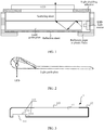
- a structure may be shown in FIG. 1 , where light emitted from the LED light source is converted into planar light after transported by the light guide plate, and after passing through a scattering sheet, the light comes out vertically to the LCD.
- an LED-embedded light guide plate is further put forward in the industry to improve the amount of incident light, as shown in FIG. 2 .
- a requirement on a thickness of the LCM is increasingly high.
- the light guide plate is required to become thinner.
- a miniaturization speed of the LED is slower than a thinning speed of the LCM, which leads to a case in which the thickness of the light guide plate is close to the thickness of the LED, and even the thickness of the light guide plate is less than the thickness of the LED. Therefore, a structure of the LED-embedded light guide plate restrains the development of the LCM thinning.
- Embodiments of the present invention provide a light guide plate, a liquid crystal display module, and a terminal device, which can improve the amount of incident light of a light guide plate and increase backlight efficiency of an LCM without increasing a size of the LCM.
- an embodiment of the present invention provides a light guide plate, including:
- the light inlet surface further includes a groove peripheral surface of the first groove.
- the first groove is further configured to form airtight space with the first light source, so as to prevent the light emitted from the first light source from coming out from another place except the light inlet surface.
- the bottom surface is planar or arc-shaped.
- the first groove is disposed on an end of an upper surface or an end of a lower surface of the light guide plate substrate; and an angle between the groove peripheral surface of the first groove and the upper surface or the lower surface is a right angle.
- the first groove is disposed on a joint of an upper surface and an end surface of the light guide plate substrate, or the first groove is disposed on a joint of a lower surface and an end surface of the light guide plate substrate; and an angle between the groove peripheral surface of the first groove and the upper surface or the lower surface of the light guide plate substrate is an acute angle.
- the joint of the upper surface or the lower surface of the light guide plate substrate and the end surface of the light guide plate substrate is a curved surface.
- optical clear adhesive is filled between the light emitting portion of the first light source and the first groove.
- the light reflection layer is any one of silver, aluminum, and non-metallic dielectric film, where the non-metallic dielectric film is made of silicon dioxide and titanium oxide, or silicon dioxide and niobium oxide.
- the light reflection layer is disposed on the part of the outer surface of the light guide plate substrate except the light inlet surface and the light outlet surface by means of any process of electroplating, vacuum electroplating, sputtering, electrophoresis, and coating.
- the first light source includes any one of an inorganic LED, an organic LED, electroluminescence, photoluminescence, quantum luminescence, and laser.
- an embodiment of the present invention provides a liquid crystal display module, including a light guide plate, a first light source, a scattering sheet, a liquid crystal display, and a drive circuit
- the light guide plate includes: a light guide plate substrate and a light reflection layer, where the light guide plate substrate includes a light inlet surface and a light outlet surface, a first groove is disposed on the light guide plate substrate, the first groove is configured to accommodate a light emitting portion of the first light source, a bottom surface of the first groove forms the light inlet surface, and the light reflection layer is disposed on a part of an outer surface of the light guide plate substrate except the light inlet surface and the light outlet surface; light emitted from the first light source enters the light guide plate substrate through the light inlet surface, and is refracted by the light reflection layer, so that the light emitted from the first light source comes out through the light outlet surface; and the scattering sheet is located on the light outlet surface of the light guide plate, the liquid crystal display is located on the scatter
- the light inlet surface further includes a groove peripheral surface of the first groove.
- the first groove is further configured to form airtight space with the first light source, so as to prevent the light emitted from the first light source from coming out from another place except the light inlet surface.
- the bottom surface is planar or arc-shaped.
- the first groove is disposed on an end of an upper surface or an end of a lower surface of the light guide plate substrate; and an angle between the groove peripheral surface of the first groove and the upper surface or the lower surface is a right angle.
- the first groove is disposed on a joint of an upper surface and an end surface of the light guide plate substrate, or the first groove is disposed on a joint of a lower surface and an end surface of the light guide plate substrate; and an angle between the groove peripheral surface of the first groove and the upper surface or the lower surface of the light guide plate substrate is an acute angle.
- the joint of the upper surface or the lower surface of the light guide plate substrate and the end surface of the light guide plate substrate is a curved surface.
- optical clear adhesive is filled between the light emitting portion of the first light source and the first groove.
- the light reflection layer is any one of silver, aluminum, and non-metallic dielectric film, where the non-metallic dielectric film is made of silicon dioxide and titanium oxide, or silicon dioxide and niobium oxide.
- the light reflection layer is disposed on the part of the outer surface of the light guide plate substrate except the light inlet surface and the light outlet surface by means of any process of electroplating, vacuum electroplating, sputtering, electrophoresis, and coating.
- the scattering sheet in a tenth possible implementation manner, includes a scattering film and an antireflective film, where the scattering film is located on the light outlet surface of the light guide plate, and the antireflective film is located on the scattering film; or the scattering sheet includes a scattering film, where the scattering film is located on the light outlet surface of the light guide plate.
- an embodiment of the present invention provides a terminal device, including the liquid crystal display module described in the second aspect.
- the terminal device further includes a flexible printed circuit board, and the liquid crystal display module receives image data by using the flexible printed circuit board.
- a light reflection layer on a part of a light guide plate substrate except a light inlet surface and a light outlet surface increases reflection efficiency of a light guide plate
- a first groove on the light guide plate substrate accommodates a light emitting portion of a first light source, so that the first light source is partially embedded in the first groove, effectively improving the amount of incident light of the light guide plate. In this way, backlight efficiency of an LCM is improved without increasing a size of the LCM.
- a light guide plate, a liquid crystal display module, and a terminal device provided in embodiments of the present invention are described below in detail.
- FIG. 3 is a schematic diagram of a light guide plate according to an embodiment of the present invention.
- the light guide plate 1 includes a light guide plate substrate 11 and a light reflection layer 12, where the light guide plate substrate 11 includes a light inlet surface 112 and a light outlet surface 113, where a first groove 111 is disposed on the light guide plate substrate 11, the first groove 111 is configured to accommodate a light emitting portion of a first light source, and a bottom surface 1112 of the first groove 111 forms the light inlet surface 112; and the light reflection layer 12 is disposed on a part of an outer surface of the light guide plate substrate 11 except the light inlet surface 112 and the light outlet surface 113, where after light emitted from the first light source enters the light guide plate substrate 11 through the light inlet surface 112, and is refracted by the light reflection layer 12, the light emitted from the first light source comes out through the light outlet surface 113.
- the first groove 111 accommodates the light emitting portion of the first light source
- the light reflection layer is disposed on the part of the outer surface of the light guide plate substrate except the light inlet surface 112 and the light outlet surface 113, so that after light emitted from the light emitting portion of the first light source enters the light guide plate substrate 11 through the light inlet surface 112, and is refracted by the light reflection layer 12, the light emitted from the first light source can be output through the light outlet surface 113, so as to prevent light in the light guide plate 1 from coming out from another place and affecting light guiding efficiency of the light guide plate 1.
- the bottom surface 1112 of the first groove 111 may be planar or arc-shaped.
- the light inlet surface 112 may further include a groove peripheral surface 1111 of the first groove 111, and a cross section of the groove peripheral surface 1111 may be rectangular or circular, or in another shape.
- the first groove 111 when the bottom surface 1112 of the first groove 111 is arc-shaped, in this case, the first groove 111 may not have the groove peripheral surface 1111; certainly, when the bottom surface 1112 of the first groove 111 is arc-shaped, the first groove 111 may also have the groove peripheral surface 1111.
- the first groove 111 may form airtight space with the first light source, so as to prevent the light emitted from the first light source from coming out from another place except the light inlet surface 112.
- the first light source may be an LED light source, or may be another light source.
- the first light source may include but is not limited to any one of an inorganic LED, an organic LED, electroluminescence, photoluminescence, quantum luminescence, and laser, or may be a light source generating light indirectly and passively or a light source generating light directly.
- An LED light source is used as an example for a specific description below.
- the first groove 111 is disposed on an end of an upper surface or an end of a lower surface of the light guide plate substrate 11; and an angle between the groove peripheral surface 1111 of the first groove 111 and the upper surface or the lower surface of the light guide plate substrate 11 may be an acute angle or a right angle (that is, an angle between a direction of a peripheral surface of the first groove 111 and the lower surface or the upper surface of the light guide plate substrate 11 may be an acute angle or a right angle).
- the first groove 111 is disposed on a joint of an upper surface and an end surface of the light guide plate substrate 11, or the first groove 111 is disposed on a joint of a lower surface and an end surface of the light guide plate substrate 11; and an angle between the groove peripheral surface 1111 of the first groove 111 and the upper surface or the lower surface of the light guide plate substrate 11 is an acute angle (that is, an angle between a direction of a peripheral surface of the first groove 111 and the upper surface or the lower surface of the light guide plate substrate 11 may be an acute angle or a right angle).
- FIG. 3 shows a case in which the angle between the groove peripheral surface 1111 of the first groove 111 and the lower surface of the light guide plate substrate 11 is a right angle.
- the light guide plate 1 is required to be relatively thin, and therefore a position of the first groove 111 may be changed, as shown in FIG. 4 .
- the angle between the groove peripheral surface 1111 of the first groove 111 and the lower surface of the light guide plate substrate 11 is an acute angle (that is, the angle between the direction of the peripheral surface of the first groove 111 and the lower surface of the light guide plate substrate 11 may be an acute angle or a right angle), and the first groove 111 is disposed on the joint of the lower surface and the end surface of the light guide plate substrate 11.
- a case in which the first groove 111 is disposed on the upper surface of the light guide plate substrate 11 is similar to that in FIG. 3 , which is not shown individually.
- the angle between the groove peripheral surface 1111 of the first groove 111 and the upper surface or the lower surface of the light guide plate substrate 11 may be preferably between 80° and 90°.
- a joint of a surface (for example, the upper surface of the light guide plate substrate 11) opposite to a surface on which the first groove 111 is located (for example, the lower surface of the light guide plate substrate 11) on the light guide plate substrate 11 and an end surface of the light guide plate substrate 11 (that is, a side surface of the light guide plate substrate 11) is a curved surface, which can enhance reflection of the light emitted from the light emitting portion of the LED light source in the first groove 111, and improve light guiding efficiency of the light guide plate substrate 11.
- the LED light source is partially embedded in the first groove 111, that is, after the light emitting portion of the LED light source is disposed in the first groove 111, a gap between the light emitting portion of the LED light source and the first groove 111 may be filled with optical clear adhesive (which is not shown in a figure), to decrease losses of light reflection and scattering caused by an air gap.
- the first groove 111 of the light guide plate substrate 11 accommodates the light emitting portion of the first light source, so that the first light source is partially embedded in the first groove 111, which effectively improves the amount of incident light of the light guide plate without increasing a thickness of the light guide plate.
- the light reflection layer 12 may be made of a metal material having a good reflection effect, such as silver or aluminum, or may be a dielectric film made of other non-metallic materials having a good reflection effect.
- the non-metallic materials may be silicon dioxide and titanium oxide, or silicon dioxide and niobium oxide.
- the light reflection layer 12 may be disposed at all or some positions on the outer surface of the light guide plate substrate 11 except the light inlet surface 112 and the light outlet surface 113 by means of any process of electroplating, vacuum electroplating, sputtering, electrophoresis, and coating.
- This structure is applicable to light guide plates in different manners of light input by a light source, for example, the structure may be used for a light guide plate in an LED backlight manner in this embodiment of the present invention, and may also be used for another light guide plate in another light output manner; and the structure may be used for a light guide plate of an LED light source, and may also be used for another light guide plate of another light source.
- the light reflection layer 12 is disposed on the outer surface of the light guide plate substrate 11 except the light inlet surface 112 and the light outlet surface 113.
- usage of the light reflection layer 12 not only effectively reduces light losses and reflection decrease caused by an air gap, but also effectively reduces a thickness and length of the light guide plate substrate 11.
- an embodiment of the present invention provides a liquid crystal display module (LCM) to which the light guide plate provided in the foregoing embodiment is applied.
- the LCM includes: a light guide plate 1, a first light source 2, a scattering sheet 3, a liquid crystal display (LCD) 4, and a drive circuit 6.
- the light guide plate 1 includes a light guide plate substrate 11 and a light reflection layer 12, where the light guide plate substrate 11 includes a light inlet surface 112 and a light outlet surface 113, where the first groove 111 is configured to accommodate a light emitting portion 21 of a first light source, and a bottom surface 1112 of the first groove 111 forms the light inlet surface 112; the light reflection layer 12 is disposed on a part of an outer surface of the light guide plate substrate 11 except the light inlet surface 112 and the light outlet surface 113; after light emitted from the first light source 2 enters the light guide plate substrate 11 through the light inlet surface 112, and is refracted by the light reflection layer 12, the light emitted from the first light source 2 comes out through the light outlet surface 113; the scattering sheet 3 is located on the light outlet surface 113 of the light guide plate 1, and the LCD 4 is located on the scattering sheet 3; and the drive circuit 6 is electrically connected to the LCD 4.
- the first groove 111 accommodates the light emitting portion 21 of the first light source 2, and the light reflection layer 12 is disposed on the part of the outer surface of the light guide plate substrate 11 except the light inlet surface 112 and the light outlet surface 113, so that after light emitted from the light emitting portion 21 of the first light source 2 enters the light guide plate substrate 11 through the light inlet surface 112, and is refracted by the light reflection layer 12, the light emitted from the first light source 2 can be output through the light outlet surface 113, so as to prevent light in the light guide plate 1 from coming out from another place and affecting light guiding efficiency of the light guide plate 1.
- the bottom surface 1112 of the first groove 111 may be planar or arc-shaped.
- the light inlet surface 112 may further include a groove peripheral surface 1111 of the first groove 111, and a cross section of the groove peripheral surface 1111 may be rectangular or circular, or in another shape.
- the first groove 111 may form airtight space with the first light source, so as to prevent the light emitted from the first light source from coming out from another place except the light inlet surface 112.
- the first groove 111 is disposed on an end of a lower surface or an upper surface of the light guide plate substrate 11; and an angle between the groove peripheral surface 1111 of the first groove 111 and the lower surface or the upper surface of the light guide plate substrate 11 may be an acute angle or a right angle.
- the first groove 111 is disposed on a joint of an upper surface and an end surface of the light guide plate substrate 11, or the first groove 111 is disposed on a joint of a lower surface and an end surface of the light guide plate substrate 11; and an angle between the groove peripheral surface 1111 of the first groove 111 and the upper surface or the lower surface of the light guide plate substrate 11 is an acute angle.
- the first light source 2 may be an LED light source.
- the light emitting portion 21 of the first light source 2 is embedded in the first groove 111 of the light guide plate 1, and a gap between the light emitting portion 21 of the first light source 2 and the first groove 111 of the light guide plate 1 may be filled with optical clear adhesive 114.
- the rest part of the first light source 2 may be disposed outside the light guide plate 1. All of the light emitted from the light emitting portion 21 of the LED light source 2 almost enters the light guide plate 1, comes out through the light outlet surface (which is not shown in FIG. 5 ) of the light guide plate 1 after refracted by the light reflection layer 12 in the light guide plate 1, and enters the scattering sheet 3 disposed on the light outlet surface of the light guide plate 1.
- the scattering sheet 3 scatters the received light, and the light is finally output through the LCD 4 disposed on the scattering sheet 3.
- the scattering sheet 3 may include a scattering film and an antireflective film, where the scattering film is located on the light outlet surface 113 of the light guide plate 1, and the antireflective film is located on the scattering film.
- the scattering sheet 3 may also include a scattering film, where the scattering film is located on the light outlet surface 113 of the light guide plate 1.
- the drive circuit 6 may be a driver IC, and may be welded on the LCD 4 for electrical connection to the LCD 4.
- the LCM may further include a flexible printed circuit board (Flexible Printed Circuit Board, FPC) 5, and the LCM may receive, by using the FPC 5, image data sent by a processor of a terminal device on which the LCM is located.
- FPC Flexible Printed Circuit Board
- the LCD 4 may include multiple liquid crystal pixels, and each liquid crystal pixel includes three elements: R, G, and B.
- the LCM receives the image data by using the FPC 5, and sends the image data to the driver IC.
- the driver IC has a memory (for example, a random access memory), which can store the image data, and the driver IC outputs a corresponding voltage signal to each liquid crystal pixel on the LCD 4 according to the image data.
- Corresponding liquid crystal deflection is performed for the liquid crystal pixel of the LCD 4 according to the received voltage signal, where different voltage values determine different liquid crystal deflection angles, so that the liquid crystal pixels are displayed with different luminance degrees and colors by using different liquid crystal deflection angles. In this way, the LCM can display the received image data.
- an angle between the groove peripheral surface of the first groove 111 and a bottom surface of the light guide plate 1 may be an acute angle.
- the bottom surface of the light guide plate 1 is a lower surface of the light guide plate 1.
- an angle between the groove peripheral surface of the first groove 111 and a bottom surface of the light guide plate 1 may be a right angle.
- the bottom surface of the light guide plate 1 is a lower surface of the light guide plate 1.
- a thickness of an end of the light guide plate 1 on which the first groove 111 is located is equal to a thickness of the rest part of the light guide plate 1.
- a thickness of an end of the light guide plate 1 on which the first groove 111 is located is greater than a thickness of the rest part of the light guide plate 1.
- a solution in which the gap between the light emitting portion 21 of the LED light source 2 and the first groove 111 of the light guide plate 1 is filled with the optical clear adhesive 114 is provided, to implement exclusion of an air gap between the light guide plate 1 and the LED light source 2.
- the light guide plate 1 and the LED light source 2 may be integrally formed by injection molding or another manner may be used to implement exclusion of an air gap between the light guide plate 1 and the LED light source 2.
- the light reflection layer 12 on the light guide plate 1 increases reflection efficiency of the light guide plate 1, and the first groove 111 on the light guide plate accommodates the light emitting portion 21 of the first light source 2, so that the light emitting portion 21 of the first light source 2 is embedded in the first groove 111, effectively improving the amount of incident light of the light guide plate 1.
- backlight efficiency of the LCM is improved without increasing a size of the LCM.
- an embodiment of the present invention further provides a terminal device, including the liquid crystal display module provided in the foregoing embodiment.
- the terminal device may be a terminal having a liquid crystal display module, for example, the terminal device may be a cell phone, a wearable device, a navigator, a computer, or a PAD.
Landscapes
- Physics & Mathematics (AREA)
- General Physics & Mathematics (AREA)
- Optics & Photonics (AREA)
- Nonlinear Science (AREA)
- Engineering & Computer Science (AREA)
- Microelectronics & Electronic Packaging (AREA)
- Mathematical Physics (AREA)
- Chemical & Material Sciences (AREA)
- Crystallography & Structural Chemistry (AREA)
- Planar Illumination Modules (AREA)
- Liquid Crystal (AREA)
- Light Guides In General And Applications Therefor (AREA)
Abstract
Description
- The present invention relates to the liquid crystal display field, and in particular, to a light guide plate, a liquid crystal display module, and a terminal device.
- Because a liquid crystal module of a liquid crystal display does not emit light itself, to enable the liquid crystal display to normally display an image, a backlight module is used to provide enough luminance and a uniformly distributed light source to display the image. The backlight module is one of key components of a liquid crystal display module (liquid crystal display module, LCM). At present, a liquid crystal display (liquid crystal display module, LCD) panel made by using the LCM has been widely used in electronics products, such as a display, a notebook computer, a cell phone, a digital camera, and a projector.
- A light guide plate is one important part of the LCM, and performance of the light guide plate severely restrains backlight efficiency of the LCM. For a small-sized LCM, an existing backlight light source is generally an edge-illumination type backlight light source. However, because an LED light source is disposed outside the light guide plate, a gap exists between the LED light source and the light guide plate; as a result, light of the LED is caused to leak from surrounding edges and a back side of the light guide plate, leading to low backlight efficiency.
- An existing solution is to add a reflection paper or use a white plastic frame at the periphery of the light guide plate to reflect, add a reflection sheet to the back side, and apply light shielding adhesive to a gap between the top side and the LCD. A structure may be shown in
FIG. 1 , where light emitted from the LED light source is converted into planar light after transported by the light guide plate, and after passing through a scattering sheet, the light comes out vertically to the LCD. However, using a reflection paper or a white plastic frame to reflect light undoubtedly brings about a space occupation problem, and increases a size of the LCM and costs; in addition, there is an air gap between the reflection paper or the white plastic frame and the light guide plate, which causes a light leakage phenomenon and decreases the quality of the LCM. - In addition, an LED-embedded light guide plate is further put forward in the industry to improve the amount of incident light, as shown in
FIG. 2 . However, with the development of a thinning tendency of products, such as a cell phone and a PAD, a requirement on a thickness of the LCM is increasingly high. To reduce the thickness of the LCM, the light guide plate is required to become thinner. A miniaturization speed of the LED is slower than a thinning speed of the LCM, which leads to a case in which the thickness of the light guide plate is close to the thickness of the LED, and even the thickness of the light guide plate is less than the thickness of the LED. Therefore, a structure of the LED-embedded light guide plate restrains the development of the LCM thinning. - Embodiments of the present invention provide a light guide plate, a liquid crystal display module, and a terminal device, which can improve the amount of incident light of a light guide plate and increase backlight efficiency of an LCM without increasing a size of the LCM.
- According to a first aspect, an embodiment of the present invention provides a light guide plate, including:
- a light guide plate substrate, including a light inlet surface and a light outlet surface, where a first groove is disposed on the light guide plate substrate, the first groove is configured to accommodate a light emitting portion of a first light source, and a bottom surface of the first groove forms the light inlet surface; and
- a light reflection layer, disposed on a part of an outer surface of the light guide plate substrate except the light inlet surface and the light outlet surface, where
- light emitted from the first light source enters the light guide plate substrate through the light inlet surface, and is refracted by the light reflection layer, so that the light emitted from the first light source comes out through the light outlet surface.
- In a first possible implementation manner, the light inlet surface further includes a groove peripheral surface of the first groove.
- With reference to the first aspect or the first possible implementation manner of the first aspect, in a second possible implementation manner, the first groove is further configured to form airtight space with the first light source, so as to prevent the light emitted from the first light source from coming out from another place except the light inlet surface.
- In a third possible implementation manner, the bottom surface is planar or arc-shaped.
- With reference to the first possible implementation manner of the first aspect, in a fourth possible implementation manner, the first groove is disposed on an end of an upper surface or an end of a lower surface of the light guide plate substrate; and an angle between the groove peripheral surface of the first groove and the upper surface or the lower surface is a right angle.
- With reference to the first possible implementation manner of the first aspect, in a fifth possible implementation manner, the first groove is disposed on a joint of an upper surface and an end surface of the light guide plate substrate, or the first groove is disposed on a joint of a lower surface and an end surface of the light guide plate substrate; and an angle between the groove peripheral surface of the first groove and the upper surface or the lower surface of the light guide plate substrate is an acute angle.
- With reference to the first aspect or the fourth or fifth possible implementation manner of the first aspect, in a sixth possible implementation manner, the joint of the upper surface or the lower surface of the light guide plate substrate and the end surface of the light guide plate substrate is a curved surface.
- With reference to the first aspect or the first, second, third, fourth, fifth, or sixth possible implementation manner of the first aspect, in a seventh possible implementation manner, optical clear adhesive is filled between the light emitting portion of the first light source and the first groove.
- With reference to the first aspect or the first, second, third, fourth, fifth, sixth, or seventh possible implementation manner of the first aspect, in an eighth possible implementation manner, the light reflection layer is any one of silver, aluminum, and non-metallic dielectric film, where
the non-metallic dielectric film is made of silicon dioxide and titanium oxide, or silicon dioxide and niobium oxide. - With reference to the first aspect or the first, second, third, fourth, fifth, sixth, seventh, or eighth possible implementation manner of the first aspect, in a ninth possible implementation manner, the light reflection layer is disposed on the part of the outer surface of the light guide plate substrate except the light inlet surface and the light outlet surface by means of any process of electroplating, vacuum electroplating, sputtering, electrophoresis, and coating.
- With reference to the first aspect or the first, second, third, fourth, fifth, sixth, seventh, eighth, or ninth possible implementation manner of the first aspect, in a tenth possible implementation manner, the first light source includes any one of an inorganic LED, an organic LED, electroluminescence, photoluminescence, quantum luminescence, and laser.
- According to a second aspect, an embodiment of the present invention provides a liquid crystal display module, including a light guide plate, a first light source, a scattering sheet, a liquid crystal display, and a drive circuit, where
the light guide plate includes: a light guide plate substrate and a light reflection layer, where the light guide plate substrate includes a light inlet surface and a light outlet surface, a first groove is disposed on the light guide plate substrate, the first groove is configured to accommodate a light emitting portion of the first light source, a bottom surface of the first groove forms the light inlet surface, and the light reflection layer is disposed on a part of an outer surface of the light guide plate substrate except the light inlet surface and the light outlet surface;
light emitted from the first light source enters the light guide plate substrate through the light inlet surface, and is refracted by the light reflection layer, so that the light emitted from the first light source comes out through the light outlet surface; and
the scattering sheet is located on the light outlet surface of the light guide plate, the liquid crystal display is located on the scattering sheet, and the drive circuit is electrically connected to the liquid crystal display. - In a first possible implementation manner, the light inlet surface further includes a groove peripheral surface of the first groove.
- With reference to the second aspect or the first possible implementation manner of the second aspect, in a second possible implementation manner, the first groove is further configured to form airtight space with the first light source, so as to prevent the light emitted from the first light source from coming out from another place except the light inlet surface.
- With reference to the first or second possible implementation manner of the second aspect, in a third possible implementation manner, the bottom surface is planar or arc-shaped.
- With reference to the second aspect or the first possible implementation manner of the second aspect, in a fourth possible implementation manner, the first groove is disposed on an end of an upper surface or an end of a lower surface of the light guide plate substrate; and an angle between the groove peripheral surface of the first groove and the upper surface or the lower surface is a right angle.
- With reference to the second aspect or the first possible implementation manner of the second aspect, in a fifth possible implementation manner, the first groove is disposed on a joint of an upper surface and an end surface of the light guide plate substrate, or the first groove is disposed on a joint of a lower surface and an end surface of the light guide plate substrate; and an angle between the groove peripheral surface of the first groove and the upper surface or the lower surface of the light guide plate substrate is an acute angle.
- With reference to the fourth or fifth possible implementation manner of the second aspect, in a sixth possible implementation manner, the joint of the upper surface or the lower surface of the light guide plate substrate and the end surface of the light guide plate substrate is a curved surface.
- With reference to the second aspect or the first, second, third, fourth, fifth, or sixth possible implementation manner of the second aspect, in a seventh possible implementation manner, optical clear adhesive is filled between the light emitting portion of the first light source and the first groove.
- With reference to the second aspect or the first, second, third, fourth, fifth, sixth, or seventh possible implementation manner of the second aspect, in an eighth possible implementation manner, the light reflection layer is any one of silver, aluminum, and non-metallic dielectric film, where
the non-metallic dielectric film is made of silicon dioxide and titanium oxide, or silicon dioxide and niobium oxide. - With reference to the second aspect or the first, second, third, fourth, fifth, sixth, seventh, or eighth possible implementation manner of the second aspect, in a ninth possible implementation manner, the light reflection layer is disposed on the part of the outer surface of the light guide plate substrate except the light inlet surface and the light outlet surface by means of any process of electroplating, vacuum electroplating, sputtering, electrophoresis, and coating.
- With reference to the second aspect or the first, second, third, fourth, fifth, sixth, seventh, eighth, or ninth possible implementation manner of the second aspect, in a tenth possible implementation manner, the scattering sheet includes a scattering film and an antireflective film, where the scattering film is located on the light outlet surface of the light guide plate, and the antireflective film is located on the scattering film; or
the scattering sheet includes a scattering film, where the scattering film is located on the light outlet surface of the light guide plate. - According to a third aspect, an embodiment of the present invention provides a terminal device, including the liquid crystal display module described in the second aspect.
- In a first possible implementation manner, the terminal device further includes a flexible printed circuit board, and the liquid crystal display module receives image data by using the flexible printed circuit board.
- According to a light guide plate, a liquid crystal display module, and a terminal device in the embodiments of the present invention, a light reflection layer on a part of a light guide plate substrate except a light inlet surface and a light outlet surface increases reflection efficiency of a light guide plate, and a first groove on the light guide plate substrate accommodates a light emitting portion of a first light source, so that the first light source is partially embedded in the first groove, effectively improving the amount of incident light of the light guide plate. In this way, backlight efficiency of an LCM is improved without increasing a size of the LCM.
-
-
FIG. 1 is a schematic diagram of an LCM according to the prior art; -
FIG. 2 is a schematic diagram of an LED-embedded light guide plate according to the prior art; -
FIG. 3 is a schematic sectional view of a light guide plate according to an embodiment of the present invention; -
FIG. 4 is a schematic sectional view of another light guide plate according to an embodiment of the present invention; and -
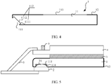
FIG. 5 is a schematic structural diagram of an LCM according to an embodiment of the present invention. - A light guide plate, a liquid crystal display module, and a terminal device provided in embodiments of the present invention are described below in detail.
-
FIG. 3 is a schematic diagram of a light guide plate according to an embodiment of the present invention. - As shown in
FIG. 3 , thelight guide plate 1 provided in this embodiment of the present invention includes a lightguide plate substrate 11 and alight reflection layer 12, where
the lightguide plate substrate 11 includes alight inlet surface 112 and alight outlet surface 113, where afirst groove 111 is disposed on the lightguide plate substrate 11, thefirst groove 111 is configured to accommodate a light emitting portion of a first light source, and abottom surface 1112 of thefirst groove 111 forms thelight inlet surface 112; and
thelight reflection layer 12 is disposed on a part of an outer surface of the lightguide plate substrate 11 except thelight inlet surface 112 and thelight outlet surface 113, where
after light emitted from the first light source enters the lightguide plate substrate 11 through thelight inlet surface 112, and is refracted by thelight reflection layer 12, the light emitted from the first light source comes out through thelight outlet surface 113. - It can been seen from above that the
first groove 111 accommodates the light emitting portion of the first light source, and the light reflection layer is disposed on the part of the outer surface of the light guide plate substrate except thelight inlet surface 112 and thelight outlet surface 113, so that after light emitted from the light emitting portion of the first light source enters the lightguide plate substrate 11 through thelight inlet surface 112, and is refracted by thelight reflection layer 12, the light emitted from the first light source can be output through thelight outlet surface 113, so as to prevent light in thelight guide plate 1 from coming out from another place and affecting light guiding efficiency of thelight guide plate 1. - The
bottom surface 1112 of thefirst groove 111 may be planar or arc-shaped. - Optionally, the
light inlet surface 112 may further include a grooveperipheral surface 1111 of thefirst groove 111, and a cross section of the grooveperipheral surface 1111 may be rectangular or circular, or in another shape. - It should be noted that, in this embodiment of the present invention, when the
bottom surface 1112 of thefirst groove 111 is arc-shaped, in this case, thefirst groove 111 may not have the grooveperipheral surface 1111; certainly, when thebottom surface 1112 of thefirst groove 111 is arc-shaped, thefirst groove 111 may also have the grooveperipheral surface 1111. - The
first groove 111 may form airtight space with the first light source, so as to prevent the light emitted from the first light source from coming out from another place except thelight inlet surface 112. - The first light source may be an LED light source, or may be another light source. The first light source may include but is not limited to any one of an inorganic LED, an organic LED, electroluminescence, photoluminescence, quantum luminescence, and laser, or may be a light source generating light indirectly and passively or a light source generating light directly.
- An LED light source is used as an example for a specific description below.
- The
first groove 111 is disposed on an end of an upper surface or an end of a lower surface of the lightguide plate substrate 11; and an angle between the grooveperipheral surface 1111 of thefirst groove 111 and the upper surface or the lower surface of the lightguide plate substrate 11 may be an acute angle or a right angle (that is, an angle between a direction of a peripheral surface of thefirst groove 111 and the lower surface or the upper surface of the lightguide plate substrate 11 may be an acute angle or a right angle). Alternatively, thefirst groove 111 is disposed on a joint of an upper surface and an end surface of the lightguide plate substrate 11, or thefirst groove 111 is disposed on a joint of a lower surface and an end surface of the lightguide plate substrate 11; and an angle between the grooveperipheral surface 1111 of thefirst groove 111 and the upper surface or the lower surface of the lightguide plate substrate 11 is an acute angle (that is, an angle between a direction of a peripheral surface of thefirst groove 111 and the upper surface or the lower surface of the lightguide plate substrate 11 may be an acute angle or a right angle). - Specifically,
FIG. 3 shows a case in which the angle between the grooveperipheral surface 1111 of thefirst groove 111 and the lower surface of the lightguide plate substrate 11 is a right angle. - In some products, the
light guide plate 1 is required to be relatively thin, and therefore a position of thefirst groove 111 may be changed, as shown inFIG. 4 . The angle between the grooveperipheral surface 1111 of thefirst groove 111 and the lower surface of the lightguide plate substrate 11 is an acute angle (that is, the angle between the direction of the peripheral surface of thefirst groove 111 and the lower surface of the lightguide plate substrate 11 may be an acute angle or a right angle), and thefirst groove 111 is disposed on the joint of the lower surface and the end surface of the lightguide plate substrate 11. - A case in which the
first groove 111 is disposed on the upper surface of the lightguide plate substrate 11 is similar to that inFIG. 3 , which is not shown individually. - As restraint between a size of the LED light source and a thickness of the light guide plate is considered, the angle between the groove
peripheral surface 1111 of thefirst groove 111 and the upper surface or the lower surface of the lightguide plate substrate 11 may be preferably between 80° and 90°. - As shown in
FIG. 3 , a joint of a surface (for example, the upper surface of the light guide plate substrate 11) opposite to a surface on which thefirst groove 111 is located (for example, the lower surface of the light guide plate substrate 11) on the lightguide plate substrate 11 and an end surface of the light guide plate substrate 11 (that is, a side surface of the light guide plate substrate 11) is a curved surface, which can enhance reflection of the light emitted from the light emitting portion of the LED light source in thefirst groove 111, and improve light guiding efficiency of the lightguide plate substrate 11. - The LED light source is partially embedded in the
first groove 111, that is, after the light emitting portion of the LED light source is disposed in thefirst groove 111, a gap between the light emitting portion of the LED light source and thefirst groove 111 may be filled with optical clear adhesive (which is not shown in a figure), to decrease losses of light reflection and scattering caused by an air gap. - Therefore, the
first groove 111 of the lightguide plate substrate 11 accommodates the light emitting portion of the first light source, so that the first light source is partially embedded in thefirst groove 111, which effectively improves the amount of incident light of the light guide plate without increasing a thickness of the light guide plate. - The
light reflection layer 12 may be made of a metal material having a good reflection effect, such as silver or aluminum, or may be a dielectric film made of other non-metallic materials having a good reflection effect. The non-metallic materials may be silicon dioxide and titanium oxide, or silicon dioxide and niobium oxide. Thelight reflection layer 12 may be disposed at all or some positions on the outer surface of the lightguide plate substrate 11 except thelight inlet surface 112 and thelight outlet surface 113 by means of any process of electroplating, vacuum electroplating, sputtering, electrophoresis, and coating. This structure is applicable to light guide plates in different manners of light input by a light source, for example, the structure may be used for a light guide plate in an LED backlight manner in this embodiment of the present invention, and may also be used for another light guide plate in another light output manner; and the structure may be used for a light guide plate of an LED light source, and may also be used for another light guide plate of another light source. - The
light reflection layer 12 is disposed on the outer surface of the lightguide plate substrate 11 except thelight inlet surface 112 and thelight outlet surface 113. Compared with conventional usage of an adhesive material, for example, a manner of using a reflection paper, a white plastic frame, or a reflection sheet, usage of thelight reflection layer 12 not only effectively reduces light losses and reflection decrease caused by an air gap, but also effectively reduces a thickness and length of the lightguide plate substrate 11. - Correspondingly, an embodiment of the present invention provides a liquid crystal display module (LCM) to which the light guide plate provided in the foregoing embodiment is applied. As shown in
FIG. 5 , the LCM includes: alight guide plate 1, a firstlight source 2, ascattering sheet 3, a liquid crystal display (LCD) 4, and adrive circuit 6. - Referring to
FIG. 3 again, thelight guide plate 1 includes a lightguide plate substrate 11 and alight reflection layer 12, where
the lightguide plate substrate 11 includes alight inlet surface 112 and alight outlet surface 113, where thefirst groove 111 is configured to accommodate alight emitting portion 21 of a first light source, and abottom surface 1112 of thefirst groove 111 forms thelight inlet surface 112;
thelight reflection layer 12 is disposed on a part of an outer surface of the lightguide plate substrate 11 except thelight inlet surface 112 and thelight outlet surface 113;
after light emitted from the firstlight source 2 enters the lightguide plate substrate 11 through thelight inlet surface 112, and is refracted by thelight reflection layer 12, the light emitted from the firstlight source 2 comes out through thelight outlet surface 113;
thescattering sheet 3 is located on thelight outlet surface 113 of thelight guide plate 1, and theLCD 4 is located on thescattering sheet 3; and
thedrive circuit 6 is electrically connected to theLCD 4. - It can been seen from above that, in the liquid crystal display module (LCM) in this embodiment, the
first groove 111 accommodates thelight emitting portion 21 of the firstlight source 2, and thelight reflection layer 12 is disposed on the part of the outer surface of the lightguide plate substrate 11 except thelight inlet surface 112 and thelight outlet surface 113, so that after light emitted from thelight emitting portion 21 of the firstlight source 2 enters the lightguide plate substrate 11 through thelight inlet surface 112, and is refracted by thelight reflection layer 12, the light emitted from the firstlight source 2 can be output through thelight outlet surface 113, so as to prevent light in thelight guide plate 1 from coming out from another place and affecting light guiding efficiency of thelight guide plate 1. - The
bottom surface 1112 of thefirst groove 111 may be planar or arc-shaped. - Optionally, the
light inlet surface 112 may further include a grooveperipheral surface 1111 of thefirst groove 111, and a cross section of the grooveperipheral surface 1111 may be rectangular or circular, or in another shape. - The
first groove 111 may form airtight space with the first light source, so as to prevent the light emitted from the first light source from coming out from another place except thelight inlet surface 112. - The
first groove 111 is disposed on an end of a lower surface or an upper surface of the lightguide plate substrate 11; and an angle between the grooveperipheral surface 1111 of thefirst groove 111 and the lower surface or the upper surface of the lightguide plate substrate 11 may be an acute angle or a right angle. Alternatively, thefirst groove 111 is disposed on a joint of an upper surface and an end surface of the lightguide plate substrate 11, or thefirst groove 111 is disposed on a joint of a lower surface and an end surface of the lightguide plate substrate 11; and an angle between the grooveperipheral surface 1111 of thefirst groove 111 and the upper surface or the lower surface of the lightguide plate substrate 11 is an acute angle. - The first
light source 2 may be an LED light source. Thelight emitting portion 21 of the firstlight source 2 is embedded in thefirst groove 111 of thelight guide plate 1, and a gap between thelight emitting portion 21 of the firstlight source 2 and thefirst groove 111 of thelight guide plate 1 may be filled with opticalclear adhesive 114. The rest part of the firstlight source 2 may be disposed outside thelight guide plate 1. All of the light emitted from thelight emitting portion 21 of the LEDlight source 2 almost enters thelight guide plate 1, comes out through the light outlet surface (which is not shown inFIG. 5 ) of thelight guide plate 1 after refracted by thelight reflection layer 12 in thelight guide plate 1, and enters thescattering sheet 3 disposed on the light outlet surface of thelight guide plate 1. Thescattering sheet 3 scatters the received light, and the light is finally output through theLCD 4 disposed on thescattering sheet 3. - The
scattering sheet 3 may include a scattering film and an antireflective film, where the scattering film is located on thelight outlet surface 113 of thelight guide plate 1, and the antireflective film is located on the scattering film. Thescattering sheet 3 may also include a scattering film, where the scattering film is located on thelight outlet surface 113 of thelight guide plate 1. - The
drive circuit 6 may be a driver IC, and may be welded on theLCD 4 for electrical connection to theLCD 4. - The LCM may further include a flexible printed circuit board (Flexible Printed Circuit Board, FPC) 5, and the LCM may receive, by using the
FPC 5, image data sent by a processor of a terminal device on which the LCM is located. - The
LCD 4 may include multiple liquid crystal pixels, and each liquid crystal pixel includes three elements: R, G, and B. The LCM receives the image data by using theFPC 5, and sends the image data to the driver IC. The driver IC has a memory (for example, a random access memory), which can store the image data, and the driver IC outputs a corresponding voltage signal to each liquid crystal pixel on theLCD 4 according to the image data. Corresponding liquid crystal deflection is performed for the liquid crystal pixel of theLCD 4 according to the received voltage signal, where different voltage values determine different liquid crystal deflection angles, so that the liquid crystal pixels are displayed with different luminance degrees and colors by using different liquid crystal deflection angles. In this way, the LCM can display the received image data. - In a specific example, an angle between the groove peripheral surface of the
first groove 111 and a bottom surface of thelight guide plate 1 may be an acute angle. The bottom surface of thelight guide plate 1 is a lower surface of thelight guide plate 1. - In another specific example, an angle between the groove peripheral surface of the
first groove 111 and a bottom surface of thelight guide plate 1 may be a right angle. The bottom surface of thelight guide plate 1 is a lower surface of thelight guide plate 1. - In still another specific example, a thickness of an end of the
light guide plate 1 on which thefirst groove 111 is located is equal to a thickness of the rest part of thelight guide plate 1. - In yet another specific example, a thickness of an end of the
light guide plate 1 on which thefirst groove 111 is located is greater than a thickness of the rest part of thelight guide plate 1. - In this embodiment, a solution in which the gap between the
light emitting portion 21 of the LEDlight source 2 and thefirst groove 111 of thelight guide plate 1 is filled with the opticalclear adhesive 114 is provided, to implement exclusion of an air gap between thelight guide plate 1 and the LEDlight source 2. In addition, thelight guide plate 1 and the LEDlight source 2 may be integrally formed by injection molding or another manner may be used to implement exclusion of an air gap between thelight guide plate 1 and the LEDlight source 2. - According to the liquid crystal display module in this embodiment of the present invention, the
light reflection layer 12 on thelight guide plate 1 increases reflection efficiency of thelight guide plate 1, and thefirst groove 111 on the light guide plate accommodates thelight emitting portion 21 of the firstlight source 2, so that thelight emitting portion 21 of the firstlight source 2 is embedded in thefirst groove 111, effectively improving the amount of incident light of thelight guide plate 1. In this way, backlight efficiency of the LCM is improved without increasing a size of the LCM. - Correspondingly, an embodiment of the present invention further provides a terminal device, including the liquid crystal display module provided in the foregoing embodiment.
- The terminal device may be a terminal having a liquid crystal display module, for example, the terminal device may be a cell phone, a wearable device, a navigator, a computer, or a PAD.
- In the foregoing specific implementation manners, the objective, technical solutions, and benefits of the present invention are further described in detail. It should be understood that the foregoing descriptions are merely specific implementation manners of the present invention, but are not intended to limit the protection scope of the present invention. Any modification, equivalent replacement, or improvement made without departing from the spirit and principle of the present invention should fall within the protection scope of the present invention.
Claims (23)
- A light guide plate, comprising:a light guide plate substrate, comprising a light inlet surface and a light outlet surface, wherein a first groove is disposed on the light guide plate substrate, the first groove is configured to accommodate a light emitting portion of a first light source, and a bottom surface of the first groove forms the light inlet surface; anda light reflection layer, disposed on a part of an outer surface of the light guide plate substrate except the light inlet surface and the light outlet surface, whereinlight emitted from the first light source enters the light guide plate substrate through the light inlet surface, and is refracted by the light reflection layer, so that the light emitted from the first light source comes out through the light outlet surface.
- The light guide plate according to claim 1, wherein the light inlet surface further comprises a groove peripheral surface of the first groove.
- The light guide plate according to claim 1 or 2, wherein the first groove is further configured to form airtight space with the first light source, so as to prevent the light emitted from the first light source from coming out from another place except the light inlet surface.
- The light guide plate according to claim 1, wherein the bottom surface is planar or arc-shaped.
- The light guide plate according to claim 2, wherein the first groove is disposed on an end of an upper surface or an end of a lower surface of the light guide plate substrate; and an angle between the groove peripheral surface of the first groove and the upper surface or the lower surface is a right angle.
- The light guide plate according to claim 2, wherein the first groove is disposed on a joint of an upper surface and an end surface of the light guide plate substrate, or the first groove is disposed on a joint of a lower surface and an end surface of the light guide plate substrate; and an angle between the groove peripheral surface of the first groove and the upper surface or the lower surface of the light guide plate substrate is an acute angle.
- The light guide plate according to claim 5 or 6, wherein the joint of the upper surface or the lower surface of the light guide plate substrate and the end surface of the light guide plate substrate is a curved surface.
- The light guide plate according to any one of claims 1 to 7, wherein optical clear adhesive is filled between the light emitting portion of the first light source and the first groove.
- The light guide plate according to any one of claims 1 to 8, wherein the light reflection layer is any one of silver, aluminum, and non-metallic dielectric film, wherein
the non-metallic dielectric film is made of silicon dioxide and titanium oxide, or silicon dioxide and niobium oxide. - The light guide plate according to any one of claims 1 to 9, wherein the light reflection layer is disposed on the part of the outer surface of the light guide plate substrate except the light inlet surface and the light outlet surface by means of any process of electroplating, vacuum electroplating, sputtering, electrophoresis, and coating.
- The light guide plate according to any one of claims 1 to 10, wherein the first light source comprises any one of an inorganic LED, an organic LED, electroluminescence, photoluminescence, quantum luminescence, and laser.
- A liquid crystal display module, wherein the liquid crystal display module comprises a light guide plate, a first light source, a scattering sheet, a liquid crystal display, and a drive circuit, wherein
the light guide plate comprises a light guide plate substrate and a light reflection layer, wherein the light guide plate substrate comprises a light inlet surface and a light outlet surface, a first groove is disposed on the light guide plate substrate, the first groove is configured to accommodate a light emitting portion of the first light source, a bottom surface of the first groove forms the light inlet surface, and the light reflection layer is disposed on a part of an outer surface of the light guide plate substrate except the light inlet surface and the light outlet surface;
light emitted from the first light source enters the light guide plate substrate through the light inlet surface, and is refracted by the light reflection layer, so that the light emitted from the first light source comes out through the light outlet surface; and
the scattering sheet is located on the light outlet surface of the light guide plate, the liquid crystal display is located on the scattering sheet, and the drive circuit is electrically connected to the liquid crystal display. - The liquid crystal display module according to claim 12, wherein the light inlet surface further comprises a groove peripheral surface of the first groove.
- The liquid crystal display module according to claim 12 or 13, wherein the first groove is further configured to form airtight space with the first light source, so as to prevent the light emitted from the first light source from coming out from another place except the light inlet surface.
- The liquid crystal display module according to claim 12, wherein the bottom surface is planar or arc-shaped.
- The liquid crystal display module according to claim 13, wherein the first groove is disposed on an end of an upper surface or an end of a lower surface of the light guide plate substrate; and an angle between the groove peripheral surface of the first groove and the upper surface or the lower surface is a right angle.
- The liquid crystal display module according to claim 13, wherein the first groove is disposed on a joint of an upper surface and an end surface of the light guide plate substrate, or the first groove is disposed on a joint of a lower surface and an end surface of the light guide plate substrate; and an angle between the groove peripheral surface of the first groove and the upper surface or the lower surface of the light guide plate substrate is an acute angle.
- The liquid crystal display module according to claim 16 or 17, wherein the joint of the upper surface or the lower surface of the light guide plate substrate and the end surface of the light guide plate substrate is a curved surface.
- The liquid crystal display module according to any one of claims 12 to 18, wherein optical clear adhesive is filled between the light emitting portion of the first light source and the first groove.
- The liquid crystal display module according to any one of claims 12 to 19, wherein the light reflection layer is any one of silver, aluminum, and non-metallic dielectric film, wherein
the non-metallic dielectric film is made of silicon dioxide and titanium oxide, or silicon dioxide and niobium oxide. - The liquid crystal display module according to any one of claims 12 to 20, wherein the scattering sheet comprises a scattering film and an antireflective film, wherein the scattering film is located on the light outlet surface of the light guide plate, and the antireflective film is located on the scattering film; or
the scattering sheet comprises a scattering film, wherein the scattering film is located on the light outlet surface of the light guide plate. - A terminal device, wherein the terminal device comprises the liquid crystal display module according to any one of claims 12 to 21.
- The terminal device according to claim 22, wherein the terminal device further comprises a flexible printed circuit board, and the liquid crystal display module receives image data by using the flexible printed circuit board.
Applications Claiming Priority (1)
| Application Number | Priority Date | Filing Date | Title |
|---|---|---|---|
| PCT/CN2014/076390 WO2015165010A1 (en) | 2014-04-28 | 2014-04-28 | Light guide plate, liquid crystal display module and terminal device |
Publications (2)
| Publication Number | Publication Date |
|---|---|
| EP3128364A4 EP3128364A4 (en) | 2017-02-08 |
| EP3128364A1 true EP3128364A1 (en) | 2017-02-08 |
Family
ID=54357977
Family Applications (1)
| Application Number | Title | Priority Date | Filing Date |
|---|---|---|---|
| EP14890579.7A Withdrawn EP3128364A1 (en) | 2014-04-28 | 2014-04-28 | Light guide plate, liquid crystal display module and terminal device |
Country Status (6)
| Country | Link |
|---|---|
| US (1) | US20170052303A1 (en) |
| EP (1) | EP3128364A1 (en) |
| JP (1) | JP2017520081A (en) |
| KR (1) | KR20160147914A (en) |
| CN (1) | CN105517652A (en) |
| WO (1) | WO2015165010A1 (en) |
Families Citing this family (5)
| Publication number | Priority date | Publication date | Assignee | Title |
|---|---|---|---|---|
| CN105782815A (en) * | 2016-04-26 | 2016-07-20 | 广州创维平面显示科技有限公司 | Light guide plate, backlight module and display equipment |
| CN107332958A (en) * | 2017-06-15 | 2017-11-07 | 捷开通讯(深圳)有限公司 | Mobile terminal and its multi-functional bonnet |
| WO2020014817A1 (en) * | 2018-07-16 | 2020-01-23 | Oppo广东移动通信有限公司 | Electronic device and light guide member thereof |
| CN110213471B (en) * | 2019-06-28 | 2021-01-08 | 维沃移动通信(杭州)有限公司 | Terminal Equipment |
| CN112180492A (en) * | 2019-07-03 | 2021-01-05 | 元太科技工业股份有限公司 | Light guide module and display module with light guide module |
Family Cites Families (15)
| Publication number | Priority date | Publication date | Assignee | Title |
|---|---|---|---|---|
| US6712481B2 (en) * | 1995-06-27 | 2004-03-30 | Solid State Opto Limited | Light emitting panel assemblies |
| JPH09160032A (en) * | 1995-12-12 | 1997-06-20 | Omron Corp | Lighting device, liquid crystal display device using the lighting device, portable terminal device, vehicle-mounted device, and optical recognition device |
| JP2001067917A (en) * | 1999-08-25 | 2001-03-16 | Matsushita Electronics Industry Corp | Surface emitting device |
| TW574532B (en) * | 2001-07-18 | 2004-02-01 | Au Optronics Corp | Method for manufacturing reflective TFT LCD devices with coarse diffusing surfaces |
| KR100989338B1 (en) * | 2003-07-01 | 2010-10-25 | 삼성전자주식회사 | Back light assembly and liquid crystal display device having same |
| JP4535792B2 (en) * | 2004-07-01 | 2010-09-01 | Nec液晶テクノロジー株式会社 | Backlight and liquid crystal display device including the backlight |
| KR100638874B1 (en) * | 2005-07-06 | 2006-10-27 | 삼성전기주식회사 | A light source-light guide plate structure of a backlight device having an LED light source inserted into the light guide plate and a backlight device including the same |
| WO2010001653A1 (en) * | 2008-07-03 | 2010-01-07 | シャープ株式会社 | Light guide unit, planar light source device and liquid crystal display device |
| WO2010050489A1 (en) * | 2008-10-30 | 2010-05-06 | 日本ゼオン株式会社 | Light source device and liquid cristal display device |
| JP5295382B2 (en) * | 2009-11-09 | 2013-09-18 | 三菱電機株式会社 | Planar light source device and display device using the same |
| TWI529459B (en) * | 2010-06-15 | 2016-04-11 | Lg伊諾特股份有限公司 | The backlight unit and the desplay device having the same |
| CN103210342B (en) * | 2010-11-15 | 2016-10-05 | Lg伊诺特有限公司 | Back light unit |
| KR101758719B1 (en) * | 2010-12-08 | 2017-07-18 | 엘지디스플레이 주식회사 | Liquid crystal display device |
| WO2012091255A1 (en) * | 2010-12-28 | 2012-07-05 | Lg Electronics Inc. | Display apparatus |
| US8475029B2 (en) * | 2010-12-29 | 2013-07-02 | Global Lighting Technologies, Inc. | Backlight module and liquid crystal device using the same |
-
2014
- 2014-04-28 US US15/307,498 patent/US20170052303A1/en not_active Abandoned
- 2014-04-28 WO PCT/CN2014/076390 patent/WO2015165010A1/en not_active Ceased
- 2014-04-28 KR KR1020167032844A patent/KR20160147914A/en not_active Withdrawn
- 2014-04-28 EP EP14890579.7A patent/EP3128364A1/en not_active Withdrawn
- 2014-04-28 JP JP2016565030A patent/JP2017520081A/en active Pending
- 2014-04-28 CN CN201480005532.2A patent/CN105517652A/en active Pending
Also Published As
| Publication number | Publication date |
|---|---|
| JP2017520081A (en) | 2017-07-20 |
| EP3128364A4 (en) | 2017-02-08 |
| US20170052303A1 (en) | 2017-02-23 |
| CN105517652A (en) | 2016-04-20 |
| KR20160147914A (en) | 2016-12-23 |
| WO2015165010A1 (en) | 2015-11-05 |
Similar Documents
| Publication | Publication Date | Title |
|---|---|---|
| JP5501188B2 (en) | Flat panel display device and mobile device | |
| US9684404B2 (en) | Display device | |
| US9454038B2 (en) | Display device including adhesive sheet attached to bottom chassis | |
| US9116278B2 (en) | Light unit for display and liquid crystal display including the same | |
| CN104806932B (en) | Backlight module and display device | |
| US20160154172A1 (en) | Lighting device and display device | |
| US20170052303A1 (en) | Light Guide Plate, Liquid Crystal Display Module, and Terminal Device | |
| US8860908B2 (en) | Backlight unit and liquid crystal display including the same | |
| US20160341866A1 (en) | Light guide plate and backlight module | |
| KR20190044406A (en) | Display Unit | |
| CN109976014B (en) | Display device | |
| US20140056031A1 (en) | Bend-resistant bottom chassis and display device having the same | |
| KR101586795B1 (en) | Curved Display Apparatus | |
| US20170059764A1 (en) | Light guide plate, backlight unit and display device | |
| KR102231515B1 (en) | A liquid crystal display device | |
| US8872999B2 (en) | Backlight assembly and liquid crystal display including the same | |
| US9720273B2 (en) | Display device having functional panel | |
| CN103032779A (en) | Display device and backlight module thereof | |
| KR102390480B1 (en) | Display device | |
| KR102408905B1 (en) | Display Device | |
| US20150245506A1 (en) | Display apparatus | |
| US9766498B2 (en) | Liquid crystal display | |
| CN104676360B (en) | Backlight module and display device | |
| KR20190075435A (en) | Display Device | |
| KR102465447B1 (en) | LED FPCB Tape module and Display device having the same |
Legal Events
| Date | Code | Title | Description |
|---|---|---|---|
| STAA | Information on the status of an ep patent application or granted ep patent |
Free format text: STATUS: THE INTERNATIONAL PUBLICATION HAS BEEN MADE |
|
| PUAI | Public reference made under article 153(3) epc to a published international application that has entered the european phase |
Free format text: ORIGINAL CODE: 0009012 |
|
| STAA | Information on the status of an ep patent application or granted ep patent |
Free format text: STATUS: REQUEST FOR EXAMINATION WAS MADE |
|
| 17P | Request for examination filed |
Effective date: 20161102 |
|
| A4 | Supplementary search report drawn up and despatched |
Effective date: 20161215 |
|
| AK | Designated contracting states |
Kind code of ref document: A1 Designated state(s): AL AT BE BG CH CY CZ DE DK EE ES FI FR GB GR HR HU IE IS IT LI LT LU LV MC MK MT NL NO PL PT RO RS SE SI SK SM TR |
|
| AX | Request for extension of the european patent |
Extension state: BA ME |
|
| DAX | Request for extension of the european patent (deleted) | ||
| STAA | Information on the status of an ep patent application or granted ep patent |
Free format text: STATUS: EXAMINATION IS IN PROGRESS |
|
| 17Q | First examination report despatched |
Effective date: 20170904 |
|
| RAP1 | Party data changed (applicant data changed or rights of an application transferred) |
Owner name: HUAWEI DEVICE (DONGGUAN) CO., LTD. |
|
| STAA | Information on the status of an ep patent application or granted ep patent |
Free format text: STATUS: THE APPLICATION HAS BEEN WITHDRAWN |
|
| 18W | Application withdrawn |
Effective date: 20180104 |