EP3121955A1 - A method of controlling electric motors, corresponding system, electric motor and computer program product - Google Patents
A method of controlling electric motors, corresponding system, electric motor and computer program product Download PDFInfo
- Publication number
- EP3121955A1 EP3121955A1 EP16161467.2A EP16161467A EP3121955A1 EP 3121955 A1 EP3121955 A1 EP 3121955A1 EP 16161467 A EP16161467 A EP 16161467A EP 3121955 A1 EP3121955 A1 EP 3121955A1
- Authority
- EP
- European Patent Office
- Prior art keywords
- frequency
- mod
- clock signal
- pwm
- modulated
- Prior art date
- Legal status (The legal status is an assumption and is not a legal conclusion. Google has not performed a legal analysis and makes no representation as to the accuracy of the status listed.)
- Granted
Links
Images



Classifications
-
- H—ELECTRICITY
- H02—GENERATION; CONVERSION OR DISTRIBUTION OF ELECTRIC POWER
- H02P—CONTROL OR REGULATION OF ELECTRIC MOTORS, ELECTRIC GENERATORS OR DYNAMO-ELECTRIC CONVERTERS; CONTROLLING TRANSFORMERS, REACTORS OR CHOKE COILS
- H02P27/00—Arrangements or methods for the control of AC motors characterised by the kind of supply voltage
- H02P27/04—Arrangements or methods for the control of AC motors characterised by the kind of supply voltage using variable-frequency supply voltage, e.g. inverter or converter supply voltage
- H02P27/06—Arrangements or methods for the control of AC motors characterised by the kind of supply voltage using variable-frequency supply voltage, e.g. inverter or converter supply voltage using DC to AC converters or inverters
- H02P27/08—Arrangements or methods for the control of AC motors characterised by the kind of supply voltage using variable-frequency supply voltage, e.g. inverter or converter supply voltage using DC to AC converters or inverters with pulse width modulation
-
- H—ELECTRICITY
- H02—GENERATION; CONVERSION OR DISTRIBUTION OF ELECTRIC POWER
- H02K—DYNAMO-ELECTRIC MACHINES
- H02K11/00—Structural association of dynamo-electric machines with electric components or with devices for shielding, monitoring or protection
- H02K11/02—Structural association of dynamo-electric machines with electric components or with devices for shielding, monitoring or protection for suppression of electromagnetic interference
-
- H—ELECTRICITY
- H02—GENERATION; CONVERSION OR DISTRIBUTION OF ELECTRIC POWER
- H02M—APPARATUS FOR CONVERSION BETWEEN AC AND AC, BETWEEN AC AND DC, OR BETWEEN DC AND DC, AND FOR USE WITH MAINS OR SIMILAR POWER SUPPLY SYSTEMS; CONVERSION OF DC OR AC INPUT POWER INTO SURGE OUTPUT POWER; CONTROL OR REGULATION THEREOF
- H02M7/00—Conversion of AC power input into DC power output; Conversion of DC power input into AC power output
- H02M7/42—Conversion of DC power input into AC power output without possibility of reversal
- H02M7/44—Conversion of DC power input into AC power output without possibility of reversal by static converters
- H02M7/48—Conversion of DC power input into AC power output without possibility of reversal by static converters using discharge tubes with control electrode or semiconductor devices with control electrode
- H02M7/53—Conversion of DC power input into AC power output without possibility of reversal by static converters using discharge tubes with control electrode or semiconductor devices with control electrode using devices of a triode or transistor type requiring continuous application of a control signal
- H02M7/537—Conversion of DC power input into AC power output without possibility of reversal by static converters using discharge tubes with control electrode or semiconductor devices with control electrode using devices of a triode or transistor type requiring continuous application of a control signal using semiconductor devices only, e.g. single switched pulse inverters
- H02M7/539—Conversion of DC power input into AC power output without possibility of reversal by static converters using discharge tubes with control electrode or semiconductor devices with control electrode using devices of a triode or transistor type requiring continuous application of a control signal using semiconductor devices only, e.g. single switched pulse inverters with automatic control of output wave form or frequency
- H02M7/5395—Conversion of DC power input into AC power output without possibility of reversal by static converters using discharge tubes with control electrode or semiconductor devices with control electrode using devices of a triode or transistor type requiring continuous application of a control signal using semiconductor devices only, e.g. single switched pulse inverters with automatic control of output wave form or frequency by pulse-width modulation
-
- H—ELECTRICITY
- H02—GENERATION; CONVERSION OR DISTRIBUTION OF ELECTRIC POWER
- H02P—CONTROL OR REGULATION OF ELECTRIC MOTORS, ELECTRIC GENERATORS OR DYNAMO-ELECTRIC CONVERTERS; CONTROLLING TRANSFORMERS, REACTORS OR CHOKE COILS
- H02P31/00—Arrangements for regulating or controlling electric motors not provided for in groups H02P1/00 - H02P5/00, H02P7/00 or H02P21/00 - H02P29/00
-
- H—ELECTRICITY
- H03—ELECTRONIC CIRCUITRY
- H03K—PULSE TECHNIQUE
- H03K4/00—Generating pulses having essentially a finite slope or stepped portions
- H03K4/06—Generating pulses having essentially a finite slope or stepped portions having triangular shape
Definitions
- the description relates to controlling electric motors.
- One or more embodiments may relate to electric motor control applications with a triangle wave modulated system clock.
- Electromagnetic interference once the exclusive concern of equipment designers working with high speed signals, is no longer limited to a narrow class of high-end applications.
- SoC System-on-Chip
- MCUs MicroController Units
- DSPs Digital Signal Processors
- ASICs Application Specific Integrated Circuits
- FPGAs Field Programmable Gate Arrays
- ADCs Analog/Digital Converters
- High speed clocking signals used to control these ICs may however generate EMI and, as a consequence, more challenges for designers of consumer, enterprise, communications and embedded equipment.
- An object of one or more embodiments is to satisfy such a need.
- One or more embodiments may relate to a corresponding system and corresponding apparatus (e.g. an electric motor equipped with such a control system) as well as to a computer program product loadable the memory of at least one processing device (e.g. a PWM processor module for controlling an electric motor) and including software code portions for executing the steps of the method when the product is run on at least one computer.
- a processing device e.g. a PWM processor module for controlling an electric motor
- software code portions for executing the steps of the method when the product is run on at least one computer.
- reference to such a computer program product is understood as being equivalent to reference to a computer-readable means containing instructions for controlling the processing system in order to co-ordinate implementation of the method according to the invention.
- Reference to "at least one processor device” is intended to highlight the possibility for the present invention to be implemented in modular and/or distributed form.
- One or more embodiments may facilitate correcting the error introduced by a modulated clock for motor control applications when using a modulated clock for the overall system.
- One or more embodiments may permit to avoid, or at least reduce, the use of other conventional EMI-lowering techniques such as e.g. filtering, shielding, good layout practice with advantages in terms of cost and time.
- other conventional EMI-lowering techniques such as e.g. filtering, shielding, good layout practice with advantages in terms of cost and time.
- references to "an embodiment” or “one embodiment” in the framework of the present description is intended to indicate that a particular configuration, structure, or characteristic described in relation to the embodiment is comprised in at least one embodiment.
- phrases such as “in an embodiment” or “in one embodiment” that may be present in one or more points of the present description do not necessarily refer to one and the same embodiment.
- particular conformations, structures, or characteristics may be combined in any adequate way in one or more embodiments.
- an effective and efficient approach to controlling and reducing ElectroMagnetic Interference may involve Spread Spectrum Clock Generation (SSCG) technology: instead of maintaining a constant frequency, spread spectrum techniques modulate a system clock across a (much) smaller frequency range that creates a frequency spectrum with sideband harmonics. By intentionally spreading the narrowband repetitive clock across a broader band, the peak spectral energy of both the fundamental and harmonic frequencies can be reduced simultaneously. Effectively, an SSCG clock IC adds controlled jitter by increasing and decreasing the clock frequency e.g. linearly. While the total radiated energy in the signal is the same as in the case of an unmodulated signal, the spectral components occur at a lower magnitude due to spreading across more frequencies/greater bandwidth. End developers my thus are able to reduce EMI to desired levels.
- SSCG Spread Spectrum Clock Generation
- Spread spectrum clock generation may result in an effective reduction of EMI throughout the system compared to other EMI reduction methods. Specifically, since the clock and timing signals derived from an SSCG clock are modulated by the same percentage (including e.g. buses and interconnects), EMI reduction from SSCG technology benefits the entire system, not just a local circuit.
- a triangular modulation wave may be used with programmable modulation frequency (f mod ) and modulation depth percentage (MD).
- the error introduced by the modulated clock may not be acceptable for certain applications, and an additional non-modulated clock might be used in those parts of the system where a stable non-modulated clock is required.
- PWM Pulse Width Modulation
- ADC analog-to-digital converters
- the EMI reduction effect may not extend to the whole system and other traditional EMI-lowering techniques such as filtering, shielding, and good layout practice are implemented, which add to the cost and the time involved in the design of the system.
- One or more embodiments as exemplified in Figure 1 may include a first clock generator 10 adapted to generate a non-modulated (unmodulated) clock signal, that is a non-modulated clock signal including a train of pulses with a fixed period. In one or more embodiments, this may be a low-frequency, e.g. 20 KHz, signal with a period selected to be equal to a nominal value T PWM_NOM of the PWM period, e.g. 50 microseconds.
- a first clock generator 10 adapted to generate a non-modulated (unmodulated) clock signal, that is a non-modulated clock signal including a train of pulses with a fixed period. In one or more embodiments, this may be a low-frequency, e.g. 20 KHz, signal with a period selected to be equal to a nominal value T PWM_NOM of the PWM period, e.g. 50 microseconds.
- the duration of the pulses may be reduced to a (minimum) value sufficient to permit detection by a PWM modulator sub-module 12 in order to generate (in a manner known per se, which is not a subject-matter of the embodiments) PWM-modulated control signals for an electric motor M.
- control signals may include, e.g.:
- control signal will be used herein for the sake of simplicity to designate collectively signals such as the PWM drive signals and the ADC trigger signals in Figure 1 .
- the clock signal (pulse train) from the generator 10 may be used for determining a desired - constant - period of the PWM signal in the module 12.
- the clock signal from the generator 10 may positively reset (or "capture") a PWM counter in the module 12.
- One or more embodiments may be resort to such an approach in view of the fact that generation of the control signals via such a counter in the module 12 may take place as a function of the clock pulses provided by a frequency-modulated by a e.g. triangle wave (modulating) signal of a second generator 20.
- Figure 2 is an exemplary representation of such a e.g. center spread (step-wise) triangle wave modulation with programmable modulation frequency f mod around a base frequency f o and modulation depth percentage MD, where the number of modulation steps is fixed.
- the second generator 20 (e.g. a FMPLL) is exemplary of a system clock signal generated in compliance with Spread Spectrum Clock Generation (SSCG) technology in order to counter EMI effects as discussed in the introductory portion of this description.
- SSCG Spread Spectrum Clock Generation
- the triangular-wave modulation signal from the circuit 20 may correspond to a SSCG modulation in a frequency range between 142.68 MHz and 150 MHz, with a quantized modulation amplitude of e.g. 4.88%.
- Frequency changes may occur e.g. at instants separated by a time T S .
- T S - that is the time between two modulation steps - will be assumed to be constant.
- T S T S ⁇ T PWM_NOM
- T PWM_NOM the nominal value of period of the PWM control signals
- Figure 2 exemplifies an (upward) modulation step taking place during a PWM period N-1 from a frequency f sys_mod_x'_N-1 to a frequency f sys_mod_x'+1_N-1 resulting in an average value f sys_mod_n-1 for the frequency of the clock generator 20 over the period N-1.
- An identical average value may result from e.g. a (downward) modulation step from a frequency f sys_mod_x"_N-1 and a frequency f sys_mod_x"+1_N-1 .
- a frequency change in the clock signal from the generator 20 might result in a change of both these PWM control signals to actual "modulated" values T PWM_MOD and T DC_MOD .
- an internal counter within the PWM module 12 when clocked with the modulated signal from the generator 20, may reach any count values set to switch the PWM signal (e.g. from “0” to “1” or from “1” to “0") either "earlier” or “later”, depending on whether he frequency of the modulated signal from the generator 20 is subjected to an upward or downward modulation step as exemplified in Figure 2 .
- Figure 3 exemplifies a case where, following a change of frequency CF, T PWM_MOD ⁇ T PWM_NOM and T DC_MOD ⁇ T DC_NOM . More generally, a frequency modulation step in the modulated signal from the generator 20 may result in T DC_NOM /T PWM_NOM ⁇ T DC_MOD /T PWM_MOD .
- a PWM control signal with a period having a nominal duration T PWM_NOM of 50 microseconds (20kHz) corresponding to 7500 cycles of an unmodulated 150 MHz system clock would have its duration varied in the range between 50 and 52.57 microseconds with a system clock subjected to modulation in a frequency range between 142.68 MHz and 150 MHz.
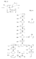
- Figure 4 is an exemplary flow chart of a procedure which may be implemented in the PWM module 12 based on the (modulated) e.g. SSCG clock signal from the generator 20 and the unmodulated signal from the generator 10 which may be used as "reference" with an unmodulated pulse repetition frequency of e.g. 20 KHz.
- modulated e.g. SSCG clock signal from the generator 20
- unmodulated signal from the generator 10 which may be used as "reference” with an unmodulated pulse repetition frequency of e.g. 20 KHz.
- T S T PWM_NOM
- T PWM_NOM the nominal value of the PWM period
- this may be maintained by using the clock signal from the generator 10 as a reference so that (by referring to the representation of Figure 3 ) T PWM_NOM and T PWM_MOD may coincide.
- C PWM_NOM e C PWM_MOD namely the count values of an internal counter to the module 12 which may dictate switching of the PWM signal (and thus the times T DC_NOM and T DC_MOD of Figure 3 , that is the duty cycle DC of the PWM signal) will generally differ from each other, with C PWM_NOM equal to T PWM_NOM * f 0 , where f 0 is the basic unmodulated frequency of the generator 20 (see Figure 2 ) while C PWM_MOD equals T PWM_NOM * f MOD , where f MOD is the actual current value of the modulated frequency of the generator 20 (see again Figure 2 ).
- the period of the PWM signal will be constant (with unmodulated duration) if expressed as a time value e.g. T PWM_NOM , and variable if expressed as a clock pulse/cycle count (C PWM_NOM or C PWM_MOD ).
- T PWM is used for brevity throughout Figures 5 to 8 in order to designate the PWM period which is controlled to correspond to the nominal value T PWM_NOM .
- a step 103 the value read for C N-1 is compared with a corresponding value C N-1_PRE previously predicted as better detailed in the following.
- C N-1 is found to be different from C N-1_PRE (possibly by taking into account a possible threshold
- the step-wise frequency modulation having a triangular modulation profile including upward and downward modulation steps may then be exploited for identifying a pair of values for the frequency of the frequency-modulated clock signal 20 out of plural (e.g. two) pairs as a function of the modulation profile (e.g. upward step or downward step) of the step-wise frequency modulation of the clock generator 20.
- a current pair of values for the frequency of the frequency-modulated clock signal of generator 20 may thus be identified as a function of a homologous previous pair of values for the frequency of the frequency-modulated clock signal of generator (20).
- values such as C D_N-1 and C D_N are indicative of the count values reached by the internal counter of the PWM module 12 when two subsequent frequency modulation steps, separated by a time interval T S , occur in two subsequent PWM cycles with a nominal period T PWM_NOM .
- a step 108 the value calculated for C D_N-1 is compared with a corresponding value C D_N-1_PRE previously predicted as better detailed in the following.
- C D_N-1 is found to be different from C D_N-1_PRE (possibly by taking into account a possible threshold
- ⁇ C THR' is threshold whose value may be dictated by the specific implementation considered and may possibly be zero
- C THR' is threshold whose value may be dictated by the specific implementation considered and may possibly be zero
- a check may be made in order to ascertain which of two conditions apply, namely:
- T D_N_PRE corresponds to C D_N_PRE , expressed as time, while C D_N PRE_RES , T D_N_PRE_RES are the residues in terms of clock cycles and time, which in this case are zero ( Figure 5a ).
- suffix _PRE indicates predicted values and the suffix _RES indicates residues, as defined previously, with C and T indicating entities expressed as clock cycles and times, respectively.
- C D_N_PRE 0
- C DUTY_F_W_N is the point, expressed as clock pulses/cycles at which a certain PWM control signal will go "low” (that is have a falling edge F) during a period N, while DC denotes the duty cycle as a percentage.
- index of the PWM signals W e
- index of the ADC signals K will generally refer to the windings W1, W2, W3 of the motor M and the associated ADC conversions.
- these may amount to two signals for each of the three windings so that W will generally take integer values from 0 to 5.
- T ADC denotes the instant in time at which a certain ADC conversion may be started.
- the same remarks made for the index W apply to the index K, save that the acquisition number may depend on the specific application considered.
- Figure 6 is an exemplary graphical representation of possible relationships among these parameters.
- C N_PRE f sys_mod_N_PRE * T PWM_NOM
- a check is made as to whether T DUTY_F_W_N ⁇ T D_N_PRE (where T DUTY_F_W_N DC N * T PWM_NOM ) .
- step 118 If the check yields a positive outcome, then the system evolves to a step 118. In the negative, the system evolves to a step 119.
- C DUTY_F_W_N C D_N_PRE + (T DUTY_F_W_N - T D_N_PRE ) * f sys_mod_x+1_N_PRE (which corresponds to the situation portrayed in Figure 7b ), with the same applying also to the ADC conversions (see Figure 8b ).
- the block 120 indicates an exit step after which the procedure just described may be repeated iteratively for a subsequent PWM period.
- One or more embodiments as exemplified herein thus relate to a method of controlling an electric motor M by means of at least one pulse-width modulated control signal (e.g. PWM, ADC - see Figure 1 ) having edge transitions occurring at one or more transition count values (e.g. C DUTY_F_W_N and C ADC_CONV_K_N ) of the pulses of the clock signal 20 which is frequency-modulated with a step-wise frequency modulation f mod (see e.g. Figure 2 ).
- the method may thus include:
- these predicted values may be predicted as a function of the frequency unmodulated clock signal 10, so that the transition count values (e.g. C DUTY_F_W_N and C ADC_CONV_K_N ) may be compensated against the step-wise frequency modulation of the clock signal 20.
- the transition count values e.g. C DUTY_F_W_N and C ADC_CONV_K_N
- the previous flow chart refers to the (non binding) assumption that T S ⁇ T PWM_NOM , that is that only one frequency modulation step may occur for each PWM period.
- T PWM_NOM > T S ⁇ T PWM_NOM /2 that is where one or two modulation step changes may occur for each PWM period.
- Steps 101 to 104 are unchanged.
- step 108 if C D1_N-1 is different from C D1_N-1_PRE or C D2_N-1 is different from C D2_N-1_PRE then the step 109 or the step 111 (modified as described in the following) may be performed.
- C D2_N-1 is always greater than zero so step 110 may be skipped.
- step 111 if 2*T PWM_NOM ⁇ T D2_N _N-1 + 2*T S then the step 112 (modified as described in the following) may be performed.
- steps 112 to 120 are performed as in the case of one modulation step change for each PWM period.
- the steps 117 to 119 can be easily generalized considering that in this case three cases are possible, namely: T DUTY_F_W_N ⁇ T D 1 _N_PRE , T D 1 _N_PRE ⁇ T DUTY_F_W_N ⁇ T D 2 _N_PRE and T D 2 _N_PRE ⁇ T DUTY_F_W_N , the same also applying to the ADC conversions.
- the procedure may be generalized by considering that if T PWM / 2 > T S ⁇ T PWM /4, three or two modulation step changes can occur for each PWM period and, in general, that if T PWM /k ⁇ T S ⁇ T PWM_ / k+1, (k+2) or (k+1) modulation step changes can occur for each PWM period.
- determining if one or more frequency modulation steps have occurred in the step-wise frequency modulation of the frequency-modulated clock signal 20 may involve easuring an average value for the frequency of the frequency-modulated clock signal 20 and comparing the average value measured with a set of values for the frequency of the frequency-modulated clock signal 20 in order to identify, as a function of the modulation profile of the step-wise frequency modulation, a pair of values for the frequency of the frequency-modulated clock signal leading to the average value measured.
- measuring an average value for the frequency of the frequency-modulated clock signal 20 may includes calculating a number of clock cycles of the frequency-modulated clock signal 20 occurring over at least a portion of the fixed period T PWM_NOM of the unmodulated clock signal 10, or retrieving the average value as a function of the difference between the numbers of clock cycles of the frequency-modulated clock signal 20 occurring over subsequent periods T PWM_NOM or over subsequent portions of the unmodulated clock signal 10.
- the PWM internal counter in the module 12 may be reset on each PWM pulse occurrence, by using the number of (modulated) clock cycles counted in processing as described.
- the PWM internal counter in the module 12 may not be reset on each PWM pulse occurrence, by using in processing as described the difference between the cumulative values stored at the end of the current PWM period N and the previous PWM period N-1.
- a value for f sys_mod_N may be retrieved in a look-up table (LUT) e.g. in the module 12 by using the difference between the current measured value for C N and a nominal value therefor as an entry to the table.
- LUT look-up table
- multiplications in the place of divisions, multiplications may be used as these latter may be faster to implement. For instance, multiplication by a frequency may be used in the place of division by a corresponding period.
Landscapes
- Engineering & Computer Science (AREA)
- Power Engineering (AREA)
- Physics & Mathematics (AREA)
- Electromagnetism (AREA)
- Control Of Electric Motors In General (AREA)
Abstract
Description
- The description relates to controlling electric motors.
- One or more embodiments may relate to electric motor control applications with a triangle wave modulated system clock.
- Electromagnetic interference (EMI), once the exclusive concern of equipment designers working with high speed signals, is no longer limited to a narrow class of high-end applications. Continued innovation in semiconductor technology has resulted in the ready availability of cost effective, high performance System-on-Chip (SoC) devices, MicroController Units (MCUs), processors, Digital Signal Processors (DSPs), Application Specific Integrated Circuits (ASICs), Field Programmable Gate Arrays (FPGAs) and Analog/Digital Converters (ADCs).
- High speed clocking signals used to control these ICs may however generate EMI and, as a consequence, more challenges for designers of consumer, enterprise, communications and embedded equipment.
- The need is therefore felt for improved arrangements adapted for use in such a challenging environment.
- An object of one or more embodiments is to satisfy such a need.
- According to one or more embodiments, that object is achieved thanks to a method as called for in the claims that follow.
- One or more embodiments may relate to a corresponding system and corresponding apparatus (e.g. an electric motor equipped with such a control system) as well as to a computer program product loadable the memory of at least one processing device (e.g. a PWM processor module for controlling an electric motor) and including software code portions for executing the steps of the method when the product is run on at least one computer. As used herein, reference to such a computer program product is understood as being equivalent to reference to a computer-readable means containing instructions for controlling the processing system in order to co-ordinate implementation of the method according to the invention. Reference to "at least one processor device" is intended to highlight the possibility for the present invention to be implemented in modular and/or distributed form.
- The claims are an integral part of the disclosure of one or more exemplary embodiments as provided herein.
- One or more embodiments may facilitate correcting the error introduced by a modulated clock for motor control applications when using a modulated clock for the overall system.
- One or more embodiments may permit to avoid, or at least reduce, the use of other conventional EMI-lowering techniques such as e.g. filtering, shielding, good layout practice with advantages in terms of cost and time.
- One or more embodiments will now be described, by way of example only, with reference to the annexed figures, in which:
-
Figure 1 is a schematic representation of a control system for an electric motor; -
Figure 2 exemplifies a modulation signal for use in one or more embodiments; -
Figure 3 is exemplary of possible effects of a modulated system clock on PWM control signals; -
Figure 4 is an exemplary flow-chart of operation of one or more embodiments; and -
Figures 5 to 8 are time diagrams in support of the description of the exemplary flow chart ofFigure 4 . - In the ensuing description one or more specific details are illustrated, aimed at providing an in-depth understanding of examples of embodiments. The embodiments may be obtained without one or more of the specific details, or with other methods, components, materials, etc. In other cases, known structures, materials, or operations are not illustrated or described in detail so that certain aspects of embodiments will not be obscured.
- Reference to "an embodiment" or "one embodiment" in the framework of the present description is intended to indicate that a particular configuration, structure, or characteristic described in relation to the embodiment is comprised in at least one embodiment. Hence, phrases such as "in an embodiment" or "in one embodiment" that may be present in one or more points of the present description do not necessarily refer to one and the same embodiment. Moreover, particular conformations, structures, or characteristics may be combined in any adequate way in one or more embodiments.
- The references used herein are provided merely for convenience and hence do not define the extent of protection or the scope of the embodiments.
- In various applications, an effective and efficient approach to controlling and reducing ElectroMagnetic Interference (EMI) may involve Spread Spectrum Clock Generation (SSCG) technology: instead of maintaining a constant frequency, spread spectrum techniques modulate a system clock across a (much) smaller frequency range that creates a frequency spectrum with sideband harmonics. By intentionally spreading the narrowband repetitive clock across a broader band, the peak spectral energy of both the fundamental and harmonic frequencies can be reduced simultaneously. Effectively, an SSCG clock IC adds controlled jitter by increasing and decreasing the clock frequency e.g. linearly. While the total radiated energy in the signal is the same as in the case of an unmodulated signal, the spectral components occur at a lower magnitude due to spreading across more frequencies/greater bandwidth. End developers my thus are able to reduce EMI to desired levels.
- Spread spectrum clock generation may result in an effective reduction of EMI throughout the system compared to other EMI reduction methods. Specifically, since the clock and timing signals derived from an SSCG clock are modulated by the same percentage (including e.g. buses and interconnects), EMI reduction from SSCG technology benefits the entire system, not just a local circuit.
- For various applications, implementing a spread spectrum clock into a system e.g. during the early design stages can mitigate appreciably the need for further EMI reduction measures. For instance, a triangular modulation wave may be used with programmable modulation frequency (fmod) and modulation depth percentage (MD).
- The error introduced by the modulated clock may not be acceptable for certain applications, and an additional non-modulated clock might be used in those parts of the system where a stable non-modulated clock is required.
- This may apply, e.g. to electric motor control applications, e.g. PWM (Pulse Width Modulation) control of an electric motor M where (in a manner known per se, which makes it unnecessary to provide a more detailed description herein) PWM signals are generated for feeding to the motor windings (see e.g. W1, W2, W3 in
Figure 1 ) along with trigger signals sent to analog-to-digital converters (ADCs) 14 for sampling the motor phase currents and/or other signals used for the control. - As result, the EMI reduction effect may not extend to the whole system and other traditional EMI-lowering techniques such as filtering, shielding, and good layout practice are implemented, which add to the cost and the time involved in the design of the system.
- One or more embodiments as exemplified in
Figure 1 may include afirst clock generator 10 adapted to generate a non-modulated (unmodulated) clock signal, that is a non-modulated clock signal including a train of pulses with a fixed period. In one or more embodiments, this may be a low-frequency, e.g. 20 KHz, signal with a period selected to be equal to a nominal value TPWM_NOM of the PWM period, e.g. 50 microseconds. - In one or more embodiments, the duration of the pulses may be reduced to a (minimum) value sufficient to permit detection by a
PWM modulator sub-module 12 in order to generate (in a manner known per se, which is not a subject-matter of the embodiments) PWM-modulated control signals for an electric motor M. - These control signals may include, e.g.:
- PWM drive signals for feeding to the motor windings W1, W2, W3,
- trigger signals ADC for the analog-to-digital converters 14 for sampling the motor phase currents and/or any other signals used for the controlling the motor M. For instance, in one or more embodiments, the signals ADC may mark the conversion start times for the analog-to-digital converters.
- The designation "control signal" will be used herein for the sake of simplicity to designate collectively signals such as the PWM drive signals and the ADC trigger signals in
Figure 1 . - In one or more embodiments, the clock signal (pulse train) from the
generator 10 may be used for determining a desired - constant - period of the PWM signal in themodule 12. For instance, in one or more embodiments, the clock signal from thegenerator 10 may positively reset (or "capture") a PWM counter in themodule 12. - One or more embodiments may be resort to such an approach in view of the fact that generation of the control signals via such a counter in the
module 12 may take place as a function of the clock pulses provided by a frequency-modulated by a e.g. triangle wave (modulating) signal of asecond generator 20. -
Figure 2 is an exemplary representation of such a e.g. center spread (step-wise) triangle wave modulation with programmable modulation frequency fmod around a base frequency fo and modulation depth percentage MD, where the number of modulation steps is fixed. - The second generator 20 (e.g. a FMPLL) is exemplary of a system clock signal generated in compliance with Spread Spectrum Clock Generation (SSCG) technology in order to counter EMI effects as discussed in the introductory portion of this description. It will be appreciated that, while the diagram of
Figure 2 depicts per se the amplitude of the modulation signal over time (abscissa scale), the ordinate values are plotted against a resulting modulation frequency. - By referring, again purely by way of example, to the exemplary numerical values indicated in the foregoing (e.g. an unmodulated 20 KHz clock from the generator 10), the triangular-wave modulation signal from the circuit 20 (e.g. a FMPLL) may correspond to a SSCG modulation in a frequency range between 142.68 MHz and 150 MHz, with a quantized modulation amplitude of e.g. 4.88%. The modulation change may take place in
S steps - Frequency changes may occur e.g. at instants separated by a time TS. For the sake of simplicity TS-that is the time between two modulation steps - will be assumed to be constant.
- Also, operation of one or more embodiments will be first exemplified under the assumption that TS ≥ TPWM_NOM, where TPWM_NOM is the nominal value of period of the PWM control signals, so that only one modulation step may be assumed to occur during one PWM period.
- Consistently, the left-hand side of
Figure 2 exemplifies an (upward) modulation step taking place during a PWM period N-1 from a frequency fsys_mod_x'_N-1 to a frequency fsys_mod_x'+1_N-1 resulting in an average value fsys_mod_n-1 for the frequency of theclock generator 20 over the period N-1. - An identical average value may result from e.g. a (downward) modulation step from a frequency fsys_mod_x"_N-1 and a frequency fsys_mod_x"+1_N-1.
- Whatever the numerical values selected and the specific criteria adopted for producing the PWM control signals (e.g. for modulating their pulse width) generation by conventional means as a function of a frequency-modulated clock signal as generated by the
generator 20 and including rising and fallingfrequency modulation steps - This situation is exemplified in the diagram of
Figure 3 . There the "nominal" expected values of the period and the "on" period (which dictates the duty cycle) of the PWM control signals are denoted by TPWM_NOM and TDC_NOM, respectively. - A frequency change in the clock signal from the
generator 20 might result in a change of both these PWM control signals to actual "modulated" values TPWM_MOD and TDC_MOD. - This may be understood by noting that an internal counter within the
PWM module 12, when clocked with the modulated signal from thegenerator 20, may reach any count values set to switch the PWM signal (e.g. from "0" to "1" or from "1" to "0") either "earlier" or "later", depending on whether he frequency of the modulated signal from thegenerator 20 is subjected to an upward or downward modulation step as exemplified inFigure 2 . -
Figure 3 exemplifies a case where, following a change of frequency CF, TPWM_MOD < TPWM_NOM and TDC_MOD < TDC_NOM. More generally, a frequency modulation step in the modulated signal from thegenerator 20 may result in TDC_NOM/TPWM_NOM ≠ TDC_MOD/TPWM_MOD. - This may be adversely affect operation of the motor M both because the motor windings W1, W2, W3 may be supplied with PWM drive signals having a time behaviour different from the nominal expected behaviour, and because the analog-to-digital converters for sampling the motor phase currents and/or any other signals used for the controlling the motor may be triggered at "incorrect" times.
- Just by way of reference, a PWM control signal with a period having a nominal duration TPWM_NOM of 50 microseconds (20kHz) corresponding to 7500 cycles of an unmodulated 150 MHz system clock would have its duration varied in the range between 50 and 52.57 microseconds with a system clock subjected to modulation in a frequency range between 142.68 MHz and 150 MHz.
-
Figure 4 is an exemplary flow chart of a procedure which may be implemented in thePWM module 12 based on the (modulated) e.g. SSCG clock signal from thegenerator 20 and the unmodulated signal from thegenerator 10 which may be used as "reference" with an unmodulated pulse repetition frequency of e.g. 20 KHz. - For the sake of simplicity, an exemplary procedure will first be described under the assumption - already considered in the foregoing - of a single frequency modulation step during a PWM period, that is TS ≥ TPWM_NOM where TPWM_NOM is the nominal value of the PWM period; in one or more embodiments, this may be maintained by using the clock signal from the
generator 10 as a reference so that (by referring to the representation ofFigure 3 ) TPWM_NOM and TPWM_MOD may coincide. - It will be otherwise be noted that CPWM_NOM e CPWM_MOD, namely the count values of an internal counter to the
module 12 which may dictate switching of the PWM signal (and thus the times TDC_NOM and TDC_MOD ofFigure 3 , that is the duty cycle DC of the PWM signal) will generally differ from each other, with CPWM_NOM equal to TPWM_NOM * f0, where f0 is the basic unmodulated frequency of the generator 20 (seeFigure 2 ) while CPWM_MOD equals TPWM_NOM * fMOD, where fMOD is the actual current value of the modulated frequency of the generator 20 (see againFigure 2 ). - In this exemplary description, T is used to indicate values expressed as times (e.g. TPWM_NOM = TPWM_MOD, TS being the time between two modulation steps, and so on), while C denotes in general expressed as clock pulses (clock cycles) or counts (e.g. CPWM_NOM ≠ CPWM_MOD) . As a result, the period of the PWM signal will be constant (with unmodulated duration) if expressed as a time value e.g. TPWM_NOM, and variable if expressed as a clock pulse/cycle count (CPWM_NOM or CPWM_MOD). For that reason, the designation TPWM is used for brevity throughout
Figures 5 to 8 in order to designate the PWM period which is controlled to correspond to the nominal value TPWM_NOM. - In a
step 101, a number CN-1 of the (modulated) clock pulses/cycles from thegenerator 20 during a PWM period N-1 will be read and in a step 102 a value fsys_mod_n-1 for the average frequency of theclock generator 20 over the period N-1 will be calculated as:
generator 10, used as a reference. - In a
step 103 the value read for CN-1 is compared with a corresponding value CN-1_PRE previously predicted as better detailed in the following. - If CN-1 is found to be different from CN-1_PRE (possibly by taking into account a possible threshold | CN-1 - CN-1_PRE | < CTHR, where CTHR is a threshold with value - e.g. 1 or 2 pulses - which is dictated by the specific implementation considered and may possibly be zero) then the system exits to a
reaction step 104 which is application dependent, e.g. a safe reset state. - Else, in a
step 105, the value calculated for fsys_mod_n-1 may be compared with fsys_mod_y_N-1 (with y = 0, 1, ..., S-1), that is with the possible (modulated) values for the frequency of theclock generator 20 in order to identify, by considering the modulation profile, a pair of values out of fsys_mod_x'_N-1, fsys_mod_x'+1_N-1 and fsys_mod_x"_N-1, fsys_mod_x''+1_N-1 which may lead to an average value fsys_mod_N-1 depending on whether the condition fsys_mod_x'_N-1 ≤ fsys_mod_N-1 ≤ fsys_mod_x'+1_N-1 (upward modulation: seeFigure 2 ) or the condition fsys_mod_x''_N-1 ≥ fsys_mod_N-1 ≥ fsys_mod_x''+1_N-1 (downward modulation: see againFigure 2 ) applies. - In one or more embodiments the step-wise frequency modulation having a triangular modulation profile including upward and downward modulation steps (see
Figure 2 ) may then be exploited for identifying a pair of values for the frequency of the frequency-modulatedclock signal 20 out of plural (e.g. two) pairs as a function of the modulation profile (e.g. upward step or downward step) of the step-wise frequency modulation of theclock generator 20. - In a step 106 a pair fsys_mod_x_N-1, fsys_mod_x+1_N-1 is selected:


- In a step 107 a value CD_N-1 = CN-1 * (fsys_mod_N-1-fsys_mod_x+1_N-1) / (fsys_mod_x_N-1 - fsys_mod_x+1_N-1) and TD_N-1 = CD_N-1/fsys_mod_x_N-1 is calculated
- The possible presence of the term fsys_mod_x+1_N-2 indicates that the first term in the current period term may coincide with the second term in the pair for the previous period: such a condition may thus be exploited for identifying the pair for the current period once the pair for the previous period is known. A current pair of values for the frequency of the frequency-modulated clock signal of
generator 20 may thus be identified as a function of a homologous previous pair of values for the frequency of the frequency-modulated clock signal of generator (20). - As schematically represented in
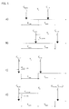
Figure 5 a) , values such as CD_N-1 and CD_N are indicative of the count values reached by the internal counter of thePWM module 12 when two subsequent frequency modulation steps, separated by a time interval TS, occur in two subsequent PWM cycles with a nominal period TPWM_NOM. - In a
step 108 the value calculated for CD_N-1 is compared with a corresponding value CD_N-1_PRE previously predicted as better detailed in the following. - If CD_N-1 is found to be different from CD_N-1_PRE (possibly by taking into account a possible threshold | CD_N-1 - CD_N-1_PRE | < CTHR', where CTHR' is threshold whose value may be dictated by the specific implementation considered and may possibly be zero) then the system exits to a
reaction step 109 which is application dependent, e.g. a safe reset state. - Else, in a step 110:

- The case CD_N-1 = 0 corresponds to no frequency changes occurring during the current period N-1 (see
-
Figure 5c ), so that during the subsequent period N a residue in time (and clock cycles) for the period N-2 may be taken into account by subtracting them from the time TS. - One or more embodiments may thus involve:
- detecting if a frequency modulation step in the step-wise frequency modulation of the clock signal of
generator 20 has occurred over a certain time TS, and - if no such frequency modulation step has occurred (that is, CD_N-1 = 0) a time or count residue may be applied to at a subsequent detection time TS, preferably by subtracting that residue from said subsequent detection time.
- Such a residue is indicated in the following by the suffix _RES. By modifying correspondingly CD_N-1 e TD_N-1, the formula of the
step 112 will apply also to the case where CD_N-1 is zero. Referring to these residues makes it simpler to indicate in the figures the meaning of (CN-2 - CD_N-2) and (TPWM_NOM - TD_N-2). - In a step 111 a check may be made in order to ascertain which of two conditions apply, namely:
- if 2*TPWM_NOM ≥ TD_N-1 = + TS, then the system evolves to a
step 112; - if TD_N-1 = + TS ≥ 2*TPWM_NOM then the system evolves to a
step 113. - Various conditions possibly underlying the
steps 110 to 114 are portrayed inFigure 5 . -
Figure 5a ) portrays the case where 2*TPWM_NOM ≥ TD_N-1 + TS with TD_N-1 = > 0, where TD_N-1 = corresponds to CD_N-1 expressed as a time. -
Figure 5b ) portrays the case where TD_N-1 = + TS ≥ 2*TPWM_NOM, again with TD_N-1 = > 0. -
Figures 5c) and 5d ) portray the cases where: - CD_N-1 = 0 and CD_N-1_RES > 0;
- CD_N-1 = 0 and CD_N = 0.
- In the
step 112, a prediction of CD_N is made based on TD_N_PRE = TS + TD_N-1 = TPWM_NOM and with CD_N_PRE_RES = TD_N_PRE_RES = 0 (seeFigure 5a ) - Again TD_N_PRE corresponds to CD_N_PRE, expressed as time, while CD_N PRE_RES, TD_N_PRE_RES are the residues in terms of clock cycles and time, which in this case are zero (
Figure 5a ). - In the case CD_N-1 = 0, the system is updated according to the condition CD_N-1 = - CD_N-1_RES so that TD_N_PRE = Ts - TD_N-1_RES - TPWM_(see
Figure 5c , which corresponds to the condition where CD_N-1 - 0 and CD_N-1_RES> 0) is correctly predicted. - Alternatively, in the
step 113, a prediction of CD_N is made based on CD_N_PRE = 0 and TD_N_PRE_RES = TPWM_NOM - TD_N-1 (seeFigure 5b ), where CD_N_PRE_RES is the residue (in terms of clock cycles), which differs from zero (only) if CD_N_PRE is equal to a zero. - In the
step 114, if CD_N_PRE = 0, then fsys_mod_N_PRE = fsys_mod_x_N_PRE = fsys_mod_x+1_N_PRE = fsys_mod_x+1_N-1, that is no modulation step change has occurred during the period N; CN_PRE = TPWM_NOM * fsys_mod_x_N_PRE and CD_N_PRE_RES = CN_PRE CD_N-1 - In case of CD_N-1 = 0 and CD_N = 0, CD_N-1 = - CD_N-1_RES so TD_N_PRE_RES = TPWM_NOM + TD_N-1_RES and in the next period the value can be correctly predicted as TD_N+1_PRE = TS + TD_N - TPWM_NOM = TS - TD_N_PRE_RES - TPWM_NOM = TS - (TPWM_NOM + TD_N-1_RES) - TPWM_NOM = TS - TD_N-1_RES - 2*TPWM_NOM (see
Figure 5d ) - Again, the suffix _PRE indicates predicted values and the suffix _RES indicates residues, as defined previously, with C and T indicating entities expressed as clock cycles and times, respectively.
- In a step 115 (CD_N_PRE = 0) - with a concept which may be easily generalized in case of center-aligned PWM - values CDUTY_F_W_N (corresponding to TDUTY_F_W_N) equal to DCW_N * CN_PRE and CADC_CONV_K_N = TADC_CONV_K_N * fsys_mod_N_PRE may be calculated where DC is the duty cycle in percentage to be set, W is the index of the PWM signals and K is the index of the ADC conversions.
- Here, the suffix F is used to designate the falling edge in the PWM duty cycle: for instance CDUTY_F_W_N is the point, expressed as clock pulses/cycles at which a certain PWM control signal will go "low" (that is have a falling edge F) during a period N, while DC denotes the duty cycle as a percentage.
- The designations "index of the PWM signals W" e "index of the ADC signals K" will generally refer to the windings W1, W2, W3 of the motor M and the associated ADC conversions.
- In one or more embodiments, these may amount to two signals for each of the three windings so that W will generally take integer values from 0 to 5.
- TADC denotes the instant in time at which a certain ADC conversion may be started. The same remarks made for the index W apply to the index K, save that the acquisition number may depend on the specific application considered.
-
Figure 6 is an exemplary graphical representation of possible relationships among these parameters. - In a step 116 (CD_N_PRE > 0) a number of entities are defined/calculated, namely:


- In a step 117 (CD_N_PRE > 0) a check is made as to whether TDUTY_F_W_N < TD_N_PRE (where TDUTY_F_W_N = DCN * TPWM_NOM) .
- If the check yields a positive outcome, then the system evolves to a
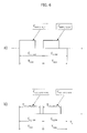
step 118. In the negative, the system evolves to astep 119. - In the step 118 CDUTY_F_W_N = (TDUTY_F_W_N / TD_N_PRE) * CD_N_PRE (which corresponds to the situation portrayed in
Figure 7a ), with the same applying also to the ADC conversions (seeFigure 8a ). - In the step 119 CDUTY_F_W_N = CD_N_PRE + (TDUTY_F_W_N - TD_N_PRE) * fsys_mod_x+1_N_PRE (which corresponds to the situation portrayed in
Figure 7b ), with the same applying also to the ADC conversions (seeFigure 8b ). - The
block 120 indicates an exit step after which the procedure just described may be repeated iteratively for a subsequent PWM period. - One or more embodiments as exemplified herein thus relate to a method of controlling an electric motor M by means of at least one pulse-width modulated control signal (e.g. PWM, ADC - see
Figure 1 ) having edge transitions occurring at one or more transition count values (e.g. CDUTY_F_W_N and CADC_CONV_K_N) of the pulses of theclock signal 20 which is frequency-modulated with a step-wise frequency modulation fmod (see e.g.Figure 2 ). In one or more embodiments the method may thus include: - providing a frequency
unmodulated clock signal 10 having a fixed pulse period TPWM_NOM indicative of the period of the pulse-width modulated control signals PWM, ADC; and - setting the count values CDUTY_F_W_N and CADC_CONV_K_N as a function of e.g. predicted count value CN_PRE and a predicted frequency value fsys_mod_N_PRE for the frequency-modulated
clock signal 20. - In one or more embodiments these predicted values may be predicted as a function of the frequency
unmodulated clock signal 10, so that the transition count values (e.g. CDUTY_F_W_N and CADC_CONV_K_N) may be compensated against the step-wise frequency modulation of theclock signal 20. - As indicated, the previous flow chart refers to the (non binding) assumption that TS ≥ TPWM_NOM, that is that only one frequency modulation step may occur for each PWM period.
- The procedure exemplified in the foregoing may be extended to the case where e.g. TPWM_NOM > TS ≥ TPWM_NOM /2, that is where one or two modulation step changes may occur for each PWM period.
- In that case, the flow chart of
Figure 4 may be modified as detailed in the following. -
Steps 101 to 104 are unchanged. - In
step 105, fsys_mod_N-1 is compared with fsys_mod_y'_N-1 (with y = 0, 1, ..., S-1) where fsys_mod_y'_N-1 is defined as fsys_mod_y'_N-1 = (fsys_mod_y_N-1 + fsys_mod_y+1_N-1) /2 in order to identify the frequency fsys_mod_x'_N-1 of the triad (fsys_mod_x'-1_N-1, fsys_mod_x'_N-1, fsys_mod_x'+1_N-1) and the frequency fsys_mod_x"_N-1 of the triad (fsys_mod_x"-1_N-1, fsys_mod_x''_N-1, fsys_mod_x''+1_N-1). - In
step 106, if fsys_mod_x'_N-1 = fsys_mod_x+1_N-2 or fsys_mod_x"_N-1 = fsys_mod_x+1_N-2 then thesteps 106 to 109 (or 110) are performed as in the case of a single modulation step change during a PWM period. - Else, if fsys_mod_x'-1_N-1 = fsys_mod_x+1_N-2 then (fsys_mod_x-1_N-1, fsys_mod_x_N-1, fsys_mod_x+1_N-1) = (fsys_mod_x'-1_N-1, fsys_mod_x'_N-1 , fsys_mod_x'+1_N-1) else (fsys_mod_x-1_N-1,
f sys_mod_x_N-1, fsys_mod_x+1_N-1) = (fsys_mod_x'-1_N-1, fsys_mod_x'_N-1, fsys_mod_x'+1_N-1). - In
step 107, by considering fsys_mod_N-1 = (fsys_mod_x-1_N-1 * TD1_N + fsys_mod_x_N-1 * (TD2_N - TD1_N) + fsys_mod_x+1_N-1 * (TPWM - TD2_N) / TPWM_with TD2_N = TS + TD1_N, TD1_N and TD2_N can be calculated and so CD1_N-1 = TD1_N-1 * fsys_mod_x-1_N-1 and CD2_N-1 = TS * fsys_mod_x_N-1. - In
step 108, if CD1_N-1 is different from CD1_N-1_PRE or CD2_N-1 is different from CD2_N-1_PRE then thestep 109 or the step 111 (modified as described in the following) may be performed. - In that respect it will be observed that CD2_N-1 is always greater than zero so step 110 may be skipped.
- In
step 111, if 2*TPWM_NOM ≥ TD2_N _N-1 + 2*TS then the step 112 (modified as described in the following) may be performed. - Else the
steps 112 to 120 are performed as in the case of one modulation step change for each PWM period. - In the
step 112, TD1_N_PRE = Ts + TD2_N-1 - TPWM and TD2_N N_PRE = TS + TD1_N_PRE and in thestep 116 the following calculations are performed:



- The
steps 117 to 119 can be easily generalized considering that in this case three cases are possible, namely:


- Those of skilled in the art will otherwise appreciated that the procedure may be generalized by considering that if TPWM/ 2 > TS ≥ TPWM/4, three or two modulation step changes can occur for each PWM period and, in general, that if TPWM/k ≥ TS ≥ TPWM_/
k+ 1, (k+2) or (k+1) modulation step changes can occur for each PWM period. - Here again, as throughout the embodiments exemplified herein, determining if one or more frequency modulation steps have occurred in the step-wise frequency modulation of the frequency-modulated
clock signal 20 may involve easuring an average value for the frequency of the frequency-modulatedclock signal 20 and comparing the average value measured with a set of values for the frequency of the frequency-modulatedclock signal 20 in order to identify, as a function of the modulation profile of the step-wise frequency modulation, a pair of values for the frequency of the frequency-modulated clock signal leading to the average value measured. - Also, throughout the embodiments exemplified herein, measuring an average value for the frequency of the frequency-modulated
clock signal 20 may includes calculating a number of clock cycles of the frequency-modulatedclock signal 20 occurring over at least a portion of the fixed period TPWM_NOM of theunmodulated clock signal 10, or retrieving the average value as a function of the difference between the numbers of clock cycles of the frequency-modulatedclock signal 20 occurring over subsequent periods TPWM_NOM or over subsequent portions of theunmodulated clock signal 10. - Whatever the specific procedure adopted, all the related processing may be conveniently performed e.g. at a firmware level in the
PWM submodule 12. - In one or more embodiments, the PWM internal counter in the
module 12 may be reset on each PWM pulse occurrence, by using the number of (modulated) clock cycles counted in processing as described. - In one or more embodiments, the PWM internal counter in the
module 12 may not be reset on each PWM pulse occurrence, by using in processing as described the difference between the cumulative values stored at the end of the current PWM period N and the previous PWM period N-1. - In one or more embodiments, as an alternative to calculation as described in the foregoing, a value for fsys_mod_N may be retrieved in a look-up table (LUT) e.g. in the
module 12 by using the difference between the current measured value for CN and a nominal value therefor as an entry to the table. - In one or more embodiments, in the place of divisions, multiplications may be used as these latter may be faster to implement. For instance, multiplication by a frequency may be used in the place of division by a corresponding period.
- Without prejudice to the underlying principles, the details and embodiments may vary, even significantly, with respect to what has been described by way of example only, without departing from the extent of protection.
- The extent of protection is defined by the annexed claims.
Claims (10)
- A method of controlling an electric motor (M) by means of at least one pulse-width modulated control signal (PWM, ADC) having edge transitions occurring for at least one transition count value (CDUTY_F_W_N, CADC_CONV_K_N) of the pulses of a clock signal (20) which is frequency-modulated with a step-wise frequency modulation (fmod), the method including:- providing a frequency unmodulated clock signal (10) having a fixed period (TPWM_NOM) indicative of the period of said at least one pulse-width modulated control signal (PWM, ADC); and- setting said at least one transition count value (CDUTY_F_W_N, CADC_CONV_K_N) as a function of at least one of a predicted count value (CN_PRE) and a predicted frequency value (fsys_mod_N_PRE) for said frequency-modulated clock signal (20) predicted as a function of said frequency unmodulated clock signal (10), whereby said at least one transition count value (CDUTY_F_W_N, CADC_CONV_K_N) is compensated against said step-wise frequency modulation.
- The method of claim 1, wherein predicting said predicted frequency value (fsys_mod_N_PRE) for said frequency-modulated clock signal (20) includes measuring an average value (fsys_mod_N-1) for the frequency of said frequency-modulated clock signal (20) and comparing said average value measured (fsys_mod_N-1) with a set of values for the frequency of said frequency-modulated clock signal (20) in order to identify a pair of values for the frequency of said frequency-modulated clock signal (20) leading to said average value (fsys_mod_N-1) measured, thus determining if at least one frequency modulation step has occurred in said step-wise frequency modulation (fmod) of said frequency-modulated clock signal (20).
- The method of claim 2, wherein said step-wise frequency modulation (fmod) has a, preferably triangular, modulation profile including upward and downward modulation steps, the method including identifying said pair of values for the frequency of said frequency-modulated clock signal (20) out of plural pairs as a function of the modulation profile of said step-wise frequency modulation.
- The method of claim 2 or claim 3, including identifying a current pair of values for the frequency of said frequency-modulated clock signal (20) as a function of a homologous previous pair of values for the frequency of said frequency-modulated clock signal (20).
- The method of any of claim 2 to 4, including generating said average value (fsys_mod_N-1) for the frequency of said frequency-modulated clock signal (20) as a function of:- i) a number of clock cycles of said frequency-modulated clock signal (20) occurring over at least a portion of the fixed period (TPWM_NOM) of said unmodulated clock signal (10), or- ii) difference between the numbers of clock cycles of said frequency-modulated clock signal (20) occurring over subsequent periods (TPWM_NOM) or over subsequent portions of said unmodulated clock signal (10).
- The method of any of the previous claims, including:- detecting if a frequency modulation step in said step-wise frequency modulation (fmod) has occurred over a certain time (TS), and- if no frequency modulation step in said step-wise frequency modulation (fmod) has occurred over said certain time (TS), applying a time or count residue to a subsequent detection time (TS), preferably by subtracting said residue from said subsequent detection time.
- The method of any of the previous claims, wherein:- said frequency-modulated clock signal is a high-frequency clock signal to which spread spectrum clock generation is applied, preferably with a triangular step-wise frequency modulation (fmod), and- said frequency unmodulated clock signal (10) is a low frequency clock signal, with said fixed period (TPWM_NOM) preferably equal to the period of said at least one pulse-width modulated control signal (PWM, ADC).
- A control system for controlling an electric motor (M), including:- a frequency modulated clock generator (20) for generating a clock signal (20) which is frequency-modulated with a step-wise frequency modulation (fmod) ;- a pulse width modulation module (12) for generating at least one pulse-width modulated control signal (PWM, ADC) for said motor (M), said at least one pulse-width modulated control signal (PWM, ADC) having edge transitions occurring for at least one transition count value (CDUTY_F_W_N, CADC_CONV_K_N) of the pulses of a clock signal (20) which is frequency-modulated with a step-wise frequency modulation (fmod) ;- a frequency unmodulated clock generator (10) for generating a frequency unmodulated clock signal (10) having a fixed period (TPWM_NOM) indicative of the period of said at least one pulse-width modulated control signal (PWM, ADC);wherein said pulse width modulation module (12) is configured for setting said at least one transition count value (CDUTY_F_W_N, CADC_CONV_K_N) as a function of at least one of a predicted count value (CN_PRE) and a predicted frequency value (fsys_mod_N_PRE) for said frequency-modulated clock signal (20) predicted as a function of said frequency unmodulated clock signal (10) according to the method of any of claims 1 to 7, whereby said at least one transition count value (CDUTY_F_W_N, CADC_CONV_K_N) is compensated against said step-wise frequency modulation.
- An electric motor (M) equipped with a control system according to claim 8.
- A computer program product loadable the memory of at least one processor module (12) and including software code portions for executing the steps of the method of any of claims 1 to 7 when the product is run on at least one processor module.
Applications Claiming Priority (1)
| Application Number | Priority Date | Filing Date | Title |
|---|---|---|---|
| ITUB2015A002345A ITUB20152345A1 (en) | 2015-07-21 | 2015-07-21 | PROCEDURE FOR CHECKING ELECTRIC MOTORS, SYSTEM, ELECTRIC MOTOR AND CORRESPONDENT IT PRODUCT |
Publications (2)
| Publication Number | Publication Date |
|---|---|
| EP3121955A1 true EP3121955A1 (en) | 2017-01-25 |
| EP3121955B1 EP3121955B1 (en) | 2021-03-17 |
Family
ID=54289010
Family Applications (1)
| Application Number | Title | Priority Date | Filing Date |
|---|---|---|---|
| EP16161467.2A Active EP3121955B1 (en) | 2015-07-21 | 2016-03-21 | A method of controlling electric motors, corresponding system, electric motor and computer program product |
Country Status (3)
| Country | Link |
|---|---|
| US (1) | US10468948B2 (en) |
| EP (1) | EP3121955B1 (en) |
| IT (1) | ITUB20152345A1 (en) |
Families Citing this family (5)
| Publication number | Priority date | Publication date | Assignee | Title |
|---|---|---|---|---|
| US11349523B2 (en) * | 2017-08-10 | 2022-05-31 | Intel Corporation | Spread-spectrum modulated clock signal |
| WO2019089756A1 (en) * | 2017-11-06 | 2019-05-09 | Gojo Industries, Inc. | Touch-free dispensers |
| US12301148B2 (en) | 2020-10-21 | 2025-05-13 | Hitachi Astemo, Ltd. | Motor control device, electro-mechanical integrated unit, hybrid system, and electric power steering system |
| CN112994445B (en) * | 2021-04-25 | 2021-07-27 | 四川蕊源集成电路科技有限公司 | Apparatus and method for reducing electromagnetic interference of DC-DC power supply |
| CN114329973A (en) * | 2021-12-29 | 2022-04-12 | 深圳市朗科智能电气股份有限公司 | Method for reducing electromagnetic conducted interference of brushless motor control system |
Citations (2)
| Publication number | Priority date | Publication date | Assignee | Title |
|---|---|---|---|---|
| JP4361476B2 (en) * | 2004-12-22 | 2009-11-11 | 株式会社リコー | Image reading apparatus and image forming apparatus |
| US20100090775A1 (en) * | 2008-10-09 | 2010-04-15 | Muzahid Bin Huda | Method and Apparatus for Dynamic Modulation |
Family Cites Families (3)
| Publication number | Priority date | Publication date | Assignee | Title |
|---|---|---|---|---|
| JP4390646B2 (en) * | 2004-07-09 | 2009-12-24 | Necエレクトロニクス株式会社 | Spread spectrum clock generator and modulation method thereof |
| JP5165463B2 (en) * | 2008-05-28 | 2013-03-21 | ルネサスエレクトロニクス株式会社 | PWM control apparatus and pulse waveform control method |
| TWI551053B (en) * | 2015-01-14 | 2016-09-21 | 新唐科技股份有限公司 | Pulcse width modulation signal generation circuit and method |
-
2015
- 2015-07-21 IT ITUB2015A002345A patent/ITUB20152345A1/en unknown
-
2016
- 2016-03-10 US US15/066,802 patent/US10468948B2/en active Active
- 2016-03-21 EP EP16161467.2A patent/EP3121955B1/en active Active
Patent Citations (2)
| Publication number | Priority date | Publication date | Assignee | Title |
|---|---|---|---|---|
| JP4361476B2 (en) * | 2004-12-22 | 2009-11-11 | 株式会社リコー | Image reading apparatus and image forming apparatus |
| US20100090775A1 (en) * | 2008-10-09 | 2010-04-15 | Muzahid Bin Huda | Method and Apparatus for Dynamic Modulation |
Non-Patent Citations (2)
| Title |
|---|
| BALCELLS J ET AL: "EMI Reduction in Switched Power Converters Using Frequency Modulation Techniques", IEEE TRANSACTIONS ON ELECTROMAGNETIC COMPATIBILITY, IEEE SERVICE CENTER, NEW YORK, NY, US, vol. 47, no. 3, 1 August 2005 (2005-08-01), pages 569 - 576, XP011140192, ISSN: 0018-9375, DOI: 10.1109/TEMC.2005.851733 * |
| SANTOLARIA A ET AL: "Evaluation of switching frequency modulation in EMI emissions reduction applied to power converters", THE 29TH ANNUAL CONFERENCE OF THE IEEE INDUSTRIAL ELECTRONICS SOCIETY, 2003. IECON '03, IEEE SERVICE CENTER, PISCATAWAY, NJ, vol. 3, 2 November 2003 (2003-11-02), pages 2306 - 2311, XP010691430, ISBN: 978-0-7803-7906-0, DOI: 10.1109/IECON.2003.1280604 * |
Also Published As
| Publication number | Publication date |
|---|---|
| US20170025929A1 (en) | 2017-01-26 |
| EP3121955B1 (en) | 2021-03-17 |
| ITUB20152345A1 (en) | 2017-01-21 |
| US10468948B2 (en) | 2019-11-05 |
Similar Documents
| Publication | Publication Date | Title |
|---|---|---|
| EP3121955B1 (en) | A method of controlling electric motors, corresponding system, electric motor and computer program product | |
| EP2561605B1 (en) | A power supply and method of operation | |
| US10530252B2 (en) | Pulse-frequency control circuit, microcomputer, DC-to-DC converter, and pulse-frequency control method | |
| US20100090775A1 (en) | Method and Apparatus for Dynamic Modulation | |
| KR20140007892A (en) | Input current shaping for transition and discontinuous mode power converter | |
| US11258357B1 (en) | EMI reduction in PWM inverters using adaptive frequency modulated carriers | |
| Cvetanovic et al. | Switching noise propagation and suppression in multisampled power electronics control systems | |
| US20150256165A1 (en) | Methods and apparatus for generating a modulated waveform | |
| US20190294202A1 (en) | Input and output apparatus provided with microcomputer powered from dc-dc converter and configured to operate on clock signal | |
| JPWO2015136746A1 (en) | Power supply device and operation method of power supply device | |
| US7443905B1 (en) | Apparatus and method for spread spectrum clock generator with accumulator | |
| US20190006955A1 (en) | Method for controlling power semiconductors in an inverter | |
| Trevisan et al. | Limited-pool random carrier-frequency PWM for digitally controlled dc-dc converters | |
| US10454518B2 (en) | Method for reducing EMI in a system that periodically operates with a fixed sampling frequency and recording medium and device for performing the same | |
| Mihalic et al. | Conductive EMI reduction in DC-DC converters by using the randomized PWM | |
| US20180278154A1 (en) | Switching power supply apparatus, driving method for switching power supply, and driving program for switching power supply | |
| US9106144B2 (en) | Voltage converting apparatus and sub-harmonic detector thereof | |
| Hirota | Performance Evaluations of Reducing Switching Noise DC-DC Converter Adopting An Alternative Modulation Scheme | |
| US8829956B2 (en) | Signal generating circuits for generating fan driving signal | |
| JP2014212616A (en) | Pwm control device | |
| Sun et al. | Pulse Coding Control Switching Converter with Adjustable Conversion Voltage Ratio Notch Frequency Generation in Noise Spectrum | |
| US20240248818A1 (en) | Method for monitoring a clock generator module of an electronic circuit | |
| JP7341375B1 (en) | Switching control equipment and power conversion equipment | |
| Kuisma et al. | Using switching function in preliminary EMI-analysis of a switching power supply | |
| Liu et al. | Design and implementation of DSP based high-frequency SPWM generator |
Legal Events
| Date | Code | Title | Description |
|---|---|---|---|
| PUAI | Public reference made under article 153(3) epc to a published international application that has entered the european phase |
Free format text: ORIGINAL CODE: 0009012 |
|
| STAA | Information on the status of an ep patent application or granted ep patent |
Free format text: STATUS: THE APPLICATION HAS BEEN PUBLISHED |
|
| AK | Designated contracting states |
Kind code of ref document: A1 Designated state(s): AL AT BE BG CH CY CZ DE DK EE ES FI FR GB GR HR HU IE IS IT LI LT LU LV MC MK MT NL NO PL PT RO RS SE SI SK SM TR |
|
| AX | Request for extension of the european patent |
Extension state: BA ME |
|
| STAA | Information on the status of an ep patent application or granted ep patent |
Free format text: STATUS: REQUEST FOR EXAMINATION WAS MADE |
|
| 17P | Request for examination filed |
Effective date: 20170518 |
|
| RBV | Designated contracting states (corrected) |
Designated state(s): AL AT BE BG CH CY CZ DE DK EE ES FI FR GB GR HR HU IE IS IT LI LT LU LV MC MK MT NL NO PL PT RO RS SE SI SK SM TR |
|
| GRAP | Despatch of communication of intention to grant a patent |
Free format text: ORIGINAL CODE: EPIDOSNIGR1 |
|
| STAA | Information on the status of an ep patent application or granted ep patent |
Free format text: STATUS: GRANT OF PATENT IS INTENDED |
|
| RIC1 | Information provided on ipc code assigned before grant |
Ipc: H02M 7/5395 20060101ALI20201008BHEP Ipc: G06F 1/08 20060101ALN20201008BHEP Ipc: H02P 27/08 20060101AFI20201008BHEP |
|
| INTG | Intention to grant announced |
Effective date: 20201022 |
|
| GRAS | Grant fee paid |
Free format text: ORIGINAL CODE: EPIDOSNIGR3 |
|
| GRAA | (expected) grant |
Free format text: ORIGINAL CODE: 0009210 |
|
| STAA | Information on the status of an ep patent application or granted ep patent |
Free format text: STATUS: THE PATENT HAS BEEN GRANTED |
|
| AK | Designated contracting states |
Kind code of ref document: B1 Designated state(s): AL AT BE BG CH CY CZ DE DK EE ES FI FR GB GR HR HU IE IS IT LI LT LU LV MC MK MT NL NO PL PT RO RS SE SI SK SM TR |
|
| REG | Reference to a national code |
Ref country code: GB Ref legal event code: FG4D |
|
| REG | Reference to a national code |
Ref country code: CH Ref legal event code: EP |
|
| REG | Reference to a national code |
Ref country code: DE Ref legal event code: R096 Ref document number: 602016054309 Country of ref document: DE |
|
| REG | Reference to a national code |
Ref country code: IE Ref legal event code: FG4D |
|
| REG | Reference to a national code |
Ref country code: AT Ref legal event code: REF Ref document number: 1373188 Country of ref document: AT Kind code of ref document: T Effective date: 20210415 |
|
| REG | Reference to a national code |
Ref country code: LT Ref legal event code: MG9D |
|
| PG25 | Lapsed in a contracting state [announced via postgrant information from national office to epo] |
Ref country code: NO Free format text: LAPSE BECAUSE OF FAILURE TO SUBMIT A TRANSLATION OF THE DESCRIPTION OR TO PAY THE FEE WITHIN THE PRESCRIBED TIME-LIMIT Effective date: 20210617 Ref country code: BG Free format text: LAPSE BECAUSE OF FAILURE TO SUBMIT A TRANSLATION OF THE DESCRIPTION OR TO PAY THE FEE WITHIN THE PRESCRIBED TIME-LIMIT Effective date: 20210617 Ref country code: FI Free format text: LAPSE BECAUSE OF FAILURE TO SUBMIT A TRANSLATION OF THE DESCRIPTION OR TO PAY THE FEE WITHIN THE PRESCRIBED TIME-LIMIT Effective date: 20210317 Ref country code: HR Free format text: LAPSE BECAUSE OF FAILURE TO SUBMIT A TRANSLATION OF THE DESCRIPTION OR TO PAY THE FEE WITHIN THE PRESCRIBED TIME-LIMIT Effective date: 20210317 Ref country code: GR Free format text: LAPSE BECAUSE OF FAILURE TO SUBMIT A TRANSLATION OF THE DESCRIPTION OR TO PAY THE FEE WITHIN THE PRESCRIBED TIME-LIMIT Effective date: 20210618 |
|
| REG | Reference to a national code |
Ref country code: AT Ref legal event code: MK05 Ref document number: 1373188 Country of ref document: AT Kind code of ref document: T Effective date: 20210317 |
|
| REG | Reference to a national code |
Ref country code: NL Ref legal event code: MP Effective date: 20210317 |
|
| PG25 | Lapsed in a contracting state [announced via postgrant information from national office to epo] |
Ref country code: RS Free format text: LAPSE BECAUSE OF FAILURE TO SUBMIT A TRANSLATION OF THE DESCRIPTION OR TO PAY THE FEE WITHIN THE PRESCRIBED TIME-LIMIT Effective date: 20210317 Ref country code: LV Free format text: LAPSE BECAUSE OF FAILURE TO SUBMIT A TRANSLATION OF THE DESCRIPTION OR TO PAY THE FEE WITHIN THE PRESCRIBED TIME-LIMIT Effective date: 20210317 Ref country code: SE Free format text: LAPSE BECAUSE OF FAILURE TO SUBMIT A TRANSLATION OF THE DESCRIPTION OR TO PAY THE FEE WITHIN THE PRESCRIBED TIME-LIMIT Effective date: 20210317 |
|
| PG25 | Lapsed in a contracting state [announced via postgrant information from national office to epo] |
Ref country code: NL Free format text: LAPSE BECAUSE OF FAILURE TO SUBMIT A TRANSLATION OF THE DESCRIPTION OR TO PAY THE FEE WITHIN THE PRESCRIBED TIME-LIMIT Effective date: 20210317 |
|
| PG25 | Lapsed in a contracting state [announced via postgrant information from national office to epo] |
Ref country code: AT Free format text: LAPSE BECAUSE OF FAILURE TO SUBMIT A TRANSLATION OF THE DESCRIPTION OR TO PAY THE FEE WITHIN THE PRESCRIBED TIME-LIMIT Effective date: 20210317 Ref country code: SM Free format text: LAPSE BECAUSE OF FAILURE TO SUBMIT A TRANSLATION OF THE DESCRIPTION OR TO PAY THE FEE WITHIN THE PRESCRIBED TIME-LIMIT Effective date: 20210317 Ref country code: EE Free format text: LAPSE BECAUSE OF FAILURE TO SUBMIT A TRANSLATION OF THE DESCRIPTION OR TO PAY THE FEE WITHIN THE PRESCRIBED TIME-LIMIT Effective date: 20210317 Ref country code: CZ Free format text: LAPSE BECAUSE OF FAILURE TO SUBMIT A TRANSLATION OF THE DESCRIPTION OR TO PAY THE FEE WITHIN THE PRESCRIBED TIME-LIMIT Effective date: 20210317 Ref country code: LT Free format text: LAPSE BECAUSE OF FAILURE TO SUBMIT A TRANSLATION OF THE DESCRIPTION OR TO PAY THE FEE WITHIN THE PRESCRIBED TIME-LIMIT Effective date: 20210317 |
|
| REG | Reference to a national code |
Ref country code: CH Ref legal event code: PL |
|
| PG25 | Lapsed in a contracting state [announced via postgrant information from national office to epo] |
Ref country code: IS Free format text: LAPSE BECAUSE OF FAILURE TO SUBMIT A TRANSLATION OF THE DESCRIPTION OR TO PAY THE FEE WITHIN THE PRESCRIBED TIME-LIMIT Effective date: 20210717 Ref country code: PL Free format text: LAPSE BECAUSE OF FAILURE TO SUBMIT A TRANSLATION OF THE DESCRIPTION OR TO PAY THE FEE WITHIN THE PRESCRIBED TIME-LIMIT Effective date: 20210317 Ref country code: PT Free format text: LAPSE BECAUSE OF FAILURE TO SUBMIT A TRANSLATION OF THE DESCRIPTION OR TO PAY THE FEE WITHIN THE PRESCRIBED TIME-LIMIT Effective date: 20210719 Ref country code: ES Free format text: LAPSE BECAUSE OF FAILURE TO SUBMIT A TRANSLATION OF THE DESCRIPTION OR TO PAY THE FEE WITHIN THE PRESCRIBED TIME-LIMIT Effective date: 20210317 Ref country code: SK Free format text: LAPSE BECAUSE OF FAILURE TO SUBMIT A TRANSLATION OF THE DESCRIPTION OR TO PAY THE FEE WITHIN THE PRESCRIBED TIME-LIMIT Effective date: 20210317 Ref country code: RO Free format text: LAPSE BECAUSE OF FAILURE TO SUBMIT A TRANSLATION OF THE DESCRIPTION OR TO PAY THE FEE WITHIN THE PRESCRIBED TIME-LIMIT Effective date: 20210317 |
|
| REG | Reference to a national code |
Ref country code: BE Ref legal event code: MM Effective date: 20210331 |
|
| REG | Reference to a national code |
Ref country code: DE Ref legal event code: R097 Ref document number: 602016054309 Country of ref document: DE |
|
| PLBE | No opposition filed within time limit |
Free format text: ORIGINAL CODE: 0009261 |
|
| STAA | Information on the status of an ep patent application or granted ep patent |
Free format text: STATUS: NO OPPOSITION FILED WITHIN TIME LIMIT |
|
| PG25 | Lapsed in a contracting state [announced via postgrant information from national office to epo] |
Ref country code: DK Free format text: LAPSE BECAUSE OF FAILURE TO SUBMIT A TRANSLATION OF THE DESCRIPTION OR TO PAY THE FEE WITHIN THE PRESCRIBED TIME-LIMIT Effective date: 20210317 Ref country code: IE Free format text: LAPSE BECAUSE OF NON-PAYMENT OF DUE FEES Effective date: 20210321 Ref country code: MC Free format text: LAPSE BECAUSE OF FAILURE TO SUBMIT A TRANSLATION OF THE DESCRIPTION OR TO PAY THE FEE WITHIN THE PRESCRIBED TIME-LIMIT Effective date: 20210317 Ref country code: LU Free format text: LAPSE BECAUSE OF NON-PAYMENT OF DUE FEES Effective date: 20210321 Ref country code: LI Free format text: LAPSE BECAUSE OF NON-PAYMENT OF DUE FEES Effective date: 20210331 Ref country code: CH Free format text: LAPSE BECAUSE OF NON-PAYMENT OF DUE FEES Effective date: 20210331 Ref country code: AL Free format text: LAPSE BECAUSE OF FAILURE TO SUBMIT A TRANSLATION OF THE DESCRIPTION OR TO PAY THE FEE WITHIN THE PRESCRIBED TIME-LIMIT Effective date: 20210317 |
|
| 26N | No opposition filed |
Effective date: 20211220 |
|
| GBPC | Gb: european patent ceased through non-payment of renewal fee |
Effective date: 20210617 |
|
| PG25 | Lapsed in a contracting state [announced via postgrant information from national office to epo] |
Ref country code: SI Free format text: LAPSE BECAUSE OF FAILURE TO SUBMIT A TRANSLATION OF THE DESCRIPTION OR TO PAY THE FEE WITHIN THE PRESCRIBED TIME-LIMIT Effective date: 20210317 |
|
| PG25 | Lapsed in a contracting state [announced via postgrant information from national office to epo] |
Ref country code: IT Free format text: LAPSE BECAUSE OF FAILURE TO SUBMIT A TRANSLATION OF THE DESCRIPTION OR TO PAY THE FEE WITHIN THE PRESCRIBED TIME-LIMIT Effective date: 20210317 Ref country code: GB Free format text: LAPSE BECAUSE OF NON-PAYMENT OF DUE FEES Effective date: 20210617 |
|
| PG25 | Lapsed in a contracting state [announced via postgrant information from national office to epo] |
Ref country code: IS Free format text: LAPSE BECAUSE OF FAILURE TO SUBMIT A TRANSLATION OF THE DESCRIPTION OR TO PAY THE FEE WITHIN THE PRESCRIBED TIME-LIMIT Effective date: 20210717 Ref country code: FR Free format text: LAPSE BECAUSE OF NON-PAYMENT OF DUE FEES Effective date: 20210517 |
|
| PG25 | Lapsed in a contracting state [announced via postgrant information from national office to epo] |
Ref country code: BE Free format text: LAPSE BECAUSE OF NON-PAYMENT OF DUE FEES Effective date: 20210331 |
|
| PG25 | Lapsed in a contracting state [announced via postgrant information from national office to epo] |
Ref country code: HU Free format text: LAPSE BECAUSE OF FAILURE TO SUBMIT A TRANSLATION OF THE DESCRIPTION OR TO PAY THE FEE WITHIN THE PRESCRIBED TIME-LIMIT; INVALID AB INITIO Effective date: 20160321 |
|
| PG25 | Lapsed in a contracting state [announced via postgrant information from national office to epo] |
Ref country code: CY Free format text: LAPSE BECAUSE OF FAILURE TO SUBMIT A TRANSLATION OF THE DESCRIPTION OR TO PAY THE FEE WITHIN THE PRESCRIBED TIME-LIMIT Effective date: 20210317 |
|
| PG25 | Lapsed in a contracting state [announced via postgrant information from national office to epo] |
Ref country code: MK Free format text: LAPSE BECAUSE OF FAILURE TO SUBMIT A TRANSLATION OF THE DESCRIPTION OR TO PAY THE FEE WITHIN THE PRESCRIBED TIME-LIMIT Effective date: 20210317 |
|
| PG25 | Lapsed in a contracting state [announced via postgrant information from national office to epo] |
Ref country code: TR Free format text: LAPSE BECAUSE OF FAILURE TO SUBMIT A TRANSLATION OF THE DESCRIPTION OR TO PAY THE FEE WITHIN THE PRESCRIBED TIME-LIMIT Effective date: 20210317 |
|
| PG25 | Lapsed in a contracting state [announced via postgrant information from national office to epo] |
Ref country code: MT Free format text: LAPSE BECAUSE OF FAILURE TO SUBMIT A TRANSLATION OF THE DESCRIPTION OR TO PAY THE FEE WITHIN THE PRESCRIBED TIME-LIMIT Effective date: 20210317 |
|
| PGFP | Annual fee paid to national office [announced via postgrant information from national office to epo] |
Ref country code: DE Payment date: 20260219 Year of fee payment: 11 |