EP3121906A1 - Connector and electronic equipment - Google Patents
Connector and electronic equipment Download PDFInfo
- Publication number
- EP3121906A1 EP3121906A1 EP15779608.7A EP15779608A EP3121906A1 EP 3121906 A1 EP3121906 A1 EP 3121906A1 EP 15779608 A EP15779608 A EP 15779608A EP 3121906 A1 EP3121906 A1 EP 3121906A1
- Authority
- EP
- European Patent Office
- Prior art keywords
- connector
- locked
- frame
- housing
- attached state
- Prior art date
- Legal status (The legal status is an assumption and is not a legal conclusion. Google has not performed a legal analysis and makes no representation as to the accuracy of the status listed.)
- Granted
Links
Images





Classifications
-
- H—ELECTRICITY
- H01—ELECTRIC ELEMENTS
- H01R—ELECTRICALLY-CONDUCTIVE CONNECTIONS; STRUCTURAL ASSOCIATIONS OF A PLURALITY OF MUTUALLY-INSULATED ELECTRICAL CONNECTING ELEMENTS; COUPLING DEVICES; CURRENT COLLECTORS
- H01R12/00—Structural associations of a plurality of mutually-insulated electrical connecting elements, specially adapted for printed circuits, e.g. printed circuit boards [PCB], flat or ribbon cables, or like generally planar structures, e.g. terminal strips, terminal blocks; Coupling devices specially adapted for printed circuits, flat or ribbon cables, or like generally planar structures; Terminals specially adapted for contact with, or insertion into, printed circuits, flat or ribbon cables, or like generally planar structures
- H01R12/70—Coupling devices
- H01R12/7005—Guiding, mounting, polarizing or locking means; Extractors
- H01R12/7011—Locking or fixing a connector to a PCB
- H01R12/7017—Snap means
- H01R12/7023—Snap means integral with the coupling device
-
- H—ELECTRICITY
- H01—ELECTRIC ELEMENTS
- H01R—ELECTRICALLY-CONDUCTIVE CONNECTIONS; STRUCTURAL ASSOCIATIONS OF A PLURALITY OF MUTUALLY-INSULATED ELECTRICAL CONNECTING ELEMENTS; COUPLING DEVICES; CURRENT COLLECTORS
- H01R12/00—Structural associations of a plurality of mutually-insulated electrical connecting elements, specially adapted for printed circuits, e.g. printed circuit boards [PCB], flat or ribbon cables, or like generally planar structures, e.g. terminal strips, terminal blocks; Coupling devices specially adapted for printed circuits, flat or ribbon cables, or like generally planar structures; Terminals specially adapted for contact with, or insertion into, printed circuits, flat or ribbon cables, or like generally planar structures
- H01R12/70—Coupling devices
- H01R12/7005—Guiding, mounting, polarizing or locking means; Extractors
- H01R12/7011—Locking or fixing a connector to a PCB
- H01R12/7052—Locking or fixing a connector to a PCB characterised by the locating members
-
- H—ELECTRICITY
- H01—ELECTRIC ELEMENTS
- H01R—ELECTRICALLY-CONDUCTIVE CONNECTIONS; STRUCTURAL ASSOCIATIONS OF A PLURALITY OF MUTUALLY-INSULATED ELECTRICAL CONNECTING ELEMENTS; COUPLING DEVICES; CURRENT COLLECTORS
- H01R12/00—Structural associations of a plurality of mutually-insulated electrical connecting elements, specially adapted for printed circuits, e.g. printed circuit boards [PCB], flat or ribbon cables, or like generally planar structures, e.g. terminal strips, terminal blocks; Coupling devices specially adapted for printed circuits, flat or ribbon cables, or like generally planar structures; Terminals specially adapted for contact with, or insertion into, printed circuits, flat or ribbon cables, or like generally planar structures
- H01R12/70—Coupling devices
- H01R12/71—Coupling devices for rigid printing circuits or like structures
- H01R12/712—Coupling devices for rigid printing circuits or like structures co-operating with the surface of the printed circuit or with a coupling device exclusively provided on the surface of the printed circuit
- H01R12/714—Coupling devices for rigid printing circuits or like structures co-operating with the surface of the printed circuit or with a coupling device exclusively provided on the surface of the printed circuit with contacts abutting directly the printed circuit; Button contacts therefore provided on the printed circuit
-
- H—ELECTRICITY
- H05—ELECTRIC TECHNIQUES NOT OTHERWISE PROVIDED FOR
- H05K—PRINTED CIRCUITS; CASINGS OR CONSTRUCTIONAL DETAILS OF ELECTRIC APPARATUS; MANUFACTURE OF ASSEMBLAGES OF ELECTRICAL COMPONENTS
- H05K3/00—Apparatus or processes for manufacturing printed circuits
- H05K3/30—Assembling printed circuits with electric components, e.g. with resistors
- H05K3/303—Assembling printed circuits with electric components, e.g. with resistors with surface mounted components
-
- H—ELECTRICITY
- H05—ELECTRIC TECHNIQUES NOT OTHERWISE PROVIDED FOR
- H05K—PRINTED CIRCUITS; CASINGS OR CONSTRUCTIONAL DETAILS OF ELECTRIC APPARATUS; MANUFACTURE OF ASSEMBLAGES OF ELECTRICAL COMPONENTS
- H05K2201/00—Indexing scheme relating to printed circuits covered by H05K1/00
- H05K2201/09—Shape and layout
- H05K2201/09009—Substrate related
- H05K2201/09063—Holes or slots in insulating substrate not used for electrical connections
-
- H—ELECTRICITY
- H05—ELECTRIC TECHNIQUES NOT OTHERWISE PROVIDED FOR
- H05K—PRINTED CIRCUITS; CASINGS OR CONSTRUCTIONAL DETAILS OF ELECTRIC APPARATUS; MANUFACTURE OF ASSEMBLAGES OF ELECTRICAL COMPONENTS
- H05K2201/00—Indexing scheme relating to printed circuits covered by H05K1/00
- H05K2201/10—Details of components or other objects attached to or integrated in a printed circuit board
- H05K2201/10007—Types of components
- H05K2201/10189—Non-printed connector
-
- Y—GENERAL TAGGING OF NEW TECHNOLOGICAL DEVELOPMENTS; GENERAL TAGGING OF CROSS-SECTIONAL TECHNOLOGIES SPANNING OVER SEVERAL SECTIONS OF THE IPC; TECHNICAL SUBJECTS COVERED BY FORMER USPC CROSS-REFERENCE ART COLLECTIONS [XRACs] AND DIGESTS
- Y02—TECHNOLOGIES OR APPLICATIONS FOR MITIGATION OR ADAPTATION AGAINST CLIMATE CHANGE
- Y02P—CLIMATE CHANGE MITIGATION TECHNOLOGIES IN THE PRODUCTION OR PROCESSING OF GOODS
- Y02P70/00—Climate change mitigation technologies in the production process for final industrial or consumer products
- Y02P70/50—Manufacturing or production processes characterised by the final manufactured product
Definitions
- This invention relates to a connector which is attachable to an object such as a circuit board or the like and which comprises a housing and a frame each of which is to be attached to the object.
- an IC card connector (connector) 900 disclosed in Patent Document 1 comprises a housing 910 and a frame 920 each of which is to be attached to a circuit board 990.
- the frame 920 has engagement pieces 922 and an upper plate portion 924.
- the frame 920 holds ground terminals 930.
- Each of the ground terminals 930 has two engagement lugs 932.
- Each of the engagement lugs 932 is formed with a projecting end 934.
- the circuit board 990 is formed with attachment holes 992.
- the engagement pieces 922 and the upper plate portion 924 of the frame 920 are attached to the housing 910, and the engagement lugs 932 of the ground terminal 930 are then inserted into each of the attachment holes 992.
- Each of the projecting ends 934 of the engagement lugs 932 is pressed to a wall surface of each of the attachment holes 990, so that the frame 920 is attached to the circuit board 990.
- Patent Document 1 JP A 2002-75496
- the frame 920 might be unstable. Accordingly, it is necessary to fix the engagement lugs 932 to the circuit board 990 by soldering or the like after the frame 920 is attached to the circuit board 990. In other words, it is difficult to apply the frame 920 of Patent Document 1 to each of circuit boards having various thicknesses.
- An aspect of the present invention provides a connector attachable to an object having a lock portion.
- the connector comprises a housing and a frame.
- the housing has a press portion and a support portion.
- the housing is fixed to the object under an attached state where the connector is attached to the object.
- the frame has a supported portion, a pressed portion and a locked portion.
- the supported portion is positioned between the pressed portion and the locked portion in a front-rear direction and is supported from below by the support portion in an up-down direction perpendicular to the front-rear direction.
- the pressed portion is pressed by the press portion from above.
- the locked portion applies a force to the lock portion from below.
- Another aspect of the present invention provides an electronic equipment in which the connector is installed.
- the locked portion of the frame applies force to the lock portion of the object from below.
- the locked portion is pressed on the lock portion. Accordingly, even if a position of the lock portion in the up-down direction is different from its design value, the locked portion is locked by the lock portion.
- the locked portion can be locked by the lock portion even in a case where thicknesses of objects are varied.
- the frame of the connector according to the present invention can be more stably attached to each of objects having various thicknesses.
- a connector 10 according to an embodiment of the present invention is an on-board connector which is attachable to an object (circuit board) 80.
- the connector 10 according to the present embodiment is a card connector which is connectable to a connecting object (not shown) such as a card or the like.
- the present invention is also applicable to a connector other than the card connector.
- the circuit board 80 has an upper surface 80U and a lower surface 80L in an up-down direction (Z-direction). Each of the upper surface 80U and the lower surface 80L is perpendicular to the Z-direction.
- the circuit board 80 according to the present embodiment is formed with two attachment holes 810. Each of the attachment holes 810 pierces the circuit board 80 in the Z-direction.
- the connector 10 comprises a housing 200 made of insulating material, two holddowns 300 each made of conductive material, a plurality of contacts 400 each made of conductive material and a frame 500 made of insulating material.
- each of the housing 200 and the frame 500 according to the present embodiment is made of resin.
- the housing 200 has a holding portion 210 and two arm portions 230.
- the holding portion 210 extends long in a Y-direction (width direction).
- the holding portion 210 has two side portions 214.
- the side portions 214 are positioned at opposite ends, respectively, of the holding portion 210 in the Y-direction.
- the arm portions 230 extend rearward (in a negative X-direction) from the side portions 214, respectively, in an X-direction (front-rear direction).
- Each of the arm portions 230 has an upper surface (support surface) 232.
- the housing 200 has two of the support surfaces 232.
- the support surface 232 is perpendicular to the Z-direction.
- the support surfaces 232 according to the present embodiment are formed to be flush with upper surfaces of the side portions 214, respectively.
- the housing 200 has two overhanging portions 216.
- the overhanging portions 216 are formed at side surfaces of the side portions 214, respectively, in the Y-direction. Each of the overhanging portions 216 overhangs outward in the Y-direction from an upper portion (positive Z-side portion) of the corresponding side portion 214.
- Each of the overhanging portions 216 has a lower surface 218. The lower surface 218 is perpendicular to the Z-direction.
- the holddowns 300 are held by the arm portions 230, respectively, of the housing 200.
- the contacts 400 are held by the holding portion 210 of the housing 200 and are arranged in the Y-direction. Under the attached state, the holddowns 300 and the contacts 400 are fixed to the upper surface 80U of the circuit board 80 by soldering or the like. Accordingly, the housing 200 according to the present embodiment is attached and fixed on the upper surface 80U of the circuit board 80 by the holddowns 300 and the contacts 400. However, the housing 200 may be attached to the circuit board 80 by other means.
- the frame 500 has two side plate portions 510, two front end portions 520, two projecting portions 524 and an upper plate portion 580.
- each of the side plate portions 510 extends long in the X-direction under the attached state (see Fig. 1 ).
- the front end portions 520 project forward (in a positive X-direction) from lower portions (negative Z-side portions) of front ends (positive X-side ends) of the side plate portions 510, respectively.
- Each of the front end portions 520 has an upper surface 522. Under the attached state, the upper surface 522 is almost perpendicular to the Z-direction.
- the projecting portions 524 are provided on the upper surfaces 522, respectively. The projecting portions 524 project upward (in the positive Z-direction) from the upper surfaces 522, respectively.
- the upper plate portion 580 couples the two side plate portions 510 with each other in the Y-direction.
- the upper plate portion 580 has two lower surfaces (supported surfaces) 584.
- the supported surfaces 584 are positioned at opposite sides, respectively, of the upper plate portion 580 in the Y-direction. Under the attached state (see Fig. 1 ), each of the supported surfaces 584 is almost perpendicular to the Z-direction. Under the attached state, the supported surfaces 584 are positioned above the support surfaces 232, respectively, of the housing 200 (see Fig. 1 ).
- each of the side plate portions 510 is provided with a contact surface 516, a spring portion 540 and a positioning portion 570.
- the contact surface 516 is perpendicular to the Z-direction. Under the attached state, the contact surface 516 is positioned at a lower end (an end in a negative Z-direction) of the side plate portion 510 except the spring portion 540 and the positioning portion 570. Under the attached state, the spring portion 540 extends in the Z-direction. The spring portion 540 is resiliently deformable in the Y-direction.
- Each of the spring portions 540 is provided with a hook 550.
- the hook 550 is positioned at a lower end part (an end part in the negative Z-direction) of the spring portion 540 and projects outward in the Y-direction.
- the hook 550 is movable in the Y-direction by resilient deformation of the spring portion 540. Under the attached state, the positioning portion 570 extends downward from the contact surface 516.
- the positioning portion 570 has two bent portions 572 and a coupling portion 574 which couples the bent portions 572 with each other.
- the positioning portion 570 according the present embodiment is positioned inward of a locked portion 560 in the Y-direction.
- a part of the positioning portion 570 (for example, a part of the bent portion 572) may be positioned outward of the locked portion 560 in the Y-direction.
- the thus-configured positioning portion 570 can prevent the spring portion 540 from being excessively resiliently deformed inward in the Y-direction to be broken.
- the frame 500 has two pressed portions 530 and two supported portions 590.
- the pressed portions 530 are upper ends (positive Z-side ends) of the projecting portions 524, respectively, and the supported portions 590 are edges of the supported surfaces 584, respectively, of the upper plate portion 580.
- the housing 200 has two press portions 220 and two support portions 240.
- the press portions 220 are parts of the lower surfaces 218 of the overhanging portions 216, respectively
- the support portions 240 are parts of the support surfaces 232, respectively, of the housing 200.
- the support portion 240 may be any part of the housing 200, provided that the part can support the supported portion 590 from below under the attached state.
- the press portion 220 may be any part of the housing 200, provided that the part can press the pressed portion 530 from above under the attached state.
- the frame 500 has two of the locked portions 560.
- the locked portions 560 are locked to the circuit board 80 under the attached state.
- the locked portions 560 according to the present embodiment are surfaces of the hooks 550, respectively.
- each of the locked portions 560 according to the present embodiment extends in an XY-plane perpendicular to the Z-direction (up-down direction).
- each of the locked portions 560 extends in the Y-direction.
- it is enough that the locked portion 560 extends in a direction intersecting with the Z-direction under the attached state as a whole.
- the frame 500 is attached to the housing 200 and the circuit board 80 by a positioning operation followed by a rotating operation.
- the positioning operation causes that the pressed portions 530 are positioned below the press portions 220, respectively, while the supported portions 590 are positioned above the support portions 240, respectively.
- the frame 500 is positioned at a tilted position (a position shown in Fig. 6 ) where the frame 500 is tilted with respect to the housing 200.
- a negative X-side portion of the frame 500 is pressed downward so that the frame 500 is rotated along a rotational direction Rn (see Fig. 6 ) toward a horizontal position (a position shown in Fig. 7 ) where the frame 500 extends horizontally with respect to the housing 200.
- the rotating operation rotates the frame 500 from the tilted position toward the horizontal position.
- the support portion 240 and the press portion 220 are spaced apart from each other by a distance (D1) in the Z-direction.
- the distance (D1) is greater than the distance (D2).
- the pressed portion 530 receives a downward force by each of the press portions 220 so that a portion of the frame 500, which is positioned beyond the supported portion 590 in the negative X-direction, receives an upward momentum.
- the frame 500 can be attached to the housing 200 by being rotated as described above while resisting the momentum.
- the supported portions 590 are positioned between each of the pressed portions 530 and each of the locked portions 560 in the X-direction. Under the attached state, the supported portions 590 are supported from below by the support portions 240, respectively, in the Z-direction.
- the distance (D1) is greater than the distance (D2) as described above (see Fig. 6 )
- the pressed portion 530 is pressed by each of the press portions 220 from above under the attached state. Accordingly, under the attached state, each of the locked portions 560 receives a momentum along a reverse rotational direction Rr.
- each of the locked portions 560 is pressed against the lower surface 80L of the circuit board 80 from below under the attached state.
- Each of the pressed portions 530, the locked portions 560 and the supported portions 590 may be any part of the frame 500, 2 provided that each of the pressed portions 530, the locked portions 560 and the supported portions 590 is formed as described above.
- parts of the lower surface 80L are pressed upward by the locked portions 560, respectively.
- the parts of the lower surface 80L function as lock portions 820 which lock the locked portions 560, respectively.
- the circuit board 80 has the lock portions 820.
- the locked portions 560 are brought into contact with the lock portions 820 from below to apply forces to the lock portions 820, respectively, from below. Accordingly, the frame 500 is stably attached to the circuit board 80.
- the frame 500 is prevented from being unstable.
- the locked portions 560 according to the present embodiment are provided on the side plate portions 510, respectively, of the frame 500.
- the frame 500 can be more securely prevented from being unstable.
- the positioning portions 570 are partially inserted into the attachment holes 810, respectively.
- the two positioning portions 570 which are inserted into the attachment holes 810, carry out positioning of the locked portions 560, respectively, in the X-direction and in the Y-direction.
- the bent portions 572 of the positioning portion 570 perform positioning of each of the locked portions 560 in the X-direction (see Fig. 7 )
- the coupling portion 574 performs positioning of each of the locked portions 560 in the Y-direction (see Fig. 9 ).
- the thus-configured connector 10 is attachable to a circuit board (object) 80X (second circuit board) which is different from the circuit board 80 (first circuit board).
- the circuit board 80 has a thickness (T1)
- the circuit board 80X has a thickness (T2).
- the thickness (T2) is greater than the thickness (T1).
- the circuit board 80X is formed with attachment holes 810X which are similar to the attachment holes 810.
- a size of each of the attachment holes 810X in the Z-direction is equal to the thickness (T2). Accordingly, the size of each of the attachment holes 810X in the Z-direction is greater than a size of each of the attachment holes 810 in the Z-direction.
- the locked portion 560 of the frame 500 applies a force to each of lock portions 820 of the circuit board 80X from below. Accordingly, the frame 500 can be stably attached also to the circuit board 80X which is thicker than the circuit board 80. Thus, even if, for example, a position of each of the lock portions 820 in the Z-direction is different from each of their design values, the locked portions 560 are locked by the lock portions 820, respectively.
- the frame 500 according to the present embodiment can be more stably attached to each of objects having various thicknesses.
- a shape of the locked portion 560 can be modified variously.
- the locked portion 560 may not be a plane parallel to the XY-plane, but may extend outward in the Y-direction while being tilted upward.
- an end portion of the locked portion 560, which is positioned outward in the Y-direction, is locked by a lock portion 820 which is a part of the lower surface 80L.
- a frame 500A according to a first modification has hooks 550A which are slightly different from the hooks 550 (see Fig. 3 ).
- Each of the hooks 550A has a locked portion 560A.
- the locked portion 560A has two slope portions 562.
- a lock portion 820 according to the first modification is the lower end of the wall surface of each of the attachment holes 810 (or the attachment holes 810X).
- one of the slope portions 562 of the locked portion 560A is brought into contact with each of the lock portions 820 from below under the attached state.
- the slope portion 562 is oblique to the Z-direction when the slope portion 562 is brought into contact with each of the lock portions 820.
- the number of the slope portions 562 according to the first modification is two. However, it is sufficient that the number of the slope portions 562 is one or more. In other words, it is sufficient that the locked portion 560A has one or more of the slope portions 562.
- a frame 500B according to a second modification has hooks 550B which are slightly different from the hooks 550 (see Fig. 3 ).
- Each of the hooks 550B has a locked portion 560B.
- the locked portion 560B has a curved portion 564.
- the curved portion 564 is curved in a YZ-plane.
- a lock portion 820 according to the second modification is the lower end of the wall surface of each of the attachment holes 810 (or the attachment holes 810X). According to the second modification, the curved portion 564 is brought into contact with each of the lock portions 820 from below under the attached state.
- the number of the curved portion 564 of the locked portion 560B according to the second modification is one. However, it is sufficient that the number of the curved portions 564 is one or more. In other words, it is sufficient that the locked portion 560B has one or more of the curved portions 564.
- a frame 500C according to a third modification has hooks 550C which are slightly different from the hooks 550B (see Figs. 15 and 16 ).
- Each of the hooks 550C has a locked portion 560C.
- the locked portion 560C further has a slope portion 562 which is oblique to the Z-direction.
- a lock portion 820 according to the third modification is the lower end of the wall surface of each of the attachment holes 810.
- the number of the slope portion 562 of the locked portion 560C according to the third modification is one. However, it is sufficient that the number of the slope portions 562 is one or more. In other words, it is sufficient that the locked portion 560B has one or more of the slope portions 562. In addition, it is sufficient that one of the curved portions 564 or one of the slope portions 562 is brought into contact with the lock portion 820 from below under the attached state.
- a frame 500D according to a fourth modification has hooks 550D which are slightly different from the hooks 550 (see Fig. 3 ).
- Each of the hooks 550D has a locked portion 560D.
- the locked portion 560D has a stair shape in the YZ-plane.
- a lock portion 820 according to the fourth modification is the lower surface 80L of the circuit board 80 or the lower end of the wall surface of each of the attachment holes 810. According to the fourth modification, a part of the stair shape of the locked portion 560D is brought into contact with each of the lock portions 820 from below under the attached state.
- the locked portions are surfaces of the hooks, respectively, similar to the locked portion 560. Under the attached state, each of the locked portions, as a whole, extends in a direction which intersects with the Z-direction.
- each of the locked portions can be locked while the contact surface 516 of each of the side plate portions 510 is brought into contact with the upper surface 80U when the frame is attached to any of the circuit board 80 and the circuit board 80X.
- the frame can be more stably attached to any of the circuit board 80 and the circuit board 80X.
- each of the lock portions according to the present embodiment and the modifications is positioned in the vicinity of the lower end of the attachment hole.
- the locked portion is inserted into each of the attachment holes.
- at least a part of the locked portion projects downward from the lower end of each of the attachment holes.
- the lock portion may not be a portion which is positioned in the vicinity of the attachment hole.
- the lock portion may be, for example, an edge of a notch (not shown) which is formed on the circuit board.
- the lock portion may be a part of a member (not shown) which is provided on a circuit board.
- the lock portion is a portion which is positioned in the vicinity of the attachment hole.
- the connector 10 according to the present embodiment is installable in various electronic equipments as described below.
- a television receiver (electronic equipment) 70 comprises a housing 702, a display panel 704 and an object (circuit board) 706.
- the display panel 704 is attached to the housing 702 so as to be able to display images and videos.
- the display panel 704 can be formed by using, for example, a liquid crystal display, an organic EL (Electro Luminescence) display or a plasma display.
- the circuit board 706 is attached inside the housing 702.
- the circuit board 706 is similar to the circuit board 80 (see Fig. 2 ) and has a structure to which the connector 10 is attachable.
- various electronic devices 708 are attached to the circuit board 706.
- the connector 10 installed in the electronic equipment 70 as described above is used for, for example, inputting images, which are to be displayed on the display panel 704, thereto from a memory card (not shown).
- an electronic equipment 72 which is a PC (Personal Computer), comprises an object (circuit board) 726.
- the circuit board 726 is attached inside the electronic equipment 72.
- the circuit board 726 is similar to the circuit board 80 (see Fig. 2 ) and has a structure to which the connector 10 is attachable. Only the connector 10 is attached to the illustrated circuit board 726. However, an electronic equipment other than the connector 10 may be attached to the circuit board 726. The electronic equipment 72 can receive/output data from/to an external card (not shown) by installing the connector 10 in the electronic equipment 72.
Landscapes
- Engineering & Computer Science (AREA)
- Manufacturing & Machinery (AREA)
- Microelectronics & Electronic Packaging (AREA)
- Coupling Device And Connection With Printed Circuit (AREA)
- Connector Housings Or Holding Contact Members (AREA)
- Details Of Connecting Devices For Male And Female Coupling (AREA)
Abstract
Description
- This invention relates to a connector which is attachable to an object such as a circuit board or the like and which comprises a housing and a frame each of which is to be attached to the object.
- This type of connector is disclosed in, for example,
Patent Document 1. - As shown in
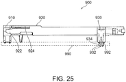
Fig. 25 , an IC card connector (connector) 900 disclosed inPatent Document 1 comprises ahousing 910 and aframe 920 each of which is to be attached to acircuit board 990. Theframe 920 hasengagement pieces 922 and anupper plate portion 924. Theframe 920 holdsground terminals 930. Each of theground terminals 930 has twoengagement lugs 932. Each of theengagement lugs 932 is formed with a projectingend 934. Thecircuit board 990 is formed withattachment holes 992. When theconnector 900 is attached to thecircuit board 990, first of all, thehousing 910 is fixed to thecircuit board 990. Next, theengagement pieces 922 and theupper plate portion 924 of theframe 920 are attached to thehousing 910, and theengagement lugs 932 of theground terminal 930 are then inserted into each of theattachment holes 992. Each of the projecting ends 934 of theengagement lugs 932 is pressed to a wall surface of each of theattachment holes 990, so that theframe 920 is attached to thecircuit board 990. - Patent Document 1:
JP A 2002-75496 - In a case, for example, where the
connector 900 ofPatent Document 1 is attached to thecircuit board 990 having a thin thickness, theframe 920 might be unstable. Accordingly, it is necessary to fix theengagement lugs 932 to thecircuit board 990 by soldering or the like after theframe 920 is attached to thecircuit board 990. In other words, it is difficult to apply theframe 920 ofPatent Document 1 to each of circuit boards having various thicknesses. - It is therefore an object of the present invention to provide a connector which is attachable to an object such as a circuit or the like and which enables a frame to be more stably attached to each of objects having various thicknesses.
- An aspect of the present invention provides a connector attachable to an object having a lock portion. The connector comprises a housing and a frame. The housing has a press portion and a support portion. The housing is fixed to the object under an attached state where the connector is attached to the object. The frame has a supported portion, a pressed portion and a locked portion. When the connector is in the attached state, the supported portion is positioned between the pressed portion and the locked portion in a front-rear direction and is supported from below by the support portion in an up-down direction perpendicular to the front-rear direction. Under the attached state, the pressed portion is pressed by the press portion from above. Under the attached state, the locked portion applies a force to the lock portion from below.
- Another aspect of the present invention provides an electronic equipment in which the connector is installed.
- According to the present invention, under the attached state where the connector is attached thereto, the locked portion of the frame applies force to the lock portion of the object from below. In other words, the locked portion is pressed on the lock portion. Accordingly, even if a position of the lock portion in the up-down direction is different from its design value, the locked portion is locked by the lock portion. Especially, if the lock portion is positioned in the vicinity of a lower end of an attachment hole of an object, the locked portion can be locked by the lock portion even in a case where thicknesses of objects are varied. The frame of the connector according to the present invention can be more stably attached to each of objects having various thicknesses.
- An appreciation of the objectives of the present invention and a more complete understanding of its structure may be had by studying the following description of the preferred embodiment and by referring to the accompanying drawings.
-
-
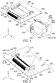
Fig. 1 is a perspective view showing a connector according to an embodiment of the present invention. The connector is in an attached state where the connector is attached to a circuit board. The connector is illustrated so that the vicinity of a supported portion of a frame is cut away. The vicinity of the supported portion (a part enclosed by dashed line) is shown enlarged. -
Fig. 2 is a perspective view showing a housing of the connector ofFig. 1 . The housing is fixed on the circuit board. -
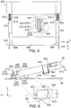
Fig. 3 is a perspective view showing the frame of the connector ofFig. 1 . The frame is not attached to the housing while being positioned at a horizontal position. A part of a front end portion of the frame (a part enclosed by dashed line) is shown enlarged. -
Fig. 4 is a front view showing the frame ofFig. 3 . The vicinity of a side plate portion of the frame (a part enclosed by dashed line) is shown enlarged. -
Fig. 5 is a bottom view showing the frame ofFig. 3 . The vicinity of a hook of the frame (a part enclosed by dashed line) is shown enlarged. -
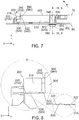
Fig. 6 is a side view showing the housing and the frame ofFig. 1 . The frame is positioned at a tilted position which the frame begins to be attached to the housing. The vicinity of an overhanging portion of the housing (a part enclosed by dashed line) is shown enlarged. -
Fig. 7 is a side view showing the housing and the frame ofFig. 1 . -
Fig. 8 is a side view showing the vicinity of the overhanging portion of the housing ofFig. 7 (a part enclosed by dashed line A). The vicinity of a press portion of the housing (a part enclosed by dashed line) is shown further enlarged. -
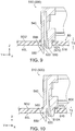
Fig. 9 is a cross-sectional view showing the side plate portion of the frame of the connector ofFig. 7 , taken along line IX-IX. The frame is attached to a first circuit board. -
Fig. 10 is a cross-sectional view showing the side plate portion of the frame of the connector ofFig. 7 , taken along line X-X. The frame is attached to a second circuit board. -
Fig. 11 is a perspective view showing a modification of the frame ofFig. 3 . The vicinity of a hook of the frame (a part enclosed by dashed line) is shown enlarged. -
Fig. 12 is a rear view showing the frame ofFig. 11 . The vicinity of a side plate portion of the frame (a part enclosed by dashed line) is shown enlarged. -
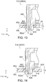
Fig. 13 is a cross-sectional view showing the side plate portion of the frame ofFig. 11 . The frame is attached to the first circuit board. -
Fig. 14 is another cross-sectional view showing the side plate portion of the frame ofFig. 11 . The frame is attached to the second circuit board. -
Fig. 15 is a cross-sectional view showing a side plate portion of another modification of the frame ofFig. 3 . The frame is attached to the first circuit board. -
Fig. 16 is another cross-sectional view showing the side plate portion of the frame ofFig. 15 . The frame is attached to the second circuit board. -
Fig. 17 is a cross-sectional view showing a side plate portion of yet another modification of the frame ofFig. 3 . The frame is attached to the first circuit board. The vicinity of a locked portion (a part enclosed by dashed line) is shown enlarged. -
Fig. 18 is another cross-sectional view showing the side plate portion of the frame ofFig. 17 . The frame is attached to the second circuit board. -
Fig. 19 is a cross-sectional view showing a side plate portion of still another modification of the frame ofFig. 3 . The frame is attached to the first circuit board. -
Fig. 20 is another cross-sectional view showing the side plate portion of the frame ofFig. 19 . The frame is attached to the second circuit board. -
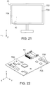
Fig. 21 is a front view showing an electronic equipment in which the connector ofFig. 1 is installed. An outline of a circuit board, which is arranged inside the electronic equipment, and an outline of the connector, which is attached to the circuit board, are illustrated by dashed line therein. -
Fig. 22 is a perspective view showing the circuit board ofFig. 21 . -
Fig. 23 is a perspective view showing another electronic equipment in which the connector ofFig. 1 is installed. An outline of a circuit board, which is arranged inside the electronic equipment, and an outline of the connector, which is attached to the circuit board, are illustrated by dashed line therein. -
Fig. 24 is a perspective view showing the circuit board ofFig. 23 . -
Fig. 25 is a side view showing a connector ofPatent Document 1. - While the invention is susceptible to various modifications and alternative forms, specific embodiments thereof are shown by way of example in the drawings and will herein be described in detail. It should be understood, however, that the drawings and detailed description thereto are not intended to limit the invention to the particular form disclosed, but on the contrary, the intention is to cover all modifications, equivalents and alternatives falling within the spirit and scope of the present invention as defined by the appended claims.
- As shown in
Fig. 1 , aconnector 10 according to an embodiment of the present invention is an on-board connector which is attachable to an object (circuit board) 80. In addition, theconnector 10 according to the present embodiment is a card connector which is connectable to a connecting object (not shown) such as a card or the like. However, the present invention is also applicable to a connector other than the card connector. - As shown in
Fig. 2 , thecircuit board 80 has anupper surface 80U and alower surface 80L in an up-down direction (Z-direction). Each of theupper surface 80U and thelower surface 80L is perpendicular to the Z-direction. Thecircuit board 80 according to the present embodiment is formed with two attachment holes 810. Each of the attachment holes 810 pierces thecircuit board 80 in the Z-direction. - As shown in
Fig. 1 , theconnector 10 according to the present embodiment comprises ahousing 200 made of insulating material, twoholddowns 300 each made of conductive material, a plurality ofcontacts 400 each made of conductive material and aframe 500 made of insulating material. In particular, each of thehousing 200 and theframe 500 according to the present embodiment is made of resin. - As shown in
Fig. 2 , thehousing 200 according to the present embodiment has a holdingportion 210 and twoarm portions 230. The holdingportion 210 extends long in a Y-direction (width direction). The holdingportion 210 has twoside portions 214. Theside portions 214 are positioned at opposite ends, respectively, of the holdingportion 210 in the Y-direction. Thearm portions 230 extend rearward (in a negative X-direction) from theside portions 214, respectively, in an X-direction (front-rear direction). Each of thearm portions 230 has an upper surface (support surface) 232. Thus, thehousing 200 has two of the support surfaces 232. Thesupport surface 232 is perpendicular to the Z-direction. The support surfaces 232 according to the present embodiment are formed to be flush with upper surfaces of theside portions 214, respectively. - The
housing 200 according to the present embodiment has two overhangingportions 216. The overhangingportions 216 are formed at side surfaces of theside portions 214, respectively, in the Y-direction. Each of the overhangingportions 216 overhangs outward in the Y-direction from an upper portion (positive Z-side portion) of thecorresponding side portion 214. Each of the overhangingportions 216 has alower surface 218. Thelower surface 218 is perpendicular to the Z-direction. When theconnector 10 is in an attached state where theconnector 10 is attached to thecircuit board 80, the support surfaces 232 of the arm portions 230 (housing 200) are positioned above (in a positive Z-direction beyond) thelower surfaces 218 of the overhangingportions 216, respectively. - The
holddowns 300 are held by thearm portions 230, respectively, of thehousing 200. Thecontacts 400 are held by the holdingportion 210 of thehousing 200 and are arranged in the Y-direction. Under the attached state, theholddowns 300 and thecontacts 400 are fixed to theupper surface 80U of thecircuit board 80 by soldering or the like. Accordingly, thehousing 200 according to the present embodiment is attached and fixed on theupper surface 80U of thecircuit board 80 by the holddowns 300 and thecontacts 400. However, thehousing 200 may be attached to thecircuit board 80 by other means. - As shown in
Fig. 3 , theframe 500 according to the present embodiment has twoside plate portions 510, twofront end portions 520, two projectingportions 524 and anupper plate portion 580. - Referring to
Figs. 1 and3 , each of theside plate portions 510 extends long in the X-direction under the attached state (seeFig. 1 ). Under the attached state, thefront end portions 520 project forward (in a positive X-direction) from lower portions (negative Z-side portions) of front ends (positive X-side ends) of theside plate portions 510, respectively. Each of thefront end portions 520 has anupper surface 522. Under the attached state, theupper surface 522 is almost perpendicular to the Z-direction. The projectingportions 524 are provided on theupper surfaces 522, respectively. The projectingportions 524 project upward (in the positive Z-direction) from theupper surfaces 522, respectively. - The
upper plate portion 580 couples the twoside plate portions 510 with each other in the Y-direction. Theupper plate portion 580 has two lower surfaces (supported surfaces) 584. The supported surfaces 584 are positioned at opposite sides, respectively, of theupper plate portion 580 in the Y-direction. Under the attached state (seeFig. 1 ), each of the supported surfaces 584 is almost perpendicular to the Z-direction. Under the attached state, the supportedsurfaces 584 are positioned above the support surfaces 232, respectively, of the housing 200 (seeFig. 1 ). - As shown in
Figs. 3, 4 and9 , each of theside plate portions 510 is provided with acontact surface 516, aspring portion 540 and apositioning portion 570. Thecontact surface 516 is perpendicular to the Z-direction. Under the attached state, thecontact surface 516 is positioned at a lower end (an end in a negative Z-direction) of theside plate portion 510 except thespring portion 540 and thepositioning portion 570. Under the attached state, thespring portion 540 extends in the Z-direction. Thespring portion 540 is resiliently deformable in the Y-direction. Each of thespring portions 540 is provided with ahook 550. Thehook 550 is positioned at a lower end part (an end part in the negative Z-direction) of thespring portion 540 and projects outward in the Y-direction. Thehook 550 is movable in the Y-direction by resilient deformation of thespring portion 540. Under the attached state, thepositioning portion 570 extends downward from thecontact surface 516. - As shown in
Fig. 5 , thepositioning portion 570 according to the present embodiment has twobent portions 572 and acoupling portion 574 which couples thebent portions 572 with each other. Thepositioning portion 570 according the present embodiment is positioned inward of a lockedportion 560 in the Y-direction. However, a part of the positioning portion 570 (for example, a part of the bent portion 572) may be positioned outward of the lockedportion 560 in the Y-direction. In other words, it is sufficient that at least a part of thepositioning portion 570 is positioned inward of the lockedportion 560 in the Y-direction. The thus-configuredpositioning portion 570 can prevent thespring portion 540 from being excessively resiliently deformed inward in the Y-direction to be broken. - As shown in
Figs. 3 ,7 and 8 , theframe 500 has two pressedportions 530 and two supportedportions 590. According to the present embodiment, the pressedportions 530 are upper ends (positive Z-side ends) of the projectingportions 524, respectively, and the supportedportions 590 are edges of the supportedsurfaces 584, respectively, of theupper plate portion 580. - As shown in
Figs. 1 ,7 and 8 , thehousing 200 has twopress portions 220 and twosupport portions 240. According to the present embodiment, thepress portions 220 are parts of thelower surfaces 218 of the overhangingportions 216, respectively, and thesupport portions 240 are parts of the support surfaces 232, respectively, of thehousing 200. However, thesupport portion 240 may be any part of thehousing 200, provided that the part can support the supportedportion 590 from below under the attached state. Thepress portion 220 may be any part of thehousing 200, provided that the part can press the pressedportion 530 from above under the attached state. - As shown in
Figs. 3, 4 and7 , theframe 500 has two of the lockedportions 560. The lockedportions 560 are locked to thecircuit board 80 under the attached state. The lockedportions 560 according to the present embodiment are surfaces of thehooks 550, respectively. Under the attached state, each of the lockedportions 560 according to the present embodiment extends in an XY-plane perpendicular to the Z-direction (up-down direction). Thus, each of the lockedportions 560 extends in the Y-direction. However, it is enough that the lockedportion 560 extends in a direction intersecting with the Z-direction under the attached state as a whole. - As understood from
Figs. 6 and7 , under a state where thehousing 200 is fixed to thecircuit board 80, theframe 500 is attached to thehousing 200 and thecircuit board 80 by a positioning operation followed by a rotating operation. In detail, first, the positioning operation causes that the pressedportions 530 are positioned below thepress portions 220, respectively, while the supportedportions 590 are positioned above thesupport portions 240, respectively. Accordingly, theframe 500 is positioned at a tilted position (a position shown inFig. 6 ) where theframe 500 is tilted with respect to thehousing 200. Next, a negative X-side portion of theframe 500 is pressed downward so that theframe 500 is rotated along a rotational direction Rn (seeFig. 6 ) toward a horizontal position (a position shown inFig. 7 ) where theframe 500 extends horizontally with respect to thehousing 200. In other words, the rotating operation rotates theframe 500 from the tilted position toward the horizontal position. - As shown in
Fig. 6 , when thehousing 200 is fixed to thecircuit board 80 while theframe 500 is not attached to thehousing 200, thesupport portion 240 and thepress portion 220 are spaced apart from each other by a distance (D1) in the Z-direction. As understood fromFigs. 6 and7 , when theframe 500 is positioned at the horizontal position without being attached to thehousing 200, the supportedportion 590 and the pressedportion 530 are spaced apart from each other by a distance (D2) in the Z-direction. According to the present embodiment, the distance (D1) is greater than the distance (D2). Thus, upon the aforementioned rotating operation, the pressedportion 530 receives a downward force by each of thepress portions 220 so that a portion of theframe 500, which is positioned beyond the supportedportion 590 in the negative X-direction, receives an upward momentum. Theframe 500 can be attached to thehousing 200 by being rotated as described above while resisting the momentum. - As understood from
Figs. 7 and9 , when theframe 500 is moved to the horizontal position by the aforementioned rotating operation, thehooks 550 pass through the attachment holes 810, respectively, of thecircuit board 80 while being moved inward in the Y-direction. When each of thehooks 550 reaches below thecircuit board 80, each of thehooks 550 is moved outward in the Y-direction. Accordingly, each of the lockedportions 560 is positioned below thelower surface 80L of thecircuit board 80. - As shown in
Fig. 7 , when theconnector 10 is in the attached state, the supportedportions 590 are positioned between each of the pressedportions 530 and each of the lockedportions 560 in the X-direction. Under the attached state, the supportedportions 590 are supported from below by thesupport portions 240, respectively, in the Z-direction. In addition, since the distance (D1) is greater than the distance (D2) as described above (seeFig. 6 ), the pressedportion 530 is pressed by each of thepress portions 220 from above under the attached state. Accordingly, under the attached state, each of the lockedportions 560 receives a momentum along a reverse rotational direction Rr. As a result, each of the lockedportions 560 is pressed against thelower surface 80L of thecircuit board 80 from below under the attached state. Each of the pressedportions 530, the lockedportions 560 and the supportedportions 590 may be any part of theframe 500, 2provided that each of the pressedportions 530, the lockedportions 560 and the supportedportions 590 is formed as described above. - As understood from
Fig. 9 , parts of thelower surface 80L are pressed upward by the lockedportions 560, respectively. The parts of thelower surface 80L function aslock portions 820 which lock the lockedportions 560, respectively. In other words, thecircuit board 80 has thelock portions 820. Under the attached state, the lockedportions 560 are brought into contact with thelock portions 820 from below to apply forces to thelock portions 820, respectively, from below. Accordingly, theframe 500 is stably attached to thecircuit board 80. For example, theframe 500 is prevented from being unstable. Especially, the lockedportions 560 according to the present embodiment are provided on theside plate portions 510, respectively, of theframe 500. Thus, theframe 500 can be more securely prevented from being unstable. - As shown in
Figs. 7 and9 , under the attached state, the positioningportions 570 are partially inserted into the attachment holes 810, respectively. The twopositioning portions 570, which are inserted into the attachment holes 810, carry out positioning of the lockedportions 560, respectively, in the X-direction and in the Y-direction. According to the present embodiment, thebent portions 572 of thepositioning portion 570 perform positioning of each of the lockedportions 560 in the X-direction (seeFig. 7 ), and thecoupling portion 574 performs positioning of each of the lockedportions 560 in the Y-direction (seeFig. 9 ). - As shown in
Fig. 10 , the thus-configuredconnector 10 is attachable to a circuit board (object) 80X (second circuit board) which is different from the circuit board 80 (first circuit board). In detail, as shown inFigs. 9 and 10 , thecircuit board 80 has a thickness (T1), and thecircuit board 80X has a thickness (T2). The thickness (T2) is greater than the thickness (T1). Thecircuit board 80X is formed withattachment holes 810X which are similar to the attachment holes 810. However, a size of each of the attachment holes 810X in the Z-direction is equal to the thickness (T2). Accordingly, the size of each of the attachment holes 810X in the Z-direction is greater than a size of each of the attachment holes 810 in the Z-direction. - Under the attached state, the locked
portion 560 of theframe 500 applies a force to each oflock portions 820 of thecircuit board 80X from below. Accordingly, theframe 500 can be stably attached also to thecircuit board 80X which is thicker than thecircuit board 80. Thus, even if, for example, a position of each of thelock portions 820 in the Z-direction is different from each of their design values, the lockedportions 560 are locked by thelock portions 820, respectively. Theframe 500 according to the present embodiment can be more stably attached to each of objects having various thicknesses. - As understood from
Figs. 9 and 10 , a shape of the lockedportion 560 can be modified variously. For example, the lockedportion 560 may not be a plane parallel to the XY-plane, but may extend outward in the Y-direction while being tilted upward. In this case, an end portion of the lockedportion 560, which is positioned outward in the Y-direction, is locked by alock portion 820 which is a part of thelower surface 80L. - Hereafter, explanation is made about various modifications of the locked
portion 560. In the various modifications as described below, members and portions other than the locked portion have structures same as those of the present embodiment. Accordingly, in the following explanation, explanation is made only about members and portions which are directly related to the locked portion. - As shown in
Figs. 11 and 12 , aframe 500A according to a first modification hashooks 550A which are slightly different from the hooks 550 (seeFig. 3 ). Each of thehooks 550A has a lockedportion 560A. Unlike the lockedportion 560, the lockedportion 560A has twoslope portions 562. - As shown in
Figs. 13 and 14 , when theconnector 10 having the lockedportions 560A is attached to the circuit board 80 (or thecircuit board 80X) (seeFig. 1 ), one of theslope portions 562 of the lockedportion 560A is brought into contact with a lower end (an end in the negative Z-direction) of a wall surface of each of the attachment holes 810 (or the attachment holes 810X) from below. The one of theslope portions 562 presses the lower end from below, so that the one of theslope portions 562 is locked. In other words, alock portion 820 according to the first modification is the lower end of the wall surface of each of the attachment holes 810 (or the attachment holes 810X). - According to the first modification, one of the
slope portions 562 of the lockedportion 560A is brought into contact with each of thelock portions 820 from below under the attached state. Theslope portion 562 is oblique to the Z-direction when theslope portion 562 is brought into contact with each of thelock portions 820. The number of theslope portions 562 according to the first modification is two. However, it is sufficient that the number of theslope portions 562 is one or more. In other words, it is sufficient that the lockedportion 560A has one or more of theslope portions 562. - As shown in
Figs. 15 and 16 , aframe 500B according to a second modification hashooks 550B which are slightly different from the hooks 550 (seeFig. 3 ). Each of thehooks 550B has a lockedportion 560B. Unlike the lockedportion 560, the lockedportion 560B has acurved portion 564. Thecurved portion 564 is curved in a YZ-plane. - When the
connector 10 having the lockedportions 560B is attached to the circuit board 80 (or thecircuit board 80X) (seeFig. 1 ), thecurved portion 564 of the lockedportion 560B is brought into contact with the lower end of the wall surface of each of the attachment holes 810 (or the attachment holes 810X) from below. Thecurved portion 564 presses the lower end from below, so that thecurved portion 564 is locked. In other words, alock portion 820 according to the second modification is the lower end of the wall surface of each of the attachment holes 810 (or the attachment holes 810X). According to the second modification, thecurved portion 564 is brought into contact with each of thelock portions 820 from below under the attached state. - The number of the
curved portion 564 of the lockedportion 560B according to the second modification is one. However, it is sufficient that the number of thecurved portions 564 is one or more. In other words, it is sufficient that the lockedportion 560B has one or more of thecurved portions 564. - As shown in
Figs. 17 and 18 , aframe 500C according to a third modification hashooks 550C which are slightly different from thehooks 550B (seeFigs. 15 and 16 ). Each of thehooks 550C has a lockedportion 560C. Unlike the lockedportion 560B, the lockedportion 560C further has aslope portion 562 which is oblique to the Z-direction. - As shown in
Fig. 17 , when theconnector 10 having the lockedportions 560C is attached to the circuit board 80 (seeFig. 1 ), theslope portion 562 of the lockedportion 560C is brought into contact with the lower end of the wall surface of each of the attachment holes 810 from below. Theslope portion 562 presses the lower end from below, so that theslope portion 562 is locked. In addition, as shown inFig. 18 , when theconnector 10 is attached to thecircuit board 80X, thecurved portion 564 of the lockedportion 560C is brought into contact with the lower end of the wall surface of each of the attachment holes 810 from below. Thecurved portion 564 presses the lower end from below, so that thecurved portion 564 is locked. In other words, alock portion 820 according to the third modification is the lower end of the wall surface of each of the attachment holes 810. - The number of the
slope portion 562 of the lockedportion 560C according to the third modification is one. However, it is sufficient that the number of theslope portions 562 is one or more. In other words, it is sufficient that the lockedportion 560B has one or more of theslope portions 562. In addition, it is sufficient that one of thecurved portions 564 or one of theslope portions 562 is brought into contact with thelock portion 820 from below under the attached state. - As shown in
Figs. 19 and 20 , aframe 500D according to a fourth modification hashooks 550D which are slightly different from the hooks 550 (seeFig. 3 ). Each of thehooks 550D has a lockedportion 560D. Unlike the lockedportion 560, the lockedportion 560D has a stair shape in the YZ-plane. - When the
connector 10 having the lockedportions 560D is attached to the circuit board 80 (seeFig. 1 ), a part of the stair shape of each of the lockedportions 560D is brought into contact with thelower surface 80L of thecircuit board 80 from below. The lockedportion 560D presses thelower surface 80L from below, so that the lockedportion 560D is locked. In addition, as shown inFig. 20 , when theconnector 10 is attached to thecircuit board 80X, another part of the stair shape of the lockedportion 560D is brought into contact with the lower end of wall surface of each of the attachment holes 810 from below. The lockedportion 560D presses the lower end from below, so that the lockedportion 560D is locked. In other words, alock portion 820 according to the fourth modification is thelower surface 80L of thecircuit board 80 or the lower end of the wall surface of each of the attachment holes 810. According to the fourth modification, a part of the stair shape of the lockedportion 560D is brought into contact with each of thelock portions 820 from below under the attached state. - As shown in
Figs. 13 to 20 , according to the first to fourth modifications, the locked portions are surfaces of the hooks, respectively, similar to the lockedportion 560. Under the attached state, each of the locked portions, as a whole, extends in a direction which intersects with the Z-direction. - As shown in
Figs. 9 and 10 , when theframe 500 according to the present embodiment is attached to thecircuit board 80 having a thin thickness, thecontact surface 516 of each of theside plate portions 510 is positioned apart from and above theupper surface 80U of thecircuit board 80. Accordingly, if, for example, vibration is applied to theframe 500, theframe 500 might be unstable. On the other hand, as shown inFigs. 13 to 20 , according to the first to fourth modifications, each of the locked portions can be locked while thecontact surface 516 of each of theside plate portions 510 is brought into contact with theupper surface 80U when the frame is attached to any of thecircuit board 80 and thecircuit board 80X. In other words, according to the first to fourth modifications, the frame can be more stably attached to any of thecircuit board 80 and thecircuit board 80X. - The
connector 10 according to the present embodiment can be further variously modified in addition to the above-explained modifications. For example, as shown inFigs. 9, 10 and13 to 20 , each of the lock portions according to the present embodiment and the modifications is positioned in the vicinity of the lower end of the attachment hole. Under the attached state, the locked portion is inserted into each of the attachment holes. Furthermore, at least a part of the locked portion projects downward from the lower end of each of the attachment holes. However, the lock portion may not be a portion which is positioned in the vicinity of the attachment hole. The lock portion may be, for example, an edge of a notch (not shown) which is formed on the circuit board. In addition, the lock portion may be a part of a member (not shown) which is provided on a circuit board. However, in order to easily form the lock portion, it is preferable that the lock portion is a portion which is positioned in the vicinity of the attachment hole. - The
connector 10 according to the present embodiment is installable in various electronic equipments as described below. - Referring to
Figs. 21 and 22 , a television receiver (electronic equipment) 70 comprises ahousing 702, adisplay panel 704 and an object (circuit board) 706. Thedisplay panel 704 is attached to thehousing 702 so as to be able to display images and videos. Thedisplay panel 704 can be formed by using, for example, a liquid crystal display, an organic EL (Electro Luminescence) display or a plasma display. Thecircuit board 706 is attached inside thehousing 702. - Referring to
Fig. 22 , thecircuit board 706 is similar to the circuit board 80 (seeFig. 2 ) and has a structure to which theconnector 10 is attachable. In addition to theconnector 10, variouselectronic devices 708 are attached to thecircuit board 706. Theconnector 10 installed in theelectronic equipment 70 as described above is used for, for example, inputting images, which are to be displayed on thedisplay panel 704, thereto from a memory card (not shown). - Referring to
Figs. 23 and 24 , anelectronic equipment 72, which is a PC (Personal Computer), comprises an object (circuit board) 726. Thecircuit board 726 is attached inside theelectronic equipment 72. - Referring to
Fig. 24 , thecircuit board 726 is similar to the circuit board 80 (seeFig. 2 ) and has a structure to which theconnector 10 is attachable. Only theconnector 10 is attached to the illustratedcircuit board 726. However, an electronic equipment other than theconnector 10 may be attached to thecircuit board 726. Theelectronic equipment 72 can receive/output data from/to an external card (not shown) by installing theconnector 10 in theelectronic equipment 72. - The present application is based on a Japanese patent application of
JP2014-086371 - While there has been described what is believed to be the preferred embodiment of the invention, those skilled in the art will recognize that other and further modifications may be made thereto without departing from the spirit of the invention, and it is intended to claim all such embodiments that fall within the true scope of the invention.
-
- 10
- connector
- 200
- housing
- 210
- holding portion
- 214
- side portion
- 216
- overhanging portion
- 218
- lower surface
- 220
- press portion
- 230
- arm portion
- 232
- upper surface (support surface)
- 240
- support portion
- 300
- holddown
- 400
- contact
- 500, 500A, 500B, 500C, 500D
- frame
- 510
- side plate portion
- 516
- contact surface
- 520
- front end portion
- 522
- upper surface
- 524
- projecting portion
- 530
- pressed portion
- 540
- spring portion
- 550, 550A, 550B, 550C, 550D
- hook
- 560, 560A, 560B, 560C, 650D
- locked portion
- 562
- slope portion
- 564
- curved portion
- 570
- positioning portion
- 572
- bent portion
- 574
- coupling portion
- 580
- upper plate portion
- 584
- lower surface (supported surface)
- 590
- supported portion
- 70
- television receiver (electronic equipment)
- 702
- housing
- 704
- display panel
- 706
- object (circuit board)
- 708
- electronic device
- 72
- PC (electronic equipment)
- 726
- object (circuit board)
- 80, 80X
- object (circuit board)
- 80U
- upper surface
- 80L
- lower surface
- 810, 810X
- attachment hole
- 820
- lock portion
- 900
- IC card connector (connector)
- 910
- housing
- 920
- frame
- 922
- engagement piece
- 924
- upper plate portion
- 930
- ground terminal
- 932
- engagement lug
- 934
- projecting end
- 990
- circuit board
- 992
- attachment hole
Claims (14)
- A connector attachable to an object having a lock portion, the connector comprising a housing and a frame, wherein:the housing has a press portion and a support portion;the housing is fixed to the object under an attached state where the connector is attached to the object;the frame has a supported portion, a pressed portion and a locked portion;when the connector is in the attached state, the supported portion is positioned between the pressed portion and the locked portion in a front-rear direction and is supported from below by the support portion in an up-down direction perpendicular to the front-rear direction;under the attached state, the pressed portion is pressed by the press portion from above; andunder the attached state, the locked portion applies a force to the lock portion from below.
- The connector as recited in claim 1, wherein:under a state where the housing is fixed to the object, the frame is attached to the housing by a positioning operation followed by a rotating operation;the positioning operation causes that the pressed portion is positioned below the press portion while the supported portion is positioned above the support portion;the rotating operation rotates the frame from a tilted position, where the frame is tilted with respect to the housing, toward a horizontal position where the frame extends horizontally with respect to the housing; andwhen the housing is fixed to the object while the frame is positioned at the horizontal position without being attached to the housing, a distance between the support portion and the press portion in the up-down direction is greater than another distance between the supported portion and the pressed portion in the up-down direction.
- The connector as recited in claim 1 or 2, wherein:the frame has a projecting portion; andwhen the connector is in the attached state, the projecting portion projects upward in the up-down direction while the pressed portion is an upper end of the projecting portion.
- The connector as recited in claim 3, wherein:the housing has an overhanging portion and a support surface;the overhanging portion extends outward in a width direction, which is perpendicular to both the up-down direction and the front-rear direction, to have a lower surface;the press portion is a part of the lower surface of the overhanging portion;when the connector is in the attached state, the support surface of the housing is positioned above the lower surface of the overhanging portion in the up-down direction;the support portion is a part of the support surface of the housing;the frame has a front end portion and an upper plate portion;the front end portion has an upper surface;the projecting portion is provided on the upper surface of the front end portion and projects upward from the upper surface of the front end portion under the attached state;the upper plate portion has a supported surface;under the attached state, the supported surface of the upper plate portion is positioned above the support surface of the housing; andthe supported portion is an edge of the supported surface of the upper plate portion.
- The connector as recited in one of claims 1 to 4, wherein:the object has an attachment hole which pierces the object in the up-down direction;the lock portion is positioned in the vicinity of a lower end of the attachment hole; andunder the attached state, the locked portion is inserted into the attachment hole while at least a part of the locked portion projects downward from the lower end of the attachment hole.
- The connector as recited in claim 5, wherein:the frame has a hook;the locked portion is a surface of the hook; andunder the attached state, the locked portion as a whole extends in a direction intersecting with the up-down direction.
- The connector as recited in claim 6, wherein:under the attached state, the locked portion extends in a direction perpendicular to the up-down direction; andunder the attached state, the locked portion is brought into contact with the lock portion from below.
- The connector as recited in claim 6, wherein:the locked portion has one or more slope portions; andunder the attached state, one of the slope portions of the locked portion is oblique to the up-down direction and is brought into contact with the lock portion from below.
- The connector as recited in claim 6, wherein:the locked portion has one or more curved portions each of which is curved in a plane defined by the up-down direction and the front-rear direction; andunder the attached state, one of the curved portions of the locked portion is brought into contact with the lock portion from below.
- The connector as recited in claim 9, wherein:the locked portion has one or more slope portions each of which is oblique to the up-down direction; andunder the attached state, one of the curved portions or one of the slope portions of the locked portion is brought into contact with the lock portion from below.
- The connector as recited in claims 6, wherein:the locked portion has a stair shape in a plane defined by the up-down direction and the front-rear direction; andunder the attached state, a part of the stair shape is brought into contact with the lock portion from below.
- The connector as recited in one of claims 5 to 11, wherein:the frame has a positioning portion; andunder the attached state, the positioning portion is inserted into the attachment hole while carrying out positioning of the locked portion in the front-rear direction.
- The connector as recited in claim 12, wherein
at least a part of the positioning portion is positioned inward of the locked portion in a width direction perpendicular to both the up-down direction and the front-rear direction. - An electronic equipment in which the connector as recited in one of claims 1 to 13 is installed.
Applications Claiming Priority (2)
| Application Number | Priority Date | Filing Date | Title |
|---|---|---|---|
| JP2014086371A JP5813817B1 (en) | 2014-04-18 | 2014-04-18 | Connectors and electronic devices |
| PCT/JP2015/060062 WO2015159701A1 (en) | 2014-04-18 | 2015-03-31 | Connector and electronic equipment |
Publications (3)
| Publication Number | Publication Date |
|---|---|
| EP3121906A1 true EP3121906A1 (en) | 2017-01-25 |
| EP3121906A4 EP3121906A4 (en) | 2017-11-15 |
| EP3121906B1 EP3121906B1 (en) | 2019-05-08 |
Family
ID=54323912
Family Applications (1)
| Application Number | Title | Priority Date | Filing Date |
|---|---|---|---|
| EP15779608.7A Active EP3121906B1 (en) | 2014-04-18 | 2015-03-31 | Connector and electronic equipment |
Country Status (7)
| Country | Link |
|---|---|
| US (1) | US9819104B2 (en) |
| EP (1) | EP3121906B1 (en) |
| JP (1) | JP5813817B1 (en) |
| CN (1) | CN107078424B (en) |
| MY (1) | MY178215A (en) |
| TW (1) | TWI628886B (en) |
| WO (1) | WO2015159701A1 (en) |
Families Citing this family (1)
| Publication number | Priority date | Publication date | Assignee | Title |
|---|---|---|---|---|
| JP6706864B2 (en) * | 2016-05-26 | 2020-06-10 | 古河電気工業株式会社 | Rotating connector and fixing structure of rotating connector |
Family Cites Families (12)
| Publication number | Priority date | Publication date | Assignee | Title |
|---|---|---|---|---|
| EP0520080B2 (en) * | 1991-06-28 | 2005-03-30 | Molex Incorporated | IC card connector |
| JPH0585099U (en) | 1992-04-16 | 1993-11-16 | ソニー株式会社 | Parts mounting device |
| US5275573A (en) * | 1992-11-16 | 1994-01-04 | The Whitaker Corporation | Electrical connector eject mechanism |
| US5613860A (en) * | 1994-12-14 | 1997-03-25 | Molex Incorporated | Universal grounding clip for card-receiving connector |
| JPH11297415A (en) * | 1998-04-03 | 1999-10-29 | Molex Inc | Card connector |
| JP3252259B2 (en) | 1998-07-17 | 2002-02-04 | 日本航空電子工業株式会社 | Card connector |
| US6220882B1 (en) * | 1999-11-15 | 2001-04-24 | Molex Incorporated | IC card connector with release means |
| JP2002075496A (en) * | 2000-08-31 | 2002-03-15 | Alps Electric Co Ltd | IC card connector |
| JP3779867B2 (en) * | 2000-08-31 | 2006-05-31 | アルプス電気株式会社 | Ground terminal and IC card connector using the same |
| JP2002151191A (en) | 2000-11-09 | 2002-05-24 | Iriso Denshi Kogyo Kk | Electrical connector |
| TWM297565U (en) * | 2006-01-23 | 2006-09-11 | Amphenol Taiwan Corp | Micro socket connector |
| TWM378512U (en) | 2009-10-19 | 2010-04-11 | Wieson Technologies Co Ltd | Card connector and electrical connector assembly |
-
2014
- 2014-04-18 JP JP2014086371A patent/JP5813817B1/en not_active Expired - Fee Related
-
2015
- 2015-03-31 MY MYPI2016703755A patent/MY178215A/en unknown
- 2015-03-31 WO PCT/JP2015/060062 patent/WO2015159701A1/en not_active Ceased
- 2015-03-31 US US15/302,969 patent/US9819104B2/en active Active
- 2015-03-31 CN CN201580020395.4A patent/CN107078424B/en active Active
- 2015-03-31 EP EP15779608.7A patent/EP3121906B1/en active Active
- 2015-04-07 TW TW104111073A patent/TWI628886B/en active
Also Published As
| Publication number | Publication date |
|---|---|
| WO2015159701A1 (en) | 2015-10-22 |
| CN107078424A (en) | 2017-08-18 |
| US9819104B2 (en) | 2017-11-14 |
| US20170033477A1 (en) | 2017-02-02 |
| MY178215A (en) | 2020-10-07 |
| TWI628886B (en) | 2018-07-01 |
| JP2015207404A (en) | 2015-11-19 |
| JP5813817B1 (en) | 2015-11-17 |
| EP3121906A4 (en) | 2017-11-15 |
| EP3121906B1 (en) | 2019-05-08 |
| CN107078424B (en) | 2019-06-11 |
| TW201547132A (en) | 2015-12-16 |
Similar Documents
| Publication | Publication Date | Title |
|---|---|---|
| CN102651519B (en) | Connector apparatus | |
| TWI552448B (en) | Connector | |
| US7361043B2 (en) | Apparatus including card element, device inserted into apparatus and a method for connecting or disconnecting the card element | |
| US9060441B2 (en) | Electronic device and power supply positioining apparatus thereof | |
| US20170005422A1 (en) | Connector component | |
| CN113994293B (en) | Information processing device | |
| US9979122B1 (en) | Electronic device and connector | |
| CN104202942B (en) | Printer | |
| US6527562B2 (en) | PCI expansion adapter with PC card slot and electronic apparatus provided with the same | |
| US8029314B2 (en) | Connector for mounting a flexible printed circuit board | |
| EP3121906B1 (en) | Connector and electronic equipment | |
| CN102385423B (en) | Electronic installation | |
| JP6281698B2 (en) | Connector device | |
| US9276341B2 (en) | Connector and connector assembly | |
| US8941984B2 (en) | Storage bridge bay canister attachment system and method of forming same | |
| CN106061181A (en) | Electronic module | |
| CN103430227A (en) | Display device | |
| CN103730768B (en) | Electric connector | |
| CN204517034U (en) | Electric connector | |
| US20150138718A1 (en) | Mounting apparatus for peripheral component interconnect cards | |
| WO2025187523A1 (en) | Electronic device | |
| CN104051904B (en) | Electric connector | |
| CN104426016B (en) | Connector Assemblies and Electronics | |
| CN101488609A (en) | Connector for electronic card | |
| CN101409392A (en) | Connector for electronic card |
Legal Events
| Date | Code | Title | Description |
|---|---|---|---|
| STAA | Information on the status of an ep patent application or granted ep patent |
Free format text: STATUS: THE INTERNATIONAL PUBLICATION HAS BEEN MADE |
|
| PUAI | Public reference made under article 153(3) epc to a published international application that has entered the european phase |
Free format text: ORIGINAL CODE: 0009012 |
|
| STAA | Information on the status of an ep patent application or granted ep patent |
Free format text: STATUS: REQUEST FOR EXAMINATION WAS MADE |
|
| 17P | Request for examination filed |
Effective date: 20161018 |
|
| AK | Designated contracting states |
Kind code of ref document: A1 Designated state(s): AL AT BE BG CH CY CZ DE DK EE ES FI FR GB GR HR HU IE IS IT LI LT LU LV MC MK MT NL NO PL PT RO RS SE SI SK SM TR |
|
| AX | Request for extension of the european patent |
Extension state: BA ME |
|
| DAV | Request for validation of the european patent (deleted) | ||
| DAX | Request for extension of the european patent (deleted) | ||
| A4 | Supplementary search report drawn up and despatched |
Effective date: 20171016 |
|
| RIC1 | Information provided on ipc code assigned before grant |
Ipc: H01R 12/70 20110101ALI20171010BHEP Ipc: H01R 12/71 20110101AFI20171010BHEP Ipc: H01R 13/46 20060101ALI20171010BHEP |
|
| STAA | Information on the status of an ep patent application or granted ep patent |
Free format text: STATUS: EXAMINATION IS IN PROGRESS |
|
| 17Q | First examination report despatched |
Effective date: 20180530 |
|
| GRAP | Despatch of communication of intention to grant a patent |
Free format text: ORIGINAL CODE: EPIDOSNIGR1 |
|
| STAA | Information on the status of an ep patent application or granted ep patent |
Free format text: STATUS: GRANT OF PATENT IS INTENDED |
|
| INTG | Intention to grant announced |
Effective date: 20181122 |
|
| GRAS | Grant fee paid |
Free format text: ORIGINAL CODE: EPIDOSNIGR3 |
|
| GRAA | (expected) grant |
Free format text: ORIGINAL CODE: 0009210 |
|
| STAA | Information on the status of an ep patent application or granted ep patent |
Free format text: STATUS: THE PATENT HAS BEEN GRANTED |
|
| AK | Designated contracting states |
Kind code of ref document: B1 Designated state(s): AL AT BE BG CH CY CZ DE DK EE ES FI FR GB GR HR HU IE IS IT LI LT LU LV MC MK MT NL NO PL PT RO RS SE SI SK SM TR |
|
| REG | Reference to a national code |
Ref country code: GB Ref legal event code: FG4D |
|
| REG | Reference to a national code |
Ref country code: CH Ref legal event code: EP Ref country code: AT Ref legal event code: REF Ref document number: 1131693 Country of ref document: AT Kind code of ref document: T Effective date: 20190515 |
|
| REG | Reference to a national code |
Ref country code: DE Ref legal event code: R096 Ref document number: 602015029982 Country of ref document: DE |
|
| REG | Reference to a national code |
Ref country code: IE Ref legal event code: FG4D |
|
| REG | Reference to a national code |
Ref country code: NL Ref legal event code: MP Effective date: 20190508 |
|
| REG | Reference to a national code |
Ref country code: LT Ref legal event code: MG4D |
|
| PG25 | Lapsed in a contracting state [announced via postgrant information from national office to epo] |
Ref country code: PT Free format text: LAPSE BECAUSE OF FAILURE TO SUBMIT A TRANSLATION OF THE DESCRIPTION OR TO PAY THE FEE WITHIN THE PRESCRIBED TIME-LIMIT Effective date: 20190908 Ref country code: ES Free format text: LAPSE BECAUSE OF FAILURE TO SUBMIT A TRANSLATION OF THE DESCRIPTION OR TO PAY THE FEE WITHIN THE PRESCRIBED TIME-LIMIT Effective date: 20190508 Ref country code: SE Free format text: LAPSE BECAUSE OF FAILURE TO SUBMIT A TRANSLATION OF THE DESCRIPTION OR TO PAY THE FEE WITHIN THE PRESCRIBED TIME-LIMIT Effective date: 20190508 Ref country code: AL Free format text: LAPSE BECAUSE OF FAILURE TO SUBMIT A TRANSLATION OF THE DESCRIPTION OR TO PAY THE FEE WITHIN THE PRESCRIBED TIME-LIMIT Effective date: 20190508 Ref country code: NO Free format text: LAPSE BECAUSE OF FAILURE TO SUBMIT A TRANSLATION OF THE DESCRIPTION OR TO PAY THE FEE WITHIN THE PRESCRIBED TIME-LIMIT Effective date: 20190808 Ref country code: FI Free format text: LAPSE BECAUSE OF FAILURE TO SUBMIT A TRANSLATION OF THE DESCRIPTION OR TO PAY THE FEE WITHIN THE PRESCRIBED TIME-LIMIT Effective date: 20190508 Ref country code: HR Free format text: LAPSE BECAUSE OF FAILURE TO SUBMIT A TRANSLATION OF THE DESCRIPTION OR TO PAY THE FEE WITHIN THE PRESCRIBED TIME-LIMIT Effective date: 20190508 Ref country code: NL Free format text: LAPSE BECAUSE OF FAILURE TO SUBMIT A TRANSLATION OF THE DESCRIPTION OR TO PAY THE FEE WITHIN THE PRESCRIBED TIME-LIMIT Effective date: 20190508 Ref country code: LT Free format text: LAPSE BECAUSE OF FAILURE TO SUBMIT A TRANSLATION OF THE DESCRIPTION OR TO PAY THE FEE WITHIN THE PRESCRIBED TIME-LIMIT Effective date: 20190508 |
|
| PG25 | Lapsed in a contracting state [announced via postgrant information from national office to epo] |
Ref country code: RS Free format text: LAPSE BECAUSE OF FAILURE TO SUBMIT A TRANSLATION OF THE DESCRIPTION OR TO PAY THE FEE WITHIN THE PRESCRIBED TIME-LIMIT Effective date: 20190508 Ref country code: LV Free format text: LAPSE BECAUSE OF FAILURE TO SUBMIT A TRANSLATION OF THE DESCRIPTION OR TO PAY THE FEE WITHIN THE PRESCRIBED TIME-LIMIT Effective date: 20190508 Ref country code: BG Free format text: LAPSE BECAUSE OF FAILURE TO SUBMIT A TRANSLATION OF THE DESCRIPTION OR TO PAY THE FEE WITHIN THE PRESCRIBED TIME-LIMIT Effective date: 20190808 Ref country code: GR Free format text: LAPSE BECAUSE OF FAILURE TO SUBMIT A TRANSLATION OF THE DESCRIPTION OR TO PAY THE FEE WITHIN THE PRESCRIBED TIME-LIMIT Effective date: 20190809 |
|
| REG | Reference to a national code |
Ref country code: AT Ref legal event code: MK05 Ref document number: 1131693 Country of ref document: AT Kind code of ref document: T Effective date: 20190508 |
|
| PG25 | Lapsed in a contracting state [announced via postgrant information from national office to epo] |
Ref country code: AT Free format text: LAPSE BECAUSE OF FAILURE TO SUBMIT A TRANSLATION OF THE DESCRIPTION OR TO PAY THE FEE WITHIN THE PRESCRIBED TIME-LIMIT Effective date: 20190508 Ref country code: EE Free format text: LAPSE BECAUSE OF FAILURE TO SUBMIT A TRANSLATION OF THE DESCRIPTION OR TO PAY THE FEE WITHIN THE PRESCRIBED TIME-LIMIT Effective date: 20190508 Ref country code: DK Free format text: LAPSE BECAUSE OF FAILURE TO SUBMIT A TRANSLATION OF THE DESCRIPTION OR TO PAY THE FEE WITHIN THE PRESCRIBED TIME-LIMIT Effective date: 20190508 Ref country code: RO Free format text: LAPSE BECAUSE OF FAILURE TO SUBMIT A TRANSLATION OF THE DESCRIPTION OR TO PAY THE FEE WITHIN THE PRESCRIBED TIME-LIMIT Effective date: 20190508 Ref country code: SK Free format text: LAPSE BECAUSE OF FAILURE TO SUBMIT A TRANSLATION OF THE DESCRIPTION OR TO PAY THE FEE WITHIN THE PRESCRIBED TIME-LIMIT Effective date: 20190508 Ref country code: CZ Free format text: LAPSE BECAUSE OF FAILURE TO SUBMIT A TRANSLATION OF THE DESCRIPTION OR TO PAY THE FEE WITHIN THE PRESCRIBED TIME-LIMIT Effective date: 20190508 |
|
| REG | Reference to a national code |
Ref country code: DE Ref legal event code: R097 Ref document number: 602015029982 Country of ref document: DE |
|
| PG25 | Lapsed in a contracting state [announced via postgrant information from national office to epo] |
Ref country code: SM Free format text: LAPSE BECAUSE OF FAILURE TO SUBMIT A TRANSLATION OF THE DESCRIPTION OR TO PAY THE FEE WITHIN THE PRESCRIBED TIME-LIMIT Effective date: 20190508 Ref country code: IT Free format text: LAPSE BECAUSE OF FAILURE TO SUBMIT A TRANSLATION OF THE DESCRIPTION OR TO PAY THE FEE WITHIN THE PRESCRIBED TIME-LIMIT Effective date: 20190508 |
|
| PLBE | No opposition filed within time limit |
Free format text: ORIGINAL CODE: 0009261 |
|
| STAA | Information on the status of an ep patent application or granted ep patent |
Free format text: STATUS: NO OPPOSITION FILED WITHIN TIME LIMIT |
|
| PG25 | Lapsed in a contracting state [announced via postgrant information from national office to epo] |
Ref country code: TR Free format text: LAPSE BECAUSE OF FAILURE TO SUBMIT A TRANSLATION OF THE DESCRIPTION OR TO PAY THE FEE WITHIN THE PRESCRIBED TIME-LIMIT Effective date: 20190508 |
|
| 26N | No opposition filed |
Effective date: 20200211 |
|
| PG25 | Lapsed in a contracting state [announced via postgrant information from national office to epo] |
Ref country code: PL Free format text: LAPSE BECAUSE OF FAILURE TO SUBMIT A TRANSLATION OF THE DESCRIPTION OR TO PAY THE FEE WITHIN THE PRESCRIBED TIME-LIMIT Effective date: 20190508 |
|
| PG25 | Lapsed in a contracting state [announced via postgrant information from national office to epo] |
Ref country code: SI Free format text: LAPSE BECAUSE OF FAILURE TO SUBMIT A TRANSLATION OF THE DESCRIPTION OR TO PAY THE FEE WITHIN THE PRESCRIBED TIME-LIMIT Effective date: 20190508 |
|
| PG25 | Lapsed in a contracting state [announced via postgrant information from national office to epo] |
Ref country code: MC Free format text: LAPSE BECAUSE OF FAILURE TO SUBMIT A TRANSLATION OF THE DESCRIPTION OR TO PAY THE FEE WITHIN THE PRESCRIBED TIME-LIMIT Effective date: 20190508 |
|
| REG | Reference to a national code |
Ref country code: CH Ref legal event code: PL |
|
| REG | Reference to a national code |
Ref country code: BE Ref legal event code: MM Effective date: 20200331 |
|
| PG25 | Lapsed in a contracting state [announced via postgrant information from national office to epo] |
Ref country code: LU Free format text: LAPSE BECAUSE OF NON-PAYMENT OF DUE FEES Effective date: 20200331 |
|
| PG25 | Lapsed in a contracting state [announced via postgrant information from national office to epo] |
Ref country code: LI Free format text: LAPSE BECAUSE OF NON-PAYMENT OF DUE FEES Effective date: 20200331 Ref country code: CH Free format text: LAPSE BECAUSE OF NON-PAYMENT OF DUE FEES Effective date: 20200331 Ref country code: IE Free format text: LAPSE BECAUSE OF NON-PAYMENT OF DUE FEES Effective date: 20200331 |
|
| PG25 | Lapsed in a contracting state [announced via postgrant information from national office to epo] |
Ref country code: BE Free format text: LAPSE BECAUSE OF NON-PAYMENT OF DUE FEES Effective date: 20200331 |
|
| PG25 | Lapsed in a contracting state [announced via postgrant information from national office to epo] |
Ref country code: MT Free format text: LAPSE BECAUSE OF FAILURE TO SUBMIT A TRANSLATION OF THE DESCRIPTION OR TO PAY THE FEE WITHIN THE PRESCRIBED TIME-LIMIT Effective date: 20190508 Ref country code: CY Free format text: LAPSE BECAUSE OF FAILURE TO SUBMIT A TRANSLATION OF THE DESCRIPTION OR TO PAY THE FEE WITHIN THE PRESCRIBED TIME-LIMIT Effective date: 20190508 |
|
| PG25 | Lapsed in a contracting state [announced via postgrant information from national office to epo] |
Ref country code: MK Free format text: LAPSE BECAUSE OF FAILURE TO SUBMIT A TRANSLATION OF THE DESCRIPTION OR TO PAY THE FEE WITHIN THE PRESCRIBED TIME-LIMIT Effective date: 20190508 Ref country code: IS Free format text: LAPSE BECAUSE OF FAILURE TO SUBMIT A TRANSLATION OF THE DESCRIPTION OR TO PAY THE FEE WITHIN THE PRESCRIBED TIME-LIMIT Effective date: 20190908 |
|
| P01 | Opt-out of the competence of the unified patent court (upc) registered |
Effective date: 20230512 |
|
| PGFP | Annual fee paid to national office [announced via postgrant information from national office to epo] |
Ref country code: DE Payment date: 20250204 Year of fee payment: 11 |
|
| PGFP | Annual fee paid to national office [announced via postgrant information from national office to epo] |
Ref country code: FR Payment date: 20250210 Year of fee payment: 11 |
|
| PGFP | Annual fee paid to national office [announced via postgrant information from national office to epo] |
Ref country code: GB Payment date: 20250206 Year of fee payment: 11 |