EP3121849A2 - Heatsink very-thin quad flat no-leads (hvqfn) package - Google Patents
Heatsink very-thin quad flat no-leads (hvqfn) package Download PDFInfo
- Publication number
- EP3121849A2 EP3121849A2 EP16180307.7A EP16180307A EP3121849A2 EP 3121849 A2 EP3121849 A2 EP 3121849A2 EP 16180307 A EP16180307 A EP 16180307A EP 3121849 A2 EP3121849 A2 EP 3121849A2
- Authority
- EP
- European Patent Office
- Prior art keywords
- heat sink
- die
- thickness
- mounting tabs
- lead frame
- Prior art date
- Legal status (The legal status is an assumption and is not a legal conclusion. Google has not performed a legal analysis and makes no representation as to the accuracy of the status listed.)
- Granted
Links
Images



Classifications
-
- H—ELECTRICITY
- H10—SEMICONDUCTOR DEVICES; ELECTRIC SOLID-STATE DEVICES NOT OTHERWISE PROVIDED FOR
- H10W—GENERIC PACKAGES, INTERCONNECTIONS, CONNECTORS OR OTHER CONSTRUCTIONAL DETAILS OF DEVICES COVERED BY CLASS H10
- H10W70/00—Package substrates; Interposers; Redistribution layers [RDL]
- H10W70/40—Leadframes
- H10W70/461—Leadframes specially adapted for cooling
-
- H—ELECTRICITY
- H10—SEMICONDUCTOR DEVICES; ELECTRIC SOLID-STATE DEVICES NOT OTHERWISE PROVIDED FOR
- H10W—GENERIC PACKAGES, INTERCONNECTIONS, CONNECTORS OR OTHER CONSTRUCTIONAL DETAILS OF DEVICES COVERED BY CLASS H10
- H10W95/00—Packaging processes not covered by the other groups of this subclass
-
- H—ELECTRICITY
- H10—SEMICONDUCTOR DEVICES; ELECTRIC SOLID-STATE DEVICES NOT OTHERWISE PROVIDED FOR
- H10P—GENERIC PROCESSES OR APPARATUS FOR THE MANUFACTURE OR TREATMENT OF DEVICES COVERED BY CLASS H10
- H10P54/00—Cutting or separating of wafers, substrates or parts of devices
-
- H—ELECTRICITY
- H10—SEMICONDUCTOR DEVICES; ELECTRIC SOLID-STATE DEVICES NOT OTHERWISE PROVIDED FOR
- H10W—GENERIC PACKAGES, INTERCONNECTIONS, CONNECTORS OR OTHER CONSTRUCTIONAL DETAILS OF DEVICES COVERED BY CLASS H10
- H10W40/00—Arrangements for thermal protection or thermal control
- H10W40/01—Manufacture or treatment
- H10W40/03—Manufacture or treatment of arrangements for cooling
- H10W40/037—Assembling together parts thereof
-
- H—ELECTRICITY
- H10—SEMICONDUCTOR DEVICES; ELECTRIC SOLID-STATE DEVICES NOT OTHERWISE PROVIDED FOR
- H10W—GENERIC PACKAGES, INTERCONNECTIONS, CONNECTORS OR OTHER CONSTRUCTIONAL DETAILS OF DEVICES COVERED BY CLASS H10
- H10W40/00—Arrangements for thermal protection or thermal control
- H10W40/20—Arrangements for cooling
- H10W40/22—Arrangements for cooling characterised by their shape, e.g. having conical or cylindrical projections
-
- H—ELECTRICITY
- H10—SEMICONDUCTOR DEVICES; ELECTRIC SOLID-STATE DEVICES NOT OTHERWISE PROVIDED FOR
- H10W—GENERIC PACKAGES, INTERCONNECTIONS, CONNECTORS OR OTHER CONSTRUCTIONAL DETAILS OF DEVICES COVERED BY CLASS H10
- H10W40/00—Arrangements for thermal protection or thermal control
- H10W40/60—Securing means for detachable heating or cooling arrangements, e.g. clamps
-
- H—ELECTRICITY
- H10—SEMICONDUCTOR DEVICES; ELECTRIC SOLID-STATE DEVICES NOT OTHERWISE PROVIDED FOR
- H10W—GENERIC PACKAGES, INTERCONNECTIONS, CONNECTORS OR OTHER CONSTRUCTIONAL DETAILS OF DEVICES COVERED BY CLASS H10
- H10W40/00—Arrangements for thermal protection or thermal control
- H10W40/70—Fillings or auxiliary members in containers or in encapsulations for thermal protection or control
- H10W40/77—Auxiliary members characterised by their shape
- H10W40/778—Auxiliary members characterised by their shape in encapsulations
-
- H—ELECTRICITY
- H10—SEMICONDUCTOR DEVICES; ELECTRIC SOLID-STATE DEVICES NOT OTHERWISE PROVIDED FOR
- H10W—GENERIC PACKAGES, INTERCONNECTIONS, CONNECTORS OR OTHER CONSTRUCTIONAL DETAILS OF DEVICES COVERED BY CLASS H10
- H10W70/00—Package substrates; Interposers; Redistribution layers [RDL]
- H10W70/01—Manufacture or treatment
- H10W70/04—Manufacture or treatment of leadframes
-
- H—ELECTRICITY
- H10—SEMICONDUCTOR DEVICES; ELECTRIC SOLID-STATE DEVICES NOT OTHERWISE PROVIDED FOR
- H10W—GENERIC PACKAGES, INTERCONNECTIONS, CONNECTORS OR OTHER CONSTRUCTIONAL DETAILS OF DEVICES COVERED BY CLASS H10
- H10W70/00—Package substrates; Interposers; Redistribution layers [RDL]
- H10W70/40—Leadframes
- H10W70/411—Chip-supporting parts, e.g. die pads
-
- H—ELECTRICITY
- H10—SEMICONDUCTOR DEVICES; ELECTRIC SOLID-STATE DEVICES NOT OTHERWISE PROVIDED FOR
- H10W—GENERIC PACKAGES, INTERCONNECTIONS, CONNECTORS OR OTHER CONSTRUCTIONAL DETAILS OF DEVICES COVERED BY CLASS H10
- H10W70/00—Package substrates; Interposers; Redistribution layers [RDL]
- H10W70/40—Leadframes
- H10W70/421—Shapes or dispositions
-
- H—ELECTRICITY
- H10—SEMICONDUCTOR DEVICES; ELECTRIC SOLID-STATE DEVICES NOT OTHERWISE PROVIDED FOR
- H10W—GENERIC PACKAGES, INTERCONNECTIONS, CONNECTORS OR OTHER CONSTRUCTIONAL DETAILS OF DEVICES COVERED BY CLASS H10
- H10W72/00—Interconnections or connectors in packages
-
- H—ELECTRICITY
- H10—SEMICONDUCTOR DEVICES; ELECTRIC SOLID-STATE DEVICES NOT OTHERWISE PROVIDED FOR
- H10W—GENERIC PACKAGES, INTERCONNECTIONS, CONNECTORS OR OTHER CONSTRUCTIONAL DETAILS OF DEVICES COVERED BY CLASS H10
- H10W72/00—Interconnections or connectors in packages
- H10W72/01—Manufacture or treatment
- H10W72/0198—Manufacture or treatment batch processes
-
- H—ELECTRICITY
- H10—SEMICONDUCTOR DEVICES; ELECTRIC SOLID-STATE DEVICES NOT OTHERWISE PROVIDED FOR
- H10W—GENERIC PACKAGES, INTERCONNECTIONS, CONNECTORS OR OTHER CONSTRUCTIONAL DETAILS OF DEVICES COVERED BY CLASS H10
- H10W72/00—Interconnections or connectors in packages
- H10W72/071—Connecting or disconnecting
- H10W72/075—Connecting or disconnecting of bond wires
-
- H—ELECTRICITY
- H10—SEMICONDUCTOR DEVICES; ELECTRIC SOLID-STATE DEVICES NOT OTHERWISE PROVIDED FOR
- H10W—GENERIC PACKAGES, INTERCONNECTIONS, CONNECTORS OR OTHER CONSTRUCTIONAL DETAILS OF DEVICES COVERED BY CLASS H10
- H10W72/00—Interconnections or connectors in packages
- H10W72/20—Bump connectors, e.g. solder bumps or copper pillars; Dummy bumps; Thermal bumps
-
- H—ELECTRICITY
- H10—SEMICONDUCTOR DEVICES; ELECTRIC SOLID-STATE DEVICES NOT OTHERWISE PROVIDED FOR
- H10W—GENERIC PACKAGES, INTERCONNECTIONS, CONNECTORS OR OTHER CONSTRUCTIONAL DETAILS OF DEVICES COVERED BY CLASS H10
- H10W72/00—Interconnections or connectors in packages
- H10W72/50—Bond wires
-
- H—ELECTRICITY
- H10—SEMICONDUCTOR DEVICES; ELECTRIC SOLID-STATE DEVICES NOT OTHERWISE PROVIDED FOR
- H10W—GENERIC PACKAGES, INTERCONNECTIONS, CONNECTORS OR OTHER CONSTRUCTIONAL DETAILS OF DEVICES COVERED BY CLASS H10
- H10W74/00—Encapsulations, e.g. protective coatings
- H10W74/01—Manufacture or treatment
-
- H—ELECTRICITY
- H10—SEMICONDUCTOR DEVICES; ELECTRIC SOLID-STATE DEVICES NOT OTHERWISE PROVIDED FOR
- H10W—GENERIC PACKAGES, INTERCONNECTIONS, CONNECTORS OR OTHER CONSTRUCTIONAL DETAILS OF DEVICES COVERED BY CLASS H10
- H10W74/00—Encapsulations, e.g. protective coatings
- H10W74/01—Manufacture or treatment
- H10W74/016—Manufacture or treatment using moulds
-
- H—ELECTRICITY
- H10—SEMICONDUCTOR DEVICES; ELECTRIC SOLID-STATE DEVICES NOT OTHERWISE PROVIDED FOR
- H10W—GENERIC PACKAGES, INTERCONNECTIONS, CONNECTORS OR OTHER CONSTRUCTIONAL DETAILS OF DEVICES COVERED BY CLASS H10
- H10W74/00—Encapsulations, e.g. protective coatings
- H10W74/10—Encapsulations, e.g. protective coatings characterised by their shape or disposition
- H10W74/131—Encapsulations, e.g. protective coatings characterised by their shape or disposition the semiconductor body being only partially enclosed
-
- H—ELECTRICITY
- H10—SEMICONDUCTOR DEVICES; ELECTRIC SOLID-STATE DEVICES NOT OTHERWISE PROVIDED FOR
- H10W—GENERIC PACKAGES, INTERCONNECTIONS, CONNECTORS OR OTHER CONSTRUCTIONAL DETAILS OF DEVICES COVERED BY CLASS H10
- H10W70/00—Package substrates; Interposers; Redistribution layers [RDL]
- H10W70/40—Leadframes
- H10W70/411—Chip-supporting parts, e.g. die pads
- H10W70/417—Bonding materials between chips and die pads
-
- H—ELECTRICITY
- H10—SEMICONDUCTOR DEVICES; ELECTRIC SOLID-STATE DEVICES NOT OTHERWISE PROVIDED FOR
- H10W—GENERIC PACKAGES, INTERCONNECTIONS, CONNECTORS OR OTHER CONSTRUCTIONAL DETAILS OF DEVICES COVERED BY CLASS H10
- H10W70/00—Package substrates; Interposers; Redistribution layers [RDL]
- H10W70/40—Leadframes
- H10W70/421—Shapes or dispositions
- H10W70/424—Cross-sectional shapes
-
- H—ELECTRICITY
- H10—SEMICONDUCTOR DEVICES; ELECTRIC SOLID-STATE DEVICES NOT OTHERWISE PROVIDED FOR
- H10W—GENERIC PACKAGES, INTERCONNECTIONS, CONNECTORS OR OTHER CONSTRUCTIONAL DETAILS OF DEVICES COVERED BY CLASS H10
- H10W72/00—Interconnections or connectors in packages
- H10W72/071—Connecting or disconnecting
- H10W72/073—Connecting or disconnecting of die-attach connectors
-
- H—ELECTRICITY
- H10—SEMICONDUCTOR DEVICES; ELECTRIC SOLID-STATE DEVICES NOT OTHERWISE PROVIDED FOR
- H10W—GENERIC PACKAGES, INTERCONNECTIONS, CONNECTORS OR OTHER CONSTRUCTIONAL DETAILS OF DEVICES COVERED BY CLASS H10
- H10W72/00—Interconnections or connectors in packages
- H10W72/071—Connecting or disconnecting
- H10W72/073—Connecting or disconnecting of die-attach connectors
- H10W72/07331—Connecting techniques
-
- H—ELECTRICITY
- H10—SEMICONDUCTOR DEVICES; ELECTRIC SOLID-STATE DEVICES NOT OTHERWISE PROVIDED FOR
- H10W—GENERIC PACKAGES, INTERCONNECTIONS, CONNECTORS OR OTHER CONSTRUCTIONAL DETAILS OF DEVICES COVERED BY CLASS H10
- H10W72/00—Interconnections or connectors in packages
- H10W72/071—Connecting or disconnecting
- H10W72/073—Connecting or disconnecting of die-attach connectors
- H10W72/07331—Connecting techniques
- H10W72/07336—Soldering or alloying
-
- H—ELECTRICITY
- H10—SEMICONDUCTOR DEVICES; ELECTRIC SOLID-STATE DEVICES NOT OTHERWISE PROVIDED FOR
- H10W—GENERIC PACKAGES, INTERCONNECTIONS, CONNECTORS OR OTHER CONSTRUCTIONAL DETAILS OF DEVICES COVERED BY CLASS H10
- H10W72/00—Interconnections or connectors in packages
- H10W72/50—Bond wires
- H10W72/531—Shapes of wire connectors
- H10W72/533—Cross-sectional shape
- H10W72/534—Cross-sectional shape being rectangular
-
- H—ELECTRICITY
- H10—SEMICONDUCTOR DEVICES; ELECTRIC SOLID-STATE DEVICES NOT OTHERWISE PROVIDED FOR
- H10W—GENERIC PACKAGES, INTERCONNECTIONS, CONNECTORS OR OTHER CONSTRUCTIONAL DETAILS OF DEVICES COVERED BY CLASS H10
- H10W72/00—Interconnections or connectors in packages
- H10W72/851—Dispositions of multiple connectors or interconnections
- H10W72/874—On different surfaces
- H10W72/884—Die-attach connectors and bond wires
-
- H—ELECTRICITY
- H10—SEMICONDUCTOR DEVICES; ELECTRIC SOLID-STATE DEVICES NOT OTHERWISE PROVIDED FOR
- H10W—GENERIC PACKAGES, INTERCONNECTIONS, CONNECTORS OR OTHER CONSTRUCTIONAL DETAILS OF DEVICES COVERED BY CLASS H10
- H10W74/00—Encapsulations, e.g. protective coatings
- H10W74/01—Manufacture or treatment
- H10W74/014—Manufacture or treatment using batch processing
-
- H—ELECTRICITY
- H10—SEMICONDUCTOR DEVICES; ELECTRIC SOLID-STATE DEVICES NOT OTHERWISE PROVIDED FOR
- H10W—GENERIC PACKAGES, INTERCONNECTIONS, CONNECTORS OR OTHER CONSTRUCTIONAL DETAILS OF DEVICES COVERED BY CLASS H10
- H10W74/00—Encapsulations, e.g. protective coatings
- H10W74/10—Encapsulations, e.g. protective coatings characterised by their shape or disposition
- H10W74/111—Encapsulations, e.g. protective coatings characterised by their shape or disposition the semiconductor body being completely enclosed
-
- H—ELECTRICITY
- H10—SEMICONDUCTOR DEVICES; ELECTRIC SOLID-STATE DEVICES NOT OTHERWISE PROVIDED FOR
- H10W—GENERIC PACKAGES, INTERCONNECTIONS, CONNECTORS OR OTHER CONSTRUCTIONAL DETAILS OF DEVICES COVERED BY CLASS H10
- H10W90/00—Package configurations
- H10W90/701—Package configurations characterised by the relative positions of pads or connectors relative to package parts
- H10W90/731—Package configurations characterised by the relative positions of pads or connectors relative to package parts of die-attach connectors
- H10W90/736—Package configurations characterised by the relative positions of pads or connectors relative to package parts of die-attach connectors between a chip and a stacked lead frame, conducting package substrate or heat sink
-
- H—ELECTRICITY
- H10—SEMICONDUCTOR DEVICES; ELECTRIC SOLID-STATE DEVICES NOT OTHERWISE PROVIDED FOR
- H10W—GENERIC PACKAGES, INTERCONNECTIONS, CONNECTORS OR OTHER CONSTRUCTIONAL DETAILS OF DEVICES COVERED BY CLASS H10
- H10W90/00—Package configurations
- H10W90/701—Package configurations characterised by the relative positions of pads or connectors relative to package parts
- H10W90/751—Package configurations characterised by the relative positions of pads or connectors relative to package parts of bond wires
- H10W90/756—Package configurations characterised by the relative positions of pads or connectors relative to package parts of bond wires between a chip and a stacked lead frame, conducting package substrate or heat sink
Definitions
- This disclosure relates to integrated circuit (IC) packaging. More particularly, this disclosure relates to HVQFN or other exposed-pad non-leaded packaging, having a heat spreader.
- MOSFET metal-oxide-semiconductor field-effect transistors
- PMOS p-channel MOS
- NMOS n-channel MOS
- CMOS complementary MOS
- BiCMOS transistors bipolar transistors
- IGFETs insulated-gate FET
- the present disclosure addresses the challenge of making a QFN semiconductor having a lower vertical profile with enhanced thermal performance.
- a thick heatsink in the package is used to dissipate the heat over a larger contact area toward a printed circuit board (PCB).
- PCB printed circuit board
- the heatsink decreases the average thermal resistance between the package and the board, thereby reducing the effects of solder voids which may result from the mounting process.
- the present disclosure addresses a long-felt need to decouple the die-bonding conditions from their detrimental effects on lead frame and/or carrier.
- these effects can include oxidation of the lead frame surface, causing problems with mold adhesion or wire bonding, or adhesive decomposition in the case of a tape-based carrier.
- the exposed heat sink underside provides for a high-integrity electrical connection between the device die and printed circuit board (PCB) to which it is soldered.
- PCB printed circuit board
- the method comprises providing a heat sink array having a top-side surface and an under-side surface, the heat sink array having a plurality of heat sink portions with at least two mounting tabs, the plurality of heat sink portions held fixedly together in the heat sink array by the at least two mounting tabs coupled by connecting bars to one another, each heat sink portion having a die placement area on the top-side surface.
- the plurality of heat sink portions is of a first thickness and the mounting tabs and the connecting bars are of a second thickness, the first thickness about twice that of the second thickness.
- a plurality of active device die is die-bonded onto the die placement areas in the plurality of heat sink portions, thereby forming a plurality of device die/heat sink assemblies.
- a sawing through of the connecting bars singulates the plurality of device die/heat sink assemblies into individual heat sink device assemblies.
- an integrated circuit has enhanced heat dissipation.
- the IC comprises an active device die having a top-side surface and an under-side surface, a bondable die-attach layer on the under-side surface of the active device die, and a heat sink assembly having a top-surface and an opposite under-side surface to accommodate the active device die, wherein the active device die is bonded to the top-side surface of the heat sink assembly via the bondable die-attach layer and wherein the heat sink assembly has at least two mounting tabs, the mounting tabs are of a first thickness and the heat sink assembly is of a second thickness, the first thickness about half of the second thickness.
- a lead frame has a top-side surface and an opposite under-side surface, the lead frame has pad landings surrounding the active device and heat sink assembly, wherein conductive bonds connect active device die bond pads to the pad landings on the lead frame, wherein the at least two mounting tabs are anchored onto corresponding pad landings serving as anchor pads.
- An encapsulant envelopes the active device die, heat sink assembly, and lead frame; the underside surface of the lead frame and the under-side surface of the heat sink assembly are exposed and are coplanar.
- a method for preparing an integrated circuit (IC) device having enhanced heat dissipation comprises providing a lead frame array, of a first thickness, with a plurality of die placement areas each die placement area with bond pad landings, the bond bad landings situated about a die placement area on one or multiple sides, the bond pad landings having upper surfaces and opposite lower surfaces; placing a heat sink assembly of a second thickness, having at least two mounting tabs of the first thickness, in each die placement area and attaching the at least two mounting tabs onto corresponding bond pad landings serving as anchor pads.
- a device die is bonded on the heat sink device assembly and device die bond pads are conductively bonded to corresponding bond pad landings.
- the wire bonded device die, heat sink assembly and lead frame array are encapsulated in a molding compound.
- a package often used, is the QFN (quad flat no-leads) package to reduce the vertical profile of the devices attached to the system printed circuit substrate.
- QFN quad flat no-leads
- some applications may require that the QFN device handle sufficient power that may thermally stress the device die and packaging. Consequently, a heat sink is required to dissipate any excess heat; yet, the heat sink cannot add appreciably to the vertical profile.
- QFN or similar package that can accommodate a device die with a heat sink with an acceptable profile.
- the present disclosure has been found useful in enhancing the heat dissipation characteristics a power FET device assembled in a HVQFN package. These devices may be expected to dissipate about 100mW to about 5W, or more.
- Example devices may range in size from 3x3 mm up to 20x20 mm.
- a heat sink array would be a HVQFN strip size of about 70x250mm (or slight smaller so that it can be accommodated on the 200 mm sawing system.
- this tooling could hold something in the range of 50 (for larger package size) to 2500 for (smaller package size).
- the number of pins may range from minimal 3 pins (including the heat sink) to about 100, as in an example combining of a power device and controller in one package.
- the heat sink size will depend upon the power handling requirements of the particular device.
- the wafers are ground down to about 200 ⁇ m to prepare the device die that will ultimately be assembled onto the heat sink.
- the back grind thickness may be reduced down to 50 ⁇ m, after this process the back side metallization is applied.
- This metallization is in the order of a few micro-meters.
- One, or more metallization deposition techniques may be applied or even a combination of them (e.g., initial sputter layer which is increased in thickness by a plating process).
- the metallization provides a solderable surface on the die back side for optimal thermal (and electrical) contact of the die to the heat sink. Glue die bonding is possible also but will in general have a lower thermal contact.
- the present disclosure obviates the need to attach a separate heat sink to the QFN package in that the underside of the package is in direct contact with the PCB; the PCB provides a large area in which heat may be dissipated. Having prepared the underside of the devices, the attaching of the device die to the heat sink portion prior to assembly in a QFN lead frame, provides for better heat spreading that for a device die packaging in a conventional QFN configuration.
- a wafer substrate on its under-side undergoes back-grinding to a prescribed thickness 110.
- a suitable bondable conductive surface is applied to the wafer's under-side 115.
- the bondable conductive surface may be applied with a variety of techniques, which may include, but are not limited to, sputtering, evaporation, chemical vapor deposition, electro-plating, or a combination thereof. Bondable conductive surfaces may include NiAu, Cu, NiAg, or other suitable alloys.
- the wafer under-side of the wafer is coated, the wafer is diced and device die, having bondable under-sides, are separated out 120. Dicing of the wafer may be accomplished with sawing, cleaving, laser ablation or other suitable method.
- the device die having a bondable underside surfaces may be prepared, in advance, in a separate process or from a third party.
- the prepared device die are bonded to the heat sink array, as described in the present disclosure.
- This bondable surface is only needed in case of soldering and when good electrical contact to the Si back side is needed.
- a bondable back side in the form of metallization is acceptable, as long as a suitable thermal conductive glue is used with proper adhesion to the Si die.
- a heat sink array is prepared 125. Having prepared the heat sink array, device die are bonded in die-attach areas on the heat sink array 130. The device die, having solderable undersides, may be re-flow soldered onto the die attach areas of the heat sink array 125.
- heat sinks are arrayed in a heat sink frame (HS).
- the HS array permits the use of high-temperature die-bonding.
- the lead frame is spared from deleterious effects of the process temperatures, the effects including lead frame oxidation which may result in poor molding compound adhesion or wire-bonding problems.
- mold tape is used during assembly; the mold tape cannot withstand temperature greater than 180 ° C for more than a few minutes.
- the user may make use of higher-temperature die-attach techniques which may include, but are not necessarily limited to, solder, eutectic, silver (Ag)-sinter, conductive adhesive, etc.
- Ag-sinter is performed at about 200 °C to about 300°C
- Pb-solder at about 350 °C
- eutectic at about 400 °C
- conductive adhesive at 150 °C to 250 °C.
- the high temperatures may not be compatible with use of adhesive carrier tape; the high temperatures degrade the tape.
- the heat sink array with attached device die is placed on dicing foil and singulated (by sawing) into individual assemblies 135.
- a suitable lead frame array is selected 140.
- an eight-pin device would require a lead frame of at least eight pad landings corresponding to each pin of the device, as well as contact areas for the heat sink attachment.
- carrier tape the lead frame array along with the device die/heat sink assemblies are placed 145.
- the device die/heat sink assembly is attached to a lead frame 150. Mounting locations on the lead frame have glue or other attachment means to provide a bond to mounting tabs on the heat sink.
- Devices are wire bonded to the bond pad areas on the lead frame array 155.
- the array of device die/heat sink assemblies and the lead frame array are encapsulated in a molding compound 160.
- the die/heat sink assembly might be attached to the mold tape alone (without connection to the lead frame bonding tabs).
- the carrier tape is removed.
- the assembled array of encapsulated devices is then sawed apart into individual assembled devices whose lead frame contacts are exposed, as well, as the exposed heat sink 170; these exposed contact areas would be coplanar.
- the heat sink and exposed lead frame contacts would be prepared appropriately so that they have surfaces with a sufficient affinity to solder.
- wire bonds may not be appropriate, especially were minimizing interconnect inductance and/or resistance is critical.
- Ribbon bonding may often be used.
- a wire bond may have a given diameter of about 25.4 ⁇ m (.001 in) and a ribbon bond may have a cross-section of about 25.4 ⁇ m x 76.2 ⁇ m (.001 in x .003in).
- Interconnect inductance can cause impedance mismatches, ringing, distortion pulses.
- excess inductance results in reduced bandwidth.
- ribbon bonding may often be specified instead of wire bonding. This is especially true for wide band components where parameters such as group delay must be controlled over a very wide bandwidth.
- Ribbon bonds may be preferred because a typical ribbon bond has two to three times less inductance than that of a wire bond.
- the increased cross-sectional area serves to lower the resistance of typical ribbon bonds compared to typical wire bonds, which in turn lowers R DSon in relevant electrical pathways. More detailed information may be found in "Quick Reference Guide: Ribbon Bond vs. Wire Bond.” NATEL Engineering Co., Inc., Chatsworth, California, USA, pp.4.
- the device die/heat sink assemblies may be configured as strips, for example, 50mm x 150mm or 100mm x 300mm. Die sizes which may be used range from about 1mm x 1mm to about 20mm x 20mm. The number of device pins may range from 2 to 50 or more.
- FIGS. 2A-2I a series of views illustrate the assembly of a device die according to the disclosure.
- FIGS. 2A-2B show heat sink array 200 in a frame. Although the figures illustrate an array of two rows and three columns, (for a total of six devices) such arrays used in IC device production may be hundreds of rows and columns of thousands of device positions.
- Individual heat sinks 210 with mounting tabs 230 are arrayed in a frame 220.
- FIGS. 2C-2D show device die 235 attached to each heat sink position.
- the device die 235 may be soldered (e.g., soft-soldered, eutectic soldered, or copper/tin soldered, etc.) or attached with conductive adhesive 215 to the heat sink array position 210.
- the heat sink array is roughly twice the thickness of an actual QFN lead frame and is half-etched on underside surfaces of connecting bars 220 and the underside surfaces 233 of the mounting tabs 230. In an example package, the heat sink is about 0.4mm thick and half-etched to about 0.2mm. After the device die 235 are mounted, the heat sink array 200 is mounted onto a dicing foil 25
- the half-etched areas of the heat sink array 200 are sawed to obtain individual device/heat sink assemblies 240.
- An example lead frame assembly 205 has an array of six positions.
- the lead frame assembly 205 is mounted onto a sawing/dicing tape 55.
- Connection bars 250 maintain the geometric relationships between the bond pads 255, so as to define device positions 245.
- the bond pads 255 ultimately are the I/O terminals of the finished device.
- Four anchor pads 260 (which are selected from bond pads 255) in each device position 245 are prepared with spots 265 of glue or solder paste to attach the underside surfaces 233 the mounting tabs 230 of the device/heat sink assemblies 240.
- the individual device/heat sink assemblies 240 are mounted in each device position 245.
- the mounting tabs 230 are mounted to anchor pads 260.
- the magnified view 275 of the device mounting shows the anchor tab 260 upon which glue or solder 265 is applied.
- the mounting tab 230 is anchored to tab 260 with glue or solder 265.
- Device die 235 is attached to the heat sink 210 with a solder type attachment 215.
- the individual device/heat sink assemblies 240 are wire bonded.
- the wire bonded devices are encapsulated in a molding compound.
- the lead frame connection bars 250 are removed during singulation.
- the underside surfaces of bond pads 255, anchor pads 260, and heat sink 210 facilitate mounting of the device onto a system printed circuit board.
- a heat sink 310 at chosen locations 365 may be riveted or laser welded at anchor pads 360.
- the number of fabricated devices can range from several hundred to even several thousand pieces.
- QFN package sizes may range from millimeters on a side down to about 0.5mm x 1mm.
- Other leadless (metal-based) packages may include, but are not necessarily limited to, aQFN (advanced quad flat no lead), LLGA (leadless land grid array), TLA (thermal leadless array), EFLGA (electroforming type land grid array), and TLEM (transcription lead of electroforming method), etc.
- the embodiments in the present disclosure may also be implemented in exposed-pad leaded devices such as HSOP (heat slug outline package), HQFP (heatsink quad flat pack) or other similar package types.
- a QFN device is assembled having a greater power dissipation performance and improved reliability.
- the die attach process occurs separately and thus, QFN lead frame or carrier is spared from the effects of the die attach process.
Landscapes
- Cooling Or The Like Of Semiconductors Or Solid State Devices (AREA)
- Die Bonding (AREA)
- Lead Frames For Integrated Circuits (AREA)
Abstract
Description
- This disclosure relates to integrated circuit (IC) packaging. More particularly, this disclosure relates to HVQFN or other exposed-pad non-leaded packaging, having a heat spreader.
- The electronics industry continues to rely upon advances in semiconductor technologies to realize higher-function devices in more compact areas. Applications realizing higher-functioning devices require integrating a large number of electronic devices into a single silicon wafer. As the number of devices per given area of the silicon wafer increases, the manufacturing process becomes more difficult.
- Many varieties of semiconductor devices have been manufactured having various applications in numerous disciplines. Such silicon-based semiconductor devices often include metal-oxide-semiconductor field-effect transistors (MOSFET), such as p-channel MOS (PMOS), n-channel MOS (NMOS) and complementary MOS (CMOS) transistors, bipolar transistors, BiCMOS transistors. Such MOSFET devices include an insulating material between a conductive gate and silicon-like substrate; therefore, these devices are generally referred to as IGFETs (insulated-gate FET).
- In the manufacture of electronic devices on a wafer substrate, a particular challenge is to package these devices for their given purpose.
- The present disclosure addresses the challenge of making a QFN semiconductor having a lower vertical profile with enhanced thermal performance. In power applications, a thick heatsink in the package is used to dissipate the heat over a larger contact area toward a printed circuit board (PCB). In the SMD (Surface Mount Device) mounting of devices onto the PCB, the heatsink decreases the average thermal resistance between the package and the board, thereby reducing the effects of solder voids which may result from the mounting process.
- One proposed solution to the heat dissipation problem is to use thicker QFN lead frames. However, the standard QFN production equipment cannot handle these thicker frames. Further, the availability of thicker QFN frames is a continuing challenge. Even if available, the singulation of thick copper lead frames is difficult and adds difficulties in maintaining consistent quality which increases production costs. The stiffness of the frames makes it difficult to maintain consistent flatness. An alternative may be the use of dual-gauge (i.e., portions of the lead frame are one thickness, other portions are a second thickness). However, this alternative is significantly more costly and is not a practical solution.
- In addition, the present disclosure addresses a long-felt need to decouple the die-bonding conditions from their detrimental effects on lead frame and/or carrier. For high-temperature die-bonding, these effects can include oxidation of the lead frame surface, causing problems with mold adhesion or wire bonding, or adhesive decomposition in the case of a tape-based carrier.
- Furthermore, the exposed heat sink underside provides for a high-integrity electrical connection between the device die and printed circuit board (PCB) to which it is soldered.
- In an example embodiment, there is a method for preparing an integrated circuit (IC) device having enhanced heat dissipation. The method comprises providing a heat sink array having a top-side surface and an under-side surface, the heat sink array having a plurality of heat sink portions with at least two mounting tabs, the plurality of heat sink portions held fixedly together in the heat sink array by the at least two mounting tabs coupled by connecting bars to one another, each heat sink portion having a die placement area on the top-side surface. The plurality of heat sink portions is of a first thickness and the mounting tabs and the connecting bars are of a second thickness, the first thickness about twice that of the second thickness. A plurality of active device die is die-bonded onto the die placement areas in the plurality of heat sink portions, thereby forming a plurality of device die/heat sink assemblies. A sawing through of the connecting bars singulates the plurality of device die/heat sink assemblies into individual heat sink device assemblies.
- In another example embodiment, an integrated circuit (IC) has enhanced heat dissipation. The IC comprises an active device die having a top-side surface and an under-side surface, a bondable die-attach layer on the under-side surface of the active device die, and a heat sink assembly having a top-surface and an opposite under-side surface to accommodate the active device die, wherein the active device die is bonded to the top-side surface of the heat sink assembly via the bondable die-attach layer and wherein the heat sink assembly has at least two mounting tabs, the mounting tabs are of a first thickness and the heat sink assembly is of a second thickness, the first thickness about half of the second thickness. A lead frame has a top-side surface and an opposite under-side surface, the lead frame has pad landings surrounding the active device and heat sink assembly, wherein conductive bonds connect active device die bond pads to the pad landings on the lead frame, wherein the at least two mounting tabs are anchored onto corresponding pad landings serving as anchor pads. An encapsulant envelopes the active device die, heat sink assembly, and lead frame; the underside surface of the lead frame and the under-side surface of the heat sink assembly are exposed and are coplanar.
- In an example embodiment, there is a method for preparing an integrated circuit (IC) device having enhanced heat dissipation. The method comprises providing a lead frame array, of a first thickness, with a plurality of die placement areas each die placement area with bond pad landings, the bond bad landings situated about a die placement area on one or multiple sides, the bond pad landings having upper surfaces and opposite lower surfaces; placing a heat sink assembly of a second thickness, having at least two mounting tabs of the first thickness, in each die placement area and attaching the at least two mounting tabs onto corresponding bond pad landings serving as anchor pads. A device die is bonded on the heat sink device assembly and device die bond pads are conductively bonded to corresponding bond pad landings. The wire bonded device die, heat sink assembly and lead frame array are encapsulated in a molding compound.
- The above summaries of the present invention are not intended to represent each disclosed embodiment, or every aspect, of the present invention. Other aspects and example embodiments are provided in the figures and the detailed description that follow.
- The invention may be more completely understood in consideration of the following detailed description of various embodiments of the invention in connection with the accompanying drawings, in which:
-
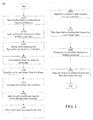
FIGS. 1 is a flow diagram of an example assembly process in accordance with the present disclosure; -
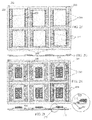
FIGS. 2A-2I are various views of matrix heat sink frame assembled with device die in accordance with the present disclosure; and -
FIGS. 3A-3B are views of an exposed heat sink HVQFN package assembled in accordance with the present disclosure. - While the invention is amenable to various modifications and alternative forms, specifics thereof have been shown by way of example in the drawings and will be described in detail. It should be understood, however, that the intention is not to limit the invention to the particular embodiments described. On the contrary, the intention is to cover all modifications, equivalents, and alternatives falling within the spirit and scope of the invention as defined by the appended claims.
- As the complexity of portable systems increases, there is a commensurate need to reduce the size of the individual components that make up the system; the system often is laid out on a printed circuit substrate. One way to reduce the size of individual components is through techniques that reduce the size of packages containing these devices. A package, often used, is the QFN (quad flat no-leads) package to reduce the vertical profile of the devices attached to the system printed circuit substrate. However, some applications may require that the QFN device handle sufficient power that may thermally stress the device die and packaging. Consequently, a heat sink is required to dissipate any excess heat; yet, the heat sink cannot add appreciably to the vertical profile. There is a need for a QFN or similar package that can accommodate a device die with a heat sink with an acceptable profile.
- The present disclosure has been found useful in enhancing the heat dissipation characteristics a power FET device assembled in a HVQFN package. These devices may be expected to dissipate about 100mW to about 5W, or more.
- Example devices may range in size from 3x3 mm up to 20x20 mm. A heat sink array would be a HVQFN strip size of about 70x250mm (or slight smaller so that it can be accommodated on the 200 mm sawing system.
- Thus, depending on heat sink size this tooling could hold something in the range of 50 (for larger package size) to 2500 for (smaller package size). The number of pins may range from minimal 3 pins (including the heat sink) to about 100, as in an example combining of a power device and controller in one package. The heat sink size will depend upon the power handling requirements of the particular device.
- In an example process the wafers are ground down to about 200 µm to prepare the device die that will ultimately be assembled onto the heat sink. To further reduce vertical profile, in another example process, the back grind thickness may be reduced down to 50 µm, after this process the back side metallization is applied. This metallization is in the order of a few micro-meters. One, or more metallization deposition techniques may be applied or even a combination of them (e.g., initial sputter layer which is increased in thickness by a plating process). The metallization provides a solderable surface on the die back side for optimal thermal (and electrical) contact of the die to the heat sink. Glue die bonding is possible also but will in general have a lower thermal contact.
- The present disclosure obviates the need to attach a separate heat sink to the QFN package in that the underside of the package is in direct contact with the PCB; the PCB provides a large area in which heat may be dissipated. Having prepared the underside of the devices, the attaching of the device die to the heat sink portion prior to assembly in a QFN lead frame, provides for better heat spreading that for a device die packaging in a conventional QFN configuration.
- Making reference to
FIG. 1 , in anexample process 100 according to the disclosure, a wafer substrate on its under-side undergoes back-grinding to aprescribed thickness 110. After back grinding, a suitable bondable conductive surface is applied to the wafer's under-side 115. The bondable conductive surface may be applied with a variety of techniques, which may include, but are not limited to, sputtering, evaporation, chemical vapor deposition, electro-plating, or a combination thereof. Bondable conductive surfaces may include NiAu, Cu, NiAg, or other suitable alloys. After the wafer under-side of the wafer is coated, the wafer is diced and device die, having bondable under-sides, are separated out 120. Dicing of the wafer may be accomplished with sawing, cleaving, laser ablation or other suitable method. - In another example process, the device die having a bondable underside surfaces may be prepared, in advance, in a separate process or from a third party. The prepared device die are bonded to the heat sink array, as described in the present disclosure.
- This bondable surface is only needed in case of soldering and when good electrical contact to the Si back side is needed. Alternatively for a glue die bonding a bondable back side in the form of metallization is acceptable, as long as a suitable thermal conductive glue is used with proper adhesion to the Si die.
- As determined by the device die type, a heat sink array is prepared 125. Having prepared the heat sink array, device die are bonded in die-attach areas on the
heat sink array 130. The device die, having solderable undersides, may be re-flow soldered onto the die attach areas of theheat sink array 125. In the present disclosure, heat sinks are arrayed in a heat sink frame (HS). The HS array permits the use of high-temperature die-bonding. The lead frame is spared from deleterious effects of the process temperatures, the effects including lead frame oxidation which may result in poor molding compound adhesion or wire-bonding problems. Also for HVQFN often mold tape is used during assembly; the mold tape cannot withstand temperature greater than 180 ° C for more than a few minutes. The user may make use of higher-temperature die-attach techniques which may include, but are not necessarily limited to, solder, eutectic, silver (Ag)-sinter, conductive adhesive, etc. For example, Ag-sinter is performed at about 200 °C to about 300°C, Pb-solder at about 350 °C, eutectic at about 400 °C, and conductive adhesive at 150 °C to 250 °C. - Further, the high temperatures may not be compatible with use of adhesive carrier tape; the high temperatures degrade the tape.
- The heat sink array with attached device die is placed on dicing foil and singulated (by sawing) into
individual assemblies 135. For the type of device die/heat sink assembly, a suitable lead frame array is selected 140. For example, an eight-pin device would require a lead frame of at least eight pad landings corresponding to each pin of the device, as well as contact areas for the heat sink attachment. Onto carrier tape, the lead frame array along with the device die/heat sink assemblies are placed 145. The device die/heat sink assembly is attached to alead frame 150. Mounting locations on the lead frame have glue or other attachment means to provide a bond to mounting tabs on the heat sink. - Devices are wire bonded to the bond pad areas on the
lead frame array 155. The array of device die/heat sink assemblies and the lead frame array are encapsulated in amolding compound 160.
In another example embodiment, the die/heat sink assembly might be attached to the mold tape alone (without connection to the lead frame bonding tabs). - After wire bonding and encapsulation, the carrier tape is removed. The assembled array of encapsulated devices is then sawed apart into individual assembled devices whose lead frame contacts are exposed, as well, as the exposed
heat sink 170; these exposed contact areas would be coplanar. The heat sink and exposed lead frame contacts would be prepared appropriately so that they have surfaces with a sufficient affinity to solder. - In another example embodiment, the use of wire bonds may not be appropriate, especially were minimizing interconnect inductance and/or resistance is critical. Ribbon bonding may often be used. For a given application, a wire bond may have a given diameter of about 25.4µm (.001 in) and a ribbon bond may have a cross-section of about 25.4µm x 76.2µm (.001 in x .003in). Interconnect inductance can cause impedance mismatches, ringing, distortion pulses. For high speed circuits, excess inductance results in reduced bandwidth. Because of this need for reduced inductance, ribbon bonding may often be specified instead of wire bonding. This is especially true for wide band components where parameters such as group delay must be controlled over a very wide bandwidth. Ribbon bonds may be preferred because a typical ribbon bond has two to three times less inductance than that of a wire bond. The increased cross-sectional area serves to lower the resistance of typical ribbon bonds compared to typical wire bonds, which in turn lowers RDSon in relevant electrical pathways. More detailed information may be found in "Quick Reference Guide: Ribbon Bond vs. Wire Bond." NATEL Engineering Co., Inc., Chatsworth, California, USA, pp.4.
- The device die/heat sink assemblies may be configured as strips, for example, 50mm x 150mm or 100mm x 300mm. Die sizes which may be used range from about 1mm x 1mm to about 20mm x 20mm. The number of device pins may range from 2 to 50 or more.
- In an example embodiment, as depicted in
FIGS. 2A-2I , a series of views illustrate the assembly of a device die according to the disclosure.FIGS. 2A-2B showheat sink array 200 in a frame. Although the figures illustrate an array of two rows and three columns, (for a total of six devices) such arrays used in IC device production may be hundreds of rows and columns of thousands of device positions.Individual heat sinks 210 with mountingtabs 230 are arrayed in aframe 220.FIGS. 2C-2D show device die 235 attached to each heat sink position. The device die 235 may be soldered (e.g., soft-soldered, eutectic soldered, or copper/tin soldered, etc.) or attached with conductive adhesive 215 to the heatsink array position 210. The heat sink array is roughly twice the thickness of an actual QFN lead frame and is half-etched on underside surfaces of connectingbars 220 and the underside surfaces 233 of the mountingtabs 230. In an example package, the heat sink is about 0.4mm thick and half-etched to about 0.2mm. After the device die 235 are mounted, theheat sink array 200 is mounted onto a dicingfoil 25 - Refer to
FIGS. 2E-2F . The half-etched areas of theheat sink array 200 are sawed to obtain individual device/heat sink assemblies 240. - Refer to
FIGS. 2F-2G . An examplelead frame assembly 205 has an array of six positions. Thelead frame assembly 205 is mounted onto a sawing/dicingtape 55. Connection bars 250 maintain the geometric relationships between thebond pads 255, so as to define device positions 245. Thebond pads 255 ultimately are the I/O terminals of the finished device. Four anchor pads 260 (which are selected from bond pads 255) in each device position 245 are prepared withspots 265 of glue or solder paste to attach the underside surfaces 233 the mountingtabs 230 of the device/heat sink assemblies 240. - Refer to
FIGS. 2H-2I . The individual device/heat sink assemblies 240 are mounted in each device position 245. The mountingtabs 230 are mounted to anchorpads 260. The magnifiedview 275 of the device mounting shows theanchor tab 260 upon which glue orsolder 265 is applied. The mountingtab 230 is anchored totab 260 with glue orsolder 265. Device die 235 is attached to theheat sink 210 with asolder type attachment 215. - The individual device/
heat sink assemblies 240 are wire bonded. The wire bonded devices are encapsulated in a molding compound. The lead frame connection bars 250 are removed during singulation. The underside surfaces ofbond pads 255,anchor pads 260, andheat sink 210 facilitate mounting of the device onto a system printed circuit board. - Refer to
FIGS. 3A-3B . In an example embodiment according to the present disclosure, in a lead frame array 300, aheat sink 310 atchosen locations 365, may be riveted or laser welded atanchor pads 360. - The number of fabricated devices can range from several hundred to even several thousand pieces. QFN package sizes may range from millimeters on a side down to about 0.5mm x 1mm. Other leadless (metal-based) packages may include, but are not necessarily limited to, aQFN (advanced quad flat no lead), LLGA (leadless land grid array), TLA (thermal leadless array), EFLGA (electroforming type land grid array), and TLEM (transcription lead of electroforming method), etc. The embodiments in the present disclosure may also be implemented in exposed-pad leaded devices such as HSOP (heat slug outline package), HQFP (heatsink quad flat pack) or other similar package types.
- Having been able to apply higher temperature processing to the die attach process in the die attaching of the device die onto the heat sink portion, a QFN device is assembled having a greater power dissipation performance and improved reliability. The die attach process occurs separately and thus, QFN lead frame or carrier is spared from the effects of the die attach process.
- Various exemplary embodiments are described in reference to specific illustrative examples. The illustrative examples are selected to assist a person of ordinary skill in the art to form a clear understanding of, and to practice the various embodiments. However, the scope of systems, structures and devices that may be constructed to have one or more of the embodiments, and the scope of methods that may be implemented according to one or more of the embodiments, are in no way confined to the specific illustrative examples that have been presented. On the contrary, as will be readily recognized by persons of ordinary skill in the relevant arts based on this description, many other configurations, arrangements, and methods according to the various embodiments may be implemented.
- To the extent positional designations such as top, bottom, upper, lower have been used in describing this disclosure, it will be appreciated that those designations are given with reference to the corresponding drawings, and that if the orientation of the device changes during manufacturing or operation, other positional relationships may apply instead. As described above, those positional relationships are described for clarity, not limitation.
- The present disclosure has been described with respect to particular embodiments and with reference to certain drawings, but the invention is not limited thereto, but rather, is set forth only by the claims. The drawings described are only schematic and are non-limiting. In the drawings, for illustrative purposes, the size of various elements may be exaggerated and not drawn to a particular scale. It is intended that this disclosure encompasses inconsequential variations in the relevant tolerances and properties of components and modes of operation thereof. Imperfect practice of the invention is intended to be covered.
- Where the term "comprising" is used in the present description and claims, it does not exclude other elements or steps. Where an indefinite or definite article is used when referring to a singular noun, e.g. "a" "an" or "the", this includes a plural of that noun unless something otherwise is specifically stated. Hence, the term "comprising" should not be interpreted as being restricted to the items listed thereafter; it does not exclude other elements or steps, and so the scope of the expression "a device comprising items A and B" should not be limited to devices consisting only of components A and B. This expression signifies that, with respect to the present disclosure, the only relevant components of the device are A and B.
- Numerous other embodiments of the disclosure will be apparent to persons skilled in the art without departing from the spirit and scope of the disclosure as defined in the appended claims.
Claims (14)
Applications Claiming Priority (1)
| Application Number | Priority Date | Filing Date | Title |
|---|---|---|---|
| US14/806,526 US9953903B2 (en) | 2015-07-22 | 2015-07-22 | Heatsink very-thin quad flat no-leads (HVQFN) package |
Publications (3)
| Publication Number | Publication Date |
|---|---|
| EP3121849A2 true EP3121849A2 (en) | 2017-01-25 |
| EP3121849A3 EP3121849A3 (en) | 2017-02-01 |
| EP3121849B1 EP3121849B1 (en) | 2019-10-23 |
Family
ID=56497641
Family Applications (1)
| Application Number | Title | Priority Date | Filing Date |
|---|---|---|---|
| EP16180307.7A Active EP3121849B1 (en) | 2015-07-22 | 2016-07-20 | Heatsink very-thin quad flat no-leads (hvqfn) package |
Country Status (3)
| Country | Link |
|---|---|
| US (1) | US9953903B2 (en) |
| EP (1) | EP3121849B1 (en) |
| CN (1) | CN106449435A (en) |
Cited By (1)
| Publication number | Priority date | Publication date | Assignee | Title |
|---|---|---|---|---|
| CN114883201A (en) * | 2022-05-20 | 2022-08-09 | 甬矽电子(宁波)股份有限公司 | AQFN production method |
Families Citing this family (4)
| Publication number | Priority date | Publication date | Assignee | Title |
|---|---|---|---|---|
| CN106920781A (en) * | 2015-12-28 | 2017-07-04 | 意法半导体有限公司 | Semiconductor package body and the method for forming semiconductor package body |
| JP6566927B2 (en) * | 2016-12-01 | 2019-08-28 | 三菱電機株式会社 | Semiconductor device and power conversion device |
| DE102017205813A1 (en) * | 2017-04-05 | 2018-10-11 | Mahle International Gmbh | A method of manufacturing a cooling device, a cooling device and a cooling arrangement |
| US10559545B2 (en) | 2017-10-04 | 2020-02-11 | Hand Held Products, Inc. | Land grid array patterns for modular electronics platforms and methods of performing the same |
Family Cites Families (8)
| Publication number | Priority date | Publication date | Assignee | Title |
|---|---|---|---|---|
| US5293301A (en) | 1990-11-30 | 1994-03-08 | Shinko Electric Industries Co., Ltd. | Semiconductor device and lead frame used therein |
| US5583377A (en) | 1992-07-15 | 1996-12-10 | Motorola, Inc. | Pad array semiconductor device having a heat sink with die receiving cavity |
| TW546806B (en) | 1999-11-08 | 2003-08-11 | Siliconware Precision Industries Co Ltd | Semiconductor package with common lead frame and heat sink |
| US6246111B1 (en) | 2000-01-25 | 2001-06-12 | Siliconware Precision Industries Co., Ltd. | Universal lead frame type of quad flat non-lead package of semiconductor |
| JP5155890B2 (en) * | 2008-06-12 | 2013-03-06 | ルネサスエレクトロニクス株式会社 | Semiconductor device and manufacturing method thereof |
| JP2012199436A (en) * | 2011-03-22 | 2012-10-18 | Toshiba Corp | Semiconductor device and manufacturing method of the same |
| CN102738024A (en) * | 2011-04-01 | 2012-10-17 | 飞思卡尔半导体公司 | Semiconductor packaging and lead frames thereof |
| CN102738022B (en) * | 2011-04-15 | 2017-05-17 | 飞思卡尔半导体公司 | Method for assembling semiconductor device containing insulating substrate and heat sink |
-
2015
- 2015-07-22 US US14/806,526 patent/US9953903B2/en not_active Expired - Fee Related
-
2016
- 2016-07-05 CN CN201610523344.XA patent/CN106449435A/en active Pending
- 2016-07-20 EP EP16180307.7A patent/EP3121849B1/en active Active
Non-Patent Citations (1)
| Title |
|---|
| None |
Cited By (1)
| Publication number | Priority date | Publication date | Assignee | Title |
|---|---|---|---|---|
| CN114883201A (en) * | 2022-05-20 | 2022-08-09 | 甬矽电子(宁波)股份有限公司 | AQFN production method |
Also Published As
| Publication number | Publication date |
|---|---|
| EP3121849A3 (en) | 2017-02-01 |
| CN106449435A (en) | 2017-02-22 |
| US20170025334A1 (en) | 2017-01-26 |
| US9953903B2 (en) | 2018-04-24 |
| EP3121849B1 (en) | 2019-10-23 |
Similar Documents
| Publication | Publication Date | Title |
|---|---|---|
| US20160005679A1 (en) | Exposed die quad flat no-leads (qfn) package | |
| US8513059B2 (en) | Pre-molded clip structure | |
| US20160005680A1 (en) | Exposed-Heatsink Quad Flat No-Leads (QFN) Package | |
| US9418919B2 (en) | Leadless chip carrier having improved mountability | |
| US11562949B2 (en) | Semiconductor package including undermounted die with exposed backside metal | |
| US9263375B2 (en) | System, method and apparatus for leadless surface mounted semiconductor package | |
| EP3121849B1 (en) | Heatsink very-thin quad flat no-leads (hvqfn) package | |
| US10658277B2 (en) | Semiconductor package with a heat spreader and method of manufacturing thereof | |
| US20090127677A1 (en) | Multi-Terminal Package Assembly For Semiconductor Devices | |
| US20160133617A1 (en) | Forming a panel of triple stack semiconductor packages | |
| US9355942B2 (en) | Gang clips having distributed-function tie bars | |
| US9263299B2 (en) | Exposed die clip bond power package | |
| US11721654B2 (en) | Ultra-thin multichip power devices | |
| US11984388B2 (en) | Semiconductor package structures and methods of manufacture | |
| US20170103939A1 (en) | Ultrathin routable quad flat no-leads (qfn) package | |
| EP3447795B1 (en) | Molded wafer level packaging method | |
| CN103681557B (en) | Semiconductor devices and its assemble method | |
| US9257374B1 (en) | Thin shrink outline package (TSOP) |
Legal Events
| Date | Code | Title | Description |
|---|---|---|---|
| PUAI | Public reference made under article 153(3) epc to a published international application that has entered the european phase |
Free format text: ORIGINAL CODE: 0009012 |
|
| STAA | Information on the status of an ep patent application or granted ep patent |
Free format text: STATUS: THE APPLICATION HAS BEEN PUBLISHED |
|
| PUAL | Search report despatched |
Free format text: ORIGINAL CODE: 0009013 |
|
| AK | Designated contracting states |
Kind code of ref document: A2 Designated state(s): AL AT BE BG CH CY CZ DE DK EE ES FI FR GB GR HR HU IE IS IT LI LT LU LV MC MK MT NL NO PL PT RO RS SE SI SK SM TR |
|
| AX | Request for extension of the european patent |
Extension state: BA ME |
|
| AK | Designated contracting states |
Kind code of ref document: A3 Designated state(s): AL AT BE BG CH CY CZ DE DK EE ES FI FR GB GR HR HU IE IS IT LI LT LU LV MC MK MT NL NO PL PT RO RS SE SI SK SM TR |
|
| AX | Request for extension of the european patent |
Extension state: BA ME |
|
| RIC1 | Information provided on ipc code assigned before grant |
Ipc: H01L 23/495 20060101ALI20161223BHEP Ipc: H01L 21/48 20060101ALI20161223BHEP Ipc: H01L 23/433 20060101AFI20161223BHEP |
|
| STAA | Information on the status of an ep patent application or granted ep patent |
Free format text: STATUS: REQUEST FOR EXAMINATION WAS MADE |
|
| 17P | Request for examination filed |
Effective date: 20170801 |
|
| RBV | Designated contracting states (corrected) |
Designated state(s): AL AT BE BG CH CY CZ DE DK EE ES FI FR GB GR HR HU IE IS IT LI LT LU LV MC MK MT NL NO PL PT RO RS SE SI SK SM TR |
|
| GRAP | Despatch of communication of intention to grant a patent |
Free format text: ORIGINAL CODE: EPIDOSNIGR1 |
|
| STAA | Information on the status of an ep patent application or granted ep patent |
Free format text: STATUS: GRANT OF PATENT IS INTENDED |
|
| INTG | Intention to grant announced |
Effective date: 20190607 |
|
| GRAJ | Information related to disapproval of communication of intention to grant by the applicant or resumption of examination proceedings by the epo deleted |
Free format text: ORIGINAL CODE: EPIDOSDIGR1 |
|
| STAA | Information on the status of an ep patent application or granted ep patent |
Free format text: STATUS: REQUEST FOR EXAMINATION WAS MADE |
|
| GRAP | Despatch of communication of intention to grant a patent |
Free format text: ORIGINAL CODE: EPIDOSNIGR1 |
|
| STAA | Information on the status of an ep patent application or granted ep patent |
Free format text: STATUS: GRANT OF PATENT IS INTENDED |
|
| GRAS | Grant fee paid |
Free format text: ORIGINAL CODE: EPIDOSNIGR3 |
|
| GRAA | (expected) grant |
Free format text: ORIGINAL CODE: 0009210 |
|
| STAA | Information on the status of an ep patent application or granted ep patent |
Free format text: STATUS: THE PATENT HAS BEEN GRANTED |
|
| INTC | Intention to grant announced (deleted) | ||
| INTG | Intention to grant announced |
Effective date: 20190902 |
|
| AK | Designated contracting states |
Kind code of ref document: B1 Designated state(s): AL AT BE BG CH CY CZ DE DK EE ES FI FR GB GR HR HU IE IS IT LI LT LU LV MC MK MT NL NO PL PT RO RS SE SI SK SM TR |
|
| REG | Reference to a national code |
Ref country code: GB Ref legal event code: FG4D |
|
| REG | Reference to a national code |
Ref country code: CH Ref legal event code: EP |
|
| REG | Reference to a national code |
Ref country code: IE Ref legal event code: FG4D |
|
| REG | Reference to a national code |
Ref country code: DE Ref legal event code: R096 Ref document number: 602016022802 Country of ref document: DE |
|
| REG | Reference to a national code |
Ref country code: AT Ref legal event code: REF Ref document number: 1194652 Country of ref document: AT Kind code of ref document: T Effective date: 20191115 |
|
| REG | Reference to a national code |
Ref country code: NL Ref legal event code: MP Effective date: 20191023 |
|
| REG | Reference to a national code |
Ref country code: LT Ref legal event code: MG4D |
|
| PG25 | Lapsed in a contracting state [announced via postgrant information from national office to epo] |
Ref country code: PT Free format text: LAPSE BECAUSE OF FAILURE TO SUBMIT A TRANSLATION OF THE DESCRIPTION OR TO PAY THE FEE WITHIN THE PRESCRIBED TIME-LIMIT Effective date: 20200224 Ref country code: BG Free format text: LAPSE BECAUSE OF FAILURE TO SUBMIT A TRANSLATION OF THE DESCRIPTION OR TO PAY THE FEE WITHIN THE PRESCRIBED TIME-LIMIT Effective date: 20200123 Ref country code: GR Free format text: LAPSE BECAUSE OF FAILURE TO SUBMIT A TRANSLATION OF THE DESCRIPTION OR TO PAY THE FEE WITHIN THE PRESCRIBED TIME-LIMIT Effective date: 20200124 Ref country code: FI Free format text: LAPSE BECAUSE OF FAILURE TO SUBMIT A TRANSLATION OF THE DESCRIPTION OR TO PAY THE FEE WITHIN THE PRESCRIBED TIME-LIMIT Effective date: 20191023 Ref country code: NO Free format text: LAPSE BECAUSE OF FAILURE TO SUBMIT A TRANSLATION OF THE DESCRIPTION OR TO PAY THE FEE WITHIN THE PRESCRIBED TIME-LIMIT Effective date: 20200123 Ref country code: SE Free format text: LAPSE BECAUSE OF FAILURE TO SUBMIT A TRANSLATION OF THE DESCRIPTION OR TO PAY THE FEE WITHIN THE PRESCRIBED TIME-LIMIT Effective date: 20191023 Ref country code: LV Free format text: LAPSE BECAUSE OF FAILURE TO SUBMIT A TRANSLATION OF THE DESCRIPTION OR TO PAY THE FEE WITHIN THE PRESCRIBED TIME-LIMIT Effective date: 20191023 Ref country code: NL Free format text: LAPSE BECAUSE OF FAILURE TO SUBMIT A TRANSLATION OF THE DESCRIPTION OR TO PAY THE FEE WITHIN THE PRESCRIBED TIME-LIMIT Effective date: 20191023 Ref country code: PL Free format text: LAPSE BECAUSE OF FAILURE TO SUBMIT A TRANSLATION OF THE DESCRIPTION OR TO PAY THE FEE WITHIN THE PRESCRIBED TIME-LIMIT Effective date: 20191023 Ref country code: LT Free format text: LAPSE BECAUSE OF FAILURE TO SUBMIT A TRANSLATION OF THE DESCRIPTION OR TO PAY THE FEE WITHIN THE PRESCRIBED TIME-LIMIT Effective date: 20191023 |
|
| PG25 | Lapsed in a contracting state [announced via postgrant information from national office to epo] |
Ref country code: RS Free format text: LAPSE BECAUSE OF FAILURE TO SUBMIT A TRANSLATION OF THE DESCRIPTION OR TO PAY THE FEE WITHIN THE PRESCRIBED TIME-LIMIT Effective date: 20191023 Ref country code: HR Free format text: LAPSE BECAUSE OF FAILURE TO SUBMIT A TRANSLATION OF THE DESCRIPTION OR TO PAY THE FEE WITHIN THE PRESCRIBED TIME-LIMIT Effective date: 20191023 Ref country code: IS Free format text: LAPSE BECAUSE OF FAILURE TO SUBMIT A TRANSLATION OF THE DESCRIPTION OR TO PAY THE FEE WITHIN THE PRESCRIBED TIME-LIMIT Effective date: 20200224 |
|
| PG25 | Lapsed in a contracting state [announced via postgrant information from national office to epo] |
Ref country code: AL Free format text: LAPSE BECAUSE OF FAILURE TO SUBMIT A TRANSLATION OF THE DESCRIPTION OR TO PAY THE FEE WITHIN THE PRESCRIBED TIME-LIMIT Effective date: 20191023 |
|
| REG | Reference to a national code |
Ref country code: DE Ref legal event code: R097 Ref document number: 602016022802 Country of ref document: DE |
|
| PG2D | Information on lapse in contracting state deleted |
Ref country code: IS |
|
| PG25 | Lapsed in a contracting state [announced via postgrant information from national office to epo] |
Ref country code: DK Free format text: LAPSE BECAUSE OF FAILURE TO SUBMIT A TRANSLATION OF THE DESCRIPTION OR TO PAY THE FEE WITHIN THE PRESCRIBED TIME-LIMIT Effective date: 20191023 Ref country code: EE Free format text: LAPSE BECAUSE OF FAILURE TO SUBMIT A TRANSLATION OF THE DESCRIPTION OR TO PAY THE FEE WITHIN THE PRESCRIBED TIME-LIMIT Effective date: 20191023 Ref country code: RO Free format text: LAPSE BECAUSE OF FAILURE TO SUBMIT A TRANSLATION OF THE DESCRIPTION OR TO PAY THE FEE WITHIN THE PRESCRIBED TIME-LIMIT Effective date: 20191023 Ref country code: CZ Free format text: LAPSE BECAUSE OF FAILURE TO SUBMIT A TRANSLATION OF THE DESCRIPTION OR TO PAY THE FEE WITHIN THE PRESCRIBED TIME-LIMIT Effective date: 20191023 Ref country code: ES Free format text: LAPSE BECAUSE OF FAILURE TO SUBMIT A TRANSLATION OF THE DESCRIPTION OR TO PAY THE FEE WITHIN THE PRESCRIBED TIME-LIMIT Effective date: 20191023 Ref country code: IS Free format text: LAPSE BECAUSE OF FAILURE TO SUBMIT A TRANSLATION OF THE DESCRIPTION OR TO PAY THE FEE WITHIN THE PRESCRIBED TIME-LIMIT Effective date: 20200223 |
|
| REG | Reference to a national code |
Ref country code: AT Ref legal event code: MK05 Ref document number: 1194652 Country of ref document: AT Kind code of ref document: T Effective date: 20191023 |
|
| PLBE | No opposition filed within time limit |
Free format text: ORIGINAL CODE: 0009261 |
|
| STAA | Information on the status of an ep patent application or granted ep patent |
Free format text: STATUS: NO OPPOSITION FILED WITHIN TIME LIMIT |
|
| PG25 | Lapsed in a contracting state [announced via postgrant information from national office to epo] |
Ref country code: SM Free format text: LAPSE BECAUSE OF FAILURE TO SUBMIT A TRANSLATION OF THE DESCRIPTION OR TO PAY THE FEE WITHIN THE PRESCRIBED TIME-LIMIT Effective date: 20191023 Ref country code: IT Free format text: LAPSE BECAUSE OF FAILURE TO SUBMIT A TRANSLATION OF THE DESCRIPTION OR TO PAY THE FEE WITHIN THE PRESCRIBED TIME-LIMIT Effective date: 20191023 Ref country code: SK Free format text: LAPSE BECAUSE OF FAILURE TO SUBMIT A TRANSLATION OF THE DESCRIPTION OR TO PAY THE FEE WITHIN THE PRESCRIBED TIME-LIMIT Effective date: 20191023 |
|
| 26N | No opposition filed |
Effective date: 20200724 |
|
| PG25 | Lapsed in a contracting state [announced via postgrant information from national office to epo] |
Ref country code: AT Free format text: LAPSE BECAUSE OF FAILURE TO SUBMIT A TRANSLATION OF THE DESCRIPTION OR TO PAY THE FEE WITHIN THE PRESCRIBED TIME-LIMIT Effective date: 20191023 Ref country code: SI Free format text: LAPSE BECAUSE OF FAILURE TO SUBMIT A TRANSLATION OF THE DESCRIPTION OR TO PAY THE FEE WITHIN THE PRESCRIBED TIME-LIMIT Effective date: 20191023 |
|
| PG25 | Lapsed in a contracting state [announced via postgrant information from national office to epo] |
Ref country code: MC Free format text: LAPSE BECAUSE OF FAILURE TO SUBMIT A TRANSLATION OF THE DESCRIPTION OR TO PAY THE FEE WITHIN THE PRESCRIBED TIME-LIMIT Effective date: 20191023 |
|
| REG | Reference to a national code |
Ref country code: CH Ref legal event code: PL |
|
| GBPC | Gb: european patent ceased through non-payment of renewal fee |
Effective date: 20200720 |
|
| REG | Reference to a national code |
Ref country code: BE Ref legal event code: MM Effective date: 20200731 |
|
| PG25 | Lapsed in a contracting state [announced via postgrant information from national office to epo] |
Ref country code: LU Free format text: LAPSE BECAUSE OF NON-PAYMENT OF DUE FEES Effective date: 20200720 Ref country code: LI Free format text: LAPSE BECAUSE OF NON-PAYMENT OF DUE FEES Effective date: 20200731 Ref country code: CH Free format text: LAPSE BECAUSE OF NON-PAYMENT OF DUE FEES Effective date: 20200731 Ref country code: FR Free format text: LAPSE BECAUSE OF NON-PAYMENT OF DUE FEES Effective date: 20200731 Ref country code: GB Free format text: LAPSE BECAUSE OF NON-PAYMENT OF DUE FEES Effective date: 20200720 |
|
| PG25 | Lapsed in a contracting state [announced via postgrant information from national office to epo] |
Ref country code: BE Free format text: LAPSE BECAUSE OF NON-PAYMENT OF DUE FEES Effective date: 20200731 |
|
| PG25 | Lapsed in a contracting state [announced via postgrant information from national office to epo] |
Ref country code: IE Free format text: LAPSE BECAUSE OF NON-PAYMENT OF DUE FEES Effective date: 20200720 |
|
| PG25 | Lapsed in a contracting state [announced via postgrant information from national office to epo] |
Ref country code: TR Free format text: LAPSE BECAUSE OF FAILURE TO SUBMIT A TRANSLATION OF THE DESCRIPTION OR TO PAY THE FEE WITHIN THE PRESCRIBED TIME-LIMIT Effective date: 20191023 Ref country code: MT Free format text: LAPSE BECAUSE OF FAILURE TO SUBMIT A TRANSLATION OF THE DESCRIPTION OR TO PAY THE FEE WITHIN THE PRESCRIBED TIME-LIMIT Effective date: 20191023 Ref country code: CY Free format text: LAPSE BECAUSE OF FAILURE TO SUBMIT A TRANSLATION OF THE DESCRIPTION OR TO PAY THE FEE WITHIN THE PRESCRIBED TIME-LIMIT Effective date: 20191023 |
|
| PG25 | Lapsed in a contracting state [announced via postgrant information from national office to epo] |
Ref country code: MK Free format text: LAPSE BECAUSE OF FAILURE TO SUBMIT A TRANSLATION OF THE DESCRIPTION OR TO PAY THE FEE WITHIN THE PRESCRIBED TIME-LIMIT Effective date: 20191023 |
|
| PGFP | Annual fee paid to national office [announced via postgrant information from national office to epo] |
Ref country code: DE Payment date: 20220621 Year of fee payment: 7 |
|
| REG | Reference to a national code |
Ref country code: DE Ref legal event code: R119 Ref document number: 602016022802 Country of ref document: DE |
|
| PG25 | Lapsed in a contracting state [announced via postgrant information from national office to epo] |
Ref country code: DE Free format text: LAPSE BECAUSE OF NON-PAYMENT OF DUE FEES Effective date: 20240201 |