EP3119926B1 - Multi-junction artificial photosynthetic cell with enhanced photovoltages - Google Patents
Multi-junction artificial photosynthetic cell with enhanced photovoltages Download PDFInfo
- Publication number
- EP3119926B1 EP3119926B1 EP15764783.5A EP15764783A EP3119926B1 EP 3119926 B1 EP3119926 B1 EP 3119926B1 EP 15764783 A EP15764783 A EP 15764783A EP 3119926 B1 EP3119926 B1 EP 3119926B1
- Authority
- EP
- European Patent Office
- Prior art keywords
- semiconductor layer
- section
- junction
- semiconductor
- layers
- Prior art date
- Legal status (The legal status is an assumption and is not a legal conclusion. Google has not performed a legal analysis and makes no representation as to the accuracy of the status listed.)
- Active
Links
Images




Classifications
-
- C—CHEMISTRY; METALLURGY
- C25—ELECTROLYTIC OR ELECTROPHORETIC PROCESSES; APPARATUS THEREFOR
- C25B—ELECTROLYTIC OR ELECTROPHORETIC PROCESSES FOR THE PRODUCTION OF COMPOUNDS OR NON-METALS; APPARATUS THEREFOR
- C25B1/00—Electrolytic production of inorganic compounds or non-metals
- C25B1/50—Processes
- C25B1/55—Photoelectrolysis
-
- C—CHEMISTRY; METALLURGY
- C25—ELECTROLYTIC OR ELECTROPHORETIC PROCESSES; APPARATUS THEREFOR
- C25B—ELECTROLYTIC OR ELECTROPHORETIC PROCESSES FOR THE PRODUCTION OF COMPOUNDS OR NON-METALS; APPARATUS THEREFOR
- C25B1/00—Electrolytic production of inorganic compounds or non-metals
- C25B1/01—Products
- C25B1/02—Hydrogen or oxygen
- C25B1/04—Hydrogen or oxygen by electrolysis of water
-
- C—CHEMISTRY; METALLURGY
- C25—ELECTROLYTIC OR ELECTROPHORETIC PROCESSES; APPARATUS THEREFOR
- C25B—ELECTROLYTIC OR ELECTROPHORETIC PROCESSES FOR THE PRODUCTION OF COMPOUNDS OR NON-METALS; APPARATUS THEREFOR
- C25B3/00—Electrolytic production of organic compounds
- C25B3/20—Processes
- C25B3/25—Reduction
-
- C—CHEMISTRY; METALLURGY
- C25—ELECTROLYTIC OR ELECTROPHORETIC PROCESSES; APPARATUS THEREFOR
- C25B—ELECTROLYTIC OR ELECTROPHORETIC PROCESSES FOR THE PRODUCTION OF COMPOUNDS OR NON-METALS; APPARATUS THEREFOR
- C25B3/00—Electrolytic production of organic compounds
- C25B3/20—Processes
- C25B3/25—Reduction
- C25B3/26—Reduction of carbon dioxide
-
- C—CHEMISTRY; METALLURGY
- C25—ELECTROLYTIC OR ELECTROPHORETIC PROCESSES; APPARATUS THEREFOR
- C25B—ELECTROLYTIC OR ELECTROPHORETIC PROCESSES FOR THE PRODUCTION OF COMPOUNDS OR NON-METALS; APPARATUS THEREFOR
- C25B9/00—Cells or assemblies of cells; Constructional parts of cells; Assemblies of constructional parts, e.g. electrode-diaphragm assemblies; Process-related cell features
-
- H—ELECTRICITY
- H01—ELECTRIC ELEMENTS
- H01G—CAPACITORS; CAPACITORS, RECTIFIERS, DETECTORS, SWITCHING DEVICES, LIGHT-SENSITIVE OR TEMPERATURE-SENSITIVE DEVICES OF THE ELECTROLYTIC TYPE
- H01G9/00—Electrolytic capacitors, rectifiers, detectors, switching devices, light-sensitive or temperature-sensitive devices; Processes of their manufacture
- H01G9/20—Light-sensitive devices
-
- H—ELECTRICITY
- H10—SEMICONDUCTOR DEVICES; ELECTRIC SOLID-STATE DEVICES NOT OTHERWISE PROVIDED FOR
- H10F—INORGANIC SEMICONDUCTOR DEVICES SENSITIVE TO INFRARED RADIATION, LIGHT, ELECTROMAGNETIC RADIATION OF SHORTER WAVELENGTH OR CORPUSCULAR RADIATION
- H10F10/00—Individual photovoltaic cells, e.g. solar cells
- H10F10/10—Individual photovoltaic cells, e.g. solar cells having potential barriers
- H10F10/16—Photovoltaic cells having only PN heterojunction potential barriers
- H10F10/161—Photovoltaic cells having only PN heterojunction potential barriers comprising multiple PN heterojunctions, e.g. tandem cells
-
- H—ELECTRICITY
- H10—SEMICONDUCTOR DEVICES; ELECTRIC SOLID-STATE DEVICES NOT OTHERWISE PROVIDED FOR
- H10F—INORGANIC SEMICONDUCTOR DEVICES SENSITIVE TO INFRARED RADIATION, LIGHT, ELECTROMAGNETIC RADIATION OF SHORTER WAVELENGTH OR CORPUSCULAR RADIATION
- H10F10/00—Individual photovoltaic cells, e.g. solar cells
- H10F10/10—Individual photovoltaic cells, e.g. solar cells having potential barriers
- H10F10/16—Photovoltaic cells having only PN heterojunction potential barriers
- H10F10/162—Photovoltaic cells having only PN heterojunction potential barriers comprising only Group II-VI materials, e.g. CdS/CdTe photovoltaic cells
-
- H—ELECTRICITY
- H10—SEMICONDUCTOR DEVICES; ELECTRIC SOLID-STATE DEVICES NOT OTHERWISE PROVIDED FOR
- H10F—INORGANIC SEMICONDUCTOR DEVICES SENSITIVE TO INFRARED RADIATION, LIGHT, ELECTROMAGNETIC RADIATION OF SHORTER WAVELENGTH OR CORPUSCULAR RADIATION
- H10F10/00—Individual photovoltaic cells, e.g. solar cells
- H10F10/10—Individual photovoltaic cells, e.g. solar cells having potential barriers
- H10F10/16—Photovoltaic cells having only PN heterojunction potential barriers
- H10F10/167—Photovoltaic cells having only PN heterojunction potential barriers comprising Group I-III-VI materials, e.g. CdS/CuInSe2 [CIS] heterojunction photovoltaic cells
-
- H—ELECTRICITY
- H10—SEMICONDUCTOR DEVICES; ELECTRIC SOLID-STATE DEVICES NOT OTHERWISE PROVIDED FOR
- H10F—INORGANIC SEMICONDUCTOR DEVICES SENSITIVE TO INFRARED RADIATION, LIGHT, ELECTROMAGNETIC RADIATION OF SHORTER WAVELENGTH OR CORPUSCULAR RADIATION
- H10F10/00—Individual photovoltaic cells, e.g. solar cells
- H10F10/10—Individual photovoltaic cells, e.g. solar cells having potential barriers
- H10F10/18—Photovoltaic cells having only Schottky potential barriers
-
- H—ELECTRICITY
- H10—SEMICONDUCTOR DEVICES; ELECTRIC SOLID-STATE DEVICES NOT OTHERWISE PROVIDED FOR
- H10F—INORGANIC SEMICONDUCTOR DEVICES SENSITIVE TO INFRARED RADIATION, LIGHT, ELECTROMAGNETIC RADIATION OF SHORTER WAVELENGTH OR CORPUSCULAR RADIATION
- H10F10/00—Individual photovoltaic cells, e.g. solar cells
- H10F10/10—Individual photovoltaic cells, e.g. solar cells having potential barriers
- H10F10/19—Photovoltaic cells having multiple potential barriers of different types, e.g. tandem cells having both PN and PIN junctions
-
- H—ELECTRICITY
- H10—SEMICONDUCTOR DEVICES; ELECTRIC SOLID-STATE DEVICES NOT OTHERWISE PROVIDED FOR
- H10F—INORGANIC SEMICONDUCTOR DEVICES SENSITIVE TO INFRARED RADIATION, LIGHT, ELECTROMAGNETIC RADIATION OF SHORTER WAVELENGTH OR CORPUSCULAR RADIATION
- H10F19/00—Integrated devices, or assemblies of multiple devices, comprising at least one photovoltaic cell covered by group H10F10/00, e.g. photovoltaic modules
- H10F19/40—Integrated devices, or assemblies of multiple devices, comprising at least one photovoltaic cell covered by group H10F10/00, e.g. photovoltaic modules comprising photovoltaic cells in a mechanically stacked configuration
-
- H—ELECTRICITY
- H10—SEMICONDUCTOR DEVICES; ELECTRIC SOLID-STATE DEVICES NOT OTHERWISE PROVIDED FOR
- H10F—INORGANIC SEMICONDUCTOR DEVICES SENSITIVE TO INFRARED RADIATION, LIGHT, ELECTROMAGNETIC RADIATION OF SHORTER WAVELENGTH OR CORPUSCULAR RADIATION
- H10F19/00—Integrated devices, or assemblies of multiple devices, comprising at least one photovoltaic cell covered by group H10F10/00, e.g. photovoltaic modules
- H10F19/80—Encapsulations or containers for integrated devices, or assemblies of multiple devices, having photovoltaic cells
- H10F19/804—Materials of encapsulations
-
- H—ELECTRICITY
- H10—SEMICONDUCTOR DEVICES; ELECTRIC SOLID-STATE DEVICES NOT OTHERWISE PROVIDED FOR
- H10F—INORGANIC SEMICONDUCTOR DEVICES SENSITIVE TO INFRARED RADIATION, LIGHT, ELECTROMAGNETIC RADIATION OF SHORTER WAVELENGTH OR CORPUSCULAR RADIATION
- H10F77/00—Constructional details of devices covered by this subclass
- H10F77/10—Semiconductor bodies
- H10F77/12—Active materials
-
- H—ELECTRICITY
- H10—SEMICONDUCTOR DEVICES; ELECTRIC SOLID-STATE DEVICES NOT OTHERWISE PROVIDED FOR
- H10F—INORGANIC SEMICONDUCTOR DEVICES SENSITIVE TO INFRARED RADIATION, LIGHT, ELECTROMAGNETIC RADIATION OF SHORTER WAVELENGTH OR CORPUSCULAR RADIATION
- H10F77/00—Constructional details of devices covered by this subclass
- H10F77/20—Electrodes
- H10F77/206—Electrodes for devices having potential barriers
- H10F77/211—Electrodes for devices having potential barriers for photovoltaic cells
-
- Y—GENERAL TAGGING OF NEW TECHNOLOGICAL DEVELOPMENTS; GENERAL TAGGING OF CROSS-SECTIONAL TECHNOLOGIES SPANNING OVER SEVERAL SECTIONS OF THE IPC; TECHNICAL SUBJECTS COVERED BY FORMER USPC CROSS-REFERENCE ART COLLECTIONS [XRACs] AND DIGESTS
- Y02—TECHNOLOGIES OR APPLICATIONS FOR MITIGATION OR ADAPTATION AGAINST CLIMATE CHANGE
- Y02E—REDUCTION OF GREENHOUSE GAS [GHG] EMISSIONS, RELATED TO ENERGY GENERATION, TRANSMISSION OR DISTRIBUTION
- Y02E10/00—Energy generation through renewable energy sources
- Y02E10/50—Photovoltaic [PV] energy
-
- Y—GENERAL TAGGING OF NEW TECHNOLOGICAL DEVELOPMENTS; GENERAL TAGGING OF CROSS-SECTIONAL TECHNOLOGIES SPANNING OVER SEVERAL SECTIONS OF THE IPC; TECHNICAL SUBJECTS COVERED BY FORMER USPC CROSS-REFERENCE ART COLLECTIONS [XRACs] AND DIGESTS
- Y02—TECHNOLOGIES OR APPLICATIONS FOR MITIGATION OR ADAPTATION AGAINST CLIMATE CHANGE
- Y02E—REDUCTION OF GREENHOUSE GAS [GHG] EMISSIONS, RELATED TO ENERGY GENERATION, TRANSMISSION OR DISTRIBUTION
- Y02E10/00—Energy generation through renewable energy sources
- Y02E10/50—Photovoltaic [PV] energy
- Y02E10/541—CuInSe2 material PV cells
-
- Y—GENERAL TAGGING OF NEW TECHNOLOGICAL DEVELOPMENTS; GENERAL TAGGING OF CROSS-SECTIONAL TECHNOLOGIES SPANNING OVER SEVERAL SECTIONS OF THE IPC; TECHNICAL SUBJECTS COVERED BY FORMER USPC CROSS-REFERENCE ART COLLECTIONS [XRACs] AND DIGESTS
- Y02—TECHNOLOGIES OR APPLICATIONS FOR MITIGATION OR ADAPTATION AGAINST CLIMATE CHANGE
- Y02E—REDUCTION OF GREENHOUSE GAS [GHG] EMISSIONS, RELATED TO ENERGY GENERATION, TRANSMISSION OR DISTRIBUTION
- Y02E10/00—Energy generation through renewable energy sources
- Y02E10/50—Photovoltaic [PV] energy
- Y02E10/543—Solar cells from Group II-VI materials
-
- Y—GENERAL TAGGING OF NEW TECHNOLOGICAL DEVELOPMENTS; GENERAL TAGGING OF CROSS-SECTIONAL TECHNOLOGIES SPANNING OVER SEVERAL SECTIONS OF THE IPC; TECHNICAL SUBJECTS COVERED BY FORMER USPC CROSS-REFERENCE ART COLLECTIONS [XRACs] AND DIGESTS
- Y02—TECHNOLOGIES OR APPLICATIONS FOR MITIGATION OR ADAPTATION AGAINST CLIMATE CHANGE
- Y02E—REDUCTION OF GREENHOUSE GAS [GHG] EMISSIONS, RELATED TO ENERGY GENERATION, TRANSMISSION OR DISTRIBUTION
- Y02E60/00—Enabling technologies; Technologies with a potential or indirect contribution to GHG emissions mitigation
- Y02E60/30—Hydrogen technology
- Y02E60/36—Hydrogen production from non-carbon containing sources, e.g. by water electrolysis
-
- Y—GENERAL TAGGING OF NEW TECHNOLOGICAL DEVELOPMENTS; GENERAL TAGGING OF CROSS-SECTIONAL TECHNOLOGIES SPANNING OVER SEVERAL SECTIONS OF THE IPC; TECHNICAL SUBJECTS COVERED BY FORMER USPC CROSS-REFERENCE ART COLLECTIONS [XRACs] AND DIGESTS
- Y02—TECHNOLOGIES OR APPLICATIONS FOR MITIGATION OR ADAPTATION AGAINST CLIMATE CHANGE
- Y02P—CLIMATE CHANGE MITIGATION TECHNOLOGIES IN THE PRODUCTION OR PROCESSING OF GOODS
- Y02P20/00—Technologies relating to chemical industry
- Y02P20/10—Process efficiency
- Y02P20/133—Renewable energy sources, e.g. sunlight
Definitions
- the semiconductor makes an ohmic contact with a metal on one side and a makes a Schottky contact with a metal an the other.
- Cu and Au were used as the ohmic and Schottky contacts for Cu 2 O, respectively, and Pt is used as the electrocatalyst on both sides.
- Each pore contains one section which is adjacent to the sections in the neighbouring pores.
- the active materials are electrodeposited in situ, using a conductive substrate functioning as a working electrode.
- the heterostructures are intended for photoelectrolysis when submerged in a feedstock in a bag-type reactor.
- US 4,094,751 discloses a tandem water splitting system consisting of two semiconductors which are physically adjacent to one another and electronically connected via their respective ohmic contacts.
- US 4,891,074 discloses a multi-junction solar cell consisting of several amorphous Si alloy semiconductor layers sandwiched between metal contacts, such that each adjacent semiconductor layer has an ohmic contact at the bottom, and a Schottky contact at the top. In another embodiment adjacent semiconductor layers are contacted with ohmic and Schottky layers, and separated by an insulator. The bandgaps of the adjacent semiconductors are matched.
- US 4,292,461 discloses a multi-junction tandem solar cell having a crystalline p-Si first semiconductor layer and an amorphous n-Si second semiconductor layer. Ohmic and Schottky layers contact the first semiconductor, while the second semiconductor is contacted by an ohmic layer and a Schottky layer. The contacts are either metallic or indium doped tin oxide which is quasi metallic.
- the embodiments disclosed herein provide sufficient free energy to split water and/or reduce CO 2 to fuels and chemicals in an efficient and stable manner.
- Certain embodiments include the use of low-cost synthetic techniques to obtain semiconductor materials with designed composition, size and shape control. Certain embodiments include semiconductor materials containing earth abundant elements. Certain embodiments include a nano porous aluminum oxide template to create fault-tolerant systems that defy photo-corrosion and other degradative effects of a harsh electrochemically active environment.
- Certain embodiments include a multi-junction artificial photosynthesis unit having a plurality of vertically stacked semiconductor layers formed within a protective structure (e.g., a porous aluminum oxide structure).
- the multi-junction photosynthesis unit also includes a plurality of metal layers, with one or more metal layers interstitially disposed between each semiconductor layer and configured to forma a Schottky barrier or an ohmic junction with a surface of an adjacent semiconductor layer.
- Certain embodiments include a multi-junction artificial photosynthesis unit having a plurality of semiconductor layers, with each successive semiconductor layer having a greater thickness than the preceding semiconductor layer, the photogenerated current density produced over each layer being substantially equal.
- Figure 2 illustrates an embodiment of a photoreactor system 200 formed as a reactor vessel 210 including a plurality of multi-junction photosynthetic units 220 suspended in an electrolyte 230.
- the multi-junction photosynthetic units 220 can be suspended in a suitable electrolyte 230 contained in a photoreactor vessel 210.
- the vessel 210 can be a low-cost flexible plastic bag.
- the feedstock can include chemical substances (e.g., organic molecules, inorganic molecules, celluloses, hydrocarbons, non-biocompatible pollutants, alcohols, ethanol, methanol, isopropyl alcohol, pesticides, glucose, phenols, carboxylic acids, cyanide, ammonia, acetic acid, dyes, surfactants, chlorophenols, anilines, oxalic acid, and tartaric acid).
- chemical substances e.g., organic molecules, inorganic molecules, celluloses, hydrocarbons, non-biocompatible pollutants, alcohols, ethanol, methanol, isopropyl alcohol, pesticides, glucose, phenols, carboxylic acids, cyanide, ammonia, acetic acid, dyes, surfactants, chlorophenols, anilines, oxalic acid, and tartaric acid).
- Figures 3A-3C illustrate a multi-junction photosynthetic unit 300 in various stages of formation.
- the foundation of these units 300 will be a visible light-absorbing semiconductor isolated from the supporting electrolyte by a protective structure 310.
- the multi-junction photosynthetic unit can include a protective structure 310 in which layers forming an active element 320 of the multi-junction photosynthetic unit may be added.
- the protective structure 310 is a porous oxide (e.g., porous anodic aluminum oxide) in which semiconductor materials, metal layers, and electrocatalyst layers may be added to form an active element 320 within the protective structure 310.
- layers of the active element 320 may be electrodeposited within the porous structure of the protective structure 310 in successive fashion to form the functioning multi-junction photosynthetic unit 300.
- the protective structure 310 advantageously protects the active element from photo-corrosion and other corrosive effects of the electrolytic environment.
- Figure 3B illustrates a porous protective structure 310 joined to a conducting substrate 312.
- the conducting substrate 312 is formed onto one face of the protective structure 310.
- the conducting substrate 312 may then function as the working electrode (electrode of study) for electrodeposition of further layers forming the active element 320.
- the further layering can include a deposited electrocatalytic layer, followed by deposition of one or plurality of semiconductor layers, followed by deposition of an interfacial tunnel junction layers to create Schottky or ohmic junctions and capping the entire structure with deposition of another electrocatalyst layer.
- Figure 3C illustrates an active element 320 including multiple layers 322 formed in this manner.
- FIG. 4 An exemplary development method 400 for preparing a functional multi-junction photosynthetic unit for solar fuel production is illustrated schematically in Figure 4 .
- the process begins by preparing a porous protective structure 410.
- this protective structure is formed from an aluminum oxide material.
- the process then deposits a conducting substrate 420 on one side or face of the porous protective structure.
- the conducting substrate may then function as the working electrode as the process deposits layers of the active element 430 within the protective structure.
- Multiple layers may then be deposited within the protective structure (e.g., via electrodeposition) in successive fashion to form the active element of the unit. For example, layering may proceed by depositing a light-absorbing semiconductor layer followed by one or more metal layers, followed by another light-absorbing semiconductor layer, and then followed by one or more additional metal layers.
- a user, computer, and/or machine may measure the photovoltage parameters 440 of the multi-junction unit, and based on the measured photovoltages, determine the sufficiency of the photovoltages 450 as to whether they are sufficient to drive the desired redox reactions. If the measured photovoltages are acceptable, the process will end 460. If the measured photovoltages are not acceptable, the process can deposit additional layers of the active element 430 within the protective structure until the desired photovoltages are realized. For example, in many embodiments, the desired photovoltage will be greater than or equal to about 1.2 volts. In other embodiments, greater photovoltages will be desired, such as from about 1.2 to about 1.6 volts, or from about 1.6 to about 2.0 volts, or from about 2.0 volts to about 2.5 volts or even greater than 2.5 volts.
- Figure 5 illustrates an embodiment of a multi-junction photosynthetic unit 500 including an active element 520 made from a plurality of vertically stacked semiconductor layers 522 (n-or p-type) of same or different materials having same or different thicknesses, a plurality of Schottky metal layers 526, each being disposed adjacent to a semiconductor layer 522 and each contacting a surface of the adjacent semiconductor layer 522 to form a Schottky barrier junction, and a plurality of ohmic metal layers 528, each being disposed adjacent to a semiconductor layer 522 and each contacting a surface of the adjacent semiconductor layer 522 to form an Ohmic contact junction.
- an active element 520 made from a plurality of vertically stacked semiconductor layers 522 (n-or p-type) of same or different materials having same or different thicknesses
- a plurality of Schottky metal layers 526 each being disposed adjacent to a semiconductor layer 522 and each contacting a surface of the adjacent semiconductor layer 522 to form a Schottky
- Figure 6 illustrates another embodiment of a multi-junction photosynthetic unit 600 including an active structure 620 having a first section 630 and a second section 640.
- the first section 630 is disposed in the unit 600 such that the first section 630 is the first section to receive light 670 incident upon the multi-junction unit 600.
- the first section 630 includes a first semiconductor layer having a first doping type (n- or p-type), having a first thickness, and producing a first photogenerated current output.
- the second section 640 is disposed adjacent the first section 630 and includes a second semiconductor layer being made of the same semiconductor composition as the first semiconductor layer, having the first doping type (n-or-p-type), and having a second thickness, where the second thickness is more than the first thickness, with the second thickness selected to produce a second photogenerated current output that is substantially equal to the first photogenerated current output.
- a second semiconductor layer being made of the same semiconductor composition as the first semiconductor layer, having the first doping type (n-or-p-type), and having a second thickness, where the second thickness is more than the first thickness, with the second thickness selected to produce a second photogenerated current output that is substantially equal to the first photogenerated current output.
- first section 630 and second section 640, and other lower sections 650 when included, can have Schottky and/or ohmic metal layers, with each Schottky metal layer forming a Schottky barrier with a surface of an adjacent semiconductor layer and each ohmic metal layer forming an ohmic contact with a surface of an adjacent semiconductor layer.
- the semiconducting material can be an electrodeposited cadmium telluride (CdTe) film/nanostructure, an electrodeposited copper indium di-selenide (CuInSe 2 ) film/nanostructure, an electrodeposited cadmium selenide (CdSe) film/nanostructure, an electrodeposited cadmium sulfide (CdS) film/nanostructure, or an electrodeposited copper oxide (Cu 2 O) film/nanostructure.
- CdTe electrodeposited cadmium telluride
- CuInSe 2 copper indium di-selenide
- CdSe electrodeposited cadmium selenide
- CdS electrodeposited cadmium sulfide
- Cu 2 O electrodeposited copper oxide
- the illustrated embodiment can also include an anode and cathode electro catalyst 680 capping one or more ends.
- the anode and cathode electro catalysts can be transition metals, noble metals, metal oxides, conducting polymers, perovskite and spinel type oxides, etc.
- the second section 740 is disposed adjacent to the first section 730 and includes a second semiconductor layer being made of a second semiconducting material (different from the composition of the first semiconductor layer), producing a second photogenerated current density that is substantially equal to the first photogenerated current density, and having a second energy bandgap that is less than the first energy bandgap.
- the embodiment illustrated in Figure 7 may also include one or more lower sections 750 adjacent to the second section 740, the lower section(s) 750 made of a plurality of lower semiconductor material systems (n-or-p-type) that are different from the first and second semiconductor layers, each successively lower one of the lower sections 750 having an energy bandgap lower than the one immediately above it, and each successively lower one of the lower sections having a photogenerated current density at least equal to the one immediately above it.
- the lower section(s) 750 made of a plurality of lower semiconductor material systems (n-or-p-type) that are different from the first and second semiconductor layers, each successively lower one of the lower sections 750 having an energy bandgap lower than the one immediately above it, and each successively lower one of the lower sections having a photogenerated current density at least equal to the one immediately above it.
- Figure 8 illustrates another embodiment of a multi-junction photosynthetic unit 800 including an active structure 820 having a first section 830 and a second section 840.
- the first section 830 is disposed in the unit 800 such that the first section 830 is the first section to receive light 870 incident upon the multi-junction unit 800.
- the first section 830 includes a first semiconductor layer made of a first semiconductor composition, having a first thickness and a first band gap energy, and producing a first photogenerated output.
- the second section 840 is disposed adjacent to the first section 830 and includes a second semiconductor layer being made of the same semiconductor composition as the first semiconductor layer, having a second thickness, and producing a second photogenerated current output that is substantially equal to the first photogenerated output.
- the illustrated embodiment also includes at least one additional section 850 that is of different semiconductor composition than the composition of the first semiconductor layer 830, and has a different band gap energy than the first band gap energy.
- first section 830, second section 840, and at least one additional section 850 can have Schottky and/or ohmic metal layers, with each Schottky metal layer forming a Schottky barrier with a surface of an adjacent semiconductor layer and each ohmic metal layer forming an ohmic contact with a surface of an adjacent semiconductor layer.
- Examples of the embodiment illustrated in Figure 8 include a 5-junction Cu 2 O/Cu 2 O/CdSe/CdSe/CdTe unit, a 6-junction Cu 2 O/Cu 2 O/CdSe/CdSe/CdTC/CuInSe 2 unit, and a 7-junction Cu 2 O/Cu 2 O/Cu 2 O/CdSe/CdSe/CdTe/CuInSe 2 unit.
Landscapes
- Chemical & Material Sciences (AREA)
- Engineering & Computer Science (AREA)
- Organic Chemistry (AREA)
- Chemical Kinetics & Catalysis (AREA)
- Electrochemistry (AREA)
- Materials Engineering (AREA)
- Metallurgy (AREA)
- Inorganic Chemistry (AREA)
- Power Engineering (AREA)
- Microelectronics & Electronic Packaging (AREA)
- Life Sciences & Earth Sciences (AREA)
- Sustainable Energy (AREA)
- Sustainable Development (AREA)
- Photovoltaic Devices (AREA)
- Electrolytic Production Of Non-Metals, Compounds, Apparatuses Therefor (AREA)
- Electrodes For Compound Or Non-Metal Manufacture (AREA)
Description
- This application claims the benefit of United States Provisional Application No.
61/968,598 filed March 21, 2014 14/659,243 filed March 16, 2015 - Disclosed herein are photoelectrocatalytic devices and methods, including multi-junction artificial photosynthetic components and methods of use and manufacture thereof.
- Development of an inexpensive solar fuel conversion process for the cleavage of water and CO2 reduction could potentially generate fuels or industrial chemicals with net zero carbon emissions. Based on the thermodynamic requirements alone, solar radiation with photon energies greater than 1.23 electron-volts is required to split water or to reduce CO2 to fuels. However, water oxidation at photo-anode is a kinetically sluggish process and likewise CO2 reduction at photo-cathode needs high overpotentials, resulting in actual energy requirements greater than 2.0 V. Therefore, using a single light absorber unit for water splitting or CO2 reduction requires a semiconductor with large band gap (Eg > 2.5 eV), limiting the exploitation of a substantial portion of the solar spectrum.
- Several strategies have been pursued to increase the obtainable phovoltages while maximizing sunlight absorption. One strategy is the use of multijunction/tandem photovoltaic designs to convert a large portion of the terrestrial solar spectrum into high free energy materials that can be used as fuels and chemicals. It has been estimated that these strategies are capable of achieving -18% solar-to-hydrogen conversion efficiencies. Rocheleau, R. & Miller, E. Energy Fuels 12, 3 (1998). Indeed, John Turner and his colleagues have already demonstrated a solar-to-H2 conversion efficiency of 12.4% using multi junction III-V semiconductors in 1990's. Khaselev, O. & Turner, J. Science 280, 425 (1998). However, the high costs and complexities associated with device fabrication using triple junction a-Si, (Weber, M. & Dignam, M. J. Electrochem. Soc. 131 (1984)), and III-V semiconductors have prevented from commercial realization. Moreover, their stable operation in harsh electrochemical conditions for long hours remains insufficient.
Syed Mubeen et al. ("Synthesis of Chemicals Using Solar Energy with Stable Photoelectrochemically Active Heterostructures", NANO LETTERS, 13 (2013), 2110-2115) discloses a photoelectrochemical hetero-structure consisting of a porous aluminium oxide protective host having a semiconductor layer capped with metal in each pore. For each system (CdSe and Cu2O), the semiconductor makes an ohmic contact with a metal on one side and a makes a Schottky contact with a metal an the other. Cu and Au were used as the ohmic and Schottky contacts for Cu2O, respectively, and Pt is used as the electrocatalyst on both sides. Each pore contains one section which is adjacent to the sections in the neighbouring pores. The active materials are electrodeposited in situ, using a conductive substrate functioning as a working electrode. The heterostructures are intended for photoelectrolysis when submerged in a feedstock in a bag-type reactor.
US 4,094,751 discloses a tandem water splitting system consisting of two semiconductors which are physically adjacent to one another and electronically connected via their respective ohmic contacts.
US 4,891,074 discloses a multi-junction solar cell consisting of several amorphous Si alloy semiconductor layers sandwiched between metal contacts, such that each adjacent semiconductor layer has an ohmic contact at the bottom, and a Schottky contact at the top. In another embodiment adjacent semiconductor layers are contacted with ohmic and Schottky layers, and separated by an insulator. The bandgaps of the adjacent semiconductors are matched.
US 4,292,461 discloses a multi-junction tandem solar cell having a crystalline p-Si first semiconductor layer and an amorphous n-Si second semiconductor layer. Ohmic and Schottky layers contact the first semiconductor, while the second semiconductor is contacted by an ohmic layer and a Schottky layer. The contacts are either metallic or indium doped tin oxide which is quasi metallic. - Accordingly, there has been and remains a need to find reliable photoelectrochemical devices and methods for novel, carbon-neutral energy cycles using only sunlight as the energy input for solar-driven production of fuels and chemicals. Such devices and methods should be able to provide sufficient photovoltages while maximizing sunlight absorption. In addition, such devices and methods should resist the corrosive effects of a harsh electrochemical environment.
- Disclosed herein are multi-junction artificial photosynthetic units with novel architecture from simple low-cost electrochemical approaches according to claim 1. The embodiments disclosed herein provide sufficient free energy to split water and/or reduce CO2 to fuels and chemicals in an efficient and stable manner.
- Certain embodiments include the use of low-cost synthetic techniques to obtain semiconductor materials with designed composition, size and shape control. Certain embodiments include semiconductor materials containing earth abundant elements. Certain embodiments include a nano porous aluminum oxide template to create fault-tolerant systems that defy photo-corrosion and other degradative effects of a harsh electrochemically active environment.
- Certain embodiments include methods of fabricating high efficiency low-cost multijunction photovoltaic devices using simple electrochemical routes to increase a photoelectrochemical cell's voltages for driving the desired electrochemical processes.
- The multi-junction artificial photosynthesis unit includes a protective structure and an active element formed within the protective structure, the active element including first and second semiconductor layers and one or more metal layers disposed between the semiconductor layers, each metal layer forming a Schottky barrier junction or an ohmic junction with a surface of an adjacent semiconductor layer.
- Certain embodiments include a multi-junction artificial photosynthesis unit having a plurality of vertically stacked semiconductor layers formed within a protective structure (e.g., a porous aluminum oxide structure). The multi-junction photosynthesis unit also includes a plurality of metal layers, with one or more metal layers interstitially disposed between each semiconductor layer and configured to forma a Schottky barrier or an ohmic junction with a surface of an adjacent semiconductor layer.
- Certain embodiments include a multi-junction artificial photosynthesis unit having a plurality of semiconductor layers, with each successive semiconductor layer having a greater thickness than the preceding semiconductor layer, the photogenerated current density produced over each layer being substantially equal.
- Certain embodiments include a multi-junction artificial photosynthesis unit having a plurality of semiconductor layers, with each successive semiconductor layer having a different composition and producing a successively smaller energy bandgap, the photogenerated current density produced over each layer being substantially equal.
- Certain embodiments of a multi-junction artificial photosynthesis unit include one or more oxidation/reduction electro catalysts capping the unit, an ion-selective membrane covering the electrocatalyst(s), and/or a protective layer that covers and protects the unit.
- To further clarify the above and other advantages and features of the present disclosure, a more particular description of the invention will be rendered by reference to specific embodiments thereof which are illustrated in the appended drawings. It is appreciated that these drawings depict only illustrated embodiments of the invention and are therefore not to be considered limiting of its scope. Embodiments of the invention will be described and explained with additional specificity and detail through the use of the accompanying drawings in which:
-
FIG. 1 illustrates an exemplary multi-junction photosynthetic unit showing photo-catalyzed oxidation and reduction reactions; -
FIG. 2 illustrates a photoreactor system including a plurality of multi-junction photosynthetic units suspended in an electrolyte; -
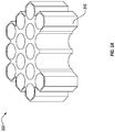
FIG. 3A illustrates a porous protective structure suitable for receiving layers of the multi-junction photosynthetic unit; -
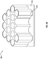
FIG. 3B illustrates a porous protective structure suitable for receiving layers of the multi-junction photosynthetic unit after deposition of a conducting backing layer; -
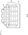
FIG. 3C illustrates an active element of multiple layers formed within a porous protective structure; -
FIG. 4 illustrates a method of preparing a multi-junction photosynthetic unit of the present disclosure for use in providing a desired redox reaction; -
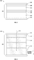
FIG. 5 illustrates an embodiment of a multi-junction photosynthetic unit having multiple layers; -
FIG. 6 illustrates an embodiment of a multi-junction photosynthetic unit having multiple layers with the same semiconductor material composition, with each successive semiconductor layer having a greater thickness than the preceding semiconductor layer; -
FIG. 7 illustrates an embodiment of a multi-junction photosynthetic unit having multiple layers of different semiconductor material composition, with each successive layer having a lower energy bandgap than the preceding layer; and -
FIG. 8 illustrates another embodiment of a multi-junction photosynthetic unit having multiple layers, with first and second semiconductor layers being formed of the same materials and having different thicknesses, and a third semiconductor layer being formed with materials different from the first and second semiconductor layers. - An exemplary multi-junction
photosynthetic unit 100 is shown inFigure 1 . The illustrated embodiment is a self-contained photocatalytic nanoreactor unit by which solar photons are transformed into electronic excitations which can be separated into electrons and holes which will move to the catalyst/electrolyte interface 110 of the structure and transfer to acceptor/donor surface species -
Figure 2 illustrates an embodiment of aphotoreactor system 200 formed as areactor vessel 210 including a plurality of multi-junctionphotosynthetic units 220 suspended in an electrolyte 230. When operating, the multi-junctionphotosynthetic units 220 can be suspended in a suitable electrolyte 230 contained in aphotoreactor vessel 210. In some embodiments, thevessel 210 can be a low-cost flexible plastic bag. - The electrolyte 230 can include a feedstock chemical, and the multi-junction photosynthetic unit(s) can be fully or partially submerged in the feedstock chemical. The feedstock can include water which on photo electro lysis produces H2 and O2. The feedstock can include at least one waste stream (e.g., from complex organic chemical industries, pharmaceutical processing, pesticide manufacturing, hydrocarbon refining, detergents, plastics, pulp and paper mills, textile dyes, agricultural, biofuels, chemical manufacturing, toxic hydrogen sulfide, hydrogen bromide, hydrogen chloride, municipal wastewater, iron and steel industry, coal plants, and tannery). The feedstock can include chemical substances (e.g., organic molecules, inorganic molecules, celluloses, hydrocarbons, non-biocompatible pollutants, alcohols, ethanol, methanol, isopropyl alcohol, pesticides, glucose, phenols, carboxylic acids, cyanide, ammonia, acetic acid, dyes, surfactants, chlorophenols, anilines, oxalic acid, and tartaric acid).
- Operation of such a photoreactor gives rise to oxidized reaction co-product(s). Such oxidized co-products can include chemical substance such as: biodegradable products produced from non-biodegradable organic waste streams, biocompatible organics which can be biologically treated in a downstream process, oxalic acid, halogens, bromine, sulfur, chlorine, and detoxified water. Hydrogen gas can react with carbon dioxide in this photosynthetic reactor to form one or more reduction products that include methane and water as co-products. In cases where water is a co-product, the water can be recycled back into the reaction mixture used to form hydrogen gas. Hydrogen gas can also react with carbon dioxide in this photosynthetic reactor to form methanol and water as co-products, or to form carbon monoxide and water as co-product.
-
Figures 3A-3C illustrate a multi-junctionphotosynthetic unit 300 in various stages of formation. The foundation of theseunits 300 will be a visible light-absorbing semiconductor isolated from the supporting electrolyte by aprotective structure 310. For example, the multi-junction photosynthetic unit can include aprotective structure 310 in which layers forming anactive element 320 of the multi-junction photosynthetic unit may be added. In some embodiments, theprotective structure 310 is a porous oxide (e.g., porous anodic aluminum oxide) in which semiconductor materials, metal layers, and electrocatalyst layers may be added to form anactive element 320 within theprotective structure 310. For example, layers of theactive element 320 may be electrodeposited within the porous structure of theprotective structure 310 in successive fashion to form the functioning multi-junctionphotosynthetic unit 300. Theprotective structure 310 advantageously protects the active element from photo-corrosion and other corrosive effects of the electrolytic environment. - The
protective structure 310 is a porous aluminum oxide. In other embodiments, theprotective structure 310 may be formed as track-etch polyester or polycarbonate (PC) templates, mesoporous silica and zeolite templates, and di-block co-polymeric templates. -
Figure 3B illustrates a porousprotective structure 310 joined to a conductingsubstrate 312. In the illustrated embodiment, the conductingsubstrate 312 is formed onto one face of theprotective structure 310. The conductingsubstrate 312 may then function as the working electrode (electrode of study) for electrodeposition of further layers forming theactive element 320. - For example, the further layering can include a deposited electrocatalytic layer, followed by deposition of one or plurality of semiconductor layers, followed by deposition of an interfacial tunnel junction layers to create Schottky or ohmic junctions and capping the entire structure with deposition of another electrocatalyst layer.
Figure 3C illustrates anactive element 320 including multiple layers 322 formed in this manner. - The conducting
substrate 312 may be formed from a metal or a conducting polymer. In preferred embodiments, the conductingsubstrate 312 is formed from 5d metals such as gold, platinum, and iridium. In preferred embodiments, the conductingsubstrate 312 is formed from 4d metals such as silver, palladium, rhodium, ruthenium, and molybdenum. In preferred embodiments, the conductingsubstrate 312 is formed from 3d metals such as titanium, iron, nickel, copper, cobalt, and manganese. The conductingsubstrate 312 may be formed using physical vapor deposition process such as electron beam deposition, sputter deposition, thermal evaporation, and pulsed laser deposition. The conductingsubstrate 312 may also be formed using chemical vapor deposition processes such as atomic layer chemical vapor deposition, plasma enhanced chemical vapor deposition, and microwave plasma-assisted deposition processes. - In other embodiments, an active element (such as illustrated active element 320) may be formed through a different process or combination of processes. For example, an active element 320 (or portions thereof) may be formed using electroless deposition, chemical/photochemical polymerization, sol-gel deposition, atmospheric pressure chemical vapor deposition, low-pressure chemical vapor deposition, highpressure chemical vapor deposition, vapor phase epitaxy and molecular bean epitaxy.
- An
exemplary development method 400 for preparing a functional multi-junction photosynthetic unit for solar fuel production is illustrated schematically inFigure 4 . As illustrated, the process begins by preparing a porous protective structure 410. In preferred embodiments, this protective structure is formed from an aluminum oxide material. The process then deposits a conductingsubstrate 420 on one side or face of the porous protective structure. The conducting substrate may then function as the working electrode as the process deposits layers of theactive element 430 within the protective structure. Multiple layers may then be deposited within the protective structure (e.g., via electrodeposition) in successive fashion to form the active element of the unit. For example, layering may proceed by depositing a light-absorbing semiconductor layer followed by one or more metal layers, followed by another light-absorbing semiconductor layer, and then followed by one or more additional metal layers. - After the formation of an active element, a user, computer, and/or machine may measure the photovoltage parameters 440 of the multi-junction unit, and based on the measured photovoltages, determine the sufficiency of the
photovoltages 450 as to whether they are sufficient to drive the desired redox reactions. If the measured photovoltages are acceptable, the process will end 460. If the measured photovoltages are not acceptable, the process can deposit additional layers of theactive element 430 within the protective structure until the desired photovoltages are realized. For example, in many embodiments, the desired photovoltage will be greater than or equal to about 1.2 volts. In other embodiments, greater photovoltages will be desired, such as from about 1.2 to about 1.6 volts, or from about 1.6 to about 2.0 volts, or from about 2.0 volts to about 2.5 volts or even greater than 2.5 volts. -
Figure 5 illustrates an embodiment of a multi-junctionphotosynthetic unit 500 including anactive element 520 made from a plurality of vertically stacked semiconductor layers 522 (n-or p-type) of same or different materials having same or different thicknesses, a plurality ofSchottky metal layers 526, each being disposed adjacent to asemiconductor layer 522 and each contacting a surface of theadjacent semiconductor layer 522 to form a Schottky barrier junction, and a plurality of ohmic metal layers 528, each being disposed adjacent to asemiconductor layer 522 and each contacting a surface of theadjacent semiconductor layer 522 to form an Ohmic contact junction. - For example, the
active element 520 may be formed with asemiconductor layer 522 as the bottom layer deposited adjacent to (or on top of) a conductingsubstrate 512. The layering of theactive element 520 can then include aSchottky metal layer 526 followed by anohmic metal layer 528 followed by anadditional semiconductor layer 522. In the illustrated embodiment, theactive element 520 is then layered with anotherSchottky metal layer 526. In some embodiments, the multi-junction photosynthetic unit can also include one or more oxidation/reduction electro catalysts capping the unit, an ion-selective membrane covering the electrocatalyst(s), and/or aprotective layer 560 that covers and protects the unit. -
Figure 6 illustrates another embodiment of a multi-junctionphotosynthetic unit 600 including anactive structure 620 having afirst section 630 and asecond section 640. Thefirst section 630 is disposed in theunit 600 such that thefirst section 630 is the first section to receive light 670 incident upon themulti-junction unit 600. Thefirst section 630 includes a first semiconductor layer having a first doping type (n- or p-type), having a first thickness, and producing a first photogenerated current output. Thesecond section 640 is disposed adjacent thefirst section 630 and includes a second semiconductor layer being made of the same semiconductor composition as the first semiconductor layer, having the first doping type (n-or-p-type), and having a second thickness, where the second thickness is more than the first thickness, with the second thickness selected to produce a second photogenerated current output that is substantially equal to the first photogenerated current output. - The embodiment illustrated in
Figure 6 may also include one or morelower sections 650 adjacent to thesecond section 640, the lower section(s) made of a plurality of lower band-gap semiconductor material systems that have the same composition and same doping type as the first and second semiconductor layers (n-or-p-type), each successively of higher thicknesses and having a photogenerated current density at least equal to the one immediately above it. - In addition, the
first section 630 andsecond section 640, and otherlower sections 650, when included, can have Schottky and/or ohmic metal layers, with each Schottky metal layer forming a Schottky barrier with a surface of an adjacent semiconductor layer and each ohmic metal layer forming an ohmic contact with a surface of an adjacent semiconductor layer. - In the illustrated embodiment, for example, the semiconducting material can be an electrodeposited cadmium telluride (CdTe) film/nanostructure, an electrodeposited copper indium di-selenide (CuInSe2) film/nanostructure, an electrodeposited cadmium selenide (CdSe) film/nanostructure, an electrodeposited cadmium sulfide (CdS) film/nanostructure, or an electrodeposited copper oxide (Cu2O) film/nanostructure.
- Metal layers forming ohmic junctions can be one or more metals selected from Group II B and Group III A of the periodic table (e.g., zinc, cadmium, mercury, boron, aluminum, gallium, and indium). Metal layers forming Schottky barrier junctions can be one or more metals selected from noble metal groups of the periodic table (e.g., platinum, palladium, rhodium, ruthenium, iridium, gold, silver, and copper).
- The illustrated embodiment can also include an anode and
cathode electro catalyst 680 capping one or more ends. The anode and cathode electro catalysts can be transition metals, noble metals, metal oxides, conducting polymers, perovskite and spinel type oxides, etc. -
Figure 7 illustrates another embodiment of a multi-junctionphotosynthetic unit 700 including anactive structure 720 having afirst section 730 and asecond section 740. Thefirst section 730 is disposed in theunit 700 such that thefirst section 730 is the first section to receive light 770 incident upon themulti-junction unit 700. Thefirst section 730 includes a first semiconductor layer (n-or-p-type), having a first thickness, having a first energy bandgap, and producing a first photogenerated current density. Thesecond section 740 is disposed adjacent to thefirst section 730 and includes a second semiconductor layer being made of a second semiconducting material (different from the composition of the first semiconductor layer), producing a second photogenerated current density that is substantially equal to the first photogenerated current density, and having a second energy bandgap that is less than the first energy bandgap. - The embodiment illustrated in
Figure 7 may also include one or morelower sections 750 adjacent to thesecond section 740, the lower section(s) 750 made of a plurality of lower semiconductor material systems (n-or-p-type) that are different from the first and second semiconductor layers, each successively lower one of thelower sections 750 having an energy bandgap lower than the one immediately above it, and each successively lower one of the lower sections having a photogenerated current density at least equal to the one immediately above it. - In addition, the
first section 730 andsecond section 740, and otherlower sections 750, when included, can have Schottky and/or ohmic metal layers, with each Schottky metal layer forming a Schottky barrier with a surface of an adjacent semiconductor layer and each ohmic metal layer forming an ohmic contact with a surface of an adjacent semiconductor layer. - In the illustrated embodiment, the first semiconductor layer of the
first section 730 can be formed from electrodeposited wide band gap metal oxides such as Cu2O, ZnO, TiO2, etc., and the second semiconductor layer of thesecond section 740 can be formed from electrodeposited CdSe, for example. The lower sections, when included, can include electrodeposited CdTe and CuInSe2, for example. Examples include a 3-junction Cu2O/CdSe/CdTe unit and a 4-junction Cu2O/CdSe/CdTe/CuInSe2 unit. -
Figure 8 illustrates another embodiment of a multi-junctionphotosynthetic unit 800 including anactive structure 820 having a first section 830 and a second section 840. The first section 830 is disposed in theunit 800 such that the first section 830 is the first section to receive light 870 incident upon themulti-junction unit 800. The first section 830 includes a first semiconductor layer made of a first semiconductor composition, having a first thickness and a first band gap energy, and producing a first photogenerated output. The second section 840 is disposed adjacent to the first section 830 and includes a second semiconductor layer being made of the same semiconductor composition as the first semiconductor layer, having a second thickness, and producing a second photogenerated current output that is substantially equal to the first photogenerated output. - The illustrated embodiment also includes at least one additional section 850 that is of different semiconductor composition than the composition of the first semiconductor layer 830, and has a different band gap energy than the first band gap energy.
- In addition, the first section 830, second section 840, and at least one additional section 850 can have Schottky and/or ohmic metal layers, with each Schottky metal layer forming a Schottky barrier with a surface of an adjacent semiconductor layer and each ohmic metal layer forming an ohmic contact with a surface of an adjacent semiconductor layer.
- Examples of the embodiment illustrated in
Figure 8 include a 5-junction Cu2O/Cu2O/CdSe/CdSe/CdTe unit, a 6-junction Cu2O/Cu2O/CdSe/CdSe/CdTC/CuInSe2 unit, and a 7-junction Cu2O/Cu2O/Cu2O/CdSe/CdSe/CdTe/CuInSe2 unit.
Claims (12)
- A multi-junction artificial photosynthesis unit comprising:
an active element, the active element comprising:a first section including a first semiconductor layer and one or more metal layers adjacent to the semiconductor layer;a second section adjacent to the first section and including a second semiconductor layer and one or more metal layers adjacent to the semiconductor layer;a protective structure, the protective structure being formed as a porous aluminum oxide material, the active element being formed within the protective structure,wherein the one or more metal layers of the first section and the one or more metal layers of the second section each form a Schottky barrier junction or an ohmic junction with a surface of an adjacent semiconductor layer, andwherein the one or more metal layers of the first section include a first Schottky metal layer and a first ohmic metal layer, the first Schottky metal layer being disposed on a surface of the first semiconductor layer opposite the second section and the first ohmic metal layer being disposed on a surface of the first semiconductor layer proximate to the second section, and wherein the one or more metal layers of the second section include a second Schottky metal layer disposed on a surface of the second semiconductor layer proximate to the first section, and wherein the second Schottky metal layer of the second section is adjacent to the first ohmic metal layer of the first section. - The multi-junction artificial photosynthesis unit of claim 1, further comprising a conducting substrate joined to one face of the protective structure, the conducting substrate functioning as a working electrode for further deposition of layers within the protective structure.
- The multi-junction artificial photosynthesis unit of claim 1 or claim 2, wherein the first semiconductor layer and the second semiconductor layer have the same composition, such as where the first and second semiconductor layers are formed from one or more of cadmium telluride (CdTe), copper indium di-selenide (CuInSe2), selenide (CdSe), cadmium sulfide (CdS), and copper oxide (Cu2O), and wherein the second semiconductor layer has a thickness that is greater than a thickness of the first semiconductor layer.
- The multi-junction artificial photosynthesis unit of claim 3, further comprising one or more lower sections each having a semiconductor layer of the same composition as the first and second semiconductor layers, each semiconductor layer of each lower section being of successively greater thickness as a distance from the first section increases.
- The multi-junction artificial photosynthesis unit of any one of claims 1 to 3, wherein at least one of the one or more metal layers of the first section or at least one of the one or more metal layers of the second section forms an ohmic junction with a surface of an adjacent semiconductor layer, and is formed from one or more of Group IIB and Group III A metals.
- The multi-junction artificial photosynthesis unit of any one of claims 1 to 5, wherein at least one of the one or more metal layers of the first section or at least one of the one or more metal layers of the second section forms a Schottky barrier junction with a surface of an adjacent semiconductor layer, and is formed from one or more noble metals.
- The multi-junction artificial photosynthesis unit of any one of claims 1 to 6, further comprising a first electrocatalyst cap on one end of the unit, and a second electrocatalyst cap on an opposite end of the unit, such as where the first and second electrocatalyst caps are formed from materials selected from the group consisting of transition metals, noble metals, metal oxides, conducting polymers, perovskite, and spinel type oxides.
- The multi-junction artificial photosynthesis unit of any one of claims 1 to 7, wherein the first semiconductor layer is formed of a first semiconductor material and has a first energy bandgap, and wherein the second semiconductor layer is formed of a second semiconductor material and has a second energy bandgap, the second energy bandgap being less than the first energy bandgap.
- The multi-junction artificial photosynthesis unit of claim 8, further comprising one or more lower sections, each lower section having a semiconductor layer formed of semiconductor materials different from the first and second semiconductor layers, each semiconductor layer of each lower section being of successively lower energy bandgap as a distance from the first section increases.
- The multi-junction artificial photosynthesis unit of claim 9, wherein the semiconductor layers of the one or more lower sections are formed from one or more of CdTe and CuInSe2 or wherein the first semiconductor layer is formed from one or more of Cu2O, ZnO, and TiO2, and wherein the second semiconductor layer is CdSe
- The multi-junction artificial photosynthesis unit of any one of claims 1 to 10, wherein the first semiconductor layer is formed of a first semiconductor material and has a first thickness and a first energy bandgap, and wherein the second semiconductor layer is formed of the first semiconductor material and has a second thickness, the second thickness being greater than the first thickness, the unit further comprising at least one additional lower semiconductor layer formed of a second semiconductor material and having an energy bandgap less than the first energy bandgap.
- A photoreactor system for producing solar fuel from redox reaction products, the photoreactor system comprising:a plurality of multi-junction artificial photosynthesis units as in any of the preceding claims;a vessel, the vessel containing the plurality of multi-junction artificial photosynthesis units; anda feedstock contained within the vessel, the plurality of multi-junction artificial photosynthetic units being fully or partially submerged within the feedstock.
Applications Claiming Priority (3)
| Application Number | Priority Date | Filing Date | Title |
|---|---|---|---|
| US201461968598P | 2014-03-21 | 2014-03-21 | |
| US14/659,243 US10100415B2 (en) | 2014-03-21 | 2015-03-16 | Multi-junction artificial photosynthetic cell with enhanced photovoltages |
| PCT/US2015/021059 WO2015142916A1 (en) | 2014-03-21 | 2015-03-17 | Multi-junction artificial photosynthetic cell with enhanced photovoltages |
Publications (3)
| Publication Number | Publication Date |
|---|---|
| EP3119926A1 EP3119926A1 (en) | 2017-01-25 |
| EP3119926A4 EP3119926A4 (en) | 2017-11-08 |
| EP3119926B1 true EP3119926B1 (en) | 2019-03-06 |
Family
ID=54145234
Family Applications (1)
| Application Number | Title | Priority Date | Filing Date |
|---|---|---|---|
| EP15764783.5A Active EP3119926B1 (en) | 2014-03-21 | 2015-03-17 | Multi-junction artificial photosynthetic cell with enhanced photovoltages |
Country Status (5)
| Country | Link |
|---|---|
| US (1) | US10100415B2 (en) |
| EP (1) | EP3119926B1 (en) |
| CN (1) | CN107075695B (en) |
| AU (1) | AU2015231504B2 (en) |
| WO (1) | WO2015142916A1 (en) |
Families Citing this family (3)
| Publication number | Priority date | Publication date | Assignee | Title |
|---|---|---|---|---|
| WO2018058094A1 (en) | 2016-09-26 | 2018-03-29 | University Of Iowa Research Foundation | Integrated membrane solar fuel production assembly |
| JP7362317B2 (en) * | 2019-07-02 | 2023-10-17 | 株式会社東芝 | Solar cells, laminates, multijunction solar cells, solar cell modules, and solar power generation systems |
| CN111334812B (en) * | 2020-03-05 | 2021-06-08 | 桂林电子科技大学 | Amorphous silicon thin film photoelectrode based on hydrated iron oxyhydroxide and preparation method thereof |
Family Cites Families (98)
| Publication number | Priority date | Publication date | Assignee | Title |
|---|---|---|---|---|
| DE2300273C3 (en) | 1972-01-07 | 1982-05-06 | Toray Industries, Inc., Tokyo | Device for wastewater treatment |
| CA1031296A (en) | 1973-11-19 | 1978-05-16 | Texas Gas Transmission Corporation | Multi-step chemical and radiation process for the production of gas |
| US3925212A (en) | 1974-01-02 | 1975-12-09 | Dimiter I Tchernev | Device for solar energy conversion by photo-electrolytic decomposition of water |
| US3998659A (en) | 1974-01-28 | 1976-12-21 | Texas Instruments Incorporated | Solar cell with semiconductor particles and method of fabrication |
| JPS5328751B2 (en) | 1974-11-27 | 1978-08-16 | ||
| US4021323A (en) | 1975-07-28 | 1977-05-03 | Texas Instruments Incorporated | Solar energy conversion |
| US4175016A (en) | 1975-09-02 | 1979-11-20 | Texas Gas Transmission Corporation | Radiolytic-chemical method for production of gases |
| US4011149A (en) | 1975-11-17 | 1977-03-08 | Allied Chemical Corporation | Photoelectrolysis of water by solar radiation |
| US4069120A (en) | 1976-09-21 | 1978-01-17 | United Technologies Corporation | Photo-electrolytic production of hydrogen |
| US4094751A (en) | 1976-09-30 | 1978-06-13 | Allied Chemical Corporation | Photochemical diodes |
| US4173494A (en) | 1977-02-14 | 1979-11-06 | Jack S. Kilby | Glass support light energy converter |
| US4270263A (en) | 1977-02-14 | 1981-06-02 | Texas Instruments Incorporated | Glass support light energy converter |
| US4203814A (en) | 1978-11-01 | 1980-05-20 | United Technologies Corporation | Hydrogen gas generation utilizing a bromide electrolyte and radiant energy |
| US4215182A (en) | 1979-05-29 | 1980-07-29 | Institute Of Gas Technology | Conversion of solar energy to chemical and electrical energy |
| IL58747A (en) | 1979-11-20 | 1982-11-30 | Yeda Res & Dev | Photoelectrochemical cell assembly having electrolyte contacts between semiconductor surfaces |
| US4236984A (en) | 1979-11-21 | 1980-12-02 | United Technologies Corporation | Hydrogen gas generation utilizing a bromide electrolyte, an amorphous silicon semiconductor and radiant energy |
| US4357400A (en) | 1979-12-11 | 1982-11-02 | Electric Power Research Institute, Inc. | Photoelectrochemical cell employing discrete semiconductor bodies |
| US4263110A (en) | 1979-12-17 | 1981-04-21 | United Technologies Corporation | Hydrogen-bromine generation utilizing semiconducting platelets suspended in a vertically flowing electrolyte solution |
| US4263111A (en) | 1979-12-17 | 1981-04-21 | United Technologies Corporation | Hydrogen generation utilizing semiconducting platelets suspended in a divergent vertically flowing electrolyte solution |
| US4381233A (en) | 1980-05-19 | 1983-04-26 | Asahi Kasei Kogyo Kabushiki Kaisha | Photoelectrolyzer |
| US4292461A (en) * | 1980-06-20 | 1981-09-29 | International Business Machines Corporation | Amorphous-crystalline tandem solar cell |
| US4891074A (en) * | 1980-11-13 | 1990-01-02 | Energy Conversion Devices, Inc. | Multiple cell photoresponsive amorphous alloys and devices |
| CH644471A5 (en) | 1981-02-02 | 1984-07-31 | Michael Graetzel | PRODUCT FOR USE AS A PHOTOCATALYST, PROCESS FOR PREPARING THE SAME AND USE OF THE SAME. |
| US4484992A (en) | 1981-02-04 | 1984-11-27 | Ciba-Geigy Corporation | Process for the production of hydrogen by means of heterogeneous photoredox catalysis |
| US4419278A (en) | 1981-05-04 | 1983-12-06 | Diamond Shamrock Corporation | Photoactive semiconductor material using true solid/solid solution mixed metal oxide |
| US4437954A (en) | 1981-06-19 | 1984-03-20 | Institute Of Gas Technology | Fuels production by photoelectrolysis of water and photooxidation of soluble biomass materials |
| JPS58166680A (en) | 1982-03-29 | 1983-10-01 | Semiconductor Energy Lab Co Ltd | Semiconductor device |
| FR2529379A1 (en) | 1982-06-28 | 1983-12-30 | Centre Nat Rech Scient | PHOTOSENSITIVE CELL FOR DECOMPOSITION OF WATER |
| US4533608A (en) | 1982-09-09 | 1985-08-06 | The Regents Of The University Of California | Electrolytic photodissociation of chemical compounds by iron oxide photochemical diodes |
| US4466869A (en) | 1983-08-15 | 1984-08-21 | Energy Conversion Devices, Inc. | Photolytic production of hydrogen |
| US4722776A (en) | 1984-03-14 | 1988-02-02 | The Texas A&M University System | One-unit photo-activated electrolyzer |
| US4643817A (en) | 1985-06-07 | 1987-02-17 | Electric Power Research Institute, Inc. | Photocell device for evolving hydrogen and oxygen from water |
| US4889604A (en) | 1987-08-06 | 1989-12-26 | Council Of Scientific & Industrial Research | Process for the photocatalytic decomposition of water into hydrogen and oxygen |
| US5116582A (en) | 1990-04-26 | 1992-05-26 | Photo-Catalytics, Inc. | Photocatalytic slurry reactor having turbulence generating means |
| US5118422A (en) | 1990-07-24 | 1992-06-02 | Photo-Catalytics, Inc. | Photocatalytic treatment of water |
| JPH075281B2 (en) | 1991-08-20 | 1995-01-25 | 工業技術院長 | Method for producing hydrogen and oxygen from water by metal-supported semiconductor photocatalyst using highly concentrated carbonate aqueous solution |
| JP2889778B2 (en) | 1992-11-20 | 1999-05-10 | 工業技術院長 | Water purification law |
| KR0130515B1 (en) | 1994-08-30 | 1998-04-03 | 강박광 | Novel photocatalyst and its production method and hydrogen production method using the same |
| US5581091A (en) | 1994-12-01 | 1996-12-03 | Moskovits; Martin | Nanoelectric devices |
| KR0180606B1 (en) | 1995-09-18 | 1999-03-20 | 강박광 | Novel photocatalyst and its production method and hydrogen production method using the same |
| KR100202238B1 (en) | 1996-10-07 | 1999-06-15 | 이서봉 | Novel zns photocatalyst, method thereof and production of hydrogen gas |
| DE69637769D1 (en) | 1996-10-09 | 2009-01-15 | Josuke Nakata | SEMICONDUCTOR DEVICE |
| US6361660B1 (en) | 1997-07-31 | 2002-03-26 | Avery N. Goldstein | Photoelectrochemical device containing a quantum confined group IV semiconductor nanoparticle |
| US6060026A (en) | 1997-07-31 | 2000-05-09 | Starfire Electronic Development & Mktg., Ltd. | Photoelectrochemical device containing a quantum confined silicon particle |
| DE69725601T2 (en) | 1997-08-27 | 2004-04-15 | Nakata, Josuke, Joyo | SPHERICAL SEMICONDUCTOR ARRANGEMENT, METHOD FOR THE PRODUCTION THEREOF, AND SPHERICAL SEMICONDUCTOR ARRANGEMENT MATERIAL |
| US20020096479A1 (en) | 2000-06-02 | 2002-07-25 | Butters Brian E. | System and method for photocatalytic treatment of contaminated media |
| CA2268469C (en) | 1998-04-10 | 2004-03-23 | University Of Central Florida | Apparatus and method for photocatalytic and thermocatalytic pollution control |
| KR100304349B1 (en) | 1998-09-09 | 2001-11-30 | 김충섭 | Photocatalyst for generating cadmium sulfide hydrogen and its production method and hydrogen production method using the same |
| KR100342856B1 (en) | 2000-02-22 | 2002-07-02 | 김충섭 | CdZnMS photocatalyst added with cation for water decomposition and preparation there for and method for producing hydrogen by use of the same |
| US6297190B1 (en) | 2000-02-23 | 2001-10-02 | Korea Research Institute Of Chemical Technology | ZnS photocatalyst, preparation therefor and method for producing hydrogen by use of the same |
| US6683023B2 (en) | 2000-04-21 | 2004-01-27 | Showa Denko K.K. | Photocatalytic powder and polymer composition |
| DE50007781D1 (en) | 2000-06-10 | 2004-10-21 | Degussa | Photocatalytic process |
| EP1175938A1 (en) | 2000-07-29 | 2002-01-30 | The Hydrogen Solar Production Company Limited | Photocatalytic film of iron oxide, electrode with such a photocatalytic film, method of producing such films, photoelectrochemical cell with the electrode and photoelectrochemical system with the cell, for the cleavage of water into hydrogen and oxygen |
| JP4107792B2 (en) | 2000-08-28 | 2008-06-25 | 独立行政法人科学技術振興機構 | Photocatalyst composed of metal oxynitride having visible light response |
| EP1255303B1 (en) | 2000-10-20 | 2016-06-29 | Sphelar Power Corporation | Light-emitting or light-detecting semiconductor module and method of manufacture thereof |
| US6827911B1 (en) | 2000-11-08 | 2004-12-07 | Bechtel Bwxt Idaho, Llc | Photoreactor with self-contained photocatalyst recapture |
| US6887816B2 (en) | 2000-12-28 | 2005-05-03 | Showa Denko K.K. | Photocatalyst |
| JP4064065B2 (en) | 2001-02-07 | 2008-03-19 | 独立行政法人科学技術振興機構 | Photocatalyst for visible light decomposition of water |
| JP4107807B2 (en) | 2001-02-07 | 2008-06-25 | 独立行政法人科学技術振興機構 | Oxysulfide photocatalyst for visible light decomposition of water |
| US20020187082A1 (en) | 2001-06-06 | 2002-12-12 | Chang-Yu Wu | Photocatalyst coated magnetic composite particle |
| JP3742873B2 (en) | 2001-07-10 | 2006-02-08 | 独立行政法人産業技術総合研究所 | Photocatalyst, method for producing hydrogen using the same, and method for decomposing toxic substances |
| US7956349B2 (en) * | 2001-12-05 | 2011-06-07 | Semiconductor Energy Laboratory Co., Ltd. | Organic semiconductor element |
| US7318915B2 (en) | 2002-01-25 | 2008-01-15 | United States Of America As Represented By The Administrator Of The National Aeronautics And Space Administration | Oxidation-reduction catalyst and its process of use |
| JP4113361B2 (en) | 2002-02-05 | 2008-07-09 | 日立ソフトウエアエンジニアリング株式会社 | Method for producing multilayer semiconductor nanoparticles |
| JP2003265962A (en) | 2002-03-18 | 2003-09-24 | Nittetsu Mining Co Ltd | Photocatalyst and method for producing the same |
| DE10216477B4 (en) | 2002-04-13 | 2006-01-19 | Liedy, Werner, Prof. Dr.-Ing. | New reactor and process concepts for the technical application of photocatalysis |
| JP4357801B2 (en) | 2002-06-25 | 2009-11-04 | 日鉄鉱業株式会社 | Highly active photocatalyst and method for producing the same |
| US7534488B2 (en) | 2003-09-10 | 2009-05-19 | The Regents Of The University Of California | Graded core/shell semiconductor nanorods and nanorod barcodes |
| US7193098B1 (en) | 2003-03-20 | 2007-03-20 | The Research Foundation Of State University Of New York | Process for producing semiconductor nanocrystal cores, core-shell, core-buffer-shell, and multiple layer systems in a non-coordinating solvent utilizing in situ surfactant generation |
| WO2004085306A1 (en) | 2003-03-26 | 2004-10-07 | Matsushita Electric Industrial Co. Ltd. | Apparatus for photolysis of water and method for photolysis of water |
| US7052587B2 (en) * | 2003-06-27 | 2006-05-30 | General Motors Corporation | Photoelectrochemical device and electrode |
| US7459065B2 (en) | 2004-02-18 | 2008-12-02 | General Motors Corporation | Hydrogen generator photovoltaic electrolysis reactor system |
| US7422696B2 (en) | 2004-02-20 | 2008-09-09 | Northwestern University | Multicomponent nanorods |
| JP2006068577A (en) | 2004-08-31 | 2006-03-16 | Sasano Densen Kk | Photocatalyst granules |
| TWI251271B (en) | 2004-09-22 | 2006-03-11 | Ind Tech Res Inst | Method for preparation of photocatalyst nanoparticles |
| JP4295231B2 (en) | 2005-03-01 | 2009-07-15 | 富士通株式会社 | Broadband light-absorbing photocatalyst and method for producing the same, and broadband light-absorbing photocatalyst-containing composition and molded article |
| CN101512003A (en) | 2005-05-16 | 2009-08-19 | 蒙大拿州立大学 | Composite nanomaterials for photocatalytic hydrogen production and methods of their use |
| US7625835B2 (en) | 2005-06-10 | 2009-12-01 | Gm Global Technology Operations, Inc. | Photocatalyst and use thereof |
| US7230269B2 (en) * | 2005-06-13 | 2007-06-12 | The Trustees Of Princeton University | Organic photosensitive cells having a reciprocal-carrier exciton blocking layer |
| US7763149B2 (en) | 2005-08-19 | 2010-07-27 | North Carolina State University | Solar photocatalysis using transition-metal oxides combining d0 and d6 electron configurations |
| US7820022B2 (en) | 2005-11-28 | 2010-10-26 | General Electric Company | Photoelectrochemical cell and method of manufacture |
| TWI280893B (en) | 2005-12-23 | 2007-05-11 | Ind Tech Res Inst | Nano photocatalytic solution and application thereof |
| TW200732036A (en) | 2006-02-01 | 2007-09-01 | Toshiba Lighting & Technology | Photocatalysis material, photocatalysis body, photocatalysis product, luminaire and manufacturing method thereof |
| GB0621246D0 (en) | 2006-10-25 | 2006-12-06 | Uvps Environmental Solutions L | Photocatalytic reactor |
| JP2010519057A (en) | 2007-02-20 | 2010-06-03 | イッサム リサーチ ディベロップメント カンパニー オブ ザ ヘブライ ユニバーシティー オブ エルサレム,リミテッド | Hybrid metal semiconductor nanoparticles, photoinduced charge separation methods and applications |
| US8003563B2 (en) | 2007-03-23 | 2011-08-23 | Kabushiki Kaisha Toshiba | Method for producing tungsten trioxide powder for photocatalyst, tungsten trioxide powder for photocatalyst, and photocatalyst product |
| DE102007028391A1 (en) | 2007-06-15 | 2008-12-18 | Nano-X Gmbh | Particles or coating for splitting water |
| US9181555B2 (en) | 2007-07-23 | 2015-11-10 | Ramot At Tel-Aviv University Ltd. | Photocatalytic hydrogen production and polypeptides capable of same |
| CN101795767B (en) | 2007-09-05 | 2012-07-04 | 株式会社东芝 | Visible light-responsive photocatalyst powder, visible light-responsive photocatalyst material, photocatalyst coating, and photocatalyst product using the same |
| TW200925116A (en) | 2007-12-05 | 2009-06-16 | Ind Tech Res Inst | Photocatalytic reaction system for water purification |
| KR100945035B1 (en) | 2008-01-29 | 2010-03-05 | 재단법인서울대학교산학협력재단 | Visible Light Responsive Photocatalyst Composition Using Tungsten Oxide and Manufacturing Method Thereof |
| ITSA20080012A1 (en) | 2008-05-29 | 2009-11-30 | Univ Degli Studi Salerno | CATALYTIC PHOTOREACTOR WITH HIGH LIGHT EFFICIENCY FOR INTENSIFIED PHOTOSSIDATION PROCESSES |
| EP2294002A4 (en) | 2008-06-25 | 2012-12-26 | Hydrogen Generation Inc | IMPROVED PROCESS FOR HYDROGEN PRODUCTION |
| KR20110042271A (en) * | 2008-07-03 | 2011-04-26 | 아이엠이씨 | Multi-junction photovoltaic modules and processing methods thereof |
| US20100176067A1 (en) | 2008-10-31 | 2010-07-15 | Boyd Joel E | Photocatalytic reactor and process for photocatalysis |
| JP2011036770A (en) | 2009-08-07 | 2011-02-24 | Hokkaido Univ | Method for producing noble metal-supported photocatalyst particle |
| JP2011224534A (en) | 2009-09-16 | 2011-11-10 | Sumitomo Chemical Co Ltd | Photocatalyst composite and photocatalyst functional product using the same |
| KR101003808B1 (en) * | 2010-04-06 | 2010-12-23 | 한국기계연구원 | Multiple solar cell with PUN junction and Schottky junction and method for manufacturing same |
-
2015
- 2015-03-16 US US14/659,243 patent/US10100415B2/en active Active
- 2015-03-17 EP EP15764783.5A patent/EP3119926B1/en active Active
- 2015-03-17 WO PCT/US2015/021059 patent/WO2015142916A1/en not_active Ceased
- 2015-03-17 CN CN201580026002.0A patent/CN107075695B/en active Active
- 2015-03-17 AU AU2015231504A patent/AU2015231504B2/en active Active
Non-Patent Citations (1)
| Title |
|---|
| None * |
Also Published As
| Publication number | Publication date |
|---|---|
| EP3119926A4 (en) | 2017-11-08 |
| US10100415B2 (en) | 2018-10-16 |
| CN107075695B (en) | 2019-03-12 |
| WO2015142916A1 (en) | 2015-09-24 |
| EP3119926A1 (en) | 2017-01-25 |
| CN107075695A (en) | 2017-08-18 |
| US20160076154A1 (en) | 2016-03-17 |
| AU2015231504B2 (en) | 2018-04-05 |
| AU2015231504A1 (en) | 2016-09-29 |
Similar Documents
| Publication | Publication Date | Title |
|---|---|---|
| Vilanova et al. | The route for commercial photoelectrochemical water splitting: a review of large-area devices and key upscaling challenges | |
| Lewis | Developing a scalable artificial photosynthesis technology through nanomaterials by design | |
| Toe et al. | Recent advances and the design criteria of metal sulfide photocathodes and photoanodes for photoelectrocatalysis | |
| Fan et al. | Silicon based photoelectrodes for photoelectrochemical water splitting | |
| Jian et al. | Cu2O/ZnO p–n junction decorated with NiO x as a protective layer and cocatalyst for enhanced photoelectrochemical water splitting | |
| US9935234B2 (en) | Methods for manufacturing photoelectrosynthetically active heterostructures | |
| Su et al. | A place in the sun for artificial photosynthesis? | |
| Tilley | Will cuprous oxide really make it in water-splitting applications? | |
| Hisatomi et al. | Introductory lecture: sunlight-driven water splitting and carbon dioxide reduction by heterogeneous semiconductor systems as key processes in artificial photosynthesis | |
| US10683218B2 (en) | Z-scheme microbial photoelectrochemical system (MPS) for wastewater-to-chemical fuel conversion | |
| Walter et al. | Solar water splitting cells | |
| Cho et al. | Molecular hydrogen production from wastewater electrolysis cell with multi-junction BiOx/TiO2 anode and stainless steel cathode: Current and energy efficiency | |
| Jian et al. | Interface-engineered Ni-coated CdTe heterojunction photocathode for enhanced photoelectrochemical hydrogen evolution | |
| Li et al. | Strategies to construct n-type Si-based heterojunctions for photoelectrochemical water oxidation | |
| Jung et al. | Dynamic Photoelectrochemical Device Using an Electrolyte-Permeable NiO x/SiO2/Si Photocathode with an Open-Circuit Potential of 0.75 V | |
| Chen et al. | Stable CdTe photoanodes with energetics matching those of a coating intermediate band | |
| Bahnemann et al. | 2023 roadmap on photocatalytic water splitting | |
| Gonzaga et al. | Copper ternary oxides as photocathodes for solar-driven CO2 reduction | |
| Ko et al. | Coupling furfural oxidation for bias-free hydrogen production using crystalline silicon photoelectrodes | |
| Sharma et al. | Combining experimental and engineering aspects of catalyst design for photoelectrochemical water splitting | |
| US10100415B2 (en) | Multi-junction artificial photosynthetic cell with enhanced photovoltages | |
| Che Mohamad et al. | Photocatalytic and photoelectrochemical overall water splitting | |
| US20190249313A1 (en) | Integrated membrane solar fuel production assembly | |
| Chowdhury | Recent advances and demonstrated potentials for clean hydrogen via overall solar water splitting | |
| Hong et al. | Planar GaN/Cu2O microcrystal composite junction photoanode for efficient solar water splitting |
Legal Events
| Date | Code | Title | Description |
|---|---|---|---|
| STAA | Information on the status of an ep patent application or granted ep patent |
Free format text: STATUS: THE INTERNATIONAL PUBLICATION HAS BEEN MADE |
|
| PUAI | Public reference made under article 153(3) epc to a published international application that has entered the european phase |
Free format text: ORIGINAL CODE: 0009012 |
|
| STAA | Information on the status of an ep patent application or granted ep patent |
Free format text: STATUS: REQUEST FOR EXAMINATION WAS MADE |
|
| 17P | Request for examination filed |
Effective date: 20160921 |
|
| AK | Designated contracting states |
Kind code of ref document: A1 Designated state(s): AL AT BE BG CH CY CZ DE DK EE ES FI FR GB GR HR HU IE IS IT LI LT LU LV MC MK MT NL NO PL PT RO RS SE SI SK SM TR |
|
| AX | Request for extension of the european patent |
Extension state: BA ME |
|
| RAP1 | Party data changed (applicant data changed or rights of an application transferred) |
Owner name: THE REGENTS OF THE UNIVERSITY OF CALIFORNIA Owner name: HYPERSOLAR, INC. |
|
| RIN1 | Information on inventor provided before grant (corrected) |
Inventor name: YOUNG, TIM Inventor name: LEE, JOUN Inventor name: MCFARLAND, ERIC W. Inventor name: MOSKOVITS, MARTIN Inventor name: HUSSAINI, SYED MUBEEN JAWAHAR |
|
| DAV | Request for validation of the european patent (deleted) | ||
| DAX | Request for extension of the european patent (deleted) | ||
| RIN1 | Information on inventor provided before grant (corrected) |
Inventor name: MCFARLAND, ERIC W. Inventor name: HUSSAINI, SYED MUBEEN JAWAHAR Inventor name: LEE, JOUN Inventor name: YOUNG, TIM Inventor name: MOSKOVITS, MARTIN |
|
| A4 | Supplementary search report drawn up and despatched |
Effective date: 20171006 |
|
| RIC1 | Information provided on ipc code assigned before grant |
Ipc: H01L 31/0749 20120101ALI20170929BHEP Ipc: H01L 31/0224 20060101ALI20170929BHEP Ipc: C25B 9/00 20060101ALI20170929BHEP Ipc: C25B 1/04 20060101ALI20170929BHEP Ipc: H01L 31/048 20140101ALI20170929BHEP Ipc: C25B 1/00 20060101AFI20170929BHEP Ipc: H01L 31/07 20120101ALI20170929BHEP Ipc: H01L 31/073 20120101ALI20170929BHEP Ipc: C25B 3/04 20060101ALI20170929BHEP Ipc: H01L 31/0725 20120101ALI20170929BHEP Ipc: H01L 51/42 20060101ALI20170929BHEP |
|
| RIC1 | Information provided on ipc code assigned before grant |
Ipc: C25B 9/00 20060101ALI20180810BHEP Ipc: H01L 31/07 20120101ALI20180810BHEP Ipc: H01L 31/073 20120101ALI20180810BHEP Ipc: H01L 31/043 20140101ALI20180810BHEP Ipc: H01L 31/0725 20120101ALI20180810BHEP Ipc: C25B 1/04 20060101ALI20180810BHEP Ipc: H01L 31/0224 20060101ALI20180810BHEP Ipc: H01L 31/048 20140101ALI20180810BHEP Ipc: H01L 51/42 20060101ALI20180810BHEP Ipc: H01L 31/0749 20120101ALI20180810BHEP Ipc: C25B 1/00 20060101AFI20180810BHEP Ipc: C25B 3/04 20060101ALI20180810BHEP Ipc: H01L 31/078 20120101ALI20180810BHEP Ipc: H01L 31/032 20060101ALI20180810BHEP |
|
| GRAP | Despatch of communication of intention to grant a patent |
Free format text: ORIGINAL CODE: EPIDOSNIGR1 |
|
| STAA | Information on the status of an ep patent application or granted ep patent |
Free format text: STATUS: GRANT OF PATENT IS INTENDED |
|
| INTG | Intention to grant announced |
Effective date: 20181004 |
|
| GRAS | Grant fee paid |
Free format text: ORIGINAL CODE: EPIDOSNIGR3 |
|
| GRAA | (expected) grant |
Free format text: ORIGINAL CODE: 0009210 |
|
| STAA | Information on the status of an ep patent application or granted ep patent |
Free format text: STATUS: THE PATENT HAS BEEN GRANTED |
|
| AK | Designated contracting states |
Kind code of ref document: B1 Designated state(s): AL AT BE BG CH CY CZ DE DK EE ES FI FR GB GR HR HU IE IS IT LI LT LU LV MC MK MT NL NO PL PT RO RS SE SI SK SM TR |
|
| REG | Reference to a national code |
Ref country code: GB Ref legal event code: FG4D |
|
| REG | Reference to a national code |
Ref country code: CH Ref legal event code: EP Ref country code: AT Ref legal event code: REF Ref document number: 1104679 Country of ref document: AT Kind code of ref document: T Effective date: 20190315 |
|
| REG | Reference to a national code |
Ref country code: DE Ref legal event code: R096 Ref document number: 602015025924 Country of ref document: DE |
|
| REG | Reference to a national code |
Ref country code: IE Ref legal event code: FG4D |
|
| REG | Reference to a national code |
Ref country code: NL Ref legal event code: MP Effective date: 20190306 |
|
| REG | Reference to a national code |
Ref country code: LT Ref legal event code: MG4D |
|
| PG25 | Lapsed in a contracting state [announced via postgrant information from national office to epo] |
Ref country code: SE Free format text: LAPSE BECAUSE OF FAILURE TO SUBMIT A TRANSLATION OF THE DESCRIPTION OR TO PAY THE FEE WITHIN THE PRESCRIBED TIME-LIMIT Effective date: 20190306 Ref country code: LT Free format text: LAPSE BECAUSE OF FAILURE TO SUBMIT A TRANSLATION OF THE DESCRIPTION OR TO PAY THE FEE WITHIN THE PRESCRIBED TIME-LIMIT Effective date: 20190306 Ref country code: NO Free format text: LAPSE BECAUSE OF FAILURE TO SUBMIT A TRANSLATION OF THE DESCRIPTION OR TO PAY THE FEE WITHIN THE PRESCRIBED TIME-LIMIT Effective date: 20190606 Ref country code: FI Free format text: LAPSE BECAUSE OF FAILURE TO SUBMIT A TRANSLATION OF THE DESCRIPTION OR TO PAY THE FEE WITHIN THE PRESCRIBED TIME-LIMIT Effective date: 20190306 |
|
| PG25 | Lapsed in a contracting state [announced via postgrant information from national office to epo] |
Ref country code: BG Free format text: LAPSE BECAUSE OF FAILURE TO SUBMIT A TRANSLATION OF THE DESCRIPTION OR TO PAY THE FEE WITHIN THE PRESCRIBED TIME-LIMIT Effective date: 20190606 Ref country code: NL Free format text: LAPSE BECAUSE OF FAILURE TO SUBMIT A TRANSLATION OF THE DESCRIPTION OR TO PAY THE FEE WITHIN THE PRESCRIBED TIME-LIMIT Effective date: 20190306 Ref country code: RS Free format text: LAPSE BECAUSE OF FAILURE TO SUBMIT A TRANSLATION OF THE DESCRIPTION OR TO PAY THE FEE WITHIN THE PRESCRIBED TIME-LIMIT Effective date: 20190306 Ref country code: HR Free format text: LAPSE BECAUSE OF FAILURE TO SUBMIT A TRANSLATION OF THE DESCRIPTION OR TO PAY THE FEE WITHIN THE PRESCRIBED TIME-LIMIT Effective date: 20190306 Ref country code: LV Free format text: LAPSE BECAUSE OF FAILURE TO SUBMIT A TRANSLATION OF THE DESCRIPTION OR TO PAY THE FEE WITHIN THE PRESCRIBED TIME-LIMIT Effective date: 20190306 Ref country code: GR Free format text: LAPSE BECAUSE OF FAILURE TO SUBMIT A TRANSLATION OF THE DESCRIPTION OR TO PAY THE FEE WITHIN THE PRESCRIBED TIME-LIMIT Effective date: 20190607 |
|
| REG | Reference to a national code |
Ref country code: AT Ref legal event code: MK05 Ref document number: 1104679 Country of ref document: AT Kind code of ref document: T Effective date: 20190306 |
|
| PG25 | Lapsed in a contracting state [announced via postgrant information from national office to epo] |
Ref country code: CZ Free format text: LAPSE BECAUSE OF FAILURE TO SUBMIT A TRANSLATION OF THE DESCRIPTION OR TO PAY THE FEE WITHIN THE PRESCRIBED TIME-LIMIT Effective date: 20190306 Ref country code: ES Free format text: LAPSE BECAUSE OF FAILURE TO SUBMIT A TRANSLATION OF THE DESCRIPTION OR TO PAY THE FEE WITHIN THE PRESCRIBED TIME-LIMIT Effective date: 20190306 Ref country code: SK Free format text: LAPSE BECAUSE OF FAILURE TO SUBMIT A TRANSLATION OF THE DESCRIPTION OR TO PAY THE FEE WITHIN THE PRESCRIBED TIME-LIMIT Effective date: 20190306 Ref country code: AL Free format text: LAPSE BECAUSE OF FAILURE TO SUBMIT A TRANSLATION OF THE DESCRIPTION OR TO PAY THE FEE WITHIN THE PRESCRIBED TIME-LIMIT Effective date: 20190306 Ref country code: PT Free format text: LAPSE BECAUSE OF FAILURE TO SUBMIT A TRANSLATION OF THE DESCRIPTION OR TO PAY THE FEE WITHIN THE PRESCRIBED TIME-LIMIT Effective date: 20190706 Ref country code: EE Free format text: LAPSE BECAUSE OF FAILURE TO SUBMIT A TRANSLATION OF THE DESCRIPTION OR TO PAY THE FEE WITHIN THE PRESCRIBED TIME-LIMIT Effective date: 20190306 Ref country code: RO Free format text: LAPSE BECAUSE OF FAILURE TO SUBMIT A TRANSLATION OF THE DESCRIPTION OR TO PAY THE FEE WITHIN THE PRESCRIBED TIME-LIMIT Effective date: 20190306 Ref country code: IT Free format text: LAPSE BECAUSE OF FAILURE TO SUBMIT A TRANSLATION OF THE DESCRIPTION OR TO PAY THE FEE WITHIN THE PRESCRIBED TIME-LIMIT Effective date: 20190306 |
|
| REG | Reference to a national code |
Ref country code: CH Ref legal event code: PL |
|
| PG25 | Lapsed in a contracting state [announced via postgrant information from national office to epo] |
Ref country code: SM Free format text: LAPSE BECAUSE OF FAILURE TO SUBMIT A TRANSLATION OF THE DESCRIPTION OR TO PAY THE FEE WITHIN THE PRESCRIBED TIME-LIMIT Effective date: 20190306 Ref country code: PL Free format text: LAPSE BECAUSE OF FAILURE TO SUBMIT A TRANSLATION OF THE DESCRIPTION OR TO PAY THE FEE WITHIN THE PRESCRIBED TIME-LIMIT Effective date: 20190306 Ref country code: LU Free format text: LAPSE BECAUSE OF NON-PAYMENT OF DUE FEES Effective date: 20190317 |
|
| REG | Reference to a national code |
Ref country code: DE Ref legal event code: R097 Ref document number: 602015025924 Country of ref document: DE |
|
| PG25 | Lapsed in a contracting state [announced via postgrant information from national office to epo] |
Ref country code: IS Free format text: LAPSE BECAUSE OF FAILURE TO SUBMIT A TRANSLATION OF THE DESCRIPTION OR TO PAY THE FEE WITHIN THE PRESCRIBED TIME-LIMIT Effective date: 20190706 Ref country code: AT Free format text: LAPSE BECAUSE OF FAILURE TO SUBMIT A TRANSLATION OF THE DESCRIPTION OR TO PAY THE FEE WITHIN THE PRESCRIBED TIME-LIMIT Effective date: 20190306 |
|
| PLBE | No opposition filed within time limit |
Free format text: ORIGINAL CODE: 0009261 |
|
| STAA | Information on the status of an ep patent application or granted ep patent |
Free format text: STATUS: NO OPPOSITION FILED WITHIN TIME LIMIT |
|
| PG25 | Lapsed in a contracting state [announced via postgrant information from national office to epo] |
Ref country code: IE Free format text: LAPSE BECAUSE OF NON-PAYMENT OF DUE FEES Effective date: 20190317 Ref country code: MC Free format text: LAPSE BECAUSE OF FAILURE TO SUBMIT A TRANSLATION OF THE DESCRIPTION OR TO PAY THE FEE WITHIN THE PRESCRIBED TIME-LIMIT Effective date: 20190306 Ref country code: DK Free format text: LAPSE BECAUSE OF FAILURE TO SUBMIT A TRANSLATION OF THE DESCRIPTION OR TO PAY THE FEE WITHIN THE PRESCRIBED TIME-LIMIT Effective date: 20190306 Ref country code: CH Free format text: LAPSE BECAUSE OF NON-PAYMENT OF DUE FEES Effective date: 20190331 Ref country code: LI Free format text: LAPSE BECAUSE OF NON-PAYMENT OF DUE FEES Effective date: 20190331 |
|
| 26N | No opposition filed |
Effective date: 20191209 |
|
| PG25 | Lapsed in a contracting state [announced via postgrant information from national office to epo] |
Ref country code: SI Free format text: LAPSE BECAUSE OF FAILURE TO SUBMIT A TRANSLATION OF THE DESCRIPTION OR TO PAY THE FEE WITHIN THE PRESCRIBED TIME-LIMIT Effective date: 20190306 |
|
| PG25 | Lapsed in a contracting state [announced via postgrant information from national office to epo] |
Ref country code: TR Free format text: LAPSE BECAUSE OF FAILURE TO SUBMIT A TRANSLATION OF THE DESCRIPTION OR TO PAY THE FEE WITHIN THE PRESCRIBED TIME-LIMIT Effective date: 20190306 |
|
| PG25 | Lapsed in a contracting state [announced via postgrant information from national office to epo] |
Ref country code: MT Free format text: LAPSE BECAUSE OF NON-PAYMENT OF DUE FEES Effective date: 20190317 |
|
| PG25 | Lapsed in a contracting state [announced via postgrant information from national office to epo] |
Ref country code: CY Free format text: LAPSE BECAUSE OF FAILURE TO SUBMIT A TRANSLATION OF THE DESCRIPTION OR TO PAY THE FEE WITHIN THE PRESCRIBED TIME-LIMIT Effective date: 20190306 |
|
| PG25 | Lapsed in a contracting state [announced via postgrant information from national office to epo] |
Ref country code: HU Free format text: LAPSE BECAUSE OF FAILURE TO SUBMIT A TRANSLATION OF THE DESCRIPTION OR TO PAY THE FEE WITHIN THE PRESCRIBED TIME-LIMIT; INVALID AB INITIO Effective date: 20150317 |
|
| PG25 | Lapsed in a contracting state [announced via postgrant information from national office to epo] |
Ref country code: MK Free format text: LAPSE BECAUSE OF FAILURE TO SUBMIT A TRANSLATION OF THE DESCRIPTION OR TO PAY THE FEE WITHIN THE PRESCRIBED TIME-LIMIT Effective date: 20190306 |
|
| PGFP | Annual fee paid to national office [announced via postgrant information from national office to epo] |
Ref country code: GB Payment date: 20260327 Year of fee payment: 12 |
|
| PGFP | Annual fee paid to national office [announced via postgrant information from national office to epo] |
Ref country code: DE Payment date: 20260327 Year of fee payment: 12 |
|
| PGFP | Annual fee paid to national office [announced via postgrant information from national office to epo] |
Ref country code: BE Payment date: 20260327 Year of fee payment: 12 |
|
| PGFP | Annual fee paid to national office [announced via postgrant information from national office to epo] |
Ref country code: FR Payment date: 20260325 Year of fee payment: 12 |