EP3118996A1 - Driving circuit of switching device for electric power control - Google Patents
Driving circuit of switching device for electric power control Download PDFInfo
- Publication number
- EP3118996A1 EP3118996A1 EP16171921.6A EP16171921A EP3118996A1 EP 3118996 A1 EP3118996 A1 EP 3118996A1 EP 16171921 A EP16171921 A EP 16171921A EP 3118996 A1 EP3118996 A1 EP 3118996A1
- Authority
- EP
- European Patent Office
- Prior art keywords
- switching device
- logic device
- state
- logic
- driving circuit
- Prior art date
- Legal status (The legal status is an assumption and is not a legal conclusion. Google has not performed a legal analysis and makes no representation as to the accuracy of the status listed.)
- Granted
Links
Images


Classifications
-
- H—ELECTRICITY
- H03—ELECTRONIC CIRCUITRY
- H03K—PULSE TECHNIQUE
- H03K17/00—Electronic switching or gating, i.e. not by contact-making and –breaking
- H03K17/51—Electronic switching or gating, i.e. not by contact-making and –breaking characterised by the components used
- H03K17/56—Electronic switching or gating, i.e. not by contact-making and –breaking characterised by the components used by the use, as active elements, of semiconductor devices
- H03K17/567—Circuits characterised by the use of more than one type of semiconductor device, e.g. BIMOS, composite devices such as IGBT
-
- H—ELECTRICITY
- H03—ELECTRONIC CIRCUITRY
- H03K—PULSE TECHNIQUE
- H03K17/00—Electronic switching or gating, i.e. not by contact-making and –breaking
- H03K17/94—Electronic switching or gating, i.e. not by contact-making and –breaking characterised by the way in which the control signals are generated
-
- H—ELECTRICITY
- H02—GENERATION; CONVERSION OR DISTRIBUTION OF ELECTRIC POWER
- H02M—APPARATUS FOR CONVERSION BETWEEN AC AND AC, BETWEEN AC AND DC, OR BETWEEN DC AND DC, AND FOR USE WITH MAINS OR SIMILAR POWER SUPPLY SYSTEMS; CONVERSION OF DC OR AC INPUT POWER INTO SURGE OUTPUT POWER; CONTROL OR REGULATION THEREOF
- H02M1/00—Details of apparatus for conversion
- H02M1/08—Circuits specially adapted for the generation of control voltages for semiconductor devices incorporated in static converters
-
- H—ELECTRICITY
- H02—GENERATION; CONVERSION OR DISTRIBUTION OF ELECTRIC POWER
- H02M—APPARATUS FOR CONVERSION BETWEEN AC AND AC, BETWEEN AC AND DC, OR BETWEEN DC AND DC, AND FOR USE WITH MAINS OR SIMILAR POWER SUPPLY SYSTEMS; CONVERSION OF DC OR AC INPUT POWER INTO SURGE OUTPUT POWER; CONTROL OR REGULATION THEREOF
- H02M1/00—Details of apparatus for conversion
- H02M1/32—Means for protecting converters other than automatic disconnection
-
- H—ELECTRICITY
- H03—ELECTRONIC CIRCUITRY
- H03K—PULSE TECHNIQUE
- H03K17/00—Electronic switching or gating, i.e. not by contact-making and –breaking
- H03K17/18—Modifications for indicating state of switch
-
- H—ELECTRICITY
- H03—ELECTRONIC CIRCUITRY
- H03K—PULSE TECHNIQUE
- H03K17/00—Electronic switching or gating, i.e. not by contact-making and –breaking
- H03K17/51—Electronic switching or gating, i.e. not by contact-making and –breaking characterised by the components used
- H03K17/56—Electronic switching or gating, i.e. not by contact-making and –breaking characterised by the components used by the use, as active elements, of semiconductor devices
- H03K17/687—Electronic switching or gating, i.e. not by contact-making and –breaking characterised by the components used by the use, as active elements, of semiconductor devices the devices being field-effect transistors
-
- H—ELECTRICITY
- H03—ELECTRONIC CIRCUITRY
- H03K—PULSE TECHNIQUE
- H03K19/00—Logic circuits, i.e. having at least two inputs acting on one output; Inverting circuits
- H03K19/0175—Coupling arrangements; Interface arrangements
- H03K19/017509—Interface arrangements
-
- H—ELECTRICITY
- H02—GENERATION; CONVERSION OR DISTRIBUTION OF ELECTRIC POWER
- H02M—APPARATUS FOR CONVERSION BETWEEN AC AND AC, BETWEEN AC AND DC, OR BETWEEN DC AND DC, AND FOR USE WITH MAINS OR SIMILAR POWER SUPPLY SYSTEMS; CONVERSION OF DC OR AC INPUT POWER INTO SURGE OUTPUT POWER; CONTROL OR REGULATION THEREOF
- H02M7/00—Conversion of AC power input into DC power output; Conversion of DC power input into AC power output
- H02M7/42—Conversion of DC power input into AC power output without possibility of reversal
- H02M7/44—Conversion of DC power input into AC power output without possibility of reversal by static converters
- H02M7/48—Conversion of DC power input into AC power output without possibility of reversal by static converters using discharge tubes with control electrode or semiconductor devices with control electrode
- H02M7/53—Conversion of DC power input into AC power output without possibility of reversal by static converters using discharge tubes with control electrode or semiconductor devices with control electrode using devices of a triode or transistor type requiring continuous application of a control signal
- H02M7/537—Conversion of DC power input into AC power output without possibility of reversal by static converters using discharge tubes with control electrode or semiconductor devices with control electrode using devices of a triode or transistor type requiring continuous application of a control signal using semiconductor devices only, e.g. single switched pulse inverters
- H02M7/5387—Conversion of DC power input into AC power output without possibility of reversal by static converters using discharge tubes with control electrode or semiconductor devices with control electrode using devices of a triode or transistor type requiring continuous application of a control signal using semiconductor devices only, e.g. single switched pulse inverters in a bridge configuration
-
- H—ELECTRICITY
- H03—ELECTRONIC CIRCUITRY
- H03K—PULSE TECHNIQUE
- H03K2217/00—Indexing scheme related to electronic switching or gating, i.e. not by contact-making or -breaking covered by H03K17/00
- H03K2217/0054—Gating switches, e.g. pass gates
Definitions
- Embodiments of the present disclosure relate to a driving circuit of a switching device for an electric power control, and more particularly, to a driving circuit of a switching device for an electric power control capable of improving reliability of an ON/OFF driving and a status monitoring.
- a semiconductor switching device for an electric power control such as an insulated gate bipolar transistor (IGBT), a metal oxide semiconductor field effect transistor (MOSFET) and the like, is used for an electric power conversion or an electric power control in which an alternating current is converted into a direct current and the direct current is again converted into the alternating current through an inverter.
- IGBT insulated gate bipolar transistor
- MOSFET metal oxide semiconductor field effect transistor
- the present disclosure relates to a driving circuit of such a semiconductor switching device for an electric power control.
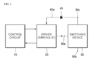
- a driving circuit of a semiconductor switching device for an electric power control is configured to include a driver circuit unit 20 and a control circuit 10.
- a reference numeral 30 is a semiconductor switching device (hereinafter, referred to as a switching device) which is a target of an ON or OFF driving of a driving circuit.
- the switching device 30 may be typically configured with the IGBT or the MOSFET described above.
- the switching device 30 may have an emitter, a gate, and a collector, and may be turned on or off according to a voltage difference between the emitter and the gate. For example, the switching device 30 is turned on when a voltage difference between the emitter and the gate is in a range of 12 to 20 volts (V), whereas it is turned off when the voltage difference between the emitter and the gate is in a range of 0 to 11 V.
- V volts
- a voltage difference between the emitter and the collector is decreased from ten to tens of volts in an OFF state to 2 to 3 volts, and it may be determined whether or not the switching device 30 is in an ON state by detecting a collector voltage. However, according to an amount of current flowing between the emitter and the collector, a variation of a voltage difference therebetween may occur.
- the driver circuit unit 20 is connected to the gate and the collector of the switching device 30, and is a circuit unit which outputs a driving signal to the gate to drive the switching device 30 to an ON state or stops the outputting of the driving signal to change the switching device 30 from the ON state to an OFF state.
- the driving signal may be a current signal of, for example, about several amperes, or a voltage signal of, for example, ten to tens of volts.
- the driver circuit unit 20 may be configured with an integrated circuit for outputting the driving signal.
- the driver circuit unit 20 may receive a voltage detection signal representing a collector voltage value of the switching device 30 from the collector thereof.
- a reference numeral 40a represents a transmission side circuit which transmits the voltage detection signal to the driver circuit unit 20.
- a reference numeral 40 represents a protective diode of the transmission side circuit 40a, which is conducting when a voltage of the transmission side circuit 40a is higher than a collector voltage of the switching device 30.
- the driver circuit unit 20 provides the control circuit 10 with the collector voltage value according to the voltage detection signal received from the collector of the switching device 30 and a monitoring signal representing a state of the driver circuit unit 20. Further, in FIG. 1 , an arrow indicating a left side between the driver circuit unit 20 and the control circuit 10 shows a transmission of the monitoring signal.
- the control circuit 10 is connected to the driver circuit unit 20 to output an ON or OFF control instruction signal regarding the switching device 30 to the driver circuit unit 20.
- an arrow indicating a right side between the driver circuit unit 20 and the control circuit 10 shows a transmission of the ON or OFF control instruction signal.
- control circuit 10 may determine a current ON/OFF state of the switching device 30 and a current state of the driver circuit unit 20 based on the monitoring signal provided from the driver circuit unit 20.
- the driving circuit of a semiconductor switching device for an electric power control is configured to perform an ON/OFF driving and a state monitoring of the switching device 30 by means of only the single driver circuit unit 20. Consequently, when a malfunction such as a burning of the single driver circuit unit 20 occurs, there is a problem in which the ON/OFF driving and the state monitoring of the switching device 30 are broken down.
- an object of the present disclosure is to provide a driving circuit of a switching device for an electric power control capable of improving reliability of an ON/OFF driving and a state monitoring operation of the switching device by configuring a multiplexing configuration for the ON/OFF driving and the state monitoring operation of the switching device.
- the object of the present disclosure may be obtained by providing a driving circuit of a switching device for an electric power control which includes a driver circuit unit connected to the switching device and configured to control the switching device to an ON state or an OFF state, a first logic device connected to the switching device and the driver circuit unit and configured to transmit an ON or OFF control signal regarding the switching device to the driver circuit unit or to provide a monitoring signal detecting an ON state or an OFF state of the switching device to the driver circuit unit, a second logic device connected to the switching device and the first logic device and configured to transmit an ON or OFF control signal regarding the switching device to the first logic device or to provide a monitoring signal detecting an ON state or an OFF state of the switching device to the first logic device, and a controller connected to the first logic device and the second logic device and configured to provide an ON or OFF control instruction signal regarding the switching device to at least one of the first logic device and the second logic device.
- the driver circuit unit may include a plurality of driver circuits commonly connected to the switching device in duplicate and configured to control the switching device to be turn on or off.
- the first logic device and the second logic device may be connected to a gate and a collector of the switching device so as to receive the monitoring signal detecting the ON state or the OFF state of the switching device.
- level down shifters connected between the second logic device and the gate of the switching device, between the second logic device and the collector of the switching device, and between the first logic device and the gate of the switching device, respectively, and configured to lower a voltage level of the monitoring signal may be further included.
- the controller when the monitoring signals regarding the ON state or the OFF state of the switching device are different from each other, which are received from the first logic device and the second logic device, respectively, the controller may be configured to determine that an abnormality occurs in one of the first logic device and the second logic device.
- the controller may be configured to determine a logic device in which an abnormality occurs out of the first logic device and the second logic device based on the ON or OFF control instruction signal and the monitoring signals regarding the ON state or the OFF state of the switching device, which are received from the first logic device and the second logic device, respectively.
- each of the first logic device and the second logic device may be configured with one of a field programmable gate array (FPGA), a microcomputer unit (MCU), a complex programmable logic device (CPLD), and an application-specific integrated circuit (ASIC).
- FPGA field programmable gate array
- MCU microcomputer unit
- CPLD complex programmable logic device
- ASIC application-specific integrated circuit
- a resistor connected between the driver circuit unit and the gate of the switching device and configured to make a gate driving signal for controlling the switching device to an ON state or an OFF state into a predetermined voltage signal may be further included.
- the level down shifters may be configured with one of a resistor rail, a comparator, and an operational amplifier.
- the driving circuit of a switching device of an electric power control may include a logic device connected between the driver circuit unit and the controller and configured to transmit an ON or OFF control instruction signal regarding the switching device to the driver circuit unit and to monitor an ON state or an OFF state of the switching device to transmit the monitoring result, and may be configured to have a multiplexing configuration of the logic devices, thereby providing effectiveness capable of improving reliability of an ON/OFF control and a monitoring operation of the switching device in comparison with the related art.
- the driver circuit unit may be configured with a plurality of driver circuits such that it may be possible to provide effectiveness capable of preventing a breakdown of an OF/OFF control and a monitoring operation of the switching device even when a malfunction occurs in one of the plurality of driver circuits.
- the first logic device and the second logic device may detect and calculate a gate voltage and a collector voltage of the switching device and a voltage difference therebetween such that it may be possible to provide effectiveness capable of exactly determining an ON state or an OFF state of the switching device.
- the driving circuit of a switching device for an electric power control may further include the level down shifters, so that it may be possible to provide effectiveness capable of lowering and providing a voltage level of a monitoring signal to a level suitable for an input voltage of the first logic device and the second logic device.
- the controller may determine that one of the first logic device and the second logic device is abnormal, by means of the logic circuits included in the controller or the process program, so that it may be possible to provide effectiveness capable of monitoring whether or not the logic devices are in a normal state.
- the driving circuit of a switching device for an electric power control may provide effectiveness that the controller may exactly determine a logic device in which an abnormality occurs out of the first logic device and the second logic device based on data of the ON or OFF control instruction signal output from the controller and the monitoring signals regarding an ON state or an OFF state of the switching device.
- each of the first logic device and the second logic device may be configured with one of an FPGA, an MCU, a CPLD, and an ASIC, so that it may be possible to provide effectiveness capable of selectively configuring the logic device.
- the driving circuit of a switching device of an electric power control may include the resistor connected between the driver circuit unit and the gate of the switching device, so that it may be possible to provide effectiveness capable of making the gate driving signal into a predetermined voltage signal.
- the level down shifters may be configured with one of a resistor rail, a comparator, and an operational amplifier, so that it may be possible to provide effectiveness capable of selectively configuring the level down shifters.
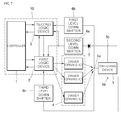
- a driving circuit of a switching device for an electric power control may be configured to include a driver circuit unit 4, a first logic device 2, a second logic device 3, and a controller 1.
- a reference numeral 5 represents a switching device for an electric power control (hereinafter, referred to as a switching device) configured with, for example, an IGBT or a MOSFET, and includes a gate 5a, an emitter 5b, and a collector 5c.
- a switching device configured with, for example, an IGBT or a MOSFET, and includes a gate 5a, an emitter 5b, and a collector 5c.
- the switching device 5 is turned on or off according to a voltage difference between the emitter 5b and the gate 5a.
- the switching device 5 is turned on when a voltage difference between the emitter 5b and the gate 5a is in a range of 12 to 20 V, whereas it is turned off when a voltage difference between the emitter 5b and the gate 5a is in a range of 0 to 11 V.
- a voltage difference between the emitter 5b and the collector 5c is decreased from ten to tens of volts in an OFF state to 2 to 3 volts, and it may be determined whether or not the switching device 5 is in an ON state by detecting a collector voltage.
- the emitter 5b of the switching device 5 may be connected to a ground of a circuit or a ground of a printed circuit board.
- an output terminal (See a right arrow of the connector in FIG. 2 ) of the collector 5c of the switching device 5 may be connected to an electric power supply unit for an electric power conversion or a circuit unit required for an electric power switching.
- the driver circuit unit 4 is connected to the switching device 5 and provides a driving signal thereto so as to control the switching device 5 to an ON state or an OFF state.
- the driving signal may be a current signal of, for example, several amperes, or a voltage signal of, for example, ten to tens of volts.
- the driver circuit unit 4 may be configured with an integrated circuit for outputting the driving signal.
- the driver circuit unit 4 is configured to include a plurality of driver circuits, and the plurality of driver circuits are commonly connected in duplicate to the single switching device 5 in parallel.
- a resistor which makes a gate driving signal for controlling the switching device 5 to an ON state or an OFF state into a predetermined voltage signal, may be connected between the driver circuit unit 4 and the gate 5a of the switching device 5.
- the first logic device 2 is connected to the switching device 5 and the driver circuit unit 4 to transmit an ON or OFF control signal regarding the switching device 5 to the driver circuit unit 4, or to provide the driver circuit unit 4 with a monitoring signal detecting an ON state or an OFF state of the switching device 5.
- the second logic device 3 is connected to the switching device 5 and the first logic device 2 to transmit an ON or OFF control signal regarding the switching device 5 to the first logic device 2, or to provide the first logic device 2 with a monitoring signal detecting an ON state or an OFF state of the switching device 5.
- the first logic device 2 and the second logic device 2 are connected to the gate 5a and the collector 5c of the switching device 5, respectively.
- Each of the first logic device 2 and the second logic device 3 may be configured with one of a field programmable gate array (FPGA), a microcomputer unit (MCU), a complex programmable logic device (CPLD), and an application-specific integrated circuit (ASIC).
- FPGA field programmable gate array
- MCU microcomputer unit
- CPLD complex programmable logic device
- ASIC application-specific integrated circuit
- the driving circuit of a switching device for an electric power control includes a first level down shifter 6b, a second level down shifter 6a, and a third level down shifter 6c.
- the first level down shifter 6b, the second level down shifter 6a, and the third level down shifter 6c are connected between the second logic device 3 and the gate 5a of the switching device 5, between the first and second logic devices 2 and 3 and the collector 5c of the switching device 5, and between the first logic device 2 and the gate 5a of the switching device 5, respectively, thereby lowering a voltage level of the monitoring signal.
- each of the first level down shifter 6b, the second level down shifter 6a, and the third level down shifter 6c may lower a voltage level of the monitoring signal to a voltage level of, for example, 3.3 volts suitable for an input voltage level of the first logic device 2 and the second logic device 3, thereby providing the lowered voltage thereto.
- each of the first level down shifter 6b, the second level down shifter 6a, and the third level down shifter 6c may be configured with one of a resistor rail, a comparator, and an operational amplifier.
- a diode 7 for protecting a circuit to a transmission path of a monitoring signal is connected between the second level down shifter 6a and the collector 5c of the switching device 5.
- the transmission path transmitting a collector voltage representing an ON state or an OFF state of the switching device 5 to the second logic device 3, that is, a voltage of an output terminal of the second level down shifter 6a is higher than that of the collector 5c of the switching device 5, the diode 7 is conducting. Otherwise, the diode 7 is not conducting to protect the second level down shifter 6a, the second logic device 3, and the controller 1, which are disposed in a post-stage.
- the controller 1 is connected to the first logic device 2 and the second logic device 3, and may provide an ON or OFF control instruction signal regarding the switching device 5 to at least one of the first logic device 2 and the second logic device 3.
- controller 1 may determine an abnormal state of at least one of the first logic device 2 and the second logic device 3 based on the monitoring signals therefrom.
- the controller 1 may be configured with a microcomputer including a central processing unit for performing an arithmetic operation and a process based on a process program, a process program, a reference value, and a memory for storing a value of the arithmetic operation.
- the controller 1 may be configured to determine that one of the first logic device 2 and the second logic device 3 is abnormal.
- the controller 1 may be configured with a logic circuit for such a logical determination, and may be configured to have a structure in which a central processing unit reads a process program from a memory and compares the monitoring signals with each other according to the process program to determine whether or not the monitoring signals are the same as each other.
- the controller 1 may be configured to exactly determine a logic device in which an abnormality (malfunction) occurs out of the first logic device 2 and the second logic device 3 based on the ON or OFF control instruction signal, and the monitoring signals regarding an ON state or an OFF state of the switching device 5 which are received from the first logic device 2 and the second logic device 3, respectively.
- the controller 1, the first logic device 2, and the second logic device 3 may be configured as a single control circuit 10.
- the controller 1 When the controller 1 outputs an ON or OFF control instruction signal so as to turn on or off the switching device 5, the first logic device 2 and the second logic device 3 receive the ON or OFF control instruction signal in Operation S1.
- the first logic device 2 transmits an ON or OFF control signal regarding the switching device 5 to the driver circuit unit 4.
- the plurality of driver circuits configuring the driver circuit unit 4 commonly provide the gate 5a of the switching device 5 with gate driving signals in duplicate in Operation S3.
- the plurality of driver circuits configuring the driver circuit unit 4 commonly do not output the gate driving signals to the gate 5a of the switching device 5 in Operation S5.
- a voltage difference between the emitter 5b and the collector 5c is decreased from ten to tens of volts in an OFF state to 2 to 3 volts.
- a collector voltage is also decreased to 2 to 3 volts to be lower than a voltage at the transmission path of the monitoring signal, that is, a voltage between the second level down shifter 6a and the diode 7. Consequently, the diode 7 is conducting and an ON state monitoring signal of the switching device 5 represented as a collector voltage is transmitted to the second logic device 3 and the first logic device 2 via the diode 7 and the second down shifter 6a in Operation S7.
- the collector voltage is increased to tens of volts to be greater than a voltage at the transmission path of the monitoring signal, that is, a voltage between the second level down shifter 6a and the diode 7.
- the diode 7 is not conducting and an OFF state monitoring signal of the switching device 5 represented as the collector voltage is not transmitted to the post-stage circuit of the diode 7 so that the second logic device 3 and the first logic device 2 do not receive the OFF state monitoring signal.
- an ON state monitoring signal of the switching device 5 represented by a gate voltage of about 12 to 20 volts thereof is also transmitted to the second logic device 3 through the first level down shifter 6b. And, the ON state monitoring signal is transmitted to the first logic device 2 through the third level down shifter 6c in Operation S8.
- an OFF state monitoring signal of the switching device 5 represented by a gate voltage close to about 0 volts thereof is also transmitted to the second logic device 3 through the first level down shifter 6b. And, the OFF state monitoring signal is transmitted to the first logic device 2 through the third level down shifter 6c.
- each of the second logic device 3 and the first logic device 2 compares the collector voltage and the gate voltage with reference voltage values (that is, a reference collector voltage value and a reference gate voltage value which are predetermined when a switching device is in an ON state) through internal logic circuits such as a comparator, an AND gate and the like which are not shown. Thereafter, an ON state or an OFF state of the switching device 5 is exactly determined by performing a logical operation (for example, an AND operation) on two comparison results through the internal logic circuits in Operation S9.
- a logical operation for example, an AND operation
- the monitoring signals regrading an ON state or an OFF state of the switching device 5, which are determined by the second logic device 3 and the first logic device 2, respectively, are transmitted to the controller 1.
- the controller 1 compares values with each other whether or not the values are the same as each other, which are represented by the monitoring signals regarding an ON state or an OFF state of the switching device 5 and determined by the second logic device 3 and the first logic device 2, respectively. Therefore, an abnormality occurrence of the second logic device 3 or the first logic device 2 may be determined in Operation S10.
- the controller 1 may determine that the second logic device 3 and the first logic device 2 are normal in Operation S 11.
- the controller 1 may determine that an abnormality (malfunction) occurs in one of the second logic device 3 and the first logic device 2 in Operation S12.
- the controller 1 may exactly determine a logic device in which an abnormality (malfunction) occurs out of the second logic device 3 and the first logic device 2 in Operations S13 and S14.
- the second logic device 3 provides a monitoring signal representing an ON state of the switching device 5 to the controller 1. And, if the first logic device 2 has provided the controller 1 with a monitoring signal representing an OFF state of the switching device 5, the controller 1 may determine an abnormality (malfunction) occurrence of the first logic device 2.
- the driving circuit of a switching device for an electric power control may provide effectiveness capable of improving reliability of an ON/OFF control and a monitoring operation of a switching device in comparison with the related art by configuring a logic device and/or a driver circuit in plural numbers.
- effectiveness may be provided to prevent an occurrence of a breakdown of the ON/OFF control and the monitoring operation of the switching device even when a malfunction occurs in any one of the driver circuits, since the driver circuit unit is configured with a plurality of driver circuits.
- the controller determines that one of the first logic device and the second logic device is abnormal. Therefore, effectiveness may be provided to monitor whether or not the logic devices are in a normal state.
Landscapes
- Engineering & Computer Science (AREA)
- Computer Hardware Design (AREA)
- Power Engineering (AREA)
- Physics & Mathematics (AREA)
- Mathematical Physics (AREA)
- Computing Systems (AREA)
- General Engineering & Computer Science (AREA)
- Power Conversion In General (AREA)
- Electronic Switches (AREA)
Abstract
Description
- Embodiments of the present disclosure relate to a driving circuit of a switching device for an electric power control, and more particularly, to a driving circuit of a switching device for an electric power control capable of improving reliability of an ON/OFF driving and a status monitoring.
- For controlling electric power being supplied to an alternating current motor, a semiconductor switching device for an electric power control, such as an insulated gate bipolar transistor (IGBT), a metal oxide semiconductor field effect transistor (MOSFET) and the like, is used for an electric power conversion or an electric power control in which an alternating current is converted into a direct current and the direct current is again converted into the alternating current through an inverter.
- The present disclosure relates to a driving circuit of such a semiconductor switching device for an electric power control.
- In a driving circuit of such a semiconductor switching device for an electric power control, the related art will be described below with reference to
FIG. 1 . - As shown in
FIG. 1 , a driving circuit of a semiconductor switching device for an electric power control according to the related art is configured to include adriver circuit unit 20 and acontrol circuit 10. - In
FIG. 1 , areference numeral 30 is a semiconductor switching device (hereinafter, referred to as a switching device) which is a target of an ON or OFF driving of a driving circuit. - The
switching device 30 may be typically configured with the IGBT or the MOSFET described above. - The
switching device 30 may have an emitter, a gate, and a collector, and may be turned on or off according to a voltage difference between the emitter and the gate. For example, theswitching device 30 is turned on when a voltage difference between the emitter and the gate is in a range of 12 to 20 volts (V), whereas it is turned off when the voltage difference between the emitter and the gate is in a range of 0 to 11 V. - Also, when the
switching device 30 is in an ON state, a voltage difference between the emitter and the collector is decreased from ten to tens of volts in an OFF state to 2 to 3 volts, and it may be determined whether or not theswitching device 30 is in an ON state by detecting a collector voltage. However, according to an amount of current flowing between the emitter and the collector, a variation of a voltage difference therebetween may occur. - The
driver circuit unit 20 is connected to the gate and the collector of theswitching device 30, and is a circuit unit which outputs a driving signal to the gate to drive theswitching device 30 to an ON state or stops the outputting of the driving signal to change theswitching device 30 from the ON state to an OFF state. Here, the driving signal may be a current signal of, for example, about several amperes, or a voltage signal of, for example, ten to tens of volts. - The
driver circuit unit 20 may be configured with an integrated circuit for outputting the driving signal. - The
driver circuit unit 20 may receive a voltage detection signal representing a collector voltage value of theswitching device 30 from the collector thereof. - A
reference numeral 40a represents a transmission side circuit which transmits the voltage detection signal to thedriver circuit unit 20. - In
FIG. 1 , areference numeral 40 represents a protective diode of thetransmission side circuit 40a, which is conducting when a voltage of thetransmission side circuit 40a is higher than a collector voltage of theswitching device 30. - Also, the
driver circuit unit 20 provides thecontrol circuit 10 with the collector voltage value according to the voltage detection signal received from the collector of theswitching device 30 and a monitoring signal representing a state of thedriver circuit unit 20. Further, inFIG. 1 , an arrow indicating a left side between thedriver circuit unit 20 and thecontrol circuit 10 shows a transmission of the monitoring signal. - The
control circuit 10 is connected to thedriver circuit unit 20 to output an ON or OFF control instruction signal regarding theswitching device 30 to thedriver circuit unit 20. InFIG. 1 , an arrow indicating a right side between thedriver circuit unit 20 and thecontrol circuit 10 shows a transmission of the ON or OFF control instruction signal. - Therefore, the
control circuit 10 may determine a current ON/OFF state of theswitching device 30 and a current state of thedriver circuit unit 20 based on the monitoring signal provided from thedriver circuit unit 20. - However, the driving circuit of a semiconductor switching device for an electric power control according to the related art is configured to perform an ON/OFF driving and a state monitoring of the
switching device 30 by means of only the singledriver circuit unit 20. Consequently, when a malfunction such as a burning of the singledriver circuit unit 20 occurs, there is a problem in which the ON/OFF driving and the state monitoring of theswitching device 30 are broken down. - Therefore, the present disclosure is provided to address the aforementioned problems, and an object of the present disclosure is to provide a driving circuit of a switching device for an electric power control capable of improving reliability of an ON/OFF driving and a state monitoring operation of the switching device by configuring a multiplexing configuration for the ON/OFF driving and the state monitoring operation of the switching device.
- The object of the present disclosure may be obtained by providing a driving circuit of a switching device for an electric power control which includes a driver circuit unit connected to the switching device and configured to control the switching device to an ON state or an OFF state, a first logic device connected to the switching device and the driver circuit unit and configured to transmit an ON or OFF control signal regarding the switching device to the driver circuit unit or to provide a monitoring signal detecting an ON state or an OFF state of the switching device to the driver circuit unit, a second logic device connected to the switching device and the first logic device and configured to transmit an ON or OFF control signal regarding the switching device to the first logic device or to provide a monitoring signal detecting an ON state or an OFF state of the switching device to the first logic device, and a controller connected to the first logic device and the second logic device and configured to provide an ON or OFF control instruction signal regarding the switching device to at least one of the first logic device and the second logic device.
- In accordance with one aspect of the present disclosure, the driver circuit unit may include a plurality of driver circuits commonly connected to the switching device in duplicate and configured to control the switching device to be turn on or off.
- In accordance with another aspect of the present disclosure, the first logic device and the second logic device may be connected to a gate and a collector of the switching device so as to receive the monitoring signal detecting the ON state or the OFF state of the switching device.
- In accordance with still another aspect of the present disclosure, level down shifters connected between the second logic device and the gate of the switching device, between the second logic device and the collector of the switching device, and between the first logic device and the gate of the switching device, respectively, and configured to lower a voltage level of the monitoring signal may be further included.
- In accordance with yet another aspect of the present disclosure, when the monitoring signals regarding the ON state or the OFF state of the switching device are different from each other, which are received from the first logic device and the second logic device, respectively, the controller may be configured to determine that an abnormality occurs in one of the first logic device and the second logic device.
- In accordance with yet another aspect of the present disclosure, the controller may be configured to determine a logic device in which an abnormality occurs out of the first logic device and the second logic device based on the ON or OFF control instruction signal and the monitoring signals regarding the ON state or the OFF state of the switching device, which are received from the first logic device and the second logic device, respectively.
- In accordance with yet another aspect of the present disclosure, each of the first logic device and the second logic device may be configured with one of a field programmable gate array (FPGA), a microcomputer unit (MCU), a complex programmable logic device (CPLD), and an application-specific integrated circuit (ASIC).
- In accordance with yet another aspect of the present disclosure, a resistor connected between the driver circuit unit and the gate of the switching device and configured to make a gate driving signal for controlling the switching device to an ON state or an OFF state into a predetermined voltage signal may be further included.
- In accordance with yet another aspect of the present disclosure, the level down shifters may be configured with one of a resistor rail, a comparator, and an operational amplifier.
- The driving circuit of a switching device of an electric power control according to the present disclosure may include a logic device connected between the driver circuit unit and the controller and configured to transmit an ON or OFF control instruction signal regarding the switching device to the driver circuit unit and to monitor an ON state or an OFF state of the switching device to transmit the monitoring result, and may be configured to have a multiplexing configuration of the logic devices, thereby providing effectiveness capable of improving reliability of an ON/OFF control and a monitoring operation of the switching device in comparison with the related art.
- In the driving circuit of a switching device for an electric power control according to the present disclosure, the driver circuit unit may be configured with a plurality of driver circuits such that it may be possible to provide effectiveness capable of preventing a breakdown of an OF/OFF control and a monitoring operation of the switching device even when a malfunction occurs in one of the plurality of driver circuits.
- In the driving circuit of a switching device for an electric power control according to the present disclosure, because of being connected to the gate and the collector of the switching device, the first logic device and the second logic device may detect and calculate a gate voltage and a collector voltage of the switching device and a voltage difference therebetween such that it may be possible to provide effectiveness capable of exactly determining an ON state or an OFF state of the switching device.
- The driving circuit of a switching device for an electric power control according to the present disclosure may further include the level down shifters, so that it may be possible to provide effectiveness capable of lowering and providing a voltage level of a monitoring signal to a level suitable for an input voltage of the first logic device and the second logic device.
- In the driving circuit of a switching device for an electric power control according to the present disclosure, when the monitoring signals regarding an ON state or an OFF state of the switching device are different from each other, which are received from the first logic device and the second logic device, respectively, the controller may determine that one of the first logic device and the second logic device is abnormal, by means of the logic circuits included in the controller or the process program, so that it may be possible to provide effectiveness capable of monitoring whether or not the logic devices are in a normal state.
- The driving circuit of a switching device for an electric power control according to the present disclosure may provide effectiveness that the controller may exactly determine a logic device in which an abnormality occurs out of the first logic device and the second logic device based on data of the ON or OFF control instruction signal output from the controller and the monitoring signals regarding an ON state or an OFF state of the switching device.
- In the driving circuit of a switching device for an electric power control according to the present disclosure, each of the first logic device and the second logic device may be configured with one of an FPGA, an MCU, a CPLD, and an ASIC, so that it may be possible to provide effectiveness capable of selectively configuring the logic device.
- The driving circuit of a switching device of an electric power control may include the resistor connected between the driver circuit unit and the gate of the switching device, so that it may be possible to provide effectiveness capable of making the gate driving signal into a predetermined voltage signal.
- In the driving circuit of a switching device for an electric power control, the level down shifters may be configured with one of a resistor rail, a comparator, and an operational amplifier, so that it may be possible to provide effectiveness capable of selectively configuring the level down shifters.
-
-
FIG. 1 is a block diagram illustrating a configuration of a driving circuit of a switching device for an electric power control according to the related art. -
FIG. 2 is a block diagram illustrating a configuration of a driving circuit of a switching device for an electric power control according to one preferred embodiment of the present disclosure. -
FIG. 3 is a flowchart illustrating an ON or OFF control instruction of a controller and an ON/OFF operation process of a switching device according to the ON or OFF control instruction in the driving circuit of a switching device for an electric power control according to one preferred embodiment of the present disclosure. -
FIG. 4 is a flowchart illustrating a process for a determination operation of an ON state or an OFF state of a switching device and an abnormality (malfunction) occurrence determination operation of a logic device in the driving circuit of a switching device for an electric power control. - Objects of the present disclosure described above, configurations for attaining these objects and effectiveness thereof will be apparently understood from the following description with reference to
FIG. 2 regarding a driving circuit of a switching device for an electric power control according to one preferred embodiment of the present disclosure. - With reference to
FIG. 2 , a driving circuit of a switching device for an electric power control according to one preferred embodiment of the present disclosure may be configured to include adriver circuit unit 4, afirst logic device 2, asecond logic device 3, and acontroller 1. - In
FIG. 2 , areference numeral 5 represents a switching device for an electric power control (hereinafter, referred to as a switching device) configured with, for example, an IGBT or a MOSFET, and includes agate 5a, anemitter 5b, and acollector 5c. - The
switching device 5 is turned on or off according to a voltage difference between theemitter 5b and thegate 5a. For example, theswitching device 5 is turned on when a voltage difference between theemitter 5b and thegate 5a is in a range of 12 to 20 V, whereas it is turned off when a voltage difference between theemitter 5b and thegate 5a is in a range of 0 to 11 V. - Also, when the
switching device 5 is in an ON state, a voltage difference between theemitter 5b and thecollector 5c is decreased from ten to tens of volts in an OFF state to 2 to 3 volts, and it may be determined whether or not theswitching device 5 is in an ON state by detecting a collector voltage. - According to a preferred embodiment, the
emitter 5b of theswitching device 5 may be connected to a ground of a circuit or a ground of a printed circuit board. - Also, according to a preferred embodiment, an output terminal (See a right arrow of the connector in
FIG. 2 ) of thecollector 5c of theswitching device 5 may be connected to an electric power supply unit for an electric power conversion or a circuit unit required for an electric power switching. - The
driver circuit unit 4 is connected to theswitching device 5 and provides a driving signal thereto so as to control theswitching device 5 to an ON state or an OFF state. - Here, the driving signal may be a current signal of, for example, several amperes, or a voltage signal of, for example, ten to tens of volts.
- The
driver circuit unit 4 may be configured with an integrated circuit for outputting the driving signal. - In accordance with one preferred aspect of the present disclosure, even when a malfunction occurs in any one driver circuit unit, a breakdown of an ON/OFF control and a monitoring operation of the
switching device 5 may be prevented. For this purpose, thedriver circuit unit 4 is configured to include a plurality of driver circuits, and the plurality of driver circuits are commonly connected in duplicate to thesingle switching device 5 in parallel. - In accordance with one preferred aspect of the present disclosure, a resistor, which makes a gate driving signal for controlling the
switching device 5 to an ON state or an OFF state into a predetermined voltage signal, may be connected between thedriver circuit unit 4 and thegate 5a of theswitching device 5. - The
first logic device 2 is connected to theswitching device 5 and thedriver circuit unit 4 to transmit an ON or OFF control signal regarding theswitching device 5 to thedriver circuit unit 4, or to provide thedriver circuit unit 4 with a monitoring signal detecting an ON state or an OFF state of theswitching device 5. - The
second logic device 3 is connected to theswitching device 5 and thefirst logic device 2 to transmit an ON or OFF control signal regarding theswitching device 5 to thefirst logic device 2, or to provide thefirst logic device 2 with a monitoring signal detecting an ON state or an OFF state of theswitching device 5. - In order to receive the monitoring signal detecting an ON state or an OFF state of the
switching device 5, thefirst logic device 2 and thesecond logic device 2 are connected to thegate 5a and thecollector 5c of theswitching device 5, respectively. - Each of the
first logic device 2 and thesecond logic device 3 may be configured with one of a field programmable gate array (FPGA), a microcomputer unit (MCU), a complex programmable logic device (CPLD), and an application-specific integrated circuit (ASIC). - The driving circuit of a switching device for an electric power control according to one preferred embodiment of the present disclosure includes a first level down
shifter 6b, a second level downshifter 6a, and a third level downshifter 6c. - The first level down
shifter 6b, the second level downshifter 6a, and the third level downshifter 6c are connected between thesecond logic device 3 and thegate 5a of theswitching device 5, between the first andsecond logic devices collector 5c of theswitching device 5, and between thefirst logic device 2 and thegate 5a of theswitching device 5, respectively, thereby lowering a voltage level of the monitoring signal. In other words, each of the first level downshifter 6b, the second level downshifter 6a, and the third level downshifter 6c may lower a voltage level of the monitoring signal to a voltage level of, for example, 3.3 volts suitable for an input voltage level of thefirst logic device 2 and thesecond logic device 3, thereby providing the lowered voltage thereto. - In accordance with one preferred aspect of the present disclosure, each of the first level down
shifter 6b, the second level downshifter 6a, and the third level downshifter 6c may be configured with one of a resistor rail, a comparator, and an operational amplifier. - With reference to
FIG. 2 , adiode 7 for protecting a circuit to a transmission path of a monitoring signal is connected between the second level downshifter 6a and thecollector 5c of theswitching device 5. - When a voltage at a transmission path of a monitoring signal, the transmission path transmitting a collector voltage representing an ON state or an OFF state of the
switching device 5 to thesecond logic device 3, that is, a voltage of an output terminal of the second level downshifter 6a is higher than that of thecollector 5c of theswitching device 5, thediode 7 is conducting. Otherwise, thediode 7 is not conducting to protect the second level downshifter 6a, thesecond logic device 3, and thecontroller 1, which are disposed in a post-stage. - The
controller 1 is connected to thefirst logic device 2 and thesecond logic device 3, and may provide an ON or OFF control instruction signal regarding theswitching device 5 to at least one of thefirst logic device 2 and thesecond logic device 3. - Also, the
controller 1 may determine an abnormal state of at least one of thefirst logic device 2 and thesecond logic device 3 based on the monitoring signals therefrom. - According to one embodiment, the
controller 1 may be configured with a microcomputer including a central processing unit for performing an arithmetic operation and a process based on a process program, a process program, a reference value, and a memory for storing a value of the arithmetic operation. - When the monitoring signals regarding an ON state or an OFF state of the
switching device 5 are different from each other, which are received from thefirst logic device 2 and thesecond logic device 3, respectively, thecontroller 1 may be configured to determine that one of thefirst logic device 2 and thesecond logic device 3 is abnormal. For this purpose, thecontroller 1 may be configured with a logic circuit for such a logical determination, and may be configured to have a structure in which a central processing unit reads a process program from a memory and compares the monitoring signals with each other according to the process program to determine whether or not the monitoring signals are the same as each other. - The
controller 1 may be configured to exactly determine a logic device in which an abnormality (malfunction) occurs out of thefirst logic device 2 and thesecond logic device 3 based on the ON or OFF control instruction signal, and the monitoring signals regarding an ON state or an OFF state of theswitching device 5 which are received from thefirst logic device 2 and thesecond logic device 3, respectively. - The
controller 1, thefirst logic device 2, and thesecond logic device 3 may be configured as asingle control circuit 10. - An operation of the driving circuit configured as described above of a switching device for an electric power control according to the present disclosure will be described with reference to
FIGS. 2 and3 . - Firstly, an ON or OFF control instruction of the
controller 1 and an ON/OFF operation of a switching device according thereto will be described. - When the
controller 1 outputs an ON or OFF control instruction signal so as to turn on or off theswitching device 5, thefirst logic device 2 and thesecond logic device 3 receive the ON or OFF control instruction signal in Operation S1. - And, in response to the ON or OFF control instruction signal, the
first logic device 2 transmits an ON or OFF control signal regarding theswitching device 5 to thedriver circuit unit 4. - When the signal transmitted from the
first logic device 2 is an ON control instruction signal ("YES" in Operation S2), the plurality of driver circuits configuring thedriver circuit unit 4 commonly provide thegate 5a of theswitching device 5 with gate driving signals in duplicate in Operation S3. - On the other hand, when the signal transmitted from the
first logic device 2 is an OFF control instruction signal ("NO" in Operation S2), the plurality of driver circuits configuring thedriver circuit unit 4 commonly do not output the gate driving signals to thegate 5a of theswitching device 5 in Operation S5. - When the
driver circuit unit 4 outputs the gate driving signals, a voltage difference between an emitter voltage which is a ground potential of theswitching device 5 and a gate voltage formed by the gate driving signals is greatly increased to about 12 to 20 volts. Consequently, theswitching device 5 is to be an ON state (that is, is turned on) in Operation S4. - On the other hand, when the
driver circuit unit 4 does not output the gate driving signals, a voltage difference between the emitter voltage which is the ground potential of theswitching device 5 and a gate voltage formed by the gate driving signals is greatly decreased to about 0 to 11 volts. Consequently, theswitching device 5 is to be an OFF state (that is, is turned off) in Operation S6. - Next, a determination operation regarding an ON state or an OFF state of the
switching device 5 and an abnormality (malfunction) occurrence determination operation of a logic device will be described with reference toFIGS. 2 and4 . - When the
switching device 5 is in an ON state, a voltage difference between theemitter 5b and thecollector 5c is decreased from ten to tens of volts in an OFF state to 2 to 3 volts. - As a result, a collector voltage is also decreased to 2 to 3 volts to be lower than a voltage at the transmission path of the monitoring signal, that is, a voltage between the second level down
shifter 6a and thediode 7. Consequently, thediode 7 is conducting and an ON state monitoring signal of theswitching device 5 represented as a collector voltage is transmitted to thesecond logic device 3 and thefirst logic device 2 via thediode 7 and thesecond down shifter 6a in Operation S7. - Also, in Operation S8, when the
switching device 5 is in an OFF state, a voltage difference between theemitter 5b and thecollector 5c is increased to ten to tens of volts. - Therefore, the collector voltage is increased to tens of volts to be greater than a voltage at the transmission path of the monitoring signal, that is, a voltage between the second level down
shifter 6a and thediode 7. As a result, thediode 7 is not conducting and an OFF state monitoring signal of theswitching device 5 represented as the collector voltage is not transmitted to the post-stage circuit of thediode 7 so that thesecond logic device 3 and thefirst logic device 2 do not receive the OFF state monitoring signal. - In addition, an ON state monitoring signal of the
switching device 5 represented by a gate voltage of about 12 to 20 volts thereof is also transmitted to thesecond logic device 3 through the first level downshifter 6b. And, the ON state monitoring signal is transmitted to thefirst logic device 2 through the third level downshifter 6c in Operation S8. - Further, in Operation S8, when the
switching device 5 is in an OFF state, an OFF state monitoring signal of theswitching device 5 represented by a gate voltage close to about 0 volts thereof is also transmitted to thesecond logic device 3 through the first level downshifter 6b. And, the OFF state monitoring signal is transmitted to thefirst logic device 2 through the third level downshifter 6c. - Then, each of the
second logic device 3 and thefirst logic device 2 compares the collector voltage and the gate voltage with reference voltage values (that is, a reference collector voltage value and a reference gate voltage value which are predetermined when a switching device is in an ON state) through internal logic circuits such as a comparator, an AND gate and the like which are not shown. Thereafter, an ON state or an OFF state of theswitching device 5 is exactly determined by performing a logical operation (for example, an AND operation) on two comparison results through the internal logic circuits in Operation S9. - The monitoring signals regrading an ON state or an OFF state of the
switching device 5, which are determined by thesecond logic device 3 and thefirst logic device 2, respectively, are transmitted to thecontroller 1. - Then, the
controller 1 compares values with each other whether or not the values are the same as each other, which are represented by the monitoring signals regarding an ON state or an OFF state of theswitching device 5 and determined by thesecond logic device 3 and thefirst logic device 2, respectively. Therefore, an abnormality occurrence of thesecond logic device 3 or thefirst logic device 2 may be determined in Operation S10. - Here, when the values are the same as each other, which are represented by the monitoring signals regarding an ON state or an OFF state of the
switching device 5 and determined by thesecond logic device 3 and thefirst logic device 2, respectively, thecontroller 1 may determine that thesecond logic device 3 and thefirst logic device 2 are normal inOperation S 11. - On the other hand, when the values are different from each other, which are represented by the monitoring signals regarding an ON state or an OFF state of the
switching device 5 and determined by thesecond logic device 3 and thefirst logic device 2, respectively, thecontroller 1 may determine that an abnormality (malfunction) occurs in one of thesecond logic device 3 and thefirst logic device 2 in Operation S12. - Also, by considering the ON or OFF control instruction signal output originally from the
controller 1 as well as whether or not the values are the same as each other, which are represented by the monitoring signals regarding an ON state or an OFF state of theswitching device 5 and determined by thesecond logic device 3 and thefirst logic device 2, respectively, thecontroller 1 may exactly determine a logic device in which an abnormality (malfunction) occurs out of thesecond logic device 3 and thefirst logic device 2 in Operations S13 and S14. - That is, in a state that the
controller 1 has output an ON control instruction signal for example, thesecond logic device 3 provides a monitoring signal representing an ON state of theswitching device 5 to thecontroller 1. And, if thefirst logic device 2 has provided thecontroller 1 with a monitoring signal representing an OFF state of theswitching device 5, thecontroller 1 may determine an abnormality (malfunction) occurrence of thefirst logic device 2. - As described above, the driving circuit of a switching device for an electric power control according to the present disclosure may provide effectiveness capable of improving reliability of an ON/OFF control and a monitoring operation of a switching device in comparison with the related art by configuring a logic device and/or a driver circuit in plural numbers.
- Also, effectiveness may be provided to prevent an occurrence of a breakdown of the ON/OFF control and the monitoring operation of the switching device even when a malfunction occurs in any one of the driver circuits, since the driver circuit unit is configured with a plurality of driver circuits.
- In addition, by means of the logic circuits included in the controller or the process program, when the monitoring signals regarding an ON state or an OFF state of the switching device are different from each other, which are received from the first logic device and the second logic device, respectively, the controller determines that one of the first logic device and the second logic device is abnormal. Therefore, effectiveness may be provided to monitor whether or not the logic devices are in a normal state.
Claims (8)
- A driving circuit of a switching device (5) for an electric power control, comprising:a driver circuit unit (4) connected to the switching device (5) and configured to control the switching device (5) to an ON state or an OFF state;a first logic device (2) connected to the switching device (5) and the driver circuit unit (4) and configured to transmit an ON or OFF control signal regarding the switching device (5) to the driver circuit unit (4) or to provide a monitoring signal detecting an ON state or an OFF state of the switching device (5) to the driver circuit unit (4);a second logic device (3) connected to the switching device (5) and the first logic device (2) and configured to transmit an ON or OFF control signal regarding the switching device (5) to the first logic device (2) or to provide a monitoring signal detecting an ON state or an OFF state of the switching device (5) to the first logic device (2); anda controller (1) connected to the first logic device (2) and the second logic device (3) and configured to provide an ON or OFF control instruction signal regarding the switching device (5) to at least one of the first logic device (2) and the second logic device (3).
- The driving circuit of claim 1, wherein the driver circuit unit (4) includes a plurality of driver circuits commonly connected to the switching device (5) in duplicate and configured to control the switching device (5) to be turn on or off.
- The driving circuit of claim 1, wherein the first logic device (2) and the second logic device (3) are connected to a gate (5a) and a collector (5c) of the switching device (5) so as to receive the monitoring signal detecting the ON state or the OFF state of the switching device (5).
- The driving circuit of claim 3, wherein further comprising:level down shifters (6a, 6b, 6c) connected between the second logic device (3) and the gate (5a) of the switching device (5), between the second logic device (3) and the collector (5c) of the switching device (5), and between the first logic device (2) and the gate (5a) of the switching device (5), respectively, and configured to lower a voltage level of the monitoring signal.
- The driving circuit of claim 1, wherein when the monitoring signals regarding the ON state and the OFF state of the switching device (5) are different from each other, which are received from the first logic device (2) and the second logic device (3), respectively, the controller (1) determines that an abnormality occurs in one of the first logic device (2) and the second logic device (3).
- The driving circuit of claim 1, wherein the controller (1) determines a logic device in which an abnormality occurs out of the first logic device (2) and the second logic device (3) based on the ON or OFF control instruction signal and the monitoring signals regarding the ON state or the OFF state of the switching device (5), which are received from the first logic device (2) and the second logic device (3), respectively.
- The driving circuit of claim 1, wherein each of the first logic device (2) and the second logic device (3) is configured with one of a field programmable gate array (FPGA), a microcomputer unit (MCU), a complex programmable logic device (CPLD), and an application-specific integrated circuit (ASIC).
- The driving circuit of claim 4, wherein the level down shifters (6a, 6b, 6c) are configured with one of a resistor rail, a comparator, and an operational amplifier.
Applications Claiming Priority (1)
| Application Number | Priority Date | Filing Date | Title |
|---|---|---|---|
| KR1020150101241A KR102021864B1 (en) | 2015-07-16 | 2015-07-16 | Driving circuit of switching device for electric power control |
Publications (2)
| Publication Number | Publication Date |
|---|---|
| EP3118996A1 true EP3118996A1 (en) | 2017-01-18 |
| EP3118996B1 EP3118996B1 (en) | 2020-06-17 |
Family
ID=56096512
Family Applications (1)
| Application Number | Title | Priority Date | Filing Date |
|---|---|---|---|
| EP16171921.6A Not-in-force EP3118996B1 (en) | 2015-07-16 | 2016-05-30 | Driving circuit of switching device for electric power control |
Country Status (6)
| Country | Link |
|---|---|
| US (1) | US9722600B2 (en) |
| EP (1) | EP3118996B1 (en) |
| JP (1) | JP6329998B2 (en) |
| KR (1) | KR102021864B1 (en) |
| CN (1) | CN106357258B (en) |
| ES (1) | ES2814099T3 (en) |
Families Citing this family (7)
| Publication number | Priority date | Publication date | Assignee | Title |
|---|---|---|---|---|
| KR101971701B1 (en) * | 2017-03-29 | 2019-08-16 | (주)스마트시스텍 | Switching driving device using fpga |
| US11049386B2 (en) | 2018-06-14 | 2021-06-29 | Eaton Intelligent Power Limited | Switch with current and voltage collection |
| US10783772B2 (en) * | 2018-06-14 | 2020-09-22 | Eaton Intelligent Power Limited | Wireless switch with three-way control |
| CN109980680B (en) * | 2018-12-24 | 2020-11-03 | 深圳供电局有限公司 | Microgrid system with safety protection function |
| US10873326B1 (en) | 2019-10-07 | 2020-12-22 | Eaton Intelligent Power Limited | Input voltage sensing using zero crossing detection |
| US10924116B1 (en) * | 2019-10-09 | 2021-02-16 | Semiconductor Components Industries, Llc | Analog switch multiplexer systems and related methods |
| CN111130525B (en) * | 2019-12-31 | 2024-03-15 | 北京旋极信息技术股份有限公司 | Control circuit, ignition device and switch control system |
Citations (5)
| Publication number | Priority date | Publication date | Assignee | Title |
|---|---|---|---|---|
| DE4100790A1 (en) * | 1991-01-12 | 1992-07-16 | Vdo Schindling | Monitoring power transistor made conductive by rectangular signal - setting memory element into state indicating defect according to voltage level during time window |
| EP1988633A1 (en) * | 2007-05-03 | 2008-11-05 | Honeywell International Inc. | Integrated gate driver for controlling and protecting power modules |
| US20090296433A1 (en) * | 2008-05-29 | 2009-12-03 | General Electric Company | Circuit and topology for very high reliability power electronics system |
| US20130234777A1 (en) * | 2010-10-29 | 2013-09-12 | Fujitsu Limited | Switching device of semiconductor circuit and switching method of the same |
| EP2814173A1 (en) * | 2013-06-13 | 2014-12-17 | General Electric Company | Insulated gate bipolar transistor failure mode detection and protection system and method |
Family Cites Families (10)
| Publication number | Priority date | Publication date | Assignee | Title |
|---|---|---|---|---|
| JPH04112225A (en) * | 1990-08-31 | 1992-04-14 | Nec Ic Microcomput Syst Ltd | Integrated circuit device |
| JP3564893B2 (en) * | 1996-09-02 | 2004-09-15 | 株式会社明電舎 | Gate drive circuit for voltage controlled switching element |
| KR100275037B1 (en) | 1997-12-30 | 2000-12-15 | 김형벽 | Massive power switching element (IGBT) drive control circuit. |
| KR100528674B1 (en) | 2000-08-18 | 2005-11-15 | 현대중공업 주식회사 | IGBT drive control circuit |
| FR2851056B1 (en) * | 2003-02-10 | 2005-04-08 | Alstom | METHOD AND SYSTEM FOR CONTROLLING ELECTRONIC POWER COMPONENT, AND INFORMATION RECORDING MEDIUM HAVING INSTRUCTIONS FOR PERFORMING THE METHOD |
| TW200849785A (en) * | 2007-06-15 | 2008-12-16 | Ind Tech Res Inst | DC-DC converter |
| US20110182094A1 (en) | 2007-08-13 | 2011-07-28 | The Powerwise Group, Inc. | System and method to manage power usage |
| JP5036466B2 (en) * | 2007-09-20 | 2012-09-26 | 東芝三菱電機産業システム株式会社 | Redundant control power conversion system and its soundness confirmation method |
| JP5991526B2 (en) * | 2012-09-18 | 2016-09-14 | 株式会社デンソー | Switching element drive IC |
| KR101836247B1 (en) | 2012-12-12 | 2018-03-08 | 현대자동차 주식회사 | Inverter driving apparatus |
-
2015
- 2015-07-16 KR KR1020150101241A patent/KR102021864B1/en active Active
-
2016
- 2016-05-30 EP EP16171921.6A patent/EP3118996B1/en not_active Not-in-force
- 2016-05-30 ES ES16171921T patent/ES2814099T3/en active Active
- 2016-07-13 CN CN201610551695.1A patent/CN106357258B/en active Active
- 2016-07-13 US US15/209,636 patent/US9722600B2/en active Active
- 2016-07-15 JP JP2016140150A patent/JP6329998B2/en not_active Expired - Fee Related
Patent Citations (5)
| Publication number | Priority date | Publication date | Assignee | Title |
|---|---|---|---|---|
| DE4100790A1 (en) * | 1991-01-12 | 1992-07-16 | Vdo Schindling | Monitoring power transistor made conductive by rectangular signal - setting memory element into state indicating defect according to voltage level during time window |
| EP1988633A1 (en) * | 2007-05-03 | 2008-11-05 | Honeywell International Inc. | Integrated gate driver for controlling and protecting power modules |
| US20090296433A1 (en) * | 2008-05-29 | 2009-12-03 | General Electric Company | Circuit and topology for very high reliability power electronics system |
| US20130234777A1 (en) * | 2010-10-29 | 2013-09-12 | Fujitsu Limited | Switching device of semiconductor circuit and switching method of the same |
| EP2814173A1 (en) * | 2013-06-13 | 2014-12-17 | General Electric Company | Insulated gate bipolar transistor failure mode detection and protection system and method |
Also Published As
| Publication number | Publication date |
|---|---|
| CN106357258A (en) | 2017-01-25 |
| US9722600B2 (en) | 2017-08-01 |
| EP3118996B1 (en) | 2020-06-17 |
| JP6329998B2 (en) | 2018-05-23 |
| US20170019098A1 (en) | 2017-01-19 |
| KR20170009362A (en) | 2017-01-25 |
| KR102021864B1 (en) | 2019-09-17 |
| CN106357258B (en) | 2019-03-29 |
| ES2814099T3 (en) | 2021-03-26 |
| JP2017028990A (en) | 2017-02-02 |
Similar Documents
| Publication | Publication Date | Title |
|---|---|---|
| EP3118996B1 (en) | Driving circuit of switching device for electric power control | |
| US8699193B2 (en) | Protection circuit for a power conversion apparatus | |
| KR102155973B1 (en) | Half-bridge driver fault diagnosis system and method | |
| US10804891B2 (en) | Driving device | |
| US10374593B2 (en) | Semiconductor device | |
| TWI436073B (en) | Test device for switchgear | |
| EP3059598B1 (en) | Electrical load controller with fault detection | |
| JP2015121418A (en) | Anomaly detection device for electric load driving device | |
| US8922258B2 (en) | Switching element driver IC and switching element driver device equipped with the same | |
| JPWO2018016225A1 (en) | In-vehicle control device | |
| US9515586B2 (en) | Power output stage, method for operation | |
| US10097172B2 (en) | Method for protecting a controllable semiconductor switch from overload and short-circuiting in a load circuit | |
| US20160025790A1 (en) | Short detection bus | |
| EP4116720A1 (en) | Power supply control apparatus and semiconductor failure detection method | |
| EP3382895A1 (en) | Electronic device provided with secondary failure preventing circuit | |
| CN110914643B (en) | Control device with a circuit for short-circuit protection of a ground line and a sensor, and method for short-circuit protection of a ground line and a sensor | |
| JP2016140119A (en) | Power supply | |
| JP2019198171A (en) | Power supply device | |
| US10978987B2 (en) | Motor drive device | |
| CN104081665A (en) | Circuit arrangement arranged on a carrier with temperature monitoring and method for detecting overheating | |
| CN108347158B (en) | Circuit protection system and method | |
| JP6469910B1 (en) | Overvoltage protection circuit | |
| JP6681357B2 (en) | Semiconductor device | |
| KR101470256B1 (en) | System and circuit for detecting a short between a sensor ground and a sensor supply output pin | |
| JP2007189844A (en) | Semiconductor element protection circuit |
Legal Events
| Date | Code | Title | Description |
|---|---|---|---|
| PUAI | Public reference made under article 153(3) epc to a published international application that has entered the european phase |
Free format text: ORIGINAL CODE: 0009012 |
|
| STAA | Information on the status of an ep patent application or granted ep patent |
Free format text: STATUS: THE APPLICATION HAS BEEN PUBLISHED |
|
| AK | Designated contracting states |
Kind code of ref document: A1 Designated state(s): AL AT BE BG CH CY CZ DE DK EE ES FI FR GB GR HR HU IE IS IT LI LT LU LV MC MK MT NL NO PL PT RO RS SE SI SK SM TR |
|
| AX | Request for extension of the european patent |
Extension state: BA ME |
|
| STAA | Information on the status of an ep patent application or granted ep patent |
Free format text: STATUS: REQUEST FOR EXAMINATION WAS MADE |
|
| 17P | Request for examination filed |
Effective date: 20170711 |
|
| RBV | Designated contracting states (corrected) |
Designated state(s): AL AT BE BG CH CY CZ DE DK EE ES FI FR GB GR HR HU IE IS IT LI LT LU LV MC MK MT NL NO PL PT RO RS SE SI SK SM TR |
|
| GRAP | Despatch of communication of intention to grant a patent |
Free format text: ORIGINAL CODE: EPIDOSNIGR1 |
|
| STAA | Information on the status of an ep patent application or granted ep patent |
Free format text: STATUS: GRANT OF PATENT IS INTENDED |
|
| INTG | Intention to grant announced |
Effective date: 20200110 |
|
| GRAS | Grant fee paid |
Free format text: ORIGINAL CODE: EPIDOSNIGR3 |
|
| GRAA | (expected) grant |
Free format text: ORIGINAL CODE: 0009210 |
|
| STAA | Information on the status of an ep patent application or granted ep patent |
Free format text: STATUS: THE PATENT HAS BEEN GRANTED |
|
| AK | Designated contracting states |
Kind code of ref document: B1 Designated state(s): AL AT BE BG CH CY CZ DE DK EE ES FI FR GB GR HR HU IE IS IT LI LT LU LV MC MK MT NL NO PL PT RO RS SE SI SK SM TR |
|
| REG | Reference to a national code |
Ref country code: GB Ref legal event code: FG4D |
|
| REG | Reference to a national code |
Ref country code: CH Ref legal event code: EP |
|
| REG | Reference to a national code |
Ref country code: DE Ref legal event code: R096 Ref document number: 602016038092 Country of ref document: DE |
|
| REG | Reference to a national code |
Ref country code: IE Ref legal event code: FG4D |
|
| REG | Reference to a national code |
Ref country code: AT Ref legal event code: REF Ref document number: 1282592 Country of ref document: AT Kind code of ref document: T Effective date: 20200715 |
|
| PG25 | Lapsed in a contracting state [announced via postgrant information from national office to epo] |
Ref country code: SE Free format text: LAPSE BECAUSE OF FAILURE TO SUBMIT A TRANSLATION OF THE DESCRIPTION OR TO PAY THE FEE WITHIN THE PRESCRIBED TIME-LIMIT Effective date: 20200617 Ref country code: GR Free format text: LAPSE BECAUSE OF FAILURE TO SUBMIT A TRANSLATION OF THE DESCRIPTION OR TO PAY THE FEE WITHIN THE PRESCRIBED TIME-LIMIT Effective date: 20200918 Ref country code: FI Free format text: LAPSE BECAUSE OF FAILURE TO SUBMIT A TRANSLATION OF THE DESCRIPTION OR TO PAY THE FEE WITHIN THE PRESCRIBED TIME-LIMIT Effective date: 20200617 Ref country code: NO Free format text: LAPSE BECAUSE OF FAILURE TO SUBMIT A TRANSLATION OF THE DESCRIPTION OR TO PAY THE FEE WITHIN THE PRESCRIBED TIME-LIMIT Effective date: 20200917 Ref country code: LT Free format text: LAPSE BECAUSE OF FAILURE TO SUBMIT A TRANSLATION OF THE DESCRIPTION OR TO PAY THE FEE WITHIN THE PRESCRIBED TIME-LIMIT Effective date: 20200617 |
|
| REG | Reference to a national code |
Ref country code: LT Ref legal event code: MG4D |
|
| REG | Reference to a national code |
Ref country code: NL Ref legal event code: MP Effective date: 20200617 |
|
| PG25 | Lapsed in a contracting state [announced via postgrant information from national office to epo] |
Ref country code: HR Free format text: LAPSE BECAUSE OF FAILURE TO SUBMIT A TRANSLATION OF THE DESCRIPTION OR TO PAY THE FEE WITHIN THE PRESCRIBED TIME-LIMIT Effective date: 20200617 Ref country code: LV Free format text: LAPSE BECAUSE OF FAILURE TO SUBMIT A TRANSLATION OF THE DESCRIPTION OR TO PAY THE FEE WITHIN THE PRESCRIBED TIME-LIMIT Effective date: 20200617 Ref country code: BG Free format text: LAPSE BECAUSE OF FAILURE TO SUBMIT A TRANSLATION OF THE DESCRIPTION OR TO PAY THE FEE WITHIN THE PRESCRIBED TIME-LIMIT Effective date: 20200917 Ref country code: RS Free format text: LAPSE BECAUSE OF FAILURE TO SUBMIT A TRANSLATION OF THE DESCRIPTION OR TO PAY THE FEE WITHIN THE PRESCRIBED TIME-LIMIT Effective date: 20200617 |
|
| REG | Reference to a national code |
Ref country code: AT Ref legal event code: MK05 Ref document number: 1282592 Country of ref document: AT Kind code of ref document: T Effective date: 20200617 |
|
| PG25 | Lapsed in a contracting state [announced via postgrant information from national office to epo] |
Ref country code: NL Free format text: LAPSE BECAUSE OF FAILURE TO SUBMIT A TRANSLATION OF THE DESCRIPTION OR TO PAY THE FEE WITHIN THE PRESCRIBED TIME-LIMIT Effective date: 20200617 Ref country code: AL Free format text: LAPSE BECAUSE OF FAILURE TO SUBMIT A TRANSLATION OF THE DESCRIPTION OR TO PAY THE FEE WITHIN THE PRESCRIBED TIME-LIMIT Effective date: 20200617 |
|
| PG25 | Lapsed in a contracting state [announced via postgrant information from national office to epo] |
Ref country code: SM Free format text: LAPSE BECAUSE OF FAILURE TO SUBMIT A TRANSLATION OF THE DESCRIPTION OR TO PAY THE FEE WITHIN THE PRESCRIBED TIME-LIMIT Effective date: 20200617 Ref country code: PT Free format text: LAPSE BECAUSE OF FAILURE TO SUBMIT A TRANSLATION OF THE DESCRIPTION OR TO PAY THE FEE WITHIN THE PRESCRIBED TIME-LIMIT Effective date: 20201019 Ref country code: CZ Free format text: LAPSE BECAUSE OF FAILURE TO SUBMIT A TRANSLATION OF THE DESCRIPTION OR TO PAY THE FEE WITHIN THE PRESCRIBED TIME-LIMIT Effective date: 20200617 Ref country code: EE Free format text: LAPSE BECAUSE OF FAILURE TO SUBMIT A TRANSLATION OF THE DESCRIPTION OR TO PAY THE FEE WITHIN THE PRESCRIBED TIME-LIMIT Effective date: 20200617 Ref country code: AT Free format text: LAPSE BECAUSE OF FAILURE TO SUBMIT A TRANSLATION OF THE DESCRIPTION OR TO PAY THE FEE WITHIN THE PRESCRIBED TIME-LIMIT Effective date: 20200617 Ref country code: RO Free format text: LAPSE BECAUSE OF FAILURE TO SUBMIT A TRANSLATION OF THE DESCRIPTION OR TO PAY THE FEE WITHIN THE PRESCRIBED TIME-LIMIT Effective date: 20200617 |
|
| PG25 | Lapsed in a contracting state [announced via postgrant information from national office to epo] |
Ref country code: PL Free format text: LAPSE BECAUSE OF FAILURE TO SUBMIT A TRANSLATION OF THE DESCRIPTION OR TO PAY THE FEE WITHIN THE PRESCRIBED TIME-LIMIT Effective date: 20200617 Ref country code: SK Free format text: LAPSE BECAUSE OF FAILURE TO SUBMIT A TRANSLATION OF THE DESCRIPTION OR TO PAY THE FEE WITHIN THE PRESCRIBED TIME-LIMIT Effective date: 20200617 Ref country code: IS Free format text: LAPSE BECAUSE OF FAILURE TO SUBMIT A TRANSLATION OF THE DESCRIPTION OR TO PAY THE FEE WITHIN THE PRESCRIBED TIME-LIMIT Effective date: 20201017 |
|
| REG | Reference to a national code |
Ref country code: DE Ref legal event code: R097 Ref document number: 602016038092 Country of ref document: DE |
|
| REG | Reference to a national code |
Ref country code: ES Ref legal event code: FG2A Ref document number: 2814099 Country of ref document: ES Kind code of ref document: T3 Effective date: 20210326 |
|
| PLBE | No opposition filed within time limit |
Free format text: ORIGINAL CODE: 0009261 |
|
| STAA | Information on the status of an ep patent application or granted ep patent |
Free format text: STATUS: NO OPPOSITION FILED WITHIN TIME LIMIT |
|
| PG25 | Lapsed in a contracting state [announced via postgrant information from national office to epo] |
Ref country code: DK Free format text: LAPSE BECAUSE OF FAILURE TO SUBMIT A TRANSLATION OF THE DESCRIPTION OR TO PAY THE FEE WITHIN THE PRESCRIBED TIME-LIMIT Effective date: 20200617 |
|
| 26N | No opposition filed |
Effective date: 20210318 |
|
| PG25 | Lapsed in a contracting state [announced via postgrant information from national office to epo] |
Ref country code: SI Free format text: LAPSE BECAUSE OF FAILURE TO SUBMIT A TRANSLATION OF THE DESCRIPTION OR TO PAY THE FEE WITHIN THE PRESCRIBED TIME-LIMIT Effective date: 20200617 |
|
| REG | Reference to a national code |
Ref country code: DE Ref legal event code: R119 Ref document number: 602016038092 Country of ref document: DE |
|
| REG | Reference to a national code |
Ref country code: CH Ref legal event code: PL |
|
| GBPC | Gb: european patent ceased through non-payment of renewal fee |
Effective date: 20210530 |
|
| PG25 | Lapsed in a contracting state [announced via postgrant information from national office to epo] |
Ref country code: CH Free format text: LAPSE BECAUSE OF NON-PAYMENT OF DUE FEES Effective date: 20210531 Ref country code: MC Free format text: LAPSE BECAUSE OF FAILURE TO SUBMIT A TRANSLATION OF THE DESCRIPTION OR TO PAY THE FEE WITHIN THE PRESCRIBED TIME-LIMIT Effective date: 20200617 Ref country code: LI Free format text: LAPSE BECAUSE OF NON-PAYMENT OF DUE FEES Effective date: 20210531 Ref country code: LU Free format text: LAPSE BECAUSE OF NON-PAYMENT OF DUE FEES Effective date: 20210530 |
|
| REG | Reference to a national code |
Ref country code: BE Ref legal event code: MM Effective date: 20210531 |
|
| PG25 | Lapsed in a contracting state [announced via postgrant information from national office to epo] |
Ref country code: IE Free format text: LAPSE BECAUSE OF NON-PAYMENT OF DUE FEES Effective date: 20210530 Ref country code: GB Free format text: LAPSE BECAUSE OF NON-PAYMENT OF DUE FEES Effective date: 20210530 Ref country code: DE Free format text: LAPSE BECAUSE OF NON-PAYMENT OF DUE FEES Effective date: 20211201 |
|
| PG25 | Lapsed in a contracting state [announced via postgrant information from national office to epo] |
Ref country code: FR Free format text: LAPSE BECAUSE OF NON-PAYMENT OF DUE FEES Effective date: 20210531 |
|
| PG25 | Lapsed in a contracting state [announced via postgrant information from national office to epo] |
Ref country code: BE Free format text: LAPSE BECAUSE OF NON-PAYMENT OF DUE FEES Effective date: 20210531 |
|
| REG | Reference to a national code |
Ref country code: ES Ref legal event code: FD2A Effective date: 20220801 |
|
| PG25 | Lapsed in a contracting state [announced via postgrant information from national office to epo] |
Ref country code: ES Free format text: LAPSE BECAUSE OF NON-PAYMENT OF DUE FEES Effective date: 20210531 |
|
| PG25 | Lapsed in a contracting state [announced via postgrant information from national office to epo] |
Ref country code: IT Free format text: LAPSE BECAUSE OF NON-PAYMENT OF DUE FEES Effective date: 20210530 |
|
| PG25 | Lapsed in a contracting state [announced via postgrant information from national office to epo] |
Ref country code: HU Free format text: LAPSE BECAUSE OF FAILURE TO SUBMIT A TRANSLATION OF THE DESCRIPTION OR TO PAY THE FEE WITHIN THE PRESCRIBED TIME-LIMIT; INVALID AB INITIO Effective date: 20160530 |
|
| PG25 | Lapsed in a contracting state [announced via postgrant information from national office to epo] |
Ref country code: CY Free format text: LAPSE BECAUSE OF FAILURE TO SUBMIT A TRANSLATION OF THE DESCRIPTION OR TO PAY THE FEE WITHIN THE PRESCRIBED TIME-LIMIT Effective date: 20200617 |
|
| PG25 | Lapsed in a contracting state [announced via postgrant information from national office to epo] |
Ref country code: MK Free format text: LAPSE BECAUSE OF FAILURE TO SUBMIT A TRANSLATION OF THE DESCRIPTION OR TO PAY THE FEE WITHIN THE PRESCRIBED TIME-LIMIT Effective date: 20200617 |
|
| PG25 | Lapsed in a contracting state [announced via postgrant information from national office to epo] |
Ref country code: MT Free format text: LAPSE BECAUSE OF FAILURE TO SUBMIT A TRANSLATION OF THE DESCRIPTION OR TO PAY THE FEE WITHIN THE PRESCRIBED TIME-LIMIT Effective date: 20200617 |
|
| PG25 | Lapsed in a contracting state [announced via postgrant information from national office to epo] |
Ref country code: TR Free format text: LAPSE BECAUSE OF FAILURE TO SUBMIT A TRANSLATION OF THE DESCRIPTION OR TO PAY THE FEE WITHIN THE PRESCRIBED TIME-LIMIT Effective date: 20200617 |