EP3116825B1 - Edge coupling device fabrication - Google Patents
Edge coupling device fabrication Download PDFInfo
- Publication number
- EP3116825B1 EP3116825B1 EP15716708.1A EP15716708A EP3116825B1 EP 3116825 B1 EP3116825 B1 EP 3116825B1 EP 15716708 A EP15716708 A EP 15716708A EP 3116825 B1 EP3116825 B1 EP 3116825B1
- Authority
- EP
- European Patent Office
- Prior art keywords
- silicon
- waveguide
- cladding material
- trench
- coupling device
- Prior art date
- Legal status (The legal status is an assumption and is not a legal conclusion. Google has not performed a legal analysis and makes no representation as to the accuracy of the status listed.)
- Active
Links
Images




Classifications
-
- G—PHYSICS
- G02—OPTICS
- G02B—OPTICAL ELEMENTS, SYSTEMS OR APPARATUS
- G02B6/00—Light guides; Structural details of arrangements comprising light guides and other optical elements, e.g. couplings
- G02B6/10—Light guides; Structural details of arrangements comprising light guides and other optical elements, e.g. couplings of the optical waveguide type
- G02B6/12—Light guides; Structural details of arrangements comprising light guides and other optical elements, e.g. couplings of the optical waveguide type of the integrated circuit kind
- G02B6/13—Integrated optical circuits characterised by the manufacturing method
- G02B6/136—Integrated optical circuits characterised by the manufacturing method by etching
-
- G—PHYSICS
- G02—OPTICS
- G02B—OPTICAL ELEMENTS, SYSTEMS OR APPARATUS
- G02B6/00—Light guides; Structural details of arrangements comprising light guides and other optical elements, e.g. couplings
- G02B6/10—Light guides; Structural details of arrangements comprising light guides and other optical elements, e.g. couplings of the optical waveguide type
- G02B6/12—Light guides; Structural details of arrangements comprising light guides and other optical elements, e.g. couplings of the optical waveguide type of the integrated circuit kind
- G02B6/122—Basic optical elements, e.g. light-guiding paths
- G02B6/1223—Basic optical elements, e.g. light-guiding paths high refractive index type, i.e. high-contrast waveguides
-
- G—PHYSICS
- G02—OPTICS
- G02B—OPTICAL ELEMENTS, SYSTEMS OR APPARATUS
- G02B6/00—Light guides; Structural details of arrangements comprising light guides and other optical elements, e.g. couplings
- G02B6/10—Light guides; Structural details of arrangements comprising light guides and other optical elements, e.g. couplings of the optical waveguide type
- G02B6/12—Light guides; Structural details of arrangements comprising light guides and other optical elements, e.g. couplings of the optical waveguide type of the integrated circuit kind
- G02B6/13—Integrated optical circuits characterised by the manufacturing method
- G02B6/132—Integrated optical circuits characterised by the manufacturing method by deposition of thin films
-
- G—PHYSICS
- G02—OPTICS
- G02B—OPTICAL ELEMENTS, SYSTEMS OR APPARATUS
- G02B6/00—Light guides; Structural details of arrangements comprising light guides and other optical elements, e.g. couplings
- G02B6/24—Coupling light guides
- G02B6/26—Optical coupling means
- G02B6/30—Optical coupling means for use between fibre and thin-film device
- G02B6/305—Optical coupling means for use between fibre and thin-film device and having an integrated mode-size expanding section, e.g. tapered waveguide
-
- G—PHYSICS
- G02—OPTICS
- G02B—OPTICAL ELEMENTS, SYSTEMS OR APPARATUS
- G02B6/00—Light guides; Structural details of arrangements comprising light guides and other optical elements, e.g. couplings
- G02B6/10—Light guides; Structural details of arrangements comprising light guides and other optical elements, e.g. couplings of the optical waveguide type
- G02B6/12—Light guides; Structural details of arrangements comprising light guides and other optical elements, e.g. couplings of the optical waveguide type of the integrated circuit kind
- G02B2006/12035—Materials
- G02B2006/12061—Silicon
-
- G—PHYSICS
- G02—OPTICS
- G02B—OPTICAL ELEMENTS, SYSTEMS OR APPARATUS
- G02B6/00—Light guides; Structural details of arrangements comprising light guides and other optical elements, e.g. couplings
- G02B6/10—Light guides; Structural details of arrangements comprising light guides and other optical elements, e.g. couplings of the optical waveguide type
- G02B6/12—Light guides; Structural details of arrangements comprising light guides and other optical elements, e.g. couplings of the optical waveguide type of the integrated circuit kind
- G02B2006/12083—Constructional arrangements
- G02B2006/12097—Ridge, rib or the like
-
- G—PHYSICS
- G02—OPTICS
- G02B—OPTICAL ELEMENTS, SYSTEMS OR APPARATUS
- G02B6/00—Light guides; Structural details of arrangements comprising light guides and other optical elements, e.g. couplings
- G02B6/10—Light guides; Structural details of arrangements comprising light guides and other optical elements, e.g. couplings of the optical waveguide type
- G02B6/12—Light guides; Structural details of arrangements comprising light guides and other optical elements, e.g. couplings of the optical waveguide type of the integrated circuit kind
- G02B2006/12166—Manufacturing methods
- G02B2006/12195—Tapering
Definitions
- the mode size in the waveguide of the PIC shrinks correspondingly.
- the mode size of a typical 450 nanometer (nm) x 220 nm waveguide in a silicon photonic based PIC is roughly the size of the waveguide itself, but the mode size (e.g., mode field diameter) of a standard single mode fiber is as large as 9.2 micrometers ( ⁇ m).
- the mode size of the waveguide on the PIC is much larger than the mode size of the fiber.
- Lenses may be used to reduce the mode size of the fiber to correspond to the mode size of the waveguide of the PIC.
- packaging the PIC with lens and fiber is challenging due to the limited alignment tolerance if the mode size at the interface of the PIC is too small.
- a mode converter may, for an edge coupled PIC, be used to enlarge the mode size of the waveguide of the PIC.
- the mode converter should be able to be integrated with other components on the PIC as well.
- US 2005/123244A discloses a waveguide coupler 100 integrated on a substrate 110 to interconnect a large waveguide 120 and a small waveguide 130.
- the large waveguide 120 has a solid section to receive and guide an input optical beam 101 and a hollow section in which at least a part of the small waveguide 130 is embedded.
- the disclosure includes a method of fabricating an edge coupling device.
- the method includes removing a portion of cladding material to form a trench over an inversely tapered silicon waveguide, depositing a material having a refractive index greater than silicon dioxide over remaining portions of the cladding material and in the trench, and removing a portion of the material within the trench to form a ridge waveguide
- the disclosure includes a method of fabricating an edge coupling device.
- the method includes forming a trench within a cladding material disposed over an inversely tapered silicon waveguide, depositing a refractive index material within the trench, wherein the refractive index material has a refractive index between 1.445 and 3.5, and patterning the refractive index material to form a ridge waveguide within the trench.
- the disclosure includes edge coupling device.
- the edge coupling device includes a substrate, a buried oxide disposed over the substrate, a cladding material disposed over the buried oxide, wherein the cladding material includes a trench, an inversely tapered silicon waveguide disposed within the cladding material beneath the trench, and a ridge waveguide disposed within the trench, wherein the ridge waveguide and the inversely tapered silicon waveguide are vertically-aligned with each other.
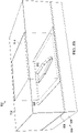
- FIG. 1 is a schematic diagram of an edge coupling device 100 similar to that described in C. Kopp, et al., "Silicon Photonic Circuits: On-CMOS Integration, Fiber Optical Coupling, and Packaging," Institute of Electrical and Electronics Engineers (IEEE) Journal of Selected Topics in Quantum Electronics, 2010 (Kopp ).
- the edge coupling device 100 is fabricated by covering an inverse-tapered single silicon waveguide 102 (e.g., silicon wire) on a silicon-on-insulator (SOI) wafer 104 with a silicon-rich oxide (SiOx). The SiOx is then partially etched to form a rib waveguide 106 whose refractive index is around 1.6.
- SOI silicon-on-insulator
- the mode size of the rib waveguide 106 is compatible for a coupling with a high-performance lensed fiber 108.
- the edge coupling device 100 is not integrated with any other photonic components, and there is no cladding material over the inverse-tapered single silicon wire 102 other than the SiOx waveguide 106.
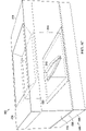
- FIG. 2 is a schematic diagram of another edge coupling device 200 similar to that described in United States Patent No. 7,738,753 entitled "CMOS Compatible Integrated Dielectric Optical Waveguide Coupler and Fabrication" to Solomon Assefa, et al.
- the edge coupling device 200 includes a silicon nitride (SiN) layer 202, a silicon dioxide (SiO 2 ) layer 204, and a Diamond Like Carbon (DLC) layer 206 stacked, in order, on top of the semiconductor device 208 having electronic and/or optoelectronic circuits fabricated thereon.
- SiN silicon nitride
- SiO 2 silicon dioxide
- DLC Diamond Like Carbon
- a silicon oxynitride (SiON) coupler 210 is disposed within a trench extending through the silicon dioxide layer 204 and the Diamond Like Carbon layer 206 and down to the silicon nitride layer 202.
- the edge coupling device 200 is fabricated without performing an etch process on a high-index material to form a ridge waveguide.
- the edge coupling device 200 may be integrated with other silicon photonic components, but the edge coupling device 200 is made in the process of making other silicon photonic components and is a part of the cladding material.
- edge coupling devices 100, 200 of FIG. 1-2 and other prior approaches suffer from various shortcomings in that inverse taper designs may suffer from limited mode size and difficulty with monolithically integrating the inverse taper designs with other photonic components.
- the embodiments provide for fabricating an edge coupling device by firstly removing cladding material on a fabricated silicon photonic wafer, by secondly filling the removed area with high-index material (e.g., material with a higher index than oxide), and thirdly etching the high-index material to form a ridge waveguide.
- the edge coupling device comprises an inversely tapered silicon waveguide covered by the high-index material.
- An optical mode may be transferred gradually from the silicon waveguide to the high-index material ridge waveguide as the width of the silicon waveguide narrows in the inverse taper.
- the final mode size of the edge coupling device may be mainly dependent on the size of the high-index material ridge waveguide. Fabrication of the edge coupling device does not negatively impact or influence the performance of components already fabricated on the silicon photonic wafer.
- the disclosed embodiments may provide for a larger mode size (e.g., about 3 ⁇ m to 5 ⁇ m) than a simple inverse taper, a low coupling loss, an improved reliability compared to a suspended edge coupler because there may be no suspended structure, an improved fabrication tolerance because the minimum inverse taper width may be larger, and monolithic integration with other passive and active SOI components.
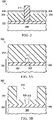
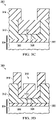
- FIGS. 3A-3D collectively illustrate an embodiment of a method of fabricating an edge coupling device 300, the end result of which is depicted in FIG. 3D .
- a representative portion of a die or integrated circuit wafer 302 is provided.
- the integrated circuit wafer 302 may include, for example, a PIC or integrated optical circuit.
- the PIC is a device that integrates multiple (at least two) photonic functions and as such is analogous to an electronic integrated circuit.
- the substrate 304 of the integrated circuit wafer 302 has a SOI structure as shown in FIG. 3A .
- SOI structure a layered semiconductor-insulator-semiconductor substrate is used place of a semiconductor only substrate in semiconductor manufacturing, especially microelectronics, to reduce parasitic device capacitance, thereby improving performance.
- a buried oxide (BOX) layer 306 is disposed between portions or layers of semiconductor material 308.
- the buried oxide layer 306 may comprise, for example, silicon dioxide or other suitable oxide.
- the buried oxide layer 306 is grown on the underlying semiconductor material 308.
- the BOX layer 306 may have a thickness ranging from about 40 nm to about 100 nm, depending on application.
- the semiconductor material 308 is, for example, silicon or a silicon-containing material.
- the semiconductor material 308 includes another elementary semiconductor, such as germanium and/or diamond.
- the semiconductor material 308 may also be a compound semiconductor including silicon carbide, gallium arsenic, gallium phosphide, indium phosphide, indium arsenide, and/or indium antimonide.
- the semiconductor material 308 may be an alloy semiconductor including silicon-germanium (SiGe), gallium arsenide phosphide (GaAsP), aluminum indium arsenide (AlInAs), aluminum gallium arsenide (AlGaAs), gallium indium arsenide (GaInAs), gallium indium phosphide (GaInP), and/or gallium indium arsenide phosphide (GaInAsP), or combinations thereof.
- the semiconductor material 308 comprises a group IV, a group III-V, or a group II-VI semiconductor material.
- the semiconductor material 308 may include a doped epitaxial layer, a gradient semiconductor layer, and/or a semiconductor layer overlying another semiconductor layer of a different type, such as a silicon layer on a silicon germanium layer.
- the semiconductor material 308 may be a p-type or an n-type depending on design requirements of the integrated circuit wafer 302.
- a portion of the semiconductor material 308 within the integrated circuit wafer 302 forms an inversely tapered waveguide 310.
- the inversely tapered waveguide 310 is utilized to propagate an optical signal through the integrated circuit wafer 302.
- the inversely tapered waveguide 310 has a dimension (e.g., width) that gradually diminishes as the inversely tapered waveguide approaches an edge or coupling junction of the integrated circuit wafer 302.
- the inversely tapered waveguide 310 may be formed using, for example, deep ultraviolet (DUV) lithography, reactive-ion etching (RIE), or other suitable techniques.
- the length of the taper in the inversely tapered waveguide 310 may vary depending on application and the mode size desired.
- the inversely tapered waveguide 310 is covered with cladding material 312.
- the cladding material 312 is formed from silicon dioxide. In an embodiment, more than 50% of the cladding material 312 is silicon dioxide.
- the thickness of the cladding material may be, for example, on the order of a few micrometers ( ⁇ m) (e.g., between about 1 ⁇ m and about 3 ⁇ m thick).
- the cladding material 312 may be formed by stacking layers of silicon dioxide, silicon nitride (Si 3 N 4 ), silicon carbide (SiC), or another suitable material.
- the cladding material 312 has a refractive index higher than that of oxide (e.g., the buried oxide 306).
- a portion of the cladding material 312 covering the inversely tapered waveguide 310 may be removed to form a trench 314.
- the trench 314 is disposed over, and vertically aligned with, the inversely tapered waveguide 310.
- the trench 314 is formed using a timed etch process.
- a buffered hydrofluoric acid (BHF) or other suitable etchant may be employed.
- BHF buffered hydrofluoric acid
- the cladding material 312 above a top surface of the inversely tapered waveguide 310 is removed. A slight over-etch or under-etch of the cladding material 312 due to inaccurate timing may be acceptable.
- a high-index material 316 is deposited as shown in FIG. 3C .
- the high-index material 316 is deposited where the cladding material 312 has previously been removed.
- the high-index material 316 is formed through any of a variety of deposition techniques, including, low-pressure chemical vapor deposition (LPCVD), atmospheric-pressure chemical vapor deposition (APCVD), plasma-enhanced chemical vapor deposition (PECVD), physical vapor deposition (PVD), sputtering, and future-developed deposition procedures.
- the high-index material 316 is deposited until the trench 314 has been at least partially filled.
- the high-index material 316 has a refractive index larger than the refractive index of silicon dioxide, which is about 1.445, but lower than the refractive index of silicon, which is about 3.5.
- the high-index material comprises silicon nitride, silicon oxide, silicon oxynitride, aluminum oxide (Al 2 O 3 ), aluminum nitride (AlN), or another suitable material.
- the thickness of the high-index material 316 may be in the range of 2 ⁇ m to 20 ⁇ m.
- the width of the trench 314 (e.g., the cladding removal area) may be greater than 50 ⁇ m to ensure the flatness and uniformity of the high-index material above the floor of the trench 314.
- a portion of the high-index material 316 is removed to generate a ridge waveguide 318 for the edge coupling device 300.
- a photolithography process is utilized to remove the high-index material 316.
- the high-index refractive material 316 is patterned to form the ridge waveguide 318.
- the ridge waveguide 318 is disposed over, and vertically aligned with, the inversely tapered silicon waveguide 310.
- the ridge waveguide 318 is disposed entirely within the trench 314.
- a portion of the ridge waveguide 318 protrudes at least partially from the trench 314.
- the ridge waveguide 318 is configured to work cooperatively with the inversely tapered silicon waveguide 310 to propagate the optical signal through the edge coupling device 300.
- the optical mode from the inversely tapered silicon waveguide 310 is gradually transferred to the ridge waveguide 318 as the width of the inversely tapered silicon waveguide 310 narrows.
- the mode size of the edge coupling device 300 is mainly dependent upon the mode size of the ridge waveguide 318.
- the mode size of the ridge waveguide 318 and/or the edge coupling device 300 is between about 3 ⁇ m and about 10 ⁇ m, which provides for a low coupling loss.
- the etch depth forming the ridge waveguide 318 is as deep as possible while still ensuring a single-mode condition of the ridge waveguide 318.
- the ridge waveguide 318 of the edge coupling device 300 is monolithically integrated with the substrate 304.
- FIGS. 4A-4D collectively illustrate an embodiment of a method of fabricating an edge coupling device 400, the end result of which is depicted in FIG. 4D .
- the method and corresponding elements 400-418 illustrated in FIGS. 4A-4D are similar to the method and elements 300-318 illustrated in FIGS. 3A-3D .
- an etch stop layer 420 has been included within the wafer 402.
- the etch stop layer 420 is deposited over the inversely tapered silicon waveguide 410 and a portion of the buried oxide layer 406 to protect those structures from the etchant used to form the trench 414 illustrated in FIG. 4B .
- the etch stop layer 420 comprises silicon oxide, silicon nitride, silicon carbide, silicon oxynitride, polysilicon, or combinations thereof. Due to the presence of the etch stop layer 420, etching may be performed until the etch stop layer 420 is reached instead of using a timed etch as described above. In other words, the etch stop layer 420 is used to control the end point during the etching processes. In an embodiment, the etch stop layer 420 is formed through any of a variety of deposition techniques, including, low-pressure chemical vapor deposition, atmospheric-pressure chemical vapor deposition, plasma-enhanced chemical vapor deposition, physical vapor deposition, sputtering, and future-developed deposition procedures. After etching, the high-index material 416 is deposited in the trench 414 and then patterned to form the ridge waveguide 418 as described above.
- FIGS. 5A-5D collectively illustrate an embodiment of a method of fabricating an edge coupling device 500, the end result of which is depicted in FIG. 5D .
- the method and elements 500-520 illustrated in FIGS. 5A-5D are similar to the method and elements 400-420 illustrated in FIGS. 4A-4D .
- the edge coupling device 500 in FIG. 5D is initially an unsuspended structure.
- a BOX layer 506 has been formed over a silicon semiconductor material 508 to form at least a portion of the substrate 504.
- the BOX layer 506 supports an inverse tapered silicon waveguide 510 covered by a silicon nitride etch stop layer 520.
- the silicon nitride etch stop layer 520 initially overlies the entire wafer 502. However, the silicon nitride disposed outside the intended area shown in FIG. 5A is removed by, for example, boiling phosphorus acid or by another suitable removal process. Thereafter, a layer of silicon dioxide cladding material 512 is disposed over the silicon nitride etch stop layer 520.
- a trench 514 having a width of approximately 400 ⁇ m is formed in the silicon dioxide cladding material 512 down to the etch stop layer 520 using a wet etch process. Thereafter, a silicon oxynitride or silicon oxide polymer layer 516 with a thickness of between about 3 ⁇ m to about 5 ⁇ m is deposited as shown in FIG. 5C . Then, the silicon oxynitride or silicon oxide polymer layer 516 is patterned to form the ridge waveguide 518 as shown in FIG. 5D .
- a central portion 522 of the ridge waveguide 518 has width of about 3 ⁇ m to about 5 ⁇ m while lateral portions 524 of the ridge waveguide 518, which are adjacent to the central portion 522, each have a width of about 200 ⁇ m.
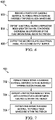
- FIG. 6 is a flowchart illustrating a method 600 of fabricating an edge coupling device according to an embodiment of the disclosure.
- the method 600 may commence, for example, after a PIC device with at least one inverse taper (e.g., an inversely tapered waveguide 310, 410, 510) covered by cladding material (e.g., cladding material 312, 412, 512) has been accepted for further processing or fabrication.
- a portion of the cladding material is removed to form a trench (e.g., trench 314, 414, 514) over the inversely tapered silicon waveguide.
- an etch stop layer e.g., etch stop layer 420, 520
- etching continues until the etch stop layer is reached. If an etch stop layer is not present, a timed etch may be performed.
- a material e.g., high refractive index material 316, 416, 516 having a refractive index greater than silicon dioxide is deposited over remaining portions of the cladding material and in the trench.
- a portion of the material within the trench is removed to form a ridge waveguide (e.g., ridge waveguide 318, 418, 518). While not shown or disclosed herein, it should be understood that further processing may thereafter take place as desired.
- FIG. 7 is a flowchart illustrating a method 700 of fabricating an edge coupling device according to an embodiment of the disclosure.
- the method 700 may commence, for example, after a PIC device with at least one inverse taper (e.g., an inversely tapered waveguide 310, 410, 510) covered by cladding material (e.g., cladding material 312, 412, 512) has been accepted for further processing or fabrication.
- a trench e.g., trench 314, 414, 514 is formed within a cladding material disposed over the inversely tapered silicon waveguide.
- the trench may be formed by etching down to the etch stop layer. If an etch stop layer is not present, the trench may be formed through a timed etch.
- a refractive index material (e.g., high refractive index material 316, 416, 515) is deposited within the trench.
- the refractive index material has a refractive index between about 1.445 and about 3.5.
- the refractive index material is patterned to form a ridge waveguide (e.g., ridge waveguide 318, 418, 518) within the trench. While not shown or disclosed herein, it should be understood that further processing may thereafter take place as desired.
- an optical mode may be transferred gradually from the silicon waveguide to the high-index material ridge waveguide as the width of the silicon waveguide narrows in the inverse taper.
- the final mode size of the edge coupling device may be mainly dependent on the size of the high-index material ridge waveguide. Fabrication of the edge coupling device does not negatively impact or influence the performance of components already fabricated on the silicon photonic wafer.
- the disclosed embodiments may provide for a larger mode size (e.g., 3 to 5 ⁇ m) than a simple inverse taper, a low coupling loss, an improved reliability compared to a suspended edge coupler because there may be no suspended structure, an improved fabrication tolerance because the minimum inverse taper width may be larger, and monolithic integration with other passive and active SOI components.
- a larger mode size e.g., 3 to 5 ⁇ m
- a simple inverse taper e.g., 3 to 5 ⁇ m
- a low coupling loss e.g., 3 to 5 ⁇ m
- an improved reliability compared to a suspended edge coupler because there may be no suspended structure
- an improved fabrication tolerance because the minimum inverse taper width may be larger
- monolithic integration with other passive and active SOI components e.g., 3 to 5 ⁇ m
Landscapes
- Physics & Mathematics (AREA)
- General Physics & Mathematics (AREA)
- Optics & Photonics (AREA)
- Engineering & Computer Science (AREA)
- Microelectronics & Electronic Packaging (AREA)
- Optical Integrated Circuits (AREA)
Description
- In optical transceivers, it is desirable to integrate as many photonic components in one chip as possible. As integration density increases and the sizes of photonic components shrink, however, it is increasingly difficult to integrate the photonic integrated circuit (PIC) with other optical components such as fibers because the mode size in the waveguide of the PIC shrinks correspondingly. For example, the mode size of a typical 450 nanometer (nm) x 220 nm waveguide in a silicon photonic based PIC is roughly the size of the waveguide itself, but the mode size (e.g., mode field diameter) of a standard single mode fiber is as large as 9.2 micrometers (µm). Thus, the mode size of the waveguide on the PIC is much larger than the mode size of the fiber.
- Lenses may be used to reduce the mode size of the fiber to correspond to the mode size of the waveguide of the PIC. However, packaging the PIC with lens and fiber is challenging due to the limited alignment tolerance if the mode size at the interface of the PIC is too small.
- A mode converter may, for an edge coupled PIC, be used to enlarge the mode size of the waveguide of the PIC. However, the mode converter should be able to be integrated with other components on the PIC as well.
-
US 2005/123244A discloses awaveguide coupler 100 integrated on a substrate 110 to interconnect a large waveguide 120 and a small waveguide 130. The large waveguide 120 has a solid section to receive and guide an input optical beam 101 and a hollow section in which at least a part of the small waveguide 130 is embedded. - The present invention is as defined in the appended independent claims. In one embodiment, the disclosure includes a method of fabricating an edge coupling device. The method includes removing a portion of cladding material to form a trench over an inversely tapered silicon waveguide, depositing a material having a refractive index greater than silicon dioxide over remaining portions of the cladding material and in the trench, and removing a portion of the material within the trench to form a ridge waveguide
- In one embodiment, the disclosure includes a method of fabricating an edge coupling device. The method includes forming a trench within a cladding material disposed over an inversely tapered silicon waveguide, depositing a refractive index material within the trench, wherein the refractive index material has a refractive index between 1.445 and 3.5, and patterning the refractive index material to form a ridge waveguide within the trench.
- In another embodiment, the disclosure includes edge coupling device. The edge coupling device includes a substrate, a buried oxide disposed over the substrate, a cladding material disposed over the buried oxide, wherein the cladding material includes a trench, an inversely tapered silicon waveguide disposed within the cladding material beneath the trench, and a ridge waveguide disposed within the trench, wherein the ridge waveguide and the inversely tapered silicon waveguide are vertically-aligned with each other.
-
-
FIG. 1 is a schematic diagram of an edge coupling device. -
FIG. 2 is a schematic diagram of another edge coupling device. -
FIGS. 3A-3D collectively illustrate an embodiment of a method of fabricating an edge coupling device; -
FIGS. 4A-4D collectively illustrate an embodiment of a method of fabricating an edge coupling device; -
FIGS. 5A-5D collectively illustrate an embodiment of another method of fabricating an edge coupling device; -
FIG. 6 is a flowchart illustrating a method of fabricating an edge coupling device according to an embodiment of the disclosure; -
FIG. 7 is a flowchart illustrating a method of fabricating an edge coupling device according to an embodiment of the disclosure. - It should be understood at the outset that, although illustrative implementations of one or more embodiments are provided below, the disclosed systems and/or methods may be implemented using any number of techniques, whether currently known or in existence. The disclosure should in no way be limited to the illustrative implementations, drawings, and techniques illustrated below, including the exemplary designs and implementations illustrated and described herein, but may be modified within the scope of the appended claims.
-
FIG. 1 is a schematic diagram of anedge coupling device 100 similar to that described in C. Kopp, et al., "Silicon Photonic Circuits: On-CMOS Integration, Fiber Optical Coupling, and Packaging," Institute of Electrical and Electronics Engineers (IEEE) Journal of Selected Topics in Quantum Electronics, 2010 (Kopp). Theedge coupling device 100 is fabricated by covering an inverse-tapered single silicon waveguide 102 (e.g., silicon wire) on a silicon-on-insulator (SOI) wafer 104 with a silicon-rich oxide (SiOx). The SiOx is then partially etched to form arib waveguide 106 whose refractive index is around 1.6. The mode size of therib waveguide 106 is compatible for a coupling with a high-performance lensedfiber 108. However, theedge coupling device 100 is not integrated with any other photonic components, and there is no cladding material over the inverse-taperedsingle silicon wire 102 other than the SiOxwaveguide 106. -
FIG. 2 is a schematic diagram of anotheredge coupling device 200 similar to that described inUnited States Patent No. 7,738,753 entitled "CMOS Compatible Integrated Dielectric Optical Waveguide Coupler and Fabrication" to Solomon Assefa, et al. As shown, theedge coupling device 200 includes a silicon nitride (SiN)layer 202, a silicon dioxide (SiO2)layer 204, and a Diamond Like Carbon (DLC)layer 206 stacked, in order, on top of thesemiconductor device 208 having electronic and/or optoelectronic circuits fabricated thereon. A silicon oxynitride (SiON)coupler 210 is disposed within a trench extending through thesilicon dioxide layer 204 and the Diamond LikeCarbon layer 206 and down to thesilicon nitride layer 202. However, theedge coupling device 200 is fabricated without performing an etch process on a high-index material to form a ridge waveguide. Theedge coupling device 200 may be integrated with other silicon photonic components, but theedge coupling device 200 is made in the process of making other silicon photonic components and is a part of the cladding material. - Unfortunately, the
edge coupling devices FIG. 1-2 and other prior approaches suffer from various shortcomings in that inverse taper designs may suffer from limited mode size and difficulty with monolithically integrating the inverse taper designs with other photonic components. - Disclosed herein are embodiments for addressing some of the issues noted above. As will be more fully explained below, the embodiments provide for fabricating an edge coupling device by firstly removing cladding material on a fabricated silicon photonic wafer, by secondly filling the removed area with high-index material (e.g., material with a higher index than oxide), and thirdly etching the high-index material to form a ridge waveguide. The edge coupling device comprises an inversely tapered silicon waveguide covered by the high-index material. An optical mode may be transferred gradually from the silicon waveguide to the high-index material ridge waveguide as the width of the silicon waveguide narrows in the inverse taper. The final mode size of the edge coupling device may be mainly dependent on the size of the high-index material ridge waveguide. Fabrication of the edge coupling device does not negatively impact or influence the performance of components already fabricated on the silicon photonic wafer. The disclosed embodiments may provide for a larger mode size (e.g., about 3 µm to 5 µm) than a simple inverse taper, a low coupling loss, an improved reliability compared to a suspended edge coupler because there may be no suspended structure, an improved fabrication tolerance because the minimum inverse taper width may be larger, and monolithic integration with other passive and active SOI components.
-
FIGS. 3A-3D collectively illustrate an embodiment of a method of fabricating anedge coupling device 300, the end result of which is depicted inFIG. 3D . As shown inFIG. 3A , a representative portion of a die orintegrated circuit wafer 302 is provided. Theintegrated circuit wafer 302 may include, for example, a PIC or integrated optical circuit. The PIC is a device that integrates multiple (at least two) photonic functions and as such is analogous to an electronic integrated circuit. - In an embodiment, the
substrate 304 of theintegrated circuit wafer 302 has a SOI structure as shown inFIG. 3A . In the SOI structure, a layered semiconductor-insulator-semiconductor substrate is used place of a semiconductor only substrate in semiconductor manufacturing, especially microelectronics, to reduce parasitic device capacitance, thereby improving performance. In thesubstrate 304 ofFIG. 3A , a buried oxide (BOX)layer 306 is disposed between portions or layers ofsemiconductor material 308. The buriedoxide layer 306 may comprise, for example, silicon dioxide or other suitable oxide. In an embodiment, the buriedoxide layer 306 is grown on theunderlying semiconductor material 308. TheBOX layer 306 may have a thickness ranging from about 40 nm to about 100 nm, depending on application. - In an embodiment, the
semiconductor material 308 is, for example, silicon or a silicon-containing material. Alternatively or additionally, thesemiconductor material 308 includes another elementary semiconductor, such as germanium and/or diamond. Thesemiconductor material 308 may also be a compound semiconductor including silicon carbide, gallium arsenic, gallium phosphide, indium phosphide, indium arsenide, and/or indium antimonide. Thesemiconductor material 308 may be an alloy semiconductor including silicon-germanium (SiGe), gallium arsenide phosphide (GaAsP), aluminum indium arsenide (AlInAs), aluminum gallium arsenide (AlGaAs), gallium indium arsenide (GaInAs), gallium indium phosphide (GaInP), and/or gallium indium arsenide phosphide (GaInAsP), or combinations thereof. In an embodiment, thesemiconductor material 308 comprises a group IV, a group III-V, or a group II-VI semiconductor material. - The
semiconductor material 308 may include a doped epitaxial layer, a gradient semiconductor layer, and/or a semiconductor layer overlying another semiconductor layer of a different type, such as a silicon layer on a silicon germanium layer. Thesemiconductor material 308 may be a p-type or an n-type depending on design requirements of theintegrated circuit wafer 302. - As shown in
FIG. 3A , a portion of thesemiconductor material 308 within theintegrated circuit wafer 302 forms an inversely taperedwaveguide 310. The inversely taperedwaveguide 310 is utilized to propagate an optical signal through theintegrated circuit wafer 302. The inversely taperedwaveguide 310 has a dimension (e.g., width) that gradually diminishes as the inversely tapered waveguide approaches an edge or coupling junction of theintegrated circuit wafer 302. The inversely taperedwaveguide 310 may be formed using, for example, deep ultraviolet (DUV) lithography, reactive-ion etching (RIE), or other suitable techniques. The length of the taper in the inversely taperedwaveguide 310 may vary depending on application and the mode size desired. - The inversely tapered
waveguide 310 is covered withcladding material 312. In an embodiment, thecladding material 312 is formed from silicon dioxide. In an embodiment, more than 50% of thecladding material 312 is silicon dioxide. The thickness of the cladding material may be, for example, on the order of a few micrometers (µm) (e.g., between about 1 µm and about 3 µm thick). In an embodiment, thecladding material 312 may be formed by stacking layers of silicon dioxide, silicon nitride (Si3N4), silicon carbide (SiC), or another suitable material. In an embodiment, thecladding material 312 has a refractive index higher than that of oxide (e.g., the buried oxide 306). - As shown in
FIG. 3B , a portion of thecladding material 312 covering the inversely taperedwaveguide 310 may be removed to form atrench 314. As shown, thetrench 314 is disposed over, and vertically aligned with, the inversely taperedwaveguide 310. In an embodiment, thetrench 314 is formed using a timed etch process. A buffered hydrofluoric acid (BHF) or other suitable etchant may be employed. Using the timed etch process, thecladding material 312 above a top surface of the inversely taperedwaveguide 310 is removed. A slight over-etch or under-etch of thecladding material 312 due to inaccurate timing may be acceptable. - After the
trench 314 has been formed in thecladding material 312, a high-index material 316 is deposited as shown inFIG. 3C . In other words, the high-index material 316 is deposited where thecladding material 312 has previously been removed. In an embodiment, the high-index material 316 is formed through any of a variety of deposition techniques, including, low-pressure chemical vapor deposition (LPCVD), atmospheric-pressure chemical vapor deposition (APCVD), plasma-enhanced chemical vapor deposition (PECVD), physical vapor deposition (PVD), sputtering, and future-developed deposition procedures. - In an embodiment, the high-
index material 316 is deposited until thetrench 314 has been at least partially filled. The high-index material 316 has a refractive index larger than the refractive index of silicon dioxide, which is about 1.445, but lower than the refractive index of silicon, which is about 3.5. In an embodiment, the high-index material comprises silicon nitride, silicon oxide, silicon oxynitride, aluminum oxide (Al2O3), aluminum nitride (AlN), or another suitable material. The thickness of the high-index material 316 may be in the range of 2 µm to 20 µm. The width of the trench 314 (e.g., the cladding removal area) may be greater than 50 µm to ensure the flatness and uniformity of the high-index material above the floor of thetrench 314. - As shown in
FIG. 3D , a portion of the high-index material 316 is removed to generate aridge waveguide 318 for theedge coupling device 300. In an embodiment, a photolithography process is utilized to remove the high-index material 316. In other words, the high-indexrefractive material 316 is patterned to form theridge waveguide 318. As shown, theridge waveguide 318 is disposed over, and vertically aligned with, the inversely taperedsilicon waveguide 310. In an embodiment, theridge waveguide 318 is disposed entirely within thetrench 314. In another embodiment, a portion of theridge waveguide 318 protrudes at least partially from thetrench 314. - The
ridge waveguide 318 is configured to work cooperatively with the inversely taperedsilicon waveguide 310 to propagate the optical signal through theedge coupling device 300. For example, the optical mode from the inversely taperedsilicon waveguide 310 is gradually transferred to theridge waveguide 318 as the width of the inversely taperedsilicon waveguide 310 narrows. The mode size of theedge coupling device 300 is mainly dependent upon the mode size of theridge waveguide 318. In an embodiment, the mode size of theridge waveguide 318 and/or theedge coupling device 300 is between about 3 µm and about 10 µm, which provides for a low coupling loss. In an embodiment, the etch depth forming theridge waveguide 318 is as deep as possible while still ensuring a single-mode condition of theridge waveguide 318. Theridge waveguide 318 of theedge coupling device 300 is monolithically integrated with thesubstrate 304. -
FIGS. 4A-4D collectively illustrate an embodiment of a method of fabricating anedge coupling device 400, the end result of which is depicted inFIG. 4D . The method and corresponding elements 400-418 illustrated inFIGS. 4A-4D are similar to the method and elements 300-318 illustrated inFIGS. 3A-3D . However, in the method depicted inFIGS. 4A-4D anetch stop layer 420 has been included within thewafer 402. Theetch stop layer 420 is deposited over the inversely taperedsilicon waveguide 410 and a portion of the buriedoxide layer 406 to protect those structures from the etchant used to form thetrench 414 illustrated inFIG. 4B . In an embodiment, theetch stop layer 420 comprises silicon oxide, silicon nitride, silicon carbide, silicon oxynitride, polysilicon, or combinations thereof. Due to the presence of theetch stop layer 420, etching may be performed until theetch stop layer 420 is reached instead of using a timed etch as described above. In other words, theetch stop layer 420 is used to control the end point during the etching processes. In an embodiment, theetch stop layer 420 is formed through any of a variety of deposition techniques, including, low-pressure chemical vapor deposition, atmospheric-pressure chemical vapor deposition, plasma-enhanced chemical vapor deposition, physical vapor deposition, sputtering, and future-developed deposition procedures. After etching, the high-index material 416 is deposited in thetrench 414 and then patterned to form theridge waveguide 418 as described above. -
FIGS. 5A-5D collectively illustrate an embodiment of a method of fabricating anedge coupling device 500, the end result of which is depicted inFIG. 5D . The method and elements 500-520 illustrated inFIGS. 5A-5D are similar to the method and elements 400-420 illustrated inFIGS. 4A-4D . However, theedge coupling device 500 inFIG. 5D is initially an unsuspended structure. - As shown in
FIG. 5A , aBOX layer 506 has been formed over asilicon semiconductor material 508 to form at least a portion of thesubstrate 504. TheBOX layer 506 supports an inversetapered silicon waveguide 510 covered by a silicon nitrideetch stop layer 520. In an embodiment, the silicon nitrideetch stop layer 520 initially overlies theentire wafer 502. However, the silicon nitride disposed outside the intended area shown inFIG. 5A is removed by, for example, boiling phosphorus acid or by another suitable removal process. Thereafter, a layer of silicondioxide cladding material 512 is disposed over the silicon nitrideetch stop layer 520. - Turning to
FIG. 5B , atrench 514 having a width of approximately 400 µm is formed in the silicondioxide cladding material 512 down to theetch stop layer 520 using a wet etch process. Thereafter, a silicon oxynitride or siliconoxide polymer layer 516 with a thickness of between about 3 µm to about 5 µm is deposited as shown inFIG. 5C . Then, the silicon oxynitride or siliconoxide polymer layer 516 is patterned to form theridge waveguide 518 as shown inFIG. 5D . In an embodiment, acentral portion 522 of theridge waveguide 518 has width of about 3 µm to about 5 µm whilelateral portions 524 of theridge waveguide 518, which are adjacent to thecentral portion 522, each have a width of about 200 µm. -
FIG. 6 is a flowchart illustrating amethod 600 of fabricating an edge coupling device according to an embodiment of the disclosure. Themethod 600 may commence, for example, after a PIC device with at least one inverse taper (e.g., an inversely taperedwaveguide cladding material block 602, a portion of the cladding material is removed to form a trench (e.g.,trench etch stop layer 420, 520) is included in the PIC device, etching continues until the etch stop layer is reached. If an etch stop layer is not present, a timed etch may be performed. - In
block 604, a material (e.g., highrefractive index material block 606, a portion of the material within the trench is removed to form a ridge waveguide (e.g.,ridge waveguide -
FIG. 7 is a flowchart illustrating amethod 700 of fabricating an edge coupling device according to an embodiment of the disclosure. Themethod 700 may commence, for example, after a PIC device with at least one inverse taper (e.g., an inversely taperedwaveguide cladding material block 702, a trench (e.g.,trench etch stop layer 420, 520) is included in the PIC device, the trench may be formed by etching down to the etch stop layer. If an etch stop layer is not present, the trench may be formed through a timed etch. - In
block 704, a refractive index material (e.g., highrefractive index material block 706, the refractive index material is patterned to form a ridge waveguide (e.g.,ridge waveguide - Based on the embodiments disclosed herein, one skilled in the art will appreciate that an optical mode may be transferred gradually from the silicon waveguide to the high-index material ridge waveguide as the width of the silicon waveguide narrows in the inverse taper. The final mode size of the edge coupling device may be mainly dependent on the size of the high-index material ridge waveguide. Fabrication of the edge coupling device does not negatively impact or influence the performance of components already fabricated on the silicon photonic wafer. The disclosed embodiments may provide for a larger mode size (e.g., 3 to 5 µm) than a simple inverse taper, a low coupling loss, an improved reliability compared to a suspended edge coupler because there may be no suspended structure, an improved fabrication tolerance because the minimum inverse taper width may be larger, and monolithic integration with other passive and active SOI components.
- While several embodiments have been provided in the present disclosure, it should be understood that the disclosed systems and methods might be embodied in many other specific forms without departing from the scope of the present disclosure. The present examples are to be considered as illustrative and not restrictive, and the intention is not to be limited to the details given herein.
- Other examples of changes, substitutions, and alterations are ascertainable by one skilled in the art and could be made without departing from the scope disclosed herein.
Claims (12)
- A method of fabricating an edge coupling device, comprising:removing a portion of cladding material (312), wherein the cladding material comprises silicon dioxide, to form a trench (314) over an inversely tapered silicon waveguide (310); wherein the inversely tapered silicon waveguide is covered with the cladding material;depositing a high-index material (316) having a refractive index, which is greater than a refractive index of silicon dioxide and less than a refractive index of silicon, over remaining portions of the cladding material and in the trench; andremoving a portion of the high-index material within the trench to form a ridge waveguide (318), vertically aligned with the inversely tapered silicon waveguide.
- The method of claim 1, further comprising forming an etch stop layer (420) over the inversely tapered silicon waveguide prior to removing the portion of the cladding material, and wherein the portion of the cladding material is removed by etching down to the etch stop layer.
- The method of claim 2, further comprising removing the portion of the cladding material using a timed etch process.
- The method of claim 1, further comprising removing the portion of the material within the trench using a photolithography process.
- The method of claim 1, wherein the cladding material comprises a silicon dioxide layer and at least one of silicon nitride layer and a silicon carbide layer.
- The method of claim 1, wherein the high-index material is one of silicon nitride (SiN), silicon oxide (SiOx), silicon oxynitride (SiON), aluminum oxide (Al2O3), and aluminum nitride (AlN).
- 2 The method of claim 1, wherein a thickness of the high-index material is between 2 micrometers (µm) and 20 µm.
- The method of claim 1, wherein a width of the trench is greater than a width of the inversely tapered silicon waveguide, and wherein the width of the trench is greater than 5 µm.
- The method of claim 1, wherein the ridge waveguide has a single-mode condition, and wherein the mode size is between 3 micrometers (µm) and 10 µm.
- The method of claim 1, wherein the ridge waveguide is formed such that a ridge waveguide width is equivalent to a ridge waveguide height.
- An edge coupling device comprising:a substrate (304);a buried oxide (306) disposed over the substrate;a cladding material (312) disposed over the buried oxide, wherein the cladding material includes a trench;an inversely tapered silicon waveguide (310) disposed within the cladding material beneath the trench; anda ridge waveguide (318) disposed within the trench, wherein the ridge waveguide and the inversely tapered silicon waveguide are vertically-aligned with each other, wherein a high-index material (316) having a refractive index, which is greater than a refractive index of silicon dioxide and less than a refractive index of silicon,is patterned to form the ridge waveguide.
- The edge coupling device of claim 11,
wherein more than 50% of the cladding material is silicon dioxide (SiO2), wherein the cladding material comprises multiple stacks comprising at least one of silicon nitride (SiN) and silicon carbide (SiC), and wherein the cladding material has a thickness of between 1 micrometer (µm) and 3 µm.
Applications Claiming Priority (2)
| Application Number | Priority Date | Filing Date | Title |
|---|---|---|---|
| US201461977366P | 2014-04-09 | 2014-04-09 | |
| PCT/US2015/024765 WO2015157323A1 (en) | 2014-04-09 | 2015-04-07 | Edge coupling device fabrication |
Publications (2)
| Publication Number | Publication Date |
|---|---|
| EP3116825A1 EP3116825A1 (en) | 2017-01-18 |
| EP3116825B1 true EP3116825B1 (en) | 2022-06-15 |
Family
ID=52875349
Family Applications (1)
| Application Number | Title | Priority Date | Filing Date |
|---|---|---|---|
| EP15716708.1A Active EP3116825B1 (en) | 2014-04-09 | 2015-04-07 | Edge coupling device fabrication |
Country Status (6)
| Country | Link |
|---|---|
| US (2) | US9703039B2 (en) |
| EP (1) | EP3116825B1 (en) |
| JP (1) | JP6314354B2 (en) |
| KR (1) | KR20160139022A (en) |
| CN (1) | CN106164722B (en) |
| WO (1) | WO2015157323A1 (en) |
Families Citing this family (16)
| Publication number | Priority date | Publication date | Assignee | Title |
|---|---|---|---|---|
| US9678273B2 (en) * | 2015-06-01 | 2017-06-13 | International Business Machines Corporation | Device for propagating light and method for fabricating a device |
| US9658400B2 (en) | 2015-06-01 | 2017-05-23 | International Business Machines Corporation | Method for fabricating a device for propagating light |
| CN107329208B (en) * | 2017-07-10 | 2023-05-09 | 熠谱(上海)半导体制造有限公司 | Silicon photon spot-size converter with gradient change of refractive index |
| JP6930378B2 (en) * | 2017-10-31 | 2021-09-01 | 日本電信電話株式会社 | Semiconductor laser |
| JP6946936B2 (en) * | 2017-10-31 | 2021-10-13 | 日本電信電話株式会社 | Optical waveguide and its manufacturing method |
| US11131601B2 (en) * | 2017-11-30 | 2021-09-28 | Rain Tree Photonics Pte. Ltd. | Method for in-line optical testing |
| US11353659B2 (en) | 2019-03-29 | 2022-06-07 | Rochester Institute Of Technology | Photonic chip features for fiber attachment |
| US11169328B2 (en) * | 2019-09-20 | 2021-11-09 | Taiwan Semiconductor Manufacturing Co., Ltd. | Photonic structure and method for forming the same |
| CN111239899B (en) * | 2020-03-17 | 2022-08-09 | 联合微电子中心有限责任公司 | Method for realizing spot size conversion based on substrate SiON waveguide bonding and spot size converter |
| EP4020027A1 (en) * | 2020-12-23 | 2022-06-29 | EFFECT Photonics B.V. | An environmentally protected photonic integrated circuit |
| EP4278224A4 (en) | 2021-01-18 | 2024-12-18 | Aayuna Inc. | Dual layer optical coupling configuration between photonic integrated circuit and external single mode optical fiber |
| US11971572B2 (en) * | 2022-02-18 | 2024-04-30 | Globalfoundries U.S. Inc. | Optical waveguide with stacked cladding material layers |
| CN115598764B (en) * | 2022-11-28 | 2023-03-14 | 之江实验室 | End face coupler, optoelectronic chip and manufacturing method of end face coupler |
| GB2636078B (en) * | 2023-11-23 | 2026-04-08 | Ligentec Sa | Photonic Integrated Circuit |
| CN117492138B (en) * | 2023-12-29 | 2024-04-09 | 光本位科技(苏州)有限公司 | Heterogeneous integration method and structure of phase change optical device and optical waveguide platform |
| CN119738985B (en) * | 2024-12-18 | 2025-09-26 | 甬江实验室 | Preparation method of inverted structure film lithium niobate/lithium tantalate electro-optic modulator |
Citations (2)
| Publication number | Priority date | Publication date | Assignee | Title |
|---|---|---|---|---|
| US20050123244A1 (en) * | 2003-12-03 | 2005-06-09 | Block Bruce A. | Embedded optical waveguide coupler |
| US20080290066A1 (en) * | 2007-05-24 | 2008-11-27 | Lumera Corporation | Method of Fabricating Polymer Modulators With Etch Stop Clads |
Family Cites Families (27)
| Publication number | Priority date | Publication date | Assignee | Title |
|---|---|---|---|---|
| JPS61204921A (en) | 1985-03-08 | 1986-09-11 | 松下電器産業株式会社 | Molding method for laminated ceramic elements |
| JPH0415605A (en) * | 1990-05-09 | 1992-01-21 | Oki Electric Ind Co Ltd | Optical waveguide |
| US5585957A (en) * | 1993-03-25 | 1996-12-17 | Nippon Telegraph And Telephone Corporation | Method for producing various semiconductor optical devices of differing optical characteristics |
| JPH07168146A (en) * | 1993-04-07 | 1995-07-04 | Nippon Telegr & Teleph Corp <Ntt> | Spot conversion optical waveguide |
| JPH08330671A (en) * | 1995-05-31 | 1996-12-13 | Hitachi Ltd | Semiconductor optical device |
| JP3957187B2 (en) * | 2002-10-23 | 2007-08-15 | 日本電信電話株式会社 | Variable optical attenuator |
| US6954568B2 (en) * | 2003-04-29 | 2005-10-11 | Intel Corporation | Method and apparatus for splitting or combining optical beams with A Y coupler with reduced loss and electrical isolation |
| DK1706767T3 (en) * | 2003-12-29 | 2019-07-22 | Google Llc | OPTOCUCLER DEVICE |
| CN1271765C (en) * | 2004-04-02 | 2006-08-23 | 华中科技大学 | Ridge waveguide polarized don't-care semiconductor optical enlarger of integrated modular spot converter |
| US20060133754A1 (en) * | 2004-12-21 | 2006-06-22 | Vipulkumar Patel | Ultra low-loss CMOS compatible silicon waveguides |
| US7668416B2 (en) * | 2006-06-05 | 2010-02-23 | Bing Li | Single mode photonic circuit architecture and a new optical splitter design based on parallel waveguide mode conversion |
| JP5082414B2 (en) * | 2006-12-06 | 2012-11-28 | 株式会社日立製作所 | Optical semiconductor device and optical waveguide device |
| US8285092B2 (en) * | 2007-03-20 | 2012-10-09 | Nec Corporation | Optical waveguide and spot size converter using the same |
| DE102008012859B4 (en) * | 2007-12-21 | 2023-10-05 | OSRAM Opto Semiconductors Gesellschaft mit beschränkter Haftung | Laser light source with a filter structure |
| US7738753B2 (en) | 2008-06-30 | 2010-06-15 | International Business Machines Corporation | CMOS compatible integrated dielectric optical waveguide coupler and fabrication |
| US7643710B1 (en) * | 2008-09-17 | 2010-01-05 | Intel Corporation | Method and apparatus for efficient coupling between silicon photonic chip and optical fiber |
| JP5386254B2 (en) * | 2009-07-15 | 2014-01-15 | 株式会社フジクラ | Optical element having spot size conversion optical waveguide |
| CN102033264A (en) * | 2009-09-25 | 2011-04-27 | 中国科学院半导体研究所 | Manufacturing method of ridge-shaped optical waveguide and inverted-cone coupler assembly |
| US9158175B2 (en) * | 2010-01-27 | 2015-10-13 | K G Technology Associates, Inc. | Optical coupler |
| JP5764776B2 (en) | 2010-10-08 | 2015-08-19 | 国立研究開発法人産業技術総合研究所 | Optical conversion element |
| US20120214017A1 (en) | 2011-02-22 | 2012-08-23 | Pourin Welding Engineering Co., Ltd. | Weld Overlay Structure and a Method of Providing a Weld Overlay Structure |
| US8410566B2 (en) * | 2011-07-21 | 2013-04-02 | Kotura, Inc. | Application of electrical field power to light-transmitting medium |
| KR20130069146A (en) * | 2011-12-16 | 2013-06-26 | 한국전자통신연구원 | Optical coupling devices and silicon photonics chips having the same |
| US9036956B2 (en) * | 2012-02-17 | 2015-05-19 | Haynes and Boone, LLP | Method of fabricating a polymer waveguide |
| KR20130112548A (en) * | 2012-04-04 | 2013-10-14 | 한국전자통신연구원 | Spot size converter and manufacturing method of the same |
| US9091806B2 (en) * | 2012-04-05 | 2015-07-28 | Oracle International Corporation | Surface-normal optical coupling using a holographic recording material |
| JP2014038183A (en) * | 2012-08-15 | 2014-02-27 | National Institute Of Advanced Industrial & Technology | Optical waveguide, and manufacturing method thereof |
-
2015
- 2015-04-07 CN CN201580018130.0A patent/CN106164722B/en active Active
- 2015-04-07 WO PCT/US2015/024765 patent/WO2015157323A1/en not_active Ceased
- 2015-04-07 JP JP2016561653A patent/JP6314354B2/en active Active
- 2015-04-07 EP EP15716708.1A patent/EP3116825B1/en active Active
- 2015-04-07 KR KR1020167030248A patent/KR20160139022A/en not_active Ceased
- 2015-04-07 US US14/680,917 patent/US9703039B2/en active Active
-
2017
- 2017-04-19 US US15/491,772 patent/US10197733B2/en active Active
Patent Citations (2)
| Publication number | Priority date | Publication date | Assignee | Title |
|---|---|---|---|---|
| US20050123244A1 (en) * | 2003-12-03 | 2005-06-09 | Block Bruce A. | Embedded optical waveguide coupler |
| US20080290066A1 (en) * | 2007-05-24 | 2008-11-27 | Lumera Corporation | Method of Fabricating Polymer Modulators With Etch Stop Clads |
Also Published As
| Publication number | Publication date |
|---|---|
| US9703039B2 (en) | 2017-07-11 |
| JP2017514167A (en) | 2017-06-01 |
| KR20160139022A (en) | 2016-12-06 |
| US10197733B2 (en) | 2019-02-05 |
| JP6314354B2 (en) | 2018-04-25 |
| CN106164722B (en) | 2020-06-02 |
| US20150293303A1 (en) | 2015-10-15 |
| US20170219777A1 (en) | 2017-08-03 |
| WO2015157323A1 (en) | 2015-10-15 |
| CN106164722A (en) | 2016-11-23 |
| EP3116825A1 (en) | 2017-01-18 |
Similar Documents
| Publication | Publication Date | Title |
|---|---|---|
| US10197733B2 (en) | Edge coupling device fabrication | |
| US10643903B2 (en) | Mode converter and method of fabricating thereof | |
| US8000565B2 (en) | Buried dual taper waveguide for passive alignment and photonic integration | |
| WO2016195732A1 (en) | Back end of line process integrated optical device fabrication | |
| US10317623B2 (en) | Back end of line process integrated optical device fabrication | |
| US10416381B1 (en) | Spot-size-converter design for facet optical coupling | |
| WO2013033252A1 (en) | Integrated waveguide coupler | |
| WO2015168419A1 (en) | Inverse taper waveguides for low-loss mode converters | |
| KR20150113095A (en) | Photonic device structure and method of manufacture | |
| US10096971B2 (en) | Hybrid semiconductor lasers | |
| US11966078B2 (en) | Optoelectronic device and method of manufacture thereof | |
| CN108718534A (en) | Integrating v-grooves on silicon-on-insulator wafers for direct fiber coupling | |
| US12044908B2 (en) | III-V/SI hybrid optoelectronic device and method of manufacture | |
| US20120251034A1 (en) | Monolithic integration of dielectric waveguides and germanium-based devices | |
| US10746925B2 (en) | Silicon nitride grating couplers | |
| US9709748B2 (en) | Frontside coupled waveguide with backside optical connection using a curved spacer | |
| EP4394464A1 (en) | Structure with substrate-embedded arrow waveguide and method | |
| EP3840044A1 (en) | Substrate and method for monolithic integration of electronic and optoelectronic devices | |
| CN117120899A (en) | Method for manufacturing a photonic device having at least two photonic chips and photonic device |
Legal Events
| Date | Code | Title | Description |
|---|---|---|---|
| STAA | Information on the status of an ep patent application or granted ep patent |
Free format text: STATUS: THE INTERNATIONAL PUBLICATION HAS BEEN MADE |
|
| PUAI | Public reference made under article 153(3) epc to a published international application that has entered the european phase |
Free format text: ORIGINAL CODE: 0009012 |
|
| STAA | Information on the status of an ep patent application or granted ep patent |
Free format text: STATUS: REQUEST FOR EXAMINATION WAS MADE |
|
| 17P | Request for examination filed |
Effective date: 20161010 |
|
| AK | Designated contracting states |
Kind code of ref document: A1 Designated state(s): AL AT BE BG CH CY CZ DE DK EE ES FI FR GB GR HR HU IE IS IT LI LT LU LV MC MK MT NL NO PL PT RO RS SE SI SK SM TR |
|
| AX | Request for extension of the european patent |
Extension state: BA ME |
|
| RIN1 | Information on inventor provided before grant (corrected) |
Inventor name: PAN, HUAPU Inventor name: CHEN, HONGMIN Inventor name: LIU, ZONGRONG Inventor name: WEI, HONGZHEN |
|
| DAV | Request for validation of the european patent (deleted) | ||
| DAX | Request for extension of the european patent (deleted) | ||
| STAA | Information on the status of an ep patent application or granted ep patent |
Free format text: STATUS: EXAMINATION IS IN PROGRESS |
|
| 17Q | First examination report despatched |
Effective date: 20191202 |
|
| RIC1 | Information provided on ipc code assigned before grant |
Ipc: G02B 6/132 20060101ALI20211215BHEP Ipc: G02B 6/30 20060101ALI20211215BHEP Ipc: G02B 6/122 20060101ALI20211215BHEP Ipc: G02B 6/136 20060101ALI20211215BHEP Ipc: G02B 6/12 20060101ALI20211215BHEP Ipc: B82Y 20/00 20110101AFI20211215BHEP |
|
| GRAP | Despatch of communication of intention to grant a patent |
Free format text: ORIGINAL CODE: EPIDOSNIGR1 |
|
| STAA | Information on the status of an ep patent application or granted ep patent |
Free format text: STATUS: GRANT OF PATENT IS INTENDED |
|
| INTG | Intention to grant announced |
Effective date: 20220224 |
|
| GRAS | Grant fee paid |
Free format text: ORIGINAL CODE: EPIDOSNIGR3 |
|
| GRAA | (expected) grant |
Free format text: ORIGINAL CODE: 0009210 |
|
| STAA | Information on the status of an ep patent application or granted ep patent |
Free format text: STATUS: THE PATENT HAS BEEN GRANTED |
|
| AK | Designated contracting states |
Kind code of ref document: B1 Designated state(s): AL AT BE BG CH CY CZ DE DK EE ES FI FR GB GR HR HU IE IS IT LI LT LU LV MC MK MT NL NO PL PT RO RS SE SI SK SM TR |
|
| REG | Reference to a national code |
Ref country code: CH Ref legal event code: EP Ref country code: GB Ref legal event code: FG4D |
|
| REG | Reference to a national code |
Ref country code: IE Ref legal event code: FG4D |
|
| REG | Reference to a national code |
Ref country code: DE Ref legal event code: R096 Ref document number: 602015079457 Country of ref document: DE |
|
| REG | Reference to a national code |
Ref country code: AT Ref legal event code: REF Ref document number: 1498299 Country of ref document: AT Kind code of ref document: T Effective date: 20220715 |
|
| REG | Reference to a national code |
Ref country code: LT Ref legal event code: MG9D |
|
| REG | Reference to a national code |
Ref country code: NL Ref legal event code: MP Effective date: 20220615 |
|
| PG25 | Lapsed in a contracting state [announced via postgrant information from national office to epo] |
Ref country code: SE Free format text: LAPSE BECAUSE OF FAILURE TO SUBMIT A TRANSLATION OF THE DESCRIPTION OR TO PAY THE FEE WITHIN THE PRESCRIBED TIME-LIMIT Effective date: 20220615 Ref country code: NO Free format text: LAPSE BECAUSE OF FAILURE TO SUBMIT A TRANSLATION OF THE DESCRIPTION OR TO PAY THE FEE WITHIN THE PRESCRIBED TIME-LIMIT Effective date: 20220915 Ref country code: LT Free format text: LAPSE BECAUSE OF FAILURE TO SUBMIT A TRANSLATION OF THE DESCRIPTION OR TO PAY THE FEE WITHIN THE PRESCRIBED TIME-LIMIT Effective date: 20220615 Ref country code: HR Free format text: LAPSE BECAUSE OF FAILURE TO SUBMIT A TRANSLATION OF THE DESCRIPTION OR TO PAY THE FEE WITHIN THE PRESCRIBED TIME-LIMIT Effective date: 20220615 Ref country code: GR Free format text: LAPSE BECAUSE OF FAILURE TO SUBMIT A TRANSLATION OF THE DESCRIPTION OR TO PAY THE FEE WITHIN THE PRESCRIBED TIME-LIMIT Effective date: 20220916 Ref country code: FI Free format text: LAPSE BECAUSE OF FAILURE TO SUBMIT A TRANSLATION OF THE DESCRIPTION OR TO PAY THE FEE WITHIN THE PRESCRIBED TIME-LIMIT Effective date: 20220615 Ref country code: BG Free format text: LAPSE BECAUSE OF FAILURE TO SUBMIT A TRANSLATION OF THE DESCRIPTION OR TO PAY THE FEE WITHIN THE PRESCRIBED TIME-LIMIT Effective date: 20220915 |
|
| REG | Reference to a national code |
Ref country code: AT Ref legal event code: MK05 Ref document number: 1498299 Country of ref document: AT Kind code of ref document: T Effective date: 20220615 |
|
| PG25 | Lapsed in a contracting state [announced via postgrant information from national office to epo] |
Ref country code: RS Free format text: LAPSE BECAUSE OF FAILURE TO SUBMIT A TRANSLATION OF THE DESCRIPTION OR TO PAY THE FEE WITHIN THE PRESCRIBED TIME-LIMIT Effective date: 20220615 Ref country code: LV Free format text: LAPSE BECAUSE OF FAILURE TO SUBMIT A TRANSLATION OF THE DESCRIPTION OR TO PAY THE FEE WITHIN THE PRESCRIBED TIME-LIMIT Effective date: 20220615 |
|
| PG25 | Lapsed in a contracting state [announced via postgrant information from national office to epo] |
Ref country code: NL Free format text: LAPSE BECAUSE OF FAILURE TO SUBMIT A TRANSLATION OF THE DESCRIPTION OR TO PAY THE FEE WITHIN THE PRESCRIBED TIME-LIMIT Effective date: 20220615 |
|
| PG25 | Lapsed in a contracting state [announced via postgrant information from national office to epo] |
Ref country code: SM Free format text: LAPSE BECAUSE OF FAILURE TO SUBMIT A TRANSLATION OF THE DESCRIPTION OR TO PAY THE FEE WITHIN THE PRESCRIBED TIME-LIMIT Effective date: 20220615 Ref country code: SK Free format text: LAPSE BECAUSE OF FAILURE TO SUBMIT A TRANSLATION OF THE DESCRIPTION OR TO PAY THE FEE WITHIN THE PRESCRIBED TIME-LIMIT Effective date: 20220615 Ref country code: RO Free format text: LAPSE BECAUSE OF FAILURE TO SUBMIT A TRANSLATION OF THE DESCRIPTION OR TO PAY THE FEE WITHIN THE PRESCRIBED TIME-LIMIT Effective date: 20220615 Ref country code: PT Free format text: LAPSE BECAUSE OF FAILURE TO SUBMIT A TRANSLATION OF THE DESCRIPTION OR TO PAY THE FEE WITHIN THE PRESCRIBED TIME-LIMIT Effective date: 20221017 Ref country code: ES Free format text: LAPSE BECAUSE OF FAILURE TO SUBMIT A TRANSLATION OF THE DESCRIPTION OR TO PAY THE FEE WITHIN THE PRESCRIBED TIME-LIMIT Effective date: 20220615 Ref country code: EE Free format text: LAPSE BECAUSE OF FAILURE TO SUBMIT A TRANSLATION OF THE DESCRIPTION OR TO PAY THE FEE WITHIN THE PRESCRIBED TIME-LIMIT Effective date: 20220615 Ref country code: CZ Free format text: LAPSE BECAUSE OF FAILURE TO SUBMIT A TRANSLATION OF THE DESCRIPTION OR TO PAY THE FEE WITHIN THE PRESCRIBED TIME-LIMIT Effective date: 20220615 Ref country code: AT Free format text: LAPSE BECAUSE OF FAILURE TO SUBMIT A TRANSLATION OF THE DESCRIPTION OR TO PAY THE FEE WITHIN THE PRESCRIBED TIME-LIMIT Effective date: 20220615 |
|
| PG25 | Lapsed in a contracting state [announced via postgrant information from national office to epo] |
Ref country code: PL Free format text: LAPSE BECAUSE OF FAILURE TO SUBMIT A TRANSLATION OF THE DESCRIPTION OR TO PAY THE FEE WITHIN THE PRESCRIBED TIME-LIMIT Effective date: 20220615 Ref country code: IS Free format text: LAPSE BECAUSE OF FAILURE TO SUBMIT A TRANSLATION OF THE DESCRIPTION OR TO PAY THE FEE WITHIN THE PRESCRIBED TIME-LIMIT Effective date: 20221015 |
|
| REG | Reference to a national code |
Ref country code: DE Ref legal event code: R097 Ref document number: 602015079457 Country of ref document: DE |
|
| PG25 | Lapsed in a contracting state [announced via postgrant information from national office to epo] |
Ref country code: AL Free format text: LAPSE BECAUSE OF FAILURE TO SUBMIT A TRANSLATION OF THE DESCRIPTION OR TO PAY THE FEE WITHIN THE PRESCRIBED TIME-LIMIT Effective date: 20220615 |
|
| PLBE | No opposition filed within time limit |
Free format text: ORIGINAL CODE: 0009261 |
|
| STAA | Information on the status of an ep patent application or granted ep patent |
Free format text: STATUS: NO OPPOSITION FILED WITHIN TIME LIMIT |
|
| PG25 | Lapsed in a contracting state [announced via postgrant information from national office to epo] |
Ref country code: DK Free format text: LAPSE BECAUSE OF FAILURE TO SUBMIT A TRANSLATION OF THE DESCRIPTION OR TO PAY THE FEE WITHIN THE PRESCRIBED TIME-LIMIT Effective date: 20220615 |
|
| 26N | No opposition filed |
Effective date: 20230316 |
|
| PG25 | Lapsed in a contracting state [announced via postgrant information from national office to epo] |
Ref country code: SI Free format text: LAPSE BECAUSE OF FAILURE TO SUBMIT A TRANSLATION OF THE DESCRIPTION OR TO PAY THE FEE WITHIN THE PRESCRIBED TIME-LIMIT Effective date: 20220615 |
|
| P01 | Opt-out of the competence of the unified patent court (upc) registered |
Effective date: 20230524 |
|
| REG | Reference to a national code |
Ref country code: CH Ref legal event code: PL |
|
| GBPC | Gb: european patent ceased through non-payment of renewal fee |
Effective date: 20230407 |
|
| PG25 | Lapsed in a contracting state [announced via postgrant information from national office to epo] |
Ref country code: LU Free format text: LAPSE BECAUSE OF NON-PAYMENT OF DUE FEES Effective date: 20230407 |
|
| REG | Reference to a national code |
Ref country code: BE Ref legal event code: MM Effective date: 20230430 |
|
| PG25 | Lapsed in a contracting state [announced via postgrant information from national office to epo] |
Ref country code: MC Free format text: LAPSE BECAUSE OF FAILURE TO SUBMIT A TRANSLATION OF THE DESCRIPTION OR TO PAY THE FEE WITHIN THE PRESCRIBED TIME-LIMIT Effective date: 20220615 |
|
| PG25 | Lapsed in a contracting state [announced via postgrant information from national office to epo] |
Ref country code: GB Free format text: LAPSE BECAUSE OF NON-PAYMENT OF DUE FEES Effective date: 20230407 |
|
| PG25 | Lapsed in a contracting state [announced via postgrant information from national office to epo] |
Ref country code: MC Free format text: LAPSE BECAUSE OF FAILURE TO SUBMIT A TRANSLATION OF THE DESCRIPTION OR TO PAY THE FEE WITHIN THE PRESCRIBED TIME-LIMIT Effective date: 20220615 Ref country code: LI Free format text: LAPSE BECAUSE OF NON-PAYMENT OF DUE FEES Effective date: 20230430 Ref country code: IT Free format text: LAPSE BECAUSE OF FAILURE TO SUBMIT A TRANSLATION OF THE DESCRIPTION OR TO PAY THE FEE WITHIN THE PRESCRIBED TIME-LIMIT Effective date: 20220615 Ref country code: GB Free format text: LAPSE BECAUSE OF NON-PAYMENT OF DUE FEES Effective date: 20230407 Ref country code: FR Free format text: LAPSE BECAUSE OF NON-PAYMENT OF DUE FEES Effective date: 20230430 Ref country code: CH Free format text: LAPSE BECAUSE OF NON-PAYMENT OF DUE FEES Effective date: 20230430 |
|
| REG | Reference to a national code |
Ref country code: IE Ref legal event code: MM4A |
|
| PG25 | Lapsed in a contracting state [announced via postgrant information from national office to epo] |
Ref country code: BE Free format text: LAPSE BECAUSE OF NON-PAYMENT OF DUE FEES Effective date: 20230430 |
|
| PG25 | Lapsed in a contracting state [announced via postgrant information from national office to epo] |
Ref country code: IE Free format text: LAPSE BECAUSE OF NON-PAYMENT OF DUE FEES Effective date: 20230407 |
|
| PG25 | Lapsed in a contracting state [announced via postgrant information from national office to epo] |
Ref country code: IE Free format text: LAPSE BECAUSE OF NON-PAYMENT OF DUE FEES Effective date: 20230407 |
|
| PG25 | Lapsed in a contracting state [announced via postgrant information from national office to epo] |
Ref country code: BG Free format text: LAPSE BECAUSE OF FAILURE TO SUBMIT A TRANSLATION OF THE DESCRIPTION OR TO PAY THE FEE WITHIN THE PRESCRIBED TIME-LIMIT Effective date: 20220615 |
|
| PG25 | Lapsed in a contracting state [announced via postgrant information from national office to epo] |
Ref country code: BG Free format text: LAPSE BECAUSE OF FAILURE TO SUBMIT A TRANSLATION OF THE DESCRIPTION OR TO PAY THE FEE WITHIN THE PRESCRIBED TIME-LIMIT Effective date: 20220615 |
|
| PGFP | Annual fee paid to national office [announced via postgrant information from national office to epo] |
Ref country code: DE Payment date: 20250305 Year of fee payment: 11 |
|
| PG25 | Lapsed in a contracting state [announced via postgrant information from national office to epo] |
Ref country code: CY Free format text: LAPSE BECAUSE OF FAILURE TO SUBMIT A TRANSLATION OF THE DESCRIPTION OR TO PAY THE FEE WITHIN THE PRESCRIBED TIME-LIMIT; INVALID AB INITIO Effective date: 20150407 |
|
| PG25 | Lapsed in a contracting state [announced via postgrant information from national office to epo] |
Ref country code: HU Free format text: LAPSE BECAUSE OF FAILURE TO SUBMIT A TRANSLATION OF THE DESCRIPTION OR TO PAY THE FEE WITHIN THE PRESCRIBED TIME-LIMIT; INVALID AB INITIO Effective date: 20150407 |
|
| PG25 | Lapsed in a contracting state [announced via postgrant information from national office to epo] |
Ref country code: TR Free format text: LAPSE BECAUSE OF FAILURE TO SUBMIT A TRANSLATION OF THE DESCRIPTION OR TO PAY THE FEE WITHIN THE PRESCRIBED TIME-LIMIT Effective date: 20220615 |