EP3116096A1 - Ups circuit - Google Patents
Ups circuit Download PDFInfo
- Publication number
- EP3116096A1 EP3116096A1 EP15758204.0A EP15758204A EP3116096A1 EP 3116096 A1 EP3116096 A1 EP 3116096A1 EP 15758204 A EP15758204 A EP 15758204A EP 3116096 A1 EP3116096 A1 EP 3116096A1
- Authority
- EP
- European Patent Office
- Prior art keywords
- phase leg
- inversion
- inversion phase
- redundant
- ups circuit
- Prior art date
- Legal status (The legal status is an assumption and is not a legal conclusion. Google has not performed a legal analysis and makes no representation as to the accuracy of the status listed.)
- Granted
Links
Images




Classifications
-
- H—ELECTRICITY
- H02—GENERATION; CONVERSION OR DISTRIBUTION OF ELECTRIC POWER
- H02J—ELECTRIC POWER NETWORKS; CIRCUIT ARRANGEMENTS OR SYSTEMS FOR SUPPLYING OR DISTRIBUTING ELECTRIC POWER; SYSTEMS FOR STORING ELECTRIC ENERGY
- H02J9/00—Circuit arrangements for emergency or stand-by power supply, e.g. for emergency lighting
- H02J9/04—Circuit arrangements for emergency or stand-by power supply, e.g. for emergency lighting in which the distribution system is disconnected from the normal source and connected to a standby source
- H02J9/06—Circuit arrangements for emergency or stand-by power supply, e.g. for emergency lighting in which the distribution system is disconnected from the normal source and connected to a standby source with automatic change-over, e.g. UPS systems
- H02J9/062—Circuit arrangements for emergency or stand-by power supply, e.g. for emergency lighting in which the distribution system is disconnected from the normal source and connected to a standby source with automatic change-over, e.g. UPS systems for AC powered loads
-
- H—ELECTRICITY
- H02—GENERATION; CONVERSION OR DISTRIBUTION OF ELECTRIC POWER
- H02J—ELECTRIC POWER NETWORKS; CIRCUIT ARRANGEMENTS OR SYSTEMS FOR SUPPLYING OR DISTRIBUTING ELECTRIC POWER; SYSTEMS FOR STORING ELECTRIC ENERGY
- H02J1/00—Circuit arrangements for DC mains or DC distribution networks
- H02J1/10—Parallel operation of DC sources
- H02J1/102—Parallel operation of DC sources being switching converters
-
- H—ELECTRICITY
- H02—GENERATION; CONVERSION OR DISTRIBUTION OF ELECTRIC POWER
- H02J—ELECTRIC POWER NETWORKS; CIRCUIT ARRANGEMENTS OR SYSTEMS FOR SUPPLYING OR DISTRIBUTING ELECTRIC POWER; SYSTEMS FOR STORING ELECTRIC ENERGY
- H02J4/00—Circuit arrangements for mains or distribution networks not specified as AC or DC; Circuit arrangements for mains or distribution networks combining AC and DC sections or sub-networks
-
- H—ELECTRICITY
- H02—GENERATION; CONVERSION OR DISTRIBUTION OF ELECTRIC POWER
- H02J—ELECTRIC POWER NETWORKS; CIRCUIT ARRANGEMENTS OR SYSTEMS FOR SUPPLYING OR DISTRIBUTING ELECTRIC POWER; SYSTEMS FOR STORING ELECTRIC ENERGY
- H02J9/00—Circuit arrangements for emergency or stand-by power supply, e.g. for emergency lighting
- H02J9/04—Circuit arrangements for emergency or stand-by power supply, e.g. for emergency lighting in which the distribution system is disconnected from the normal source and connected to a standby source
- H02J9/06—Circuit arrangements for emergency or stand-by power supply, e.g. for emergency lighting in which the distribution system is disconnected from the normal source and connected to a standby source with automatic change-over, e.g. UPS systems
- H02J9/062—Circuit arrangements for emergency or stand-by power supply, e.g. for emergency lighting in which the distribution system is disconnected from the normal source and connected to a standby source with automatic change-over, e.g. UPS systems for AC powered loads
- H02J9/063—Common neutral, e.g. AC input neutral line connected to AC output neutral line and DC middle point
-
- H—ELECTRICITY
- H02—GENERATION; CONVERSION OR DISTRIBUTION OF ELECTRIC POWER
- H02M—APPARATUS FOR CONVERSION BETWEEN AC AND AC, BETWEEN AC AND DC, OR BETWEEN DC AND DC, AND FOR USE WITH MAINS OR SIMILAR POWER SUPPLY SYSTEMS; CONVERSION OF DC OR AC INPUT POWER INTO SURGE OUTPUT POWER; CONTROL OR REGULATION THEREOF
- H02M1/00—Details of apparatus for conversion
- H02M1/32—Means for protecting converters other than automatic disconnection
- H02M1/325—Means for protecting converters other than automatic disconnection with means for allowing continuous operation despite a fault, i.e. fault tolerant converters
Definitions
- the present invention relates to a UPS circuit and, more particularly, to a UPS circuit comprising phase legs.
- a UPS Uninterruptible Power Supply
- UPS is an alternating current power supply with an energy storage device, which provides uninterruptible power to a load using the energy storage device such as a battery during power failures.
- the UPS regulates the mains power supply and supplies it to the load.
- the UPS supplies alternating currents (AC) to the load using the energy storage device, so as to keep the load working normally and protect the software and hardware of the load from damage.
- AC alternating currents
- the UPS In order to filter the power input, the UPS commonly adopts a structure for AC/DC/AC conversion to provide a pure electric power to the load.
- the AC/DC link converts the AC mains power supply into a smooth DC bus voltage and then provides energy to the next DC/AC link.
- a conventional AC/DC is realized by uncontrolled rectifier diodes or half controlled SCR and has a low input power factor and a high current harmonics, which will pollute the power grid.
- a modem AC/DC adopts active semiconductor devices, which can smooth the DC bus voltage and correct the power factor, and thus reduce the pollution to the power grid and ensure a green power grid.
- a DC/AC link is used to convert the DC bus voltage originating from the AC/DC or the electricity energy storage device into a pure sinusoidal output voltage, so as to ensure the power supply quality and uninterrupted electricity for the load.
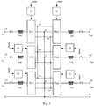
- Fig.1 shows a single phase 2 wire UPS circuit with a single phase line L and a single neutral line N, from which the AC/DC/AC conversion process of this UPS circuit is clear.
- the single phase 2 wire UPS circuit comprises a rectification phase leg PL1 for rectification and an inversion phase leg PL2 for inversion.
- Gate drivers G control the rectification phase leg PL1 and inversion phase leg PL2 corresponding thereto in response to a PWM signal.
- the AC mains power supply is transmitted from an input end T in to the load of the UPS through a rectification inductor L rec , the rectification phase leg PL1, the inversion phase leg PL2, an inversion inductor L inv and an output end Tout.
- Fig. 2 shows a 3 phase 3 wire UPS circuit with three phase lines L1, L2 and L3, which comprises three rectification phase legs PL1 and three inversion phase legs PL2 controlled by the corresponding gate drivers respectively.
- Fig. 3 shows a 3 phase 4 wire UPS circuit with three phase lines L1, L2, L3 and one neutral line N, the structure of which is similar to that of the 3 phase 3 wire UPS circuit shown in Fig. 2 , except for having a further neutral line N.
- the inversion phase legs are generally configured into a multi-level conversion topology which requires many semiconductor devices.
- an object of the present invention is to provide a UPS circuit which may avoid the drawbacks of the prior art.
- a UPS circuit comprising:
- the structure of the redundant inversion phase leg is identical to that of the inversion phase leg.
- the failure detection device comprises a plurality of failure detection modules, each of which is used for detecting a corresponding inversion phase leg.
- control device comprises a switching device, which is used for connecting the redundant inversion phase leg to an output end of a phase line corresponding to the failed inversion phase leg, so as to replace the failed inversion phase leg.
- the switching device comprises one or more switches, when a failure occurs, one of the switches is closed to connect the redundant inversion phase leg to the output end of the phase line corresponding to the failed inversion phase leg, so as to replace the failed inversion phase leg.
- the UPS circuit is a single phase 2 wire system, a 3 phase 3 wire system or a 3 phase 4 wire system.
- the single phase 2 wire UPS circuit or 3 phase 4 wire UPS circuit comprises a neutral line
- the redundant inversion phase leg is connected to the neutral line for injecting a zero sequence component into the neutral point when no failure occurs in the inversion phase leg.
- the redundant inversion phase leg is configured to disconnect from the neutral line if the inversion phase leg fails.
- the redundant inversion phase leg acts as a balancer to balance the voltage of a DC bus.
- the UPS circuit with the redundant inversion phase leg provided by the present invention can significantly improve the reliability.
- the reliability of the whole UPS can be ensured even when a multi-level inversion phase leg with more semiconductor devices and a higher failure rate is adopted. Therefore, the efficiency can be improved on the premise of a high reliability.
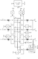
- the embodiment provides a 3 phase 3 wire UPS circuit with three phase lines L1, L2 and L3, the structure of which is shown in Fig. 4 .
- the UPS circuit comprises three rectification phase legs PL1 for rectification and three inversion phase legs PL21, PL22 and PL23 for inversion.
- Each gate driver G controls a corresponding phase leg in response to a PWM signal from a logic control module.
- the AC mains power supply is transmitted from input ends T in of the three phase lines L1, L2 and L3 to the loads of the UPS through rectification inductors L rec , the rectification phase legs PL1, the inversion phase legs PL21, PL22 and PL23, inversion inductors L inv , and output ends T out .
- each inversion phase leg has a corresponding failure detection module D.
- the failure detection modules D are used to detect whether a failure happens in the corresponding phase legs.
- the failure detection modules D send failure signals FD to the logic control module when a failure is detected.
- the UPS circuit of the present embodiment further comprises an additional redundant inversion phase leg PL2a, the structure and input connection way of which are the same as those of the inversion phase legs PL21, PL22 and PL23.
- An output end of the redundant inversion phase leg PL2a is connected to output ends T out of the three phase lines L1, L2 and L3 via an additional redundant inversion inductor L N and three switches 1, 2 and 3 within a switching device SW.
- the redundant inversion phase leg PL2a also has a corresponding gate driver G controlled by the PWM signal from the logic control module.
- the failure detection module D corresponding to the failed inversion phase leg sends a failure signal FD to the logic control module upon detecting the failure.
- the logic control module determines which inversion phase leg fails according to the failure signal FD, stops controlling the gate driver G corresponding to the failed inversion phase leg according to the determination, sends a control signal SW_CTRL to the switching device SW in order to turn on the switch within the switching device SW corresponding to the failed inversion phase leg, and thus replaces the failed inversion phase leg with the redundant inversion phase leg PL2a, so as to ensure the normal operation of the UPS.
- the failure detection module D corresponding to the inversion phase leg PL22 sends a failure signal FD to the logic control module.
- the logic control module determines that the inversion phase leg PL22 fails according to the failure signal FD, sends a control signal SW_CTRL to the switching device SW to turn on the switch 2 within the switching device SW, and thus makes the output end of the redundant inversion phase leg PL2a connect to the output end of the phase line L2 to replace the failed inversion phase leg PL22.
- the logic control module makes the switch 1 within the switching device SW turn on, so as to make the output end of the redundant inversion phase leg PL2a connect to the output end of the phase line L1 to replace the failed inversion phase leg PL21. If the inversion phase leg PL23 fails, the logic control module makes the switch 3 within the switching device SW turn on, so as to make the output end of the redundant inversion phase leg PL2a connect to the output end of the phase line L3 to replace the failed inversion phase leg PL23.
- the UPS circuit with the redundant inversion phase leg provided by the present embodiment can significantly improve the reliability of the UPS.
- the reliability of the whole UPS can be ensured even when a multi-level inversion phase leg with more semiconductor devices and a higher failure rate is adopted. Therefore, the efficiency can be improved on the premise of a high reliability.
- the redundant inversion phase leg of the present invention also can be applied to other types of UPS circuits with inversion phase legs, such as a 3 phase 4 wire UPS circuit.
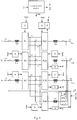
- Fig. 5 shows the 3 phase 4 wire UPS circuit with a redundant inversion phase leg PL2a of the present invention, wherein an output end of the redundant inversion phase leg is connected to a neutral line via a redundant inductor and a closed switch 0 within a switching device SW.
- the redundant inversion phase leg acts for modulation when no failure occurs in inversion phase legs.
- the 3 phase 4 wire circuit may have unbalanced loads.
- the L1 phase current can return to a DC bus via a loop consisting of L N and IGBT in the redundant inversion phase leg.
- the switch 0 within the switching device is switched to the other side to make the redundant inversion phase leg disconnect from the neutral line N and make the midpoint M of the DC bus voltage connect to the neutral line N.
- the phase voltage can use the bus voltage midpoint M as a reference to ensure that an AC is output, i.e., the transient voltage may be positive or negative.
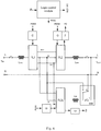
- the redundant inversion phase leg can further be applied to the single phase 2 wire UPS circuit. Similar to the 3 phase 4 wire UPS circuit, the output end of the redundant inversion phase leg PL2a is connected to the neutral line via the redundant inversion inductor L N and the closed switch 0 within the switching device SW.
- the redundant inversion phase leg acts for modulation if no failure occurs in the inversion phase leg PL2.
- the switch 1 is closed by controlling the switching device SW so as to replace the failed inversion phase leg with the redundant inversion phase leg.
- the switch 0 within the switching device is switched to the other side to make the redundant inversion device disconnect from the neutral line N and make the midpoint M of the DC bus voltage connect to the neutral line N.
- the redundant inversion phase leg is idle and acts for modulation.
- a zero sequence component is injected into the neutral point to lower the DC bus voltage and the switching times of the semiconductor devices during each mains power supply cycle, so as to further improve the efficiency of the system.
- the zero sequence component is injected into the neutral point to lower the DC bus voltage and the switching times of the semiconductor devices during each mains power supply cycle, so as to further improve the efficiency of a 3 phase 4 line system.
- the redundant inversion phase leg may be idle (see Fig. 4 ), or act as a balancer to balance the DC bus voltage when the UPS desires.
- the switch 0 When acting as a balancer, the switch 0 is closed when no failure occurs in the inversion phase legs. If the voltage between DC+ and M is higher than that between DC- and M, the balance between the positive and negative voltages of the DC bus may be realized by storing the excess energy of DC+ in the inductor L N and feeding the energy back to the DC- by controlling the phase leg PWM, and vice versa.
- the switch 0 is opened, and one of the switches 1, 2 and 3 corresponding to the failed inversion phase leg is closed, so as to replace the failed inversion phase leg with the redundant inversion phase leg.
- the switching device SW is not limited to that described above.
- the present invention can be realized with any switching device being able to selectively connect the redundant inversion phase leg to the output end of one phase line.
- the switching device SW is preferably a semiconductor device.
- the redundant inversion phase leg may transiently replace the failed inversion phase leg to achieve continuous AC power from the output end Tout.
- it will take a little time to close contacts of a mechanical switching device SW therefore it is impossible to transiently replace the failed inversion phase leg with the redundant inversion phase leg.
- the AC power does not output from the output end T out for an instant.
- the UPS is configured to work in a bypass mode (i.e., the rectification phase legs and the inversion phase legs are all bypassed. Now, the output end Tout of the UPS is directly powered by the mains power supply.), then the failed inversion phase leg is powered off. Meanwhile, the redundant inversion phase leg is connected to the circuit to replace the failed inversion phase leg by controlling the switching device SW. After completing the replacement, the UPS is switched back to an online mode from the bypass mode, so as to replace the failed inversion phase leg with the redundant inversion phase leg.
- a corresponding failure detection module D is provided for each inversion phase leg. But this is only for illustration. According to other embodiments of the present invention, other ways can be used to detect which inversion phase leg fails. For example, all the inversion phase legs may be detected by a centralized failure detection device. A person skilled in the art may choose different failure location methods based on actual demands.
- each adopted inversion phase leg may consist of discrete semiconductor devices or modules.
- the inversion phase legs may be configured into double-level conversion topology or multi-level conversion topology to improve the efficiency of the UPS system.
- Figs. 7a-7c show three topologies of inversion phase legs, the structures of which are shown in the dashed boxes of Figs. 7a-7c .
- Fig. 7a shows an inversion phase leg with a T shaped three-level conversion topology.
- Fig. 7b shows an inversion phase leg with a double-level conversion topology.
- Fig. 7c shows an inversion phase leg with a deformed I shaped three-level conversion topology.
- the above topologies of inversion phase legs are only exemplary. A person skilled in the art may choose various types of topological inversion phase legs based on actual demands.
Landscapes
- Engineering & Computer Science (AREA)
- Power Engineering (AREA)
- Business, Economics & Management (AREA)
- Emergency Management (AREA)
- Inverter Devices (AREA)
- Supply And Distribution Of Alternating Current (AREA)
Abstract
Description
- The present invention relates to a UPS circuit and, more particularly, to a UPS circuit comprising phase legs.
- A UPS (Uninterruptible Power Supply) is an alternating current power supply with an energy storage device, which provides uninterruptible power to a load using the energy storage device such as a battery during power failures. When the mains power supply is available, the UPS regulates the mains power supply and supplies it to the load. When the mains power supply is not available (power failure), the UPS supplies alternating currents (AC) to the load using the energy storage device, so as to keep the load working normally and protect the software and hardware of the load from damage.
- In order to filter the power input, the UPS commonly adopts a structure for AC/DC/AC conversion to provide a pure electric power to the load. Wherein, the AC/DC link converts the AC mains power supply into a smooth DC bus voltage and then provides energy to the next DC/AC link. A conventional AC/DC is realized by uncontrolled rectifier diodes or half controlled SCR and has a low input power factor and a high current harmonics, which will pollute the power grid. A modem AC/DC adopts active semiconductor devices, which can smooth the DC bus voltage and correct the power factor, and thus reduce the pollution to the power grid and ensure a green power grid. A DC/AC link is used to convert the DC bus voltage originating from the AC/DC or the electricity energy storage device into a pure sinusoidal output voltage, so as to ensure the power supply quality and uninterrupted electricity for the load.
-
Fig.1 shows asingle phase 2 wire UPS circuit with a single phase line L and a single neutral line N, from which the AC/DC/AC conversion process of this UPS circuit is clear. As shown inFig. 1 , thesingle phase 2 wire UPS circuit comprises a rectification phase leg PL1 for rectification and an inversion phase leg PL2 for inversion. Gate drivers G control the rectification phase leg PL1 and inversion phase leg PL2 corresponding thereto in response to a PWM signal. The AC mains power supply is transmitted from an input end Tin to the load of the UPS through a rectification inductor Lrec, the rectification phase leg PL1, the inversion phase leg PL2, an inversion inductor Linv and an output end Tout. -
Fig. 2 shows a 3phase 3 wire UPS circuit with three phase lines L1, L2 and L3, which comprises three rectification phase legs PL1 and three inversion phase legs PL2 controlled by the corresponding gate drivers respectively.Fig. 3 shows a 3 phase 4 wire UPS circuit with three phase lines L1, L2, L3 and one neutral line N, the structure of which is similar to that of the 3phase 3 wire UPS circuit shown inFig. 2 , except for having a further neutral line N. - Reliability and efficiency are two of the most important performances of the UPS. At present, in order to obtain higher efficiency, the inversion phase legs are generally configured into a multi-level conversion topology which requires many semiconductor devices. However, the more the semiconductor devices are, the poorer the reliability is. And thus the reliability of the inversion phase legs decreases. Since the inversion phase legs are common modules of the mains power supply mode and the battery mode, the decrease of the reliability will severely affect the reliability of the whole UPS.
- In view of the foregoing, an object of the present invention is to provide a UPS circuit which may avoid the drawbacks of the prior art.
- A UPS circuit is provided, comprising:
- a rectification phase leg for rectification, which is used for converting a received alternating current into a direct current;
- an inversion phase leg for inversion, which is used for inverting the direct current output from the rectification phase leg into an alternating current;
- a failure detection device, which is used for detecting whether the inversion phase legs fails;
- a redundant inversion phase leg, an input end of which is connected to an output end of the rectification phase leg;
- a control device, which is used for receiving a signal sent by the failure detection device and also used for replacing a failed inversion phase leg with the redundant inversion phase leg when a failure occurs.
- Preferably, the structure of the redundant inversion phase leg is identical to that of the inversion phase leg.
- Preferably, the failure detection device comprises a plurality of failure detection modules, each of which is used for detecting a corresponding inversion phase leg.
- Preferably, the control device comprises a switching device, which is used for connecting the redundant inversion phase leg to an output end of a phase line corresponding to the failed inversion phase leg, so as to replace the failed inversion phase leg.
- Preferably, the switching device comprises one or more switches, when a failure occurs, one of the switches is closed to connect the redundant inversion phase leg to the output end of the phase line corresponding to the failed inversion phase leg, so as to replace the failed inversion phase leg.
- Preferably, the UPS circuit is a
single phase 2 wire system, a 3phase 3 wire system or a 3 phase 4 wire system. - Preferably, the
single phase 2 wire UPS circuit or 3 phase 4 wire UPS circuit comprises a neutral line, the redundant inversion phase leg is connected to the neutral line for injecting a zero sequence component into the neutral point when no failure occurs in the inversion phase leg. - Preferably, in the
single phase 2 wire UPS circuit or 3 phase 4 wire UPS circuit, the redundant inversion phase leg is configured to disconnect from the neutral line if the inversion phase leg fails. - Preferably, in the 3
phase 2 wire UPS circuit, the redundant inversion phase leg acts as a balancer to balance the voltage of a DC bus. - The UPS circuit with the redundant inversion phase leg provided by the present invention can significantly improve the reliability. The reliability of the whole UPS can be ensured even when a multi-level inversion phase leg with more semiconductor devices and a higher failure rate is adopted. Therefore, the efficiency can be improved on the premise of a high reliability.
- The present invention will be further explained in combination with the embodiments with reference to the accompanying figures, wherein:
-
Fig. 1 is a schematic diagram of a prior artsingle phase 2 wire UPS circuit; -
Fig. 2 is a schematic diagram of aprior art 3phase 3 wire UPS circuit; -
Fig. 3 is a schematic diagram of aprior art 3 phase 4 wire UPS circuit; -
Fig. 4 is a schematic diagram of a 3phase 3 wire UPS circuit according to one embodiment of the present invention; -
Fig. 5 is a schematic diagram of a 3 phase 4 wire UPS circuit according to one embodiment of the present invention; -
Fig. 6 is a schematic diagram of asingle phase 2 wire UPS circuit according to one embodiment of the present invention; and -
Figs. 7a-7c show three topologies of the inverter phase legs. - In the following parts, the present invention will be described in greater details with reference to the embodiments and the accompanying drawings so as to make its objects, solutions and advantages clearer. It should be understood that the specific embodiments described herein only intend to interpret the present invention, without making any limitation thereto.
- The embodiment provides a 3
phase 3 wire UPS circuit with three phase lines L1, L2 and L3, the structure of which is shown inFig. 4 . The UPS circuit comprises three rectification phase legs PL1 for rectification and three inversion phase legs PL21, PL22 and PL23 for inversion. Each gate driver G controls a corresponding phase leg in response to a PWM signal from a logic control module. The AC mains power supply is transmitted from input ends Tin of the three phase lines L1, L2 and L3 to the loads of the UPS through rectification inductors Lrec, the rectification phase legs PL1, the inversion phase legs PL21, PL22 and PL23, inversion inductors Linv, and output ends Tout. In addition, each inversion phase leg has a corresponding failure detection module D. The failure detection modules D are used to detect whether a failure happens in the corresponding phase legs. The failure detection modules D send failure signals FD to the logic control module when a failure is detected. - Moreover, the UPS circuit of the present embodiment further comprises an additional redundant inversion phase leg PL2a, the structure and input connection way of which are the same as those of the inversion phase legs PL21, PL22 and PL23. An output end of the redundant inversion phase leg PL2a is connected to output ends Tout of the three phase lines L1, L2 and L3 via an additional redundant inversion inductor LN and three
switches - If one of the inversion phase legs fails due to the failure of the semiconductor devices thereof, the failure detection module D corresponding to the failed inversion phase leg sends a failure signal FD to the logic control module upon detecting the failure. The logic control module determines which inversion phase leg fails according to the failure signal FD, stops controlling the gate driver G corresponding to the failed inversion phase leg according to the determination, sends a control signal SW_CTRL to the switching device SW in order to turn on the switch within the switching device SW corresponding to the failed inversion phase leg, and thus replaces the failed inversion phase leg with the redundant inversion phase leg PL2a, so as to ensure the normal operation of the UPS.
- For example, if the inversion phase leg PL22 fails, the failure detection module D corresponding to the inversion phase leg PL22 sends a failure signal FD to the logic control module. The logic control module determines that the inversion phase leg PL22 fails according to the failure signal FD, sends a control signal SW_CTRL to the switching device SW to turn on the
switch 2 within the switching device SW, and thus makes the output end of the redundant inversion phase leg PL2a connect to the output end of the phase line L2 to replace the failed inversion phase leg PL22. - As shown in
Fig. 4 , if the inversion phase leg PL21 fails, the logic control module makes the switch 1 within the switching device SW turn on, so as to make the output end of the redundant inversion phase leg PL2a connect to the output end of the phase line L1 to replace the failed inversion phase leg PL21. If the inversion phase leg PL23 fails, the logic control module makes theswitch 3 within the switching device SW turn on, so as to make the output end of the redundant inversion phase leg PL2a connect to the output end of the phase line L3 to replace the failed inversion phase leg PL23. - In view of above, the UPS circuit with the redundant inversion phase leg provided by the present embodiment can significantly improve the reliability of the UPS. The reliability of the whole UPS can be ensured even when a multi-level inversion phase leg with more semiconductor devices and a higher failure rate is adopted. Therefore, the efficiency can be improved on the premise of a high reliability.
- According to other embodiments of the present invention, the redundant inversion phase leg of the present invention also can be applied to other types of UPS circuits with inversion phase legs, such as a 3 phase 4 wire UPS circuit.
Fig. 5 shows the 3 phase 4 wire UPS circuit with a redundant inversion phase leg PL2a of the present invention, wherein an output end of the redundant inversion phase leg is connected to a neutral line via a redundant inductor and aclosed switch 0 within a switching device SW. The redundant inversion phase leg acts for modulation when no failure occurs in inversion phase legs. The 3 phase 4 wire circuit may have unbalanced loads. For example, if just the L1 phase has a load, the L1 phase current can return to a DC bus via a loop consisting of LN and IGBT in the redundant inversion phase leg. When one of the inversion phase legs fails, by controlling the switching device SW, the failed inversion phase leg is replaced by the redundant inversion phase leg, theswitch 0 within the switching device is switched to the other side to make the redundant inversion phase leg disconnect from the neutral line N and make the midpoint M of the DC bus voltage connect to the neutral line N. After the midpoint M of the DC bus voltage is connected to the neutral line N, a loop of the phase current returning to the bus is formed, so as to carry a single phase or three phase unbalanced load. In addition, the phase voltage can use the bus voltage midpoint M as a reference to ensure that an AC is output, i.e., the transient voltage may be positive or negative. - For another example, as shown in
Fig. 6 , the redundant inversion phase leg can further be applied to thesingle phase 2 wire UPS circuit. Similar to the 3 phase 4 wire UPS circuit, the output end of the redundant inversion phase leg PL2a is connected to the neutral line via the redundant inversion inductor LN and theclosed switch 0 within the switching device SW. The redundant inversion phase leg acts for modulation if no failure occurs in the inversion phase leg PL2. When the inversion phase leg PL2 fails, the switch 1 is closed by controlling the switching device SW so as to replace the failed inversion phase leg with the redundant inversion phase leg. At the same time, theswitch 0 within the switching device is switched to the other side to make the redundant inversion device disconnect from the neutral line N and make the midpoint M of the DC bus voltage connect to the neutral line N. - In the
single phase 2 wire or 3 phase 4 wire UPS circuit with a neutral line described above, if no failure occurs in the inversion phase legs, the redundant inversion phase leg is idle and acts for modulation. A zero sequence component is injected into the neutral point to lower the DC bus voltage and the switching times of the semiconductor devices during each mains power supply cycle, so as to further improve the efficiency of the system. For example, by injecting a specific harmonic or a specific choice of SVPWM zero vectors with SPWM, the zero sequence component is injected into the neutral point to lower the DC bus voltage and the switching times of the semiconductor devices during each mains power supply cycle, so as to further improve the efficiency of a 3 phase 4 line system. For injecting a specific harmonic or a specific choice of SVPWM zero vectors with SPWM, reference is made to B.Kaku, et.al, "Switching loss minimized space vector PWM method for IGBT three- level inverter", IEE Proc.Electr. Power Appl., vol. 144, no.3, pp.182-190, May 1997. - For a 3
phase 3 wire system, the redundant inversion phase leg may be idle (seeFig. 4 ), or act as a balancer to balance the DC bus voltage when the UPS desires. When acting as a balancer, theswitch 0 is closed when no failure occurs in the inversion phase legs. If the voltage between DC+ and M is higher than that between DC- and M, the balance between the positive and negative voltages of the DC bus may be realized by storing the excess energy of DC+ in the inductor LN and feeding the energy back to the DC- by controlling the phase leg PWM, and vice versa. When a failure occurs, theswitch 0 is opened, and one of theswitches - According to other embodiments of the present invention, the switching device SW is not limited to that described above. The present invention can be realized with any switching device being able to selectively connect the redundant inversion phase leg to the output end of one phase line. In addition, the switching device SW is preferably a semiconductor device. In this case, the redundant inversion phase leg may transiently replace the failed inversion phase leg to achieve continuous AC power from the output end Tout. However, it will take a little time to close contacts of a mechanical switching device SW, therefore it is impossible to transiently replace the failed inversion phase leg with the redundant inversion phase leg. During the replacing, the AC power does not output from the output end Tout for an instant. Therefore, in case of adopting the mechanical switching device SW, if one of the inversion phase legs fails, firstly the UPS is configured to work in a bypass mode (i.e., the rectification phase legs and the inversion phase legs are all bypassed. Now, the output end Tout of the UPS is directly powered by the mains power supply.), then the failed inversion phase leg is powered off. Meanwhile, the redundant inversion phase leg is connected to the circuit to replace the failed inversion phase leg by controlling the switching device SW. After completing the replacement, the UPS is switched back to an online mode from the bypass mode, so as to replace the failed inversion phase leg with the redundant inversion phase leg.
- In the UPS circuit provided in above embodiments, a corresponding failure detection module D is provided for each inversion phase leg. But this is only for illustration. According to other embodiments of the present invention, other ways can be used to detect which inversion phase leg fails. For example, all the inversion phase legs may be detected by a centralized failure detection device. A person skilled in the art may choose different failure location methods based on actual demands.
- In the UPS circuit of the present invention, each adopted inversion phase leg may consist of discrete semiconductor devices or modules. The inversion phase legs may be configured into double-level conversion topology or multi-level conversion topology to improve the efficiency of the UPS system. For example,
Figs. 7a-7c show three topologies of inversion phase legs, the structures of which are shown in the dashed boxes ofFigs. 7a-7c . Wherein,Fig. 7a shows an inversion phase leg with a T shaped three-level conversion topology.Fig. 7b shows an inversion phase leg with a double-level conversion topology. AndFig. 7c shows an inversion phase leg with a deformed I shaped three-level conversion topology. The above topologies of inversion phase legs are only exemplary. A person skilled in the art may choose various types of topological inversion phase legs based on actual demands. - It should be appreciated that the above embodiments are only used to interpret, not to limit, the solutions of the invention. Embodiments of the present invention have been described in terms of the preferred embodiments, but the present invention is not limited to the embodiments described above, and various amendments and changes may be made within the scope of the present invention.
Claims (10)
- A UPS circuit, comprising:a rectification phase leg for rectification, which is used for converting a received alternating current into a direct current;an inversion phase leg for inversion, which is used for inverting the direct current output from the rectification phase leg into an alternating current;a failure detection device, which is used for detecting whether the inversion phase leg fails;a redundant inversion phase leg, an input end of which is connected to an output end of the rectification phase leg;a control device, which is used for receiving a signal sent by the failure detection device and also used for replacing a failed inversion phase leg with the redundant inversion phase leg when a failure occurs.
- The UPS circuit according to claim 1, wherein the structure of the redundant inversion phase leg is identical to that of the inversion phase leg.
- The UPS circuit according to claim 1, wherein the failure detection device comprises a plurality of failure detection modules, each of which is used for detecting a corresponding inversion phase leg.
- The UPS circuit according to claim 1, wherein the control device comprises a switching device, which is used for connecting the redundant inversion phase leg to an output end of a phase line corresponding to the failed inversion phase leg, so as to replace the failed inversion phase leg.
- The UPS circuit according to claim 4, wherein the switching device comprises one or more switches, and when a failure occurs, one of the switches is closed to connect the redundant inversion phase leg to the output end of the phase line corresponding to the failed inversion phase leg, so as to replace the failed inversion phase leg.
- The UPS circuit according to claim 1, wherein the UPS circuit is a 3 phase 3 wire system.
- The UPS circuit according to claim 1, wherein the UPS circuit is a single phase 2 wire system or a 3 phase 4 wire system.
- The UPS circuit according to claim 7, wherein the UPS circuit comprises a neutral line, and the redundant inversion phase leg is connected to the neutral line for injecting a zero sequence component into the neutral point when no failure occurs in the inversion phase leg.
- The UPS circuit according to claim 8, wherein the redundant inversion phase leg is configured to disconnect from the neutral line if the inversion phase leg fails.
- The UPS circuit according to claim 6, wherein the redundant inversion phase leg acts as a balancer to balance the voltage of a DC bus.
Applications Claiming Priority (2)
| Application Number | Priority Date | Filing Date | Title |
|---|---|---|---|
| CN201410076489.0A CN104901410A (en) | 2014-03-04 | 2014-03-04 | UPS circuit |
| PCT/CN2015/073393 WO2015131781A1 (en) | 2014-03-04 | 2015-02-28 | Ups circuit |
Publications (3)
| Publication Number | Publication Date |
|---|---|
| EP3116096A1 true EP3116096A1 (en) | 2017-01-11 |
| EP3116096A4 EP3116096A4 (en) | 2017-11-22 |
| EP3116096B1 EP3116096B1 (en) | 2021-08-25 |
Family
ID=54033891
Family Applications (1)
| Application Number | Title | Priority Date | Filing Date |
|---|---|---|---|
| EP15758204.0A Active EP3116096B1 (en) | 2014-03-04 | 2015-02-28 | Ups circuit |
Country Status (4)
| Country | Link |
|---|---|
| US (1) | US10536030B2 (en) |
| EP (1) | EP3116096B1 (en) |
| CN (1) | CN104901410A (en) |
| WO (1) | WO2015131781A1 (en) |
Cited By (2)
| Publication number | Priority date | Publication date | Assignee | Title |
|---|---|---|---|---|
| EP3309927A1 (en) * | 2016-10-13 | 2018-04-18 | Schneider Electric IT Corporation | Dc-link bus balancer |
| WO2019007690A1 (en) * | 2017-07-04 | 2019-01-10 | Siemens Aktiengesellschaft | UNINTERRUPTIBLE POWER SUPPLY |
Families Citing this family (11)
| Publication number | Priority date | Publication date | Assignee | Title |
|---|---|---|---|---|
| CN110071521B (en) * | 2018-01-23 | 2021-09-03 | 台达电子企业管理(上海)有限公司 | Power distribution equipment and power distribution method |
| CN108736477A (en) * | 2018-07-16 | 2018-11-02 | 张哲� | With power utilization network topology |
| US11381159B2 (en) | 2018-09-06 | 2022-07-05 | Cornell University | High power density power converter and uninterruptible power supply circuit and methods |
| CN109888912B (en) * | 2019-03-18 | 2020-07-10 | 中国石油大学(华东) | Standby power supply based on unbalanced AC/DC single/two-phase fault and its application |
| US11349336B2 (en) * | 2020-03-03 | 2022-05-31 | Delta Electronics, Inc. | Method for operating power factor correction circuit and method for operating uninterruptible power supply apparatus |
| CN112187084B (en) * | 2020-09-27 | 2022-07-05 | 新风光电子科技股份有限公司 | Frequency conversion integrated machine main loop topological structure with redundancy design |
| CN112671253B (en) * | 2021-03-15 | 2021-06-22 | 四川华泰电气股份有限公司 | Cascaded H-bridge converter, open-circuit fault redundancy processing method, medium, and apparatus |
| DE102022127077A1 (en) * | 2022-10-17 | 2024-04-18 | Schaeffler Technologies AG & Co. KG | Converter unit for supplying two electrical loads of a vehicle and method for its operation and vehicle |
| CN115663989B (en) * | 2022-10-20 | 2023-04-28 | 上海山源电子科技股份有限公司 | Commercial power inversion switching control method and circuit |
| CN117526544B (en) * | 2024-01-03 | 2024-05-17 | 深圳市英威腾电源有限公司 | Control method and system of UPS module, electronic equipment and storage medium |
| CN119210125B (en) * | 2024-11-29 | 2025-03-28 | 厦门均好科技有限公司 | A power adapter switch power control system |
Family Cites Families (33)
| Publication number | Priority date | Publication date | Assignee | Title |
|---|---|---|---|---|
| US5343079A (en) | 1991-02-25 | 1994-08-30 | Regents Of The University Of Minnesota | Standby power supply with load-current harmonics neutralizer |
| JPH08116675A (en) | 1994-10-18 | 1996-05-07 | Meidensha Corp | Power converter |
| JP3647554B2 (en) * | 1996-07-12 | 2005-05-11 | 株式会社東芝 | X-ray high voltage device |
| US6058031A (en) * | 1997-10-23 | 2000-05-02 | General Electric Company | Five level high power motor drive converter and control system |
| US6275958B1 (en) * | 1998-10-28 | 2001-08-14 | International Business Machines Corporation | Fault detection in a redundant power converter |
| US6288916B1 (en) * | 1999-10-15 | 2001-09-11 | Alpha Technologies, Inc. | Multiple output uninterruptible alternating current power supplies for communications system |
| CN100334801C (en) | 2000-12-07 | 2007-08-29 | 株式会社安川电机 | Neutral Point Clamped Pulse Width Modulation Inverter Device |
| JP2003259654A (en) | 2002-03-05 | 2003-09-12 | Toshiba Corp | Power converter |
| US6831442B2 (en) * | 2002-07-03 | 2004-12-14 | General Motors Corporation | Utilizing zero-sequence switchings for reversible converters |
| US7088601B2 (en) * | 2004-01-23 | 2006-08-08 | Eaton Power Quality Corporation | Power conversion apparatus and methods using DC bus shifting |
| JP4431519B2 (en) * | 2005-04-11 | 2010-03-17 | 日立Geニュークリア・エナジー株式会社 | Reactor coolant recirculation pump power supply |
| EP1713155B1 (en) * | 2005-04-12 | 2012-10-17 | DET International Holding Limited | Power supply arrangement |
| FR2892243B1 (en) * | 2005-10-13 | 2008-01-18 | Airbus France Sas | RECONFIGURABLE VOLTAGE INVERTER WITH TROUBLESHOOTING |
| CN2859902Y (en) * | 2005-11-28 | 2007-01-17 | 王三功 | In-line duplicate supply control device and in-line duplicate supply electric power unit |
| JP2007336750A (en) | 2006-06-16 | 2007-12-27 | Toshiba Corp | Auxiliary power supply for railway vehicles |
| US7492060B2 (en) * | 2006-09-01 | 2009-02-17 | Atomic Energy Council - Institute Of Nuclear Energy Research | Fault-tolerant circuit device in fuel cell AC inverter |
| US7800924B2 (en) * | 2007-03-27 | 2010-09-21 | Eaton Corporation | Power converter apparatus and methods using neutral coupling circuits with interleaved operation |
| JP5474772B2 (en) * | 2007-06-01 | 2014-04-16 | ディーアールエス パワー アンド コントロール テクノロジーズ インコーポレーテッド | Three-level neutral point fixed conversion device and control method thereof |
| US20100172166A1 (en) * | 2009-01-07 | 2010-07-08 | Tejinder Singh | Plug-in neutral regulator for 3-phase 4-wire inverter/converter system |
| JP5436537B2 (en) * | 2009-03-18 | 2014-03-05 | 東芝三菱電機産業システム株式会社 | Uninterruptible power system |
| MX2011013519A (en) * | 2009-06-18 | 2012-02-22 | Abb Technology Ag | An arrangement for exchanging power. |
| CN101582671B (en) | 2009-06-23 | 2011-07-27 | 南京航空航天大学 | Power converter for switch reluctance starter/generator |
| JP5460270B2 (en) * | 2009-11-30 | 2014-04-02 | 株式会社東芝 | X-ray diagnostic equipment |
| FR2954618B1 (en) * | 2009-12-22 | 2012-12-28 | Astrium Sas | RECONFIGURABLE, TROUBLESHOOTING INVERTER FOR POWERING A PERMANENT MAGNET SYNCHRONOUS THREE-PHASE MOTOR, AND ALL OF SAID INVERTER AND MOTOR |
| JP2011193589A (en) | 2010-03-12 | 2011-09-29 | Fuji Electric Co Ltd | Power converter |
| US20110278932A1 (en) * | 2010-05-13 | 2011-11-17 | Eaton Corporation | Uninterruptible power supply systems and methods using isolated interface for variably available power source |
| US8471514B2 (en) * | 2010-09-30 | 2013-06-25 | Rockwell Automation Technologies, Inc. | Adaptive harmonic reduction apparatus and methods |
| US8837096B2 (en) * | 2012-03-13 | 2014-09-16 | Thoratec Corporation | Fault monitor for fault tolerant implantable pump |
| JP5344063B2 (en) * | 2012-04-02 | 2013-11-20 | 富士電機株式会社 | Power converter |
| US9214874B2 (en) * | 2012-07-31 | 2015-12-15 | Yashomani Y. Kolhatkar | Intelligent level transition systems and methods for transformerless uninterruptible power supply |
| JP5606506B2 (en) * | 2012-09-20 | 2014-10-15 | 三菱電機株式会社 | Drive control device and drive control method |
| CN103219749A (en) | 2012-11-28 | 2013-07-24 | 东方日立(成都)电控设备有限公司 | Grid-connected photovoltaic power generation system capable of dynamically switching invert units and switching method thereof |
| CN103368231B (en) * | 2013-07-05 | 2015-03-11 | 华为技术有限公司 | Uninterruptible power supply circuit |
-
2014
- 2014-03-04 CN CN201410076489.0A patent/CN104901410A/en active Pending
-
2015
- 2015-02-28 EP EP15758204.0A patent/EP3116096B1/en active Active
- 2015-02-28 WO PCT/CN2015/073393 patent/WO2015131781A1/en not_active Ceased
- 2015-02-28 US US15/123,131 patent/US10536030B2/en active Active
Cited By (2)
| Publication number | Priority date | Publication date | Assignee | Title |
|---|---|---|---|---|
| EP3309927A1 (en) * | 2016-10-13 | 2018-04-18 | Schneider Electric IT Corporation | Dc-link bus balancer |
| WO2019007690A1 (en) * | 2017-07-04 | 2019-01-10 | Siemens Aktiengesellschaft | UNINTERRUPTIBLE POWER SUPPLY |
Also Published As
| Publication number | Publication date |
|---|---|
| CN104901410A (en) | 2015-09-09 |
| WO2015131781A1 (en) | 2015-09-11 |
| EP3116096A4 (en) | 2017-11-22 |
| EP3116096B1 (en) | 2021-08-25 |
| US20170077749A1 (en) | 2017-03-16 |
| US10536030B2 (en) | 2020-01-14 |
Similar Documents
| Publication | Publication Date | Title |
|---|---|---|
| US10536030B2 (en) | UPS circuit | |
| US10284006B2 (en) | Uninterruptible power supply system | |
| KR101837742B1 (en) | Grid-connected inverter system with seamless transfer function | |
| US9203323B2 (en) | Very high efficiency uninterruptible power supply | |
| US11342786B2 (en) | 3-wire multiphase UPS with bypass | |
| US9444286B2 (en) | Uninterruptible power supply system | |
| CN102630369A (en) | Power conversion device | |
| KR20130095257A (en) | Hvdc converter comprising fullbridge cells for handling a dc side short circuit | |
| CN112803462A (en) | Forced turn-off method of static transfer switch based on energy storage converter | |
| WO2017024641A1 (en) | Three-phase rectifier boost circuit and control method therefor, and uninterruptible power supply | |
| JP5887501B2 (en) | Grid interconnection device | |
| CN106170916A (en) | There is the uninterrupted power source of balance buck/boost changer | |
| CN117013680A (en) | An uninterruptible power supply and power supply system | |
| CN108551173B (en) | Series-parallel compensator and control method and device thereof | |
| CN111512532B (en) | Device, method for operating such a device and application of such a device | |
| Wei et al. | Control architecture for paralleled current-source-inverter (CSI) based uninterruptible power systems (UPS) | |
| Machado et al. | Fault-tolerant Utility Interface power converter for low-voltage microgrids | |
| CN102420456A (en) | Power supply system for photovoltaic grid-connected inverter | |
| JP7831055B2 (en) | Power converter | |
| JP2017093210A (en) | Uninterruptible power supply | |
| CN211930326U (en) | UPS system of fault-tolerant inverter | |
| CN104283233B (en) | A kind of flexible direct current power transmission system | |
| JP2015095926A (en) | Power conversion system and first charging method therefor | |
| CN211930327U (en) | UPS system based on three-phase six-switch fault-tolerant inverter | |
| JP7251339B2 (en) | power converter |
Legal Events
| Date | Code | Title | Description |
|---|---|---|---|
| PUAI | Public reference made under article 153(3) epc to a published international application that has entered the european phase |
Free format text: ORIGINAL CODE: 0009012 |
|
| STAA | Information on the status of an ep patent application or granted ep patent |
Free format text: STATUS: REQUEST FOR EXAMINATION WAS MADE |
|
| 17P | Request for examination filed |
Effective date: 20160831 |
|
| AK | Designated contracting states |
Kind code of ref document: A1 Designated state(s): AL AT BE BG CH CY CZ DE DK EE ES FI FR GB GR HR HU IE IS IT LI LT LU LV MC MK MT NL NO PL PT RO RS SE SI SK SM TR |
|
| AX | Request for extension of the european patent |
Extension state: BA ME |
|
| DAX | Request for extension of the european patent (deleted) | ||
| A4 | Supplementary search report drawn up and despatched |
Effective date: 20171025 |
|
| RIC1 | Information provided on ipc code assigned before grant |
Ipc: H02J 9/06 20060101ALI20171019BHEP Ipc: H02M 1/32 20070101ALI20171019BHEP Ipc: H02J 9/00 20060101AFI20171019BHEP |
|
| STAA | Information on the status of an ep patent application or granted ep patent |
Free format text: STATUS: EXAMINATION IS IN PROGRESS |
|
| 17Q | First examination report despatched |
Effective date: 20190710 |
|
| RAP1 | Party data changed (applicant data changed or rights of an application transferred) |
Owner name: EATON INTELLIGENT POWER LIMITED |
|
| GRAP | Despatch of communication of intention to grant a patent |
Free format text: ORIGINAL CODE: EPIDOSNIGR1 |
|
| STAA | Information on the status of an ep patent application or granted ep patent |
Free format text: STATUS: GRANT OF PATENT IS INTENDED |
|
| INTG | Intention to grant announced |
Effective date: 20210330 |
|
| GRAS | Grant fee paid |
Free format text: ORIGINAL CODE: EPIDOSNIGR3 |
|
| GRAA | (expected) grant |
Free format text: ORIGINAL CODE: 0009210 |
|
| STAA | Information on the status of an ep patent application or granted ep patent |
Free format text: STATUS: THE PATENT HAS BEEN GRANTED |
|
| AK | Designated contracting states |
Kind code of ref document: B1 Designated state(s): AL AT BE BG CH CY CZ DE DK EE ES FI FR GB GR HR HU IE IS IT LI LT LU LV MC MK MT NL NO PL PT RO RS SE SI SK SM TR |
|
| REG | Reference to a national code |
Ref country code: CH Ref legal event code: EP |
|
| REG | Reference to a national code |
Ref country code: DE Ref legal event code: R096 Ref document number: 602015072619 Country of ref document: DE |
|
| REG | Reference to a national code |
Ref country code: IE Ref legal event code: FG4D Ref country code: AT Ref legal event code: REF Ref document number: 1424792 Country of ref document: AT Kind code of ref document: T Effective date: 20210915 |
|
| REG | Reference to a national code |
Ref country code: LT Ref legal event code: MG9D |
|
| REG | Reference to a national code |
Ref country code: NL Ref legal event code: MP Effective date: 20210825 |
|
| REG | Reference to a national code |
Ref country code: AT Ref legal event code: MK05 Ref document number: 1424792 Country of ref document: AT Kind code of ref document: T Effective date: 20210825 |
|
| PG25 | Lapsed in a contracting state [announced via postgrant information from national office to epo] |
Ref country code: ES Free format text: LAPSE BECAUSE OF FAILURE TO SUBMIT A TRANSLATION OF THE DESCRIPTION OR TO PAY THE FEE WITHIN THE PRESCRIBED TIME-LIMIT Effective date: 20210825 Ref country code: FI Free format text: LAPSE BECAUSE OF FAILURE TO SUBMIT A TRANSLATION OF THE DESCRIPTION OR TO PAY THE FEE WITHIN THE PRESCRIBED TIME-LIMIT Effective date: 20210825 Ref country code: NO Free format text: LAPSE BECAUSE OF FAILURE TO SUBMIT A TRANSLATION OF THE DESCRIPTION OR TO PAY THE FEE WITHIN THE PRESCRIBED TIME-LIMIT Effective date: 20211125 Ref country code: PT Free format text: LAPSE BECAUSE OF FAILURE TO SUBMIT A TRANSLATION OF THE DESCRIPTION OR TO PAY THE FEE WITHIN THE PRESCRIBED TIME-LIMIT Effective date: 20211227 Ref country code: BG Free format text: LAPSE BECAUSE OF FAILURE TO SUBMIT A TRANSLATION OF THE DESCRIPTION OR TO PAY THE FEE WITHIN THE PRESCRIBED TIME-LIMIT Effective date: 20211125 Ref country code: AT Free format text: LAPSE BECAUSE OF FAILURE TO SUBMIT A TRANSLATION OF THE DESCRIPTION OR TO PAY THE FEE WITHIN THE PRESCRIBED TIME-LIMIT Effective date: 20210825 Ref country code: LT Free format text: LAPSE BECAUSE OF FAILURE TO SUBMIT A TRANSLATION OF THE DESCRIPTION OR TO PAY THE FEE WITHIN THE PRESCRIBED TIME-LIMIT Effective date: 20210825 Ref country code: RS Free format text: LAPSE BECAUSE OF FAILURE TO SUBMIT A TRANSLATION OF THE DESCRIPTION OR TO PAY THE FEE WITHIN THE PRESCRIBED TIME-LIMIT Effective date: 20210825 Ref country code: SE Free format text: LAPSE BECAUSE OF FAILURE TO SUBMIT A TRANSLATION OF THE DESCRIPTION OR TO PAY THE FEE WITHIN THE PRESCRIBED TIME-LIMIT Effective date: 20210825 Ref country code: HR Free format text: LAPSE BECAUSE OF FAILURE TO SUBMIT A TRANSLATION OF THE DESCRIPTION OR TO PAY THE FEE WITHIN THE PRESCRIBED TIME-LIMIT Effective date: 20210825 |
|
| PG25 | Lapsed in a contracting state [announced via postgrant information from national office to epo] |
Ref country code: PL Free format text: LAPSE BECAUSE OF FAILURE TO SUBMIT A TRANSLATION OF THE DESCRIPTION OR TO PAY THE FEE WITHIN THE PRESCRIBED TIME-LIMIT Effective date: 20210825 Ref country code: LV Free format text: LAPSE BECAUSE OF FAILURE TO SUBMIT A TRANSLATION OF THE DESCRIPTION OR TO PAY THE FEE WITHIN THE PRESCRIBED TIME-LIMIT Effective date: 20210825 Ref country code: GR Free format text: LAPSE BECAUSE OF FAILURE TO SUBMIT A TRANSLATION OF THE DESCRIPTION OR TO PAY THE FEE WITHIN THE PRESCRIBED TIME-LIMIT Effective date: 20211126 |
|
| PG25 | Lapsed in a contracting state [announced via postgrant information from national office to epo] |
Ref country code: NL Free format text: LAPSE BECAUSE OF FAILURE TO SUBMIT A TRANSLATION OF THE DESCRIPTION OR TO PAY THE FEE WITHIN THE PRESCRIBED TIME-LIMIT Effective date: 20210825 |
|
| PG25 | Lapsed in a contracting state [announced via postgrant information from national office to epo] |
Ref country code: DK Free format text: LAPSE BECAUSE OF FAILURE TO SUBMIT A TRANSLATION OF THE DESCRIPTION OR TO PAY THE FEE WITHIN THE PRESCRIBED TIME-LIMIT Effective date: 20210825 |
|
| REG | Reference to a national code |
Ref country code: DE Ref legal event code: R097 Ref document number: 602015072619 Country of ref document: DE |
|
| PG25 | Lapsed in a contracting state [announced via postgrant information from national office to epo] |
Ref country code: SM Free format text: LAPSE BECAUSE OF FAILURE TO SUBMIT A TRANSLATION OF THE DESCRIPTION OR TO PAY THE FEE WITHIN THE PRESCRIBED TIME-LIMIT Effective date: 20210825 Ref country code: SK Free format text: LAPSE BECAUSE OF FAILURE TO SUBMIT A TRANSLATION OF THE DESCRIPTION OR TO PAY THE FEE WITHIN THE PRESCRIBED TIME-LIMIT Effective date: 20210825 Ref country code: RO Free format text: LAPSE BECAUSE OF FAILURE TO SUBMIT A TRANSLATION OF THE DESCRIPTION OR TO PAY THE FEE WITHIN THE PRESCRIBED TIME-LIMIT Effective date: 20210825 Ref country code: EE Free format text: LAPSE BECAUSE OF FAILURE TO SUBMIT A TRANSLATION OF THE DESCRIPTION OR TO PAY THE FEE WITHIN THE PRESCRIBED TIME-LIMIT Effective date: 20210825 Ref country code: CZ Free format text: LAPSE BECAUSE OF FAILURE TO SUBMIT A TRANSLATION OF THE DESCRIPTION OR TO PAY THE FEE WITHIN THE PRESCRIBED TIME-LIMIT Effective date: 20210825 Ref country code: AL Free format text: LAPSE BECAUSE OF FAILURE TO SUBMIT A TRANSLATION OF THE DESCRIPTION OR TO PAY THE FEE WITHIN THE PRESCRIBED TIME-LIMIT Effective date: 20210825 |
|
| PLBE | No opposition filed within time limit |
Free format text: ORIGINAL CODE: 0009261 |
|
| STAA | Information on the status of an ep patent application or granted ep patent |
Free format text: STATUS: NO OPPOSITION FILED WITHIN TIME LIMIT |
|
| PG25 | Lapsed in a contracting state [announced via postgrant information from national office to epo] |
Ref country code: IT Free format text: LAPSE BECAUSE OF FAILURE TO SUBMIT A TRANSLATION OF THE DESCRIPTION OR TO PAY THE FEE WITHIN THE PRESCRIBED TIME-LIMIT Effective date: 20210825 |
|
| 26N | No opposition filed |
Effective date: 20220527 |
|
| PG25 | Lapsed in a contracting state [announced via postgrant information from national office to epo] |
Ref country code: SI Free format text: LAPSE BECAUSE OF FAILURE TO SUBMIT A TRANSLATION OF THE DESCRIPTION OR TO PAY THE FEE WITHIN THE PRESCRIBED TIME-LIMIT Effective date: 20210825 |
|
| PG25 | Lapsed in a contracting state [announced via postgrant information from national office to epo] |
Ref country code: MC Free format text: LAPSE BECAUSE OF FAILURE TO SUBMIT A TRANSLATION OF THE DESCRIPTION OR TO PAY THE FEE WITHIN THE PRESCRIBED TIME-LIMIT Effective date: 20210825 |
|
| REG | Reference to a national code |
Ref country code: CH Ref legal event code: PL |
|
| REG | Reference to a national code |
Ref country code: BE Ref legal event code: MM Effective date: 20220228 |
|
| PG25 | Lapsed in a contracting state [announced via postgrant information from national office to epo] |
Ref country code: LU Free format text: LAPSE BECAUSE OF NON-PAYMENT OF DUE FEES Effective date: 20220228 |
|
| PG25 | Lapsed in a contracting state [announced via postgrant information from national office to epo] |
Ref country code: LI Free format text: LAPSE BECAUSE OF NON-PAYMENT OF DUE FEES Effective date: 20220228 Ref country code: IE Free format text: LAPSE BECAUSE OF NON-PAYMENT OF DUE FEES Effective date: 20220228 Ref country code: CH Free format text: LAPSE BECAUSE OF NON-PAYMENT OF DUE FEES Effective date: 20220228 |
|
| PG25 | Lapsed in a contracting state [announced via postgrant information from national office to epo] |
Ref country code: BE Free format text: LAPSE BECAUSE OF NON-PAYMENT OF DUE FEES Effective date: 20220228 |
|
| P01 | Opt-out of the competence of the unified patent court (upc) registered |
Effective date: 20230521 |
|
| PG25 | Lapsed in a contracting state [announced via postgrant information from national office to epo] |
Ref country code: HU Free format text: LAPSE BECAUSE OF FAILURE TO SUBMIT A TRANSLATION OF THE DESCRIPTION OR TO PAY THE FEE WITHIN THE PRESCRIBED TIME-LIMIT; INVALID AB INITIO Effective date: 20150228 |
|
| PG25 | Lapsed in a contracting state [announced via postgrant information from national office to epo] |
Ref country code: MK Free format text: LAPSE BECAUSE OF FAILURE TO SUBMIT A TRANSLATION OF THE DESCRIPTION OR TO PAY THE FEE WITHIN THE PRESCRIBED TIME-LIMIT Effective date: 20210825 Ref country code: CY Free format text: LAPSE BECAUSE OF FAILURE TO SUBMIT A TRANSLATION OF THE DESCRIPTION OR TO PAY THE FEE WITHIN THE PRESCRIBED TIME-LIMIT Effective date: 20210825 |
|
| PG25 | Lapsed in a contracting state [announced via postgrant information from national office to epo] |
Ref country code: MT Free format text: LAPSE BECAUSE OF FAILURE TO SUBMIT A TRANSLATION OF THE DESCRIPTION OR TO PAY THE FEE WITHIN THE PRESCRIBED TIME-LIMIT Effective date: 20210825 |
|
| PG25 | Lapsed in a contracting state [announced via postgrant information from national office to epo] |
Ref country code: TR Free format text: LAPSE BECAUSE OF FAILURE TO SUBMIT A TRANSLATION OF THE DESCRIPTION OR TO PAY THE FEE WITHIN THE PRESCRIBED TIME-LIMIT Effective date: 20210825 |
|
| PGFP | Annual fee paid to national office [announced via postgrant information from national office to epo] |
Ref country code: GB Payment date: 20260121 Year of fee payment: 12 |
|
| PGFP | Annual fee paid to national office [announced via postgrant information from national office to epo] |
Ref country code: DE Payment date: 20260121 Year of fee payment: 12 |
|
| PGFP | Annual fee paid to national office [announced via postgrant information from national office to epo] |
Ref country code: FR Payment date: 20260121 Year of fee payment: 12 |