EP3113302A1 - Optical amplification device comprising semiconductor optical amplifiers - Google Patents
Optical amplification device comprising semiconductor optical amplifiers Download PDFInfo
- Publication number
- EP3113302A1 EP3113302A1 EP15306082.7A EP15306082A EP3113302A1 EP 3113302 A1 EP3113302 A1 EP 3113302A1 EP 15306082 A EP15306082 A EP 15306082A EP 3113302 A1 EP3113302 A1 EP 3113302A1
- Authority
- EP
- European Patent Office
- Prior art keywords
- optical
- amplifier
- configuration
- optical fiber
- amplification device
- Prior art date
- Legal status (The legal status is an assumption and is not a legal conclusion. Google has not performed a legal analysis and makes no representation as to the accuracy of the status listed.)
- Granted
Links
Images

Classifications
-
- H—ELECTRICITY
- H01—ELECTRIC ELEMENTS
- H01S—DEVICES USING THE PROCESS OF LIGHT AMPLIFICATION BY STIMULATED EMISSION OF RADIATION [LASER] TO AMPLIFY OR GENERATE LIGHT; DEVICES USING STIMULATED EMISSION OF ELECTROMAGNETIC RADIATION IN WAVE RANGES OTHER THAN OPTICAL
- H01S5/00—Semiconductor lasers
- H01S5/50—Amplifier structures not provided for in groups H01S5/02 - H01S5/30
-
- H—ELECTRICITY
- H01—ELECTRIC ELEMENTS
- H01S—DEVICES USING THE PROCESS OF LIGHT AMPLIFICATION BY STIMULATED EMISSION OF RADIATION [LASER] TO AMPLIFY OR GENERATE LIGHT; DEVICES USING STIMULATED EMISSION OF ELECTROMAGNETIC RADIATION IN WAVE RANGES OTHER THAN OPTICAL
- H01S5/00—Semiconductor lasers
- H01S5/02—Structural details or components not essential to laser action
- H01S5/022—Mountings; Housings
- H01S5/0225—Out-coupling of light
- H01S5/02251—Out-coupling of light using optical fibres
-
- H—ELECTRICITY
- H01—ELECTRIC ELEMENTS
- H01S—DEVICES USING THE PROCESS OF LIGHT AMPLIFICATION BY STIMULATED EMISSION OF RADIATION [LASER] TO AMPLIFY OR GENERATE LIGHT; DEVICES USING STIMULATED EMISSION OF ELECTROMAGNETIC RADIATION IN WAVE RANGES OTHER THAN OPTICAL
- H01S5/00—Semiconductor lasers
- H01S5/06—Arrangements for controlling the laser output parameters, e.g. by operating on the active medium
- H01S5/068—Stabilisation of laser output parameters
- H01S5/06825—Protecting the laser, e.g. during switch-on/off, detection of malfunctioning or degradation
-
- H—ELECTRICITY
- H01—ELECTRIC ELEMENTS
- H01S—DEVICES USING THE PROCESS OF LIGHT AMPLIFICATION BY STIMULATED EMISSION OF RADIATION [LASER] TO AMPLIFY OR GENERATE LIGHT; DEVICES USING STIMULATED EMISSION OF ELECTROMAGNETIC RADIATION IN WAVE RANGES OTHER THAN OPTICAL
- H01S5/00—Semiconductor lasers
- H01S5/40—Arrangement of two or more semiconductor lasers, not provided for in groups H01S5/02 - H01S5/30
- H01S5/4025—Array arrangements, e.g. constituted by discrete laser diodes or laser bar
-
- H—ELECTRICITY
- H01—ELECTRIC ELEMENTS
- H01S—DEVICES USING THE PROCESS OF LIGHT AMPLIFICATION BY STIMULATED EMISSION OF RADIATION [LASER] TO AMPLIFY OR GENERATE LIGHT; DEVICES USING STIMULATED EMISSION OF ELECTROMAGNETIC RADIATION IN WAVE RANGES OTHER THAN OPTICAL
- H01S5/00—Semiconductor lasers
- H01S5/50—Amplifier structures not provided for in groups H01S5/02 - H01S5/30
- H01S5/5027—Concatenated amplifiers, i.e. amplifiers in series or cascaded
Definitions
- the present invention generally relates to the field of optical communication networks, in particular to optical amplification devices for optical communication networks. More particularly, but not exclusively, the present invention relates to optical amplification devices adapted for being used in undersea optical communication systems.
- optical signals are transmitted along optical links (typically, optical fibers) between nodes of the network.
- optical links typically, optical fibers
- each optical signal results from the digital modulation of the amplitude and/or phase of the light emitted by a light source (such as a laser) included in a transmitter of a node, at a certain wavelength, and it propagates along an optical fiber.
- a light source such as a laser
- WDM Wavelength Division Multiplexing
- an optical amplification device comprises two laser-based optical pumps combined with an extremely reliable 3 dB optical coupler.
- the two optical pumps are used in parallel.
- the two pumps inject their pumped signal, for each direction of optical transmission, into an Erbium doped fiber.
- the or each Erbium doped fiber is connected to two optical fibers, via optical couplers, thereby forming an optical transmission path for the optical signals.
- no active component is directly on the path of the optical signal.
- failure of one pump induces a loss of 3dB of pump power, hence a small Optical Signal-to-Noise Ratio (OSNR) degradation for the complete line.
- OSNR Optical Signal-to-Noise Ratio
- optical amplification devices used in undersea systems do not allow amplifying extremely wide optical bandwidth. Since total capacity of transport in undersea systems is currently approaching the maximum capacity allowed by currently used optical amplification bandwidth, the increase of optical bandwidth becomes mandatory to avoid future capacity bottleneck in undersea systems.
- an object of this invention is to provide an optical amplification device allowing to amplify extremely wide optical bandwidth, while being reliable.
- the present invention provides an optical amplification device comprising:
- Semiconductor optical amplifiers have the capability to amplify extremely wide optical bandwidth. Besides, with such an advantageous configuration for the amplification device, in case of failure of one semiconductor optical amplifier, the third element or the first and second elements are moved from the first configuration to the second configuration of the device so that to avoid sending any signal in the default or failed semiconductor optical amplifier.
- at least one semiconductor optical amplifier can fails at each amplification device location without interrupting the optical transmission.
- the optical amplification device may include additional characteristics considered separately or combined, and notably:
- the present invention provides an optical communication system comprising a plurality of cascaded optical amplification devices, wherein each optical amplification device is as set forth above.
- the optical communication system may include the additional feature wherein the optical communication system is an undersea system.
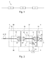
- Figure 1 shows an optical communication system 2.
- the optical communication system 2 is an undersea system.
- the optical communication system 2 is connected upstream and downstream to a communication network, for example a WDM communication network.
- the optical communication system 2 comprises several cascaded optical amplification devices 4. Only three optical amplification devices 4 are shown on Figure 1 , although the optical communication system 2 can include a much larger number of devices, for example the optical communication system can include up to several hundred devices.
- Each optical amplification device 4 comprises at least one input optical fiber 6, at least one output optical fiber 8, and at least one set 10 of at least two amplifier modules 12.
- Each amplifier module 12 comprises at least one semiconductor optical amplifier (SOA) 14.
- SOA semiconductor optical amplifier
- each optical amplification device 4 comprises five input optical fibers 6, five output optical fibers 8 and one set 10 of six amplifier modules 12, each amplifier module 12 comprising one SOA 14.
- Each optical amplification device 4 further comprises means 16 for monitoring the state of each SOA 14, and means 18 for mechanically moving the optical amplification device 4 from a first configuration to at least one second configuration.
- the number of amplifier modules 12 is strictly greater than the number of output optical fiber(s) 8.
- this feature allows reducing the manufacturing costs of the device 4.
- the or each input optical fiber 6 is arranged within a first element 20 and is intended to receive an input optical signal 22.
- the or each output optical fiber 8 is arranged within a second element 24 and is intended to provide an output optical signal 26.
- the or each set 10 of amplifier modules 12 is arranged within a third element 28.
- arranged within any permanent arrangement of a first element towards a second element, may the first element be physically located inside the second member or on an outer surface thereof.
- the optical amplification system 4 comprises one first element 20 within which are arranged the five input optical fibers 6, one second element 24 within which are arranged the five output optical fibers 8, and one third element 28 within which is arranged the set 10 of amplifier modules 12.
- the monitoring means 16 are configured to detect a default or failure of each SOA 14, and to provide a default or failure detection signal 29 of one of the SOA 14.
- the monitoring means 16 comprise for example at least two photodiodes 30. This feature allows to have a high reliability for the detection of a default or failure of the SOA 14.
- the monitoring means 16 comprise six photodiodes 30, even though only one photodiode 30 is shown on Figure 2 for clarity reasons.
- Each photodiode 30 is arranged so as to receive at least part of one of the amplified optical signals provided by an amplifier module 12.
- each photodiode 30 is arranged so as to receive part of one of the amplified optical signals provided by an amplifier module 12, said part of an amplified optical signal being a signal 32 that is for example deflected by a semi-reflecting mirror 33.
- the moving means 18 are connected to the monitoring means 16 so that the moving means 18 are adapted to move the optical amplification device 4 from the first configuration to the or one of the second configuration(s) upon receipt of a default or failure detection signal 29 of one of the SOA 14.
- the or each third element 28 is arranged between the or one of the first element(s) 20 and the or one of the second element(s) 24 so that, in the first configuration of the optical amplification device 4, at least one amplifier module 12 of the set 10 arranged within said third element 28 is on the optical path of one input optical fiber 6 and one output optical fiber 8.
- the optical amplification device 4 is configured so that, in the or each second configuration of the device, for the or one of the third element(s) 28 associated to one set 10 of amplifier modules 12, no more optical signal is injected within the amplifier module 12 comprising the default or failed SOA 14 detected by the monitoring means 16.
- the third element 28 is arranged between the first element 20 and the second element 24 so that, in the first configuration of the optical amplification device 4, there are five amplifier modules 12 of the set 10 arranged within said third element 28 that are each on the optical path of one input optical fiber 6 and one output optical fiber 8, as shown in Figures 3, 4 and 5 .
- the optical amplification device 4 has five second configurations, in each second configuration, for the third element 28 associated to the set 10 of amplifier modules 12, no more optical signal is injected within the amplifier module 12 comprising the default or failed SOA 14, as will be described below in greater details with reference to Figures 6 to 8 .
- the number of amplifier modules 12 of said set 10 is strictly greater than the number of active input optical fiber(s) 6 arranged within the first element 20 that is disposed facing the third element 28 associated to said set 10 of amplifier modules 12.
- the first element 20 of the optical amplification device 4 includes five active input optical fibers 6 in the first configuration of the device, and the third element 28 includes a set 10 of six amplifier modules 12.
- the or one of the amplifier module(s) 12 of said set 10 that was not on the optical path of an active input optical fiber 6 in the first configuration of the device is on the optical path of one active input optical fiber 6 and one output optical fiber 8.
- the moving means 18 may for example comprise a motor-driven rotational axis with predefined positioning cycles.
- At least one of the first and second elements 20, 24 comprises a collimator 34 arranged on a same optical path as that of the or one of the optical fiber(s) 6, 8 that is (are) arranged within said element 20, 24.
- this feature allows correcting divergence of the optical beam and thus reducing transmission loss.
- each of the first and second elements 20, 24 comprises five collimators 34, each collimator 34 of a given element 20, 24 being arranged on a same optical path as that of one of the input or output optical fibers 6, 8 that are arranged within said element 20, 24.
- each collimator 34 includes a lens 36, as shown in the exemplary embodiment of Figure 2 .
- Each lens 36 of a given element 20, 24 is configured to focus light going in or coming from one of the optical fibers 6, 8 that are arranged within said element 20, 24.
- Each of the first and second elements 20, 24 is for example configured as a cylinder.
- the third element 28 is fixed permanently and the first element 20 is a rotating element mounted around a rotation axis.
- the moving means 18 are configured to drive the first element 20 around its rotation axis, so as to move the optical amplification device 4 from the first configuration to each second configuration.
- the second element 24 is also a rotating element mounted around a rotation axis and the moving means 18 are configured to drive the second element 24 around its rotation axis.
- the third element 28 comprises at least one lens 38 arranged upstream or downstream one of the SOA 14, on a same optical path of said SOA 14.
- the or each lens 38 arranged upstream or downstream one of the SOA 14 is configured to focus light going in or coming from said SOA 14.
- the third element 28 comprises twelve lenses 38. More precisely, the third element 28 comprises six first lenses 38 that are each arranged upstream one distinct SOA 14, on a same optical path of said SOA 14, and six other lenses 38 that are each arranged downstream one distinct SOA 14, on a same optical path of said SOA 14.
- the third element 28 is for example configured as a cylinder, said cylinder having a set 10 of six angularly equispaced amplifier modules 12.
- the five input optical fibers 6 are all active input fibers.
- five amplifier modules 12 of the set 10 arranged within the third element 28 are each on the optical path of one input optical fiber 6 and one output optical fiber 8, as shown in Figures 3, 4 and 5 .
- the other amplifier module 12A of the set 10 arranged within the third element 28 is not on the optical path of an active input optical fiber 6.
- the monitoring means 16 When a default or failure of one particular SOA 14A, belonging to one of said five amplifier modules 12, is detected by the monitoring means 16, the monitoring means 16 transmit a default or failure detection signal 29 to the moving means 18.
- the moving means 18 Upon receipt of the default or failure detection signal 29, the moving means 18 move the optical amplification device 4 from the first configuration to one of the second configurations, which is shown in Figures 6 to 8 . More precisely, the moving means 18 move the first and second elements 20, 24 around their respective rotation axis, so as to move the optical amplification device 4 from the first configuration to said second configuration, as shown in Figures 3 and 5 .
- the amplifier module 12 comprising the default or failed SOA 14A. More precisely, the amplifier module 12 comprising the default or failed SOA 14A is no more on the optical path of an active input optical fiber 6. Besides, the amplifier module 12A, that was not on the optical path of an active input optical fiber 6 in the first configuration of the device 4, is now on the optical path of one active input optical fiber 6 and one output optical fiber 8.
- this amplifier module 12A stands for a relief amplifier module that avoids a maintenance work for replacing the amplifier module 12 comprising the default or failed SOA 14A.
- the optical amplification device according to the invention allows amplifying extremely wide optical bandwidth, while being reliable.
- Figure 9 illustrates a second embodiment of the optical amplification device according to the invention wherein elements similar to the first embodiment described above are identified by identical reference numbers and thus are not described again.
- the optical amplification device 4 comprises two pairs of input optical fibers 6, two pairs of output optical fibers 8 and two sets 10A, 10B of amplifier modules 12, each set 10A, 10B having three amplifier modules 12.
- Each amplifier module 12 comprises one SOA 14.
- the first pair of input optical fibers 6 is arranged within a first element 20A, and the other pair of input optical fibers 6 is arranged within another first element 20B.
- the first pair of output optical fibers 8 is arranged within a second element 24A, and the other pair of output optical fibers 8 is arranged within another second element 24B.
- a first set 10A of amplifier modules 12 is arranged within a third element 28A.
- a second set 10B of amplifier modules 12 is arranged within another third element 28B.
- Each third element 28A, 28B is arranged between one first element 20A, 20B and one second element 24A, 24B so that, in the first configuration of the optical amplification device 4, two amplifier modules 12 of the set 10A, 10B arranged within said third element 28A, 28B are each on the optical path of one input optical fiber 6 and one output optical fiber 8, as shown in Figure 9 .
- the optical amplification device 4 has two second configurations per third element 28A, 28B (i.e. four second configurations in total)
- no more optical signal is injected within the amplifier module 12 comprising the default or failed SOA 14.
- each first element 20A, 20B of the optical amplification device 4 includes two active input optical fibers 6 in the first configuration of the device, and each third element 28A, 28B includes a set 10A, 10B of three amplifier modules 12.
- each of the four second configurations of the optical amplification device 4 for the set 10A, 10B of amplifier modules 12 having the amplifier module comprising the default or failed SOA 14, one of the amplifier modules 12 of said set 10A, 10B that was not on the optical path of an active input optical fiber 6 in the first configuration of the device is on the optical path of one active input optical fiber 6 and one output optical fiber 8.
- first elements 20A, 20B and the second elements 24A, 24B are fixed permanently and each third element 28A, 28B is a rotating element mounted around a rotation axis.
- the moving means 18 are configured to drive the third elements 28A, 28B independently around their respective rotation axis, so as to move the optical amplification device 4 from the first configuration to each second configuration.
- the optical amplification device 4 comprises at least two sets of at least two input optical fibers 6, at least two sets of at least two output optical fibers 8, and at least two sets of at least three amplifier modules 12, the input optical fibers 6 of separate sets of input optical fibers being arranged within separate first elements, the output optical fibers 8 of separate sets of output optical fibers being arranged within separate second elements, the amplifier modules 12 of separate sets of amplifier modules being arranged within separate third elements.
- the optical amplification device 4 offers an enhanced reliability, due to the presence of at least one relief amplifier module 12 per set 10A, 10B of amplifier modules 12.
- this second embodiment of the optical amplification device 4 is similar to that of the first embodiment and is therefore not described in greater detail.
- Figure 10 illustrates a third embodiment of the optical amplification device according to the invention wherein elements similar to the first embodiment described above are identified by identical reference numbers and thus are not described again.
- the optical amplification system 4 comprises one first element 20 within which are arranged five input optical fibers 6, one second element 24 within which are arranged five output optical fibers 8, and one third element 28 within which is arranged a set 10 of six amplifier modules 12.
- Each amplifier module 12 comprises two parallel SOA 14.
- Each SOA 14 of a given amplifier module 12 is intended to amplify one particular polarization of the received input optical signal 22.
- Each of the first and second elements 20, 24 comprises five lenses 40, each lens 40 of a given element 20, 24 being arranged on a same optical path as that of one of the input or output optical fibers 6, 8 that are arranged within said element 20, 24.
- the first element 20 comprises five optical polarizers 42, each polarizer 42 being arranged downstream one of the lenses 40 of said first element 20, on a same optical path as that of said lens 40.
- Each polarizer 42 comprises a half waveplate 44 arranged on substantially half of the length of one of its outer faces.
- the second element 24 comprises five optical analyzers 46, each analyzer 46 being arranged upstream one of the lenses 40 of said second element 24, on a same optical path as that of said lens 40.
- Each analyzer 46 comprises a half waveplate 48 arranged on substantially half of the length of one of its outer faces.
- the third element 28 comprises twelve first lenses 38 that are each arranged upstream one distinct SOA 14, on a same optical path of said SOA 14, and twelve second lenses 38 that are each arranged downstream one distinct SOA 14, on a same optical path of said SOA 14.
- Each half waveplate 44 is arranged to face one of the first lenses 38 of the third element 28, so as to provide one particular polarization of the received input optical signal 22 to one of the SOA 14.
- Each half waveplate 48 is arranged to face one of the second lenses 38 of the third element 28, so as to receive one particular polarization of the amplified optical signal provided by one of the SOA 14.
- the optical amplification device 4 according to this third embodiment allows reducing noise while getting enhanced output power. The performances of the optical amplification device 4 are thus increased.
- this third embodiment of the optical amplification device 4 is similar to that of the first embodiment and is therefore not described in greater detail.
- any block diagrams herein represent conceptual views of illustrative circuitry embodying the principles of the invention.
- any flow charts, flow diagrams, state transition diagrams, pseudo code, and the like represent various processes which may be substantially represented in computer readable medium and so executed by a computer or processor, whether or not such computer or processor is explicitly shown.
Landscapes
- Physics & Mathematics (AREA)
- Condensed Matter Physics & Semiconductors (AREA)
- General Physics & Mathematics (AREA)
- Electromagnetism (AREA)
- Optics & Photonics (AREA)
- Optical Communication System (AREA)
Abstract
• at least one input optical fiber (6) arranged within a first element (20),
• at least one output optical fiber (8) arranged within a second element (24),
• at least one set (10) of at least two amplifier modules (12) arranged within a third element (28), each amplifier module (12) comprising at least one semiconductor optical amplifier (14), the or each third element (28) being arranged between the or one of the first element(s) (20) and the or one of the second element(s) (24) so that, in a first configuration of the device (4), at least one amplifier module (12) is on the optical path of one input optical fiber (6) and one output optical fiber (8),
• means (16) for monitoring the state of each semiconductor optical amplifier (14),
• means (18) for mechanically moving the device (4) from the first configuration to at least one second configuration,
the device (4) being configured so that, in the or each second configuration, for the or one of the third element(s) (28) associated to one set of amplifier modules (12), no more optical signal is injected within the amplifier module (12) comprising a default or failed semiconductor optical amplifier (14).
Description
- The present invention generally relates to the field of optical communication networks, in particular to optical amplification devices for optical communication networks. More particularly, but not exclusively, the present invention relates to optical amplification devices adapted for being used in undersea optical communication systems.
- In a typical optical communication network, optical signals are transmitted along optical links (typically, optical fibers) between nodes of the network. Typically, each optical signal results from the digital modulation of the amplitude and/or phase of the light emitted by a light source (such as a laser) included in a transmitter of a node, at a certain wavelength, and it propagates along an optical fiber.
- For increasing the capacity of the optical fiber, it is also known to implement the Wavelength Division Multiplexing (WDM) technique, which consists in transmitting, along a same optical fiber, two or more optical signals onto light carriers having distinct wavelengths.
- In a typical undersea optical communication network, the lengths of the optical links between two successive nodes of the network are extremely high. Thus, some optical amplification devices need to be used in such a network, so as to ensure an efficient propagation of the signal. However, the use of such an optical communication system under the sea involves some access and maintenance constraints. Thus, with the use of such an optical communication system under the sea comes the problem of the reliability of the system.
- Some solutions exist for enhancing the reliability of such an undersea system.
- For example, an optical amplification device has been proposed that comprises two laser-based optical pumps combined with an extremely reliable 3 dB optical coupler. The two optical pumps are used in parallel. The two pumps inject their pumped signal, for each direction of optical transmission, into an Erbium doped fiber. The or each Erbium doped fiber is connected to two optical fibers, via optical couplers, thereby forming an optical transmission path for the optical signals. Thus, no active component is directly on the path of the optical signal. This ensures an excellent reliability of the system. Indeed, failure of one pump induces a loss of 3dB of pump power, hence a small Optical Signal-to-Noise Ratio (OSNR) degradation for the complete line.
- However, such optical amplification devices used in undersea systems do not allow amplifying extremely wide optical bandwidth. Since total capacity of transport in undersea systems is currently approaching the maximum capacity allowed by currently used optical amplification bandwidth, the increase of optical bandwidth becomes mandatory to avoid future capacity bottleneck in undersea systems.
- There is thus a need for a reliable optical amplification device that would allow amplifying extremely wide optical bandwidth.
- So an object of this invention is to provide an optical amplification device allowing to amplify extremely wide optical bandwidth, while being reliable.
- According to a first aspect, the present invention provides an optical amplification device comprising:
- at least one input optical fiber arranged within a first element and intended to receive an input optical signal,
- at least one output optical fiber arranged within a second element and intended to provide an output optical signal,
- at least one set of at least two amplifier modules, the or each set of amplifier modules being arranged within a third element, each amplifier module comprising at least one semiconductor optical amplifier, the or each third element being arranged between the or one of the first element(s) and the or one of the second element(s) so that, in a first configuration of the device, at least one amplifier module of the set arranged within said third element is on the optical path of one input optical fiber and one output optical fiber,
- means for monitoring the state of each semiconductor optical amplifier, said means being configured to detect a default or failure of said semiconductor optical amplifier,
- means for mechanically moving the device from the first configuration to at least one second configuration, said moving means being connected to the monitoring means so that the moving means are adapted to move the device from the first configuration to the second configuration upon receipt of a default or failure detection signal of one of the semiconductor optical amplifiers, the device being configured so that, in the or each second configuration, for the or one of the third element(s) associated to one set of amplifier modules, no more optical signal is injected within the amplifier module comprising the default or failed semiconductor optical amplifier.
- Semiconductor optical amplifiers have the capability to amplify extremely wide optical bandwidth. Besides, with such an advantageous configuration for the amplification device, in case of failure of one semiconductor optical amplifier, the third element or the first and second elements are moved from the first configuration to the second configuration of the device so that to avoid sending any signal in the default or failed semiconductor optical amplifier. Advantageously, with this optical amplification device according to the present invention, at least one semiconductor optical amplifier can fails at each amplification device location without interrupting the optical transmission.
- The optical amplification device may include additional characteristics considered separately or combined, and notably:
- in the first configuration of the device, when an input optical signal is injected within the or at least one of the input optical fiber(s), thereby defining this or these input optical fiber(s) as active input optical fiber(s), for the or each third element associated to one set of amplifier modules, the number of amplifier modules of said set is strictly greater than the number of active input optical fiber(s) arranged within the first element that is disposed facing the third element associated to said set of amplifier modules ;
- in the or each second configuration of the device, for the set of amplifier modules having the amplifier module comprising the default or failed semiconductor optical amplifier, the or one of the amplifier module(s) of said set that was not on the optical path of an active input optical fiber in the first configuration of the device is on the optical path of one active input optical fiber and one output optical fiber;
- each amplifier module comprises two parallel semiconductor optical amplifiers, each semiconductor optical amplifier being intended to amplify one particular polarization of the received input optical signal ;
- the monitoring means comprise at least two photodiodes, each photodiode being arranged so as to receive at least part of one of the amplified optical signals provided by an amplifier module ;
- the or each third element comprises at least one lens arranged upstream or downstream one of the semiconductor optical amplifiers, on a same optical path of said amplifier, said lens being configured to focus light going in or coming from said amplifier;
- at least one of the first and second elements comprises a collimator arranged on a same optical path as that of the or one of the optical fiber(s) that is (are) arranged within said element;
- the collimator includes a lens configured to focus light going in or coming from the or one of the optical fiber(s) that is (are) arranged within said element;
- the number of amplifier modules is strictly greater than the number of output optical fiber(s) ;
- the or each third element is fixed permanently and the or each second element is a rotating element mounted around a rotation axis, the moving means being configured to drive the or each second element around its rotation axis ;
- the device comprises at least two sets of at least two input optical fibers and at least two sets of at least two output optical fibers, the device further comprising at least two sets of at least three amplifier modules, the input optical fibers of separate sets of input optical fibers being arranged within separate first elements, the output optical fibers of separate sets of output optical fibers being arranged within separate second elements, the amplifier modules of separate sets of amplifier modules being arranged within separate third elements ;
- the or each third element is fixed permanently, and the or each first element is a rotating element mounted around a rotation axis, the moving means being configured to drive the or each first element around its rotation axis, so as to move the device from the first configuration to the or each second configuration.
- According to a second aspect, the present invention provides an optical communication system comprising a plurality of cascaded optical amplification devices, wherein each optical amplification device is as set forth above.
- The optical communication system may include the additional feature wherein the optical communication system is an undersea system.
- Some embodiments of apparatus and/or methods in accordance with embodiments of the present invention are now described, by way of example only, and with reference to the accompanying drawings, in which :
- The
Figure 1 schematically and functionally illustrates an optical communication system comprising three optical amplification devices according to the present invention, - The
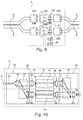
Figure 2 schematically and functionally illustrates one of the optical amplification devices ofFigure 1 according to a first embodiment of the present invention, the device comprising a first element, a second element and a third element, - The
Figures 3 to 5 are respective sectional views, taken respectively along the axes III-III, IV-IV and V-V, of the first, second and third elements of the device ofFigure 2 , in a first configuration of the device, - The
Figures 6 to 8 are respective sectional views, taken respectively along the axes III-III, IV-IV and V-V, of the first, second and third elements of the device ofFigure 2 , in a second configuration of the device, - The
Figure 9 schematically and functionally illustrates one of the optical amplification devices ofFigure 1 according to a second embodiment of the present invention, - The
Figure 10 schematically and functionally illustrates one of the optical amplification devices ofFigure 1 according to a third embodiment of the present invention. -
Figure 1 shows anoptical communication system 2. In the exemplary embodiment ofFigure 1 , theoptical communication system 2 is an undersea system. - The
optical communication system 2 is connected upstream and downstream to a communication network, for example a WDM communication network. Theoptical communication system 2 comprises several cascadedoptical amplification devices 4. Only threeoptical amplification devices 4 are shown onFigure 1 , although theoptical communication system 2 can include a much larger number of devices, for example the optical communication system can include up to several hundred devices. - Each
optical amplification device 4 comprises at least one inputoptical fiber 6, at least one outputoptical fiber 8, and at least oneset 10 of at least twoamplifier modules 12. Eachamplifier module 12 comprises at least one semiconductor optical amplifier (SOA) 14. In the exemplary embodiment ofFigures 2 to 8 , eachoptical amplification device 4 comprises five inputoptical fibers 6, five outputoptical fibers 8 and oneset 10 of sixamplifier modules 12, eachamplifier module 12 comprising oneSOA 14. Eachoptical amplification device 4 further comprises means 16 for monitoring the state of eachSOA 14, and means 18 for mechanically moving theoptical amplification device 4 from a first configuration to at least one second configuration. - Preferably, as shown in
Figures 4, 5, 7 and 8 , the number ofamplifier modules 12 is strictly greater than the number of output optical fiber(s) 8. Advantageously, this feature allows reducing the manufacturing costs of thedevice 4. - The or each input
optical fiber 6 is arranged within afirst element 20 and is intended to receive an inputoptical signal 22. The or each outputoptical fiber 8 is arranged within asecond element 24 and is intended to provide an outputoptical signal 26. The or each set 10 ofamplifier modules 12 is arranged within athird element 28. - By "arranged within" it is meant any permanent arrangement of a first element towards a second element, may the first element be physically located inside the second member or on an outer surface thereof.
- In the exemplary embodiment of
Figures 2 to 8 , theoptical amplification system 4 comprises onefirst element 20 within which are arranged the five inputoptical fibers 6, onesecond element 24 within which are arranged the five outputoptical fibers 8, and onethird element 28 within which is arranged the set 10 ofamplifier modules 12. - The monitoring means 16 are configured to detect a default or failure of each
SOA 14, and to provide a default orfailure detection signal 29 of one of theSOA 14. The monitoring means 16 comprise for example at least twophotodiodes 30. This feature allows to have a high reliability for the detection of a default or failure of theSOA 14. In the exemplary embodiment ofFigures 2 to 8 , the monitoring means 16 comprise sixphotodiodes 30, even though only onephotodiode 30 is shown onFigure 2 for clarity reasons. - Each
photodiode 30 is arranged so as to receive at least part of one of the amplified optical signals provided by anamplifier module 12. In the exemplary embodiment ofFigures 2 to 8 , eachphotodiode 30 is arranged so as to receive part of one of the amplified optical signals provided by anamplifier module 12, said part of an amplified optical signal being asignal 32 that is for example deflected by asemi-reflecting mirror 33. - The moving means 18 are connected to the monitoring means 16 so that the moving means 18 are adapted to move the
optical amplification device 4 from the first configuration to the or one of the second configuration(s) upon receipt of a default orfailure detection signal 29 of one of theSOA 14. - The or each
third element 28 is arranged between the or one of the first element(s) 20 and the or one of the second element(s) 24 so that, in the first configuration of theoptical amplification device 4, at least oneamplifier module 12 of theset 10 arranged within saidthird element 28 is on the optical path of one inputoptical fiber 6 and one outputoptical fiber 8. Besides, theoptical amplification device 4 is configured so that, in the or each second configuration of the device, for the or one of the third element(s) 28 associated to oneset 10 ofamplifier modules 12, no more optical signal is injected within theamplifier module 12 comprising the default or failedSOA 14 detected by the monitoring means 16. In the exemplary embodiment ofFigures 2 to 8 , thethird element 28 is arranged between thefirst element 20 and thesecond element 24 so that, in the first configuration of theoptical amplification device 4, there are fiveamplifier modules 12 of theset 10 arranged within saidthird element 28 that are each on the optical path of one inputoptical fiber 6 and one outputoptical fiber 8, as shown inFigures 3, 4 and 5 . Besides, in this exemplary embodiment wherein theoptical amplification device 4 has five second configurations, in each second configuration, for thethird element 28 associated to theset 10 ofamplifier modules 12, no more optical signal is injected within theamplifier module 12 comprising the default or failedSOA 14, as will be described below in greater details with reference toFigures 6 to 8 . - More precisely, but not necessarily, in the first configuration of the
optical amplification device 4, when an inputoptical signal 22 is injected within the or at least one of the input optical fiber(s) 6, thereby defining this or these input optical fiber(s) 6 as active input optical fiber(s), for the or eachthird element 28 associated to oneset 10 ofamplifier modules 12, the number ofamplifier modules 12 of said set 10 is strictly greater than the number of active input optical fiber(s) 6 arranged within thefirst element 20 that is disposed facing thethird element 28 associated to said set 10 ofamplifier modules 12. In the exemplary embodiment ofFigures 2 to 8 , thefirst element 20 of theoptical amplification device 4 includes five active inputoptical fibers 6 in the first configuration of the device, and thethird element 28 includes aset 10 of sixamplifier modules 12. - Preferably, but not necessarily, in the or each second configuration of the
optical amplification device 4, for theset 10 ofamplifier modules 12 having the amplifier module comprising the default or failedSOA 14, the or one of the amplifier module(s) 12 of said set 10 that was not on the optical path of an active inputoptical fiber 6 in the first configuration of the device is on the optical path of one active inputoptical fiber 6 and one outputoptical fiber 8. In the exemplary embodiment ofFigures 2 to 8 , in each of the five second configurations of theoptical amplification device 4, for theset 10 ofamplifier modules 12 having the amplifier module comprising the default or failedSOA 14, one of theamplifier modules 12 of said set 10 that was not on the optical path of an active inputoptical fiber 6 in the first configuration of the device is on the optical path of one active inputoptical fiber 6 and one outputoptical fiber 8. One of these particular second configurations of theoptical amplification device 4 is for example shown inFigures 6 to 8 . - Though not represented in the Figures for clarity reasons, the moving means 18 may for example comprise a motor-driven rotational axis with predefined positioning cycles.
- Preferably, at least one of the first and
second elements collimator 34 arranged on a same optical path as that of the or one of the optical fiber(s) 6, 8 that is (are) arranged within saidelement Figures 2 to 8 , each of the first andsecond elements collimators 34, eachcollimator 34 of a givenelement optical fibers element - Preferably, each
collimator 34 includes alens 36, as shown in the exemplary embodiment ofFigure 2 . Eachlens 36 of a givenelement optical fibers element - Each of the first and
second elements Figures 2 to 8 , thethird element 28 is fixed permanently and thefirst element 20 is a rotating element mounted around a rotation axis. The moving means 18 are configured to drive thefirst element 20 around its rotation axis, so as to move theoptical amplification device 4 from the first configuration to each second configuration. These last three features allow avoiding power supply constraints for theamplifier modules 12, due for example to wirings. Preferably, as shown inFigures 2 ,5 and 8 , thesecond element 24 is also a rotating element mounted around a rotation axis and the moving means 18 are configured to drive thesecond element 24 around its rotation axis. - Preferably, the
third element 28 comprises at least onelens 38 arranged upstream or downstream one of theSOA 14, on a same optical path of saidSOA 14. The or eachlens 38 arranged upstream or downstream one of theSOA 14 is configured to focus light going in or coming from saidSOA 14. In the exemplary embodiment ofFigures 2 to 8 , thethird element 28 comprises twelvelenses 38. More precisely, thethird element 28 comprises sixfirst lenses 38 that are each arranged upstream onedistinct SOA 14, on a same optical path of saidSOA 14, and sixother lenses 38 that are each arranged downstream onedistinct SOA 14, on a same optical path of saidSOA 14. - The
third element 28 is for example configured as a cylinder, said cylinder having a set 10 of six angularlyequispaced amplifier modules 12. - The operation of the
optical amplification device 4 shown inFigures 2 to 8 , according to the first embodiment of the present invention, will now be described. - Initially, in the first configuration of the
optical amplification device 4, the five inputoptical fibers 6 are all active input fibers. In this first configuration of the device, fiveamplifier modules 12 of theset 10 arranged within thethird element 28 are each on the optical path of one inputoptical fiber 6 and one outputoptical fiber 8, as shown inFigures 3, 4 and 5 . Theother amplifier module 12A of theset 10 arranged within thethird element 28 is not on the optical path of an active inputoptical fiber 6. - When a default or failure of one
particular SOA 14A, belonging to one of said fiveamplifier modules 12, is detected by the monitoring means 16, the monitoring means 16 transmit a default orfailure detection signal 29 to the movingmeans 18. Upon receipt of the default orfailure detection signal 29, the moving means 18 move theoptical amplification device 4 from the first configuration to one of the second configurations, which is shown inFigures 6 to 8 . More precisely, the moving means 18 move the first andsecond elements optical amplification device 4 from the first configuration to said second configuration, as shown inFigures 3 and 5 . - In this second configuration, no more optical signal is injected within the
amplifier module 12 comprising the default or failedSOA 14A. More precisely, theamplifier module 12 comprising the default or failedSOA 14A is no more on the optical path of an active inputoptical fiber 6. Besides, theamplifier module 12A, that was not on the optical path of an active inputoptical fiber 6 in the first configuration of thedevice 4, is now on the optical path of one active inputoptical fiber 6 and one outputoptical fiber 8. - Thus, this
amplifier module 12A stands for a relief amplifier module that avoids a maintenance work for replacing theamplifier module 12 comprising the default or failedSOA 14A. - It is hence conceivable that the optical amplification device according to the invention allows amplifying extremely wide optical bandwidth, while being reliable.
-
Figure 9 illustrates a second embodiment of the optical amplification device according to the invention wherein elements similar to the first embodiment described above are identified by identical reference numbers and thus are not described again. - In the exemplary embodiment of
Figure 9 , theoptical amplification device 4 comprises two pairs of inputoptical fibers 6, two pairs of outputoptical fibers 8 and twosets amplifier modules 12, each set 10A, 10B having threeamplifier modules 12. Eachamplifier module 12 comprises oneSOA 14. - The first pair of input
optical fibers 6 is arranged within afirst element 20A, and the other pair of inputoptical fibers 6 is arranged within anotherfirst element 20B. The first pair of outputoptical fibers 8 is arranged within asecond element 24A, and the other pair of outputoptical fibers 8 is arranged within anothersecond element 24B. Afirst set 10A ofamplifier modules 12 is arranged within athird element 28A. Asecond set 10B ofamplifier modules 12 is arranged within anotherthird element 28B. - Each
third element first element second element optical amplification device 4, twoamplifier modules 12 of the set 10A, 10B arranged within saidthird element optical fiber 6 and one outputoptical fiber 8, as shown inFigure 9 . Besides, in this exemplary embodiment wherein theoptical amplification device 4 has two second configurations perthird element third elements set amplifier modules 12, no more optical signal is injected within theamplifier module 12 comprising the default or failedSOA 14. - More precisely, in the exemplary embodiment of
Figure 9 , eachfirst element optical amplification device 4 includes two active inputoptical fibers 6 in the first configuration of the device, and eachthird element set amplifier modules 12. Besides, in each of the four second configurations of theoptical amplification device 4, for theset amplifier modules 12 having the amplifier module comprising the default or failedSOA 14, one of theamplifier modules 12 of said set 10A, 10B that was not on the optical path of an active inputoptical fiber 6 in the first configuration of the device is on the optical path of one active inputoptical fiber 6 and one outputoptical fiber 8. - In this exemplary embodiment of
Figure 9 , thefirst elements second elements third element third elements optical amplification device 4 from the first configuration to each second configuration. - More generally, the
optical amplification device 4 according to the second embodiment of the invention comprises at least two sets of at least two inputoptical fibers 6, at least two sets of at least two outputoptical fibers 8, and at least two sets of at least threeamplifier modules 12, the inputoptical fibers 6 of separate sets of input optical fibers being arranged within separate first elements, the outputoptical fibers 8 of separate sets of output optical fibers being arranged within separate second elements, theamplifier modules 12 of separate sets of amplifier modules being arranged within separate third elements. - Compared to the first embodiment, the
optical amplification device 4 according to this second embodiment offers an enhanced reliability, due to the presence of at least onerelief amplifier module 12 perset amplifier modules 12. - The operation of this second embodiment of the
optical amplification device 4 is similar to that of the first embodiment and is therefore not described in greater detail. -
Figure 10 illustrates a third embodiment of the optical amplification device according to the invention wherein elements similar to the first embodiment described above are identified by identical reference numbers and thus are not described again. - In this third embodiment, the
optical amplification system 4 comprises onefirst element 20 within which are arranged five inputoptical fibers 6, onesecond element 24 within which are arranged five outputoptical fibers 8, and onethird element 28 within which is arranged aset 10 of sixamplifier modules 12. - Each
amplifier module 12 comprises twoparallel SOA 14. EachSOA 14 of a givenamplifier module 12 is intended to amplify one particular polarization of the received inputoptical signal 22. - Each of the first and
second elements lenses 40, eachlens 40 of a givenelement optical fibers element - Besides, the
first element 20 comprises fiveoptical polarizers 42, eachpolarizer 42 being arranged downstream one of thelenses 40 of saidfirst element 20, on a same optical path as that of saidlens 40. Eachpolarizer 42 comprises ahalf waveplate 44 arranged on substantially half of the length of one of its outer faces. - The
second element 24 comprises fiveoptical analyzers 46, eachanalyzer 46 being arranged upstream one of thelenses 40 of saidsecond element 24, on a same optical path as that of saidlens 40. Eachanalyzer 46 comprises ahalf waveplate 48 arranged on substantially half of the length of one of its outer faces. - The
third element 28 comprises twelvefirst lenses 38 that are each arranged upstream onedistinct SOA 14, on a same optical path of saidSOA 14, and twelvesecond lenses 38 that are each arranged downstream onedistinct SOA 14, on a same optical path of saidSOA 14. - Each
half waveplate 44 is arranged to face one of thefirst lenses 38 of thethird element 28, so as to provide one particular polarization of the received inputoptical signal 22 to one of theSOA 14. Eachhalf waveplate 48 is arranged to face one of thesecond lenses 38 of thethird element 28, so as to receive one particular polarization of the amplified optical signal provided by one of theSOA 14. - Compared to the first embodiment, the
optical amplification device 4 according to this third embodiment allows reducing noise while getting enhanced output power. The performances of theoptical amplification device 4 are thus increased. - The operation of this third embodiment of the
optical amplification device 4 is similar to that of the first embodiment and is therefore not described in greater detail. - It should be appreciated by those skilled in the art that any block diagrams herein represent conceptual views of illustrative circuitry embodying the principles of the invention. Similarly, it will be appreciated that any flow charts, flow diagrams, state transition diagrams, pseudo code, and the like represent various processes which may be substantially represented in computer readable medium and so executed by a computer or processor, whether or not such computer or processor is explicitly shown.
- The description and drawings merely illustrate the principles of the invention. It will thus be appreciated that those skilled in the art will be able to devise various arrangements that, although not explicitly described or shown herein, embody the principles of the invention and are included within its spirit and scope. In particular, although the present description has been made with reference to an undersea optical communication system, the present invention is not limited to this application and can be extended to any kind of optical communication systems, such as for example terrestrial optical communication systems.
- Furthermore, all examples recited herein are principally intended expressly to be only for pedagogical purposes to aid the reader in understanding the principles of the invention and the concepts contributed by the inventor(s) to furthering the art, and are to be construed as being without limitation to such specifically recited examples and conditions. Moreover, all statements herein reciting principles, aspects, and embodiments of the invention, as well as specific examples thereof, are intended to encompass equivalents thereof.
Claims (14)
- Optical amplification device (4) comprising:• at least one input optical fiber (6) arranged within a first element (20 ; 20A, 20B) and intended to receive an input optical signal (22),• at least one output optical fiber (8) arranged within a second element (24 ; 24A, 24B) and intended to provide an output optical signal (26),• at least one set (10 ; 10A, 10B) of at least two amplifier modules (12, 12A), the or each set (10 ; 10A, 10B) of amplifier modules (12, 12A) being arranged within a third element (28 ; 28A, 28B), each amplifier module (12, 12A) comprising at least one semiconductor optical amplifier (14, 14A), the or each third element (28 ; 28A, 28B) being arranged between the or one of the first element(s) (20 ; 20A, 20B) and the or one of the second element(s) (24 ; 24A, 24B) so that, in a first configuration of the device (4), at least one amplifier module (12) of the set (10 ; 10A, 10B) arranged within said third element is on the optical path of one input optical fiber (6) and one output optical fiber (8),• means (16) for monitoring the state of each semiconductor optical amplifier (14, 14A), said means (16) being configured to detect a default or failure of said semiconductor optical amplifier,• means (18) for mechanically moving the device (4) from the first configuration to at least one second configuration, said moving means (18) being connected to the monitoring means (16) so that the moving means (18) are adapted to move the device (4) from the first configuration to the second configuration upon receipt of a default or failure detection signal (29) of one of the semiconductor optical amplifiers (14, 14A),the device (4) being configured so that, in the or each second configuration, for the or one of the third element(s) (28 ; 28A, 28B) associated to one set of amplifier modules (12, 12A), no more optical signal is injected within the amplifier module (12) comprising the default or failed semiconductor optical amplifier (14, 14A).
- Optical amplification device (4) according to claim 1, wherein, in the first configuration of the device, when an input optical signal (22) is injected within the or at least one of the input optical fiber(s) (6), thereby defining this or these input optical fiber(s) (6) as active input optical fiber(s), for the or each third element (28 ; 28A, 28B) associated to one set (10 ; 10A, 10B) of amplifier modules (12, 12A), the number of amplifier modules (12, 12A) of said set is strictly greater than the number of active input optical fiber(s) (6) arranged within the first element (20 ; 20A, 20B) that is disposed facing the third element (28 ; 28A, 28B) associated to said set of amplifier modules (12, 12A).
- Optical amplification device (4) according to claim 2, wherein, in the or each second configuration of the device, for the set (10 ; 10A, 10B) of amplifier modules (12, 12A) having the amplifier module comprising the default or failed semiconductor optical amplifier (14, 14A), the or one of the amplifier module(s) of said set that was not on the optical path of an active input optical fiber in the first configuration of the device is on the optical path of one active input optical fiber (6) and one output optical fiber (8).
- Optical amplification device (4) according to any one of the preceding claims, wherein each amplifier module (12) comprises two parallel semiconductor optical amplifiers (14), each semiconductor optical amplifier (14) being intended to amplify one particular polarization of the received input optical signal (22).
- Optical amplification device (4) according to any one of the preceding claims, wherein the monitoring means (16) comprise at least two photodiodes (30), each photodiode (30) being arranged so as to receive at least part of one of the amplified optical signals provided by an amplifier module (12, 12A).
- Optical amplification device (4) according to any one of the preceding claims, wherein the or each third element (28 ; 28A, 28B) comprises at least one lens (38) arranged upstream or downstream one of the semiconductor optical amplifiers (14, 14A), on a same optical path of said amplifier, said lens (38) being configured to focus light going in or coming from said amplifier.
- Optical amplification device (4) according to any one of the preceding claims, wherein at least one of the first (20 ; 20A, 20B) and second elements (24 ; 24A, 24B) comprises a collimator (34) arranged on a same optical path as that of the or one of the optical fiber(s) (6, 8) that is (are) arranged within said element.
- Optical amplification device (4) according to claim 7, wherein the collimator (34) includes a lens (36) configured to focus light going in or coming from the or one of the optical fiber(s) (6, 8) that is (are) arranged within said element.
- Optical amplification device (4) according to any one of the preceding claims, wherein the number of amplifier modules (12, 12A) is strictly greater than the number of output optical fiber(s) (8).
- Optical amplification device (4) according to claim 9, wherein the or each third element (28 ; 28A, 28B) is fixed permanently and the or each second element (24 ; 24A, 24B) is a rotating element mounted around a rotation axis, the moving means (18) being configured to drive the or each second element (24 ; 24A, 24B) around its rotation axis.
- Optical amplification device (4) according to any one of the preceding claims, wherein the device comprises at least two sets of at least two input optical fibers (6) and at least two sets of at least two output optical fibers (8), the device (4) further comprising at least two sets (10A, 10B) of at least three amplifier modules (12), the input optical fibers (6) of separate sets of input optical fibers being arranged within separate first elements (20A, 20B), the output optical fibers (8) of separate sets of output optical fibers being arranged within separate second elements (24A, 24B), the amplifier modules (12) of separate sets (10A, 10B) of amplifier modules being arranged within separate third elements (28A, 28B).
- Optical amplification device (4) according to any one of the preceding claims, wherein the or each third element (28 ; 28A, 28B) is fixed permanently, and the or each first element (20 ; 20A, 20B) is a rotating element mounted around a rotation axis, the moving means (18) being configured to drive the or each first element (20 ; 20A, 20B) around its rotation axis, so as to move the device (4) from the first configuration to the or each second configuration.
- Optical communication system (2) comprising a plurality of cascaded optical amplification devices (4), wherein each optical amplification device (4) is according to any one of the preceding claims.
- Optical communication system (2) according to claim 13, wherein the optical communication system (2) is an undersea system.
Priority Applications (1)
| Application Number | Priority Date | Filing Date | Title |
|---|---|---|---|
| EP15306082.7A EP3113302B8 (en) | 2015-07-02 | 2015-07-02 | Optical amplification device comprising semiconductor optical amplifiers |
Applications Claiming Priority (1)
| Application Number | Priority Date | Filing Date | Title |
|---|---|---|---|
| EP15306082.7A EP3113302B8 (en) | 2015-07-02 | 2015-07-02 | Optical amplification device comprising semiconductor optical amplifiers |
Publications (3)
| Publication Number | Publication Date |
|---|---|
| EP3113302A1 true EP3113302A1 (en) | 2017-01-04 |
| EP3113302B1 EP3113302B1 (en) | 2018-04-04 |
| EP3113302B8 EP3113302B8 (en) | 2018-05-23 |
Family
ID=53610834
Family Applications (1)
| Application Number | Title | Priority Date | Filing Date |
|---|---|---|---|
| EP15306082.7A Active EP3113302B8 (en) | 2015-07-02 | 2015-07-02 | Optical amplification device comprising semiconductor optical amplifiers |
Country Status (1)
| Country | Link |
|---|---|
| EP (1) | EP3113302B8 (en) |
Cited By (1)
| Publication number | Priority date | Publication date | Assignee | Title |
|---|---|---|---|---|
| US20200162163A1 (en) * | 2018-11-20 | 2020-05-21 | Google Llc | Low signal to noise ratio submarine communication system |
Citations (2)
| Publication number | Priority date | Publication date | Assignee | Title |
|---|---|---|---|---|
| US6747793B1 (en) * | 1999-11-15 | 2004-06-08 | Axsun Technologies, Inc. | System with integrated semiconductor optical amplifier array and switching matrix |
| WO2014129613A1 (en) * | 2013-02-25 | 2014-08-28 | カナレ電気株式会社 | Optical amplifier and laser oscillator |
-
2015
- 2015-07-02 EP EP15306082.7A patent/EP3113302B8/en active Active
Patent Citations (2)
| Publication number | Priority date | Publication date | Assignee | Title |
|---|---|---|---|---|
| US6747793B1 (en) * | 1999-11-15 | 2004-06-08 | Axsun Technologies, Inc. | System with integrated semiconductor optical amplifier array and switching matrix |
| WO2014129613A1 (en) * | 2013-02-25 | 2014-08-28 | カナレ電気株式会社 | Optical amplifier and laser oscillator |
Non-Patent Citations (2)
| Title |
|---|
| AZZAM YASSEEN A ET AL: "A Rotary Electrostatic Micromotor 18 Optical Switch", IEEE JOURNAL OF SELECTED TOPICS IN QUANTUM ELECTRONICS, IEEE SERVICE CENTER, PISCATAWAY, NJ, US, vol. 5, no. 1, 1 February 1999 (1999-02-01), XP011062464, ISSN: 1077-260X * |
| MATIJA DZANKO ET AL: "Availability of all-optical switching fabrics used in optical cross-connects", MIPRO, 2012 PROCEEDINGS OF THE 35TH INTERNATIONAL CONVENTION, IEEE, 21 May 2012 (2012-05-21), pages 568 - 572, XP032201978, ISBN: 978-1-4673-2577-6 * |
Cited By (5)
| Publication number | Priority date | Publication date | Assignee | Title |
|---|---|---|---|---|
| US20200162163A1 (en) * | 2018-11-20 | 2020-05-21 | Google Llc | Low signal to noise ratio submarine communication system |
| WO2020106723A1 (en) * | 2018-11-20 | 2020-05-28 | Google Llc | Low signal to noise ratio submarine communication system |
| CN112425097A (en) * | 2018-11-20 | 2021-02-26 | 谷歌有限责任公司 | Low signal-to-noise ratio radio underwater communication system |
| US11044015B2 (en) | 2018-11-20 | 2021-06-22 | Google Llc | Low signal to noise ratio submarine communication system |
| CN112425097B (en) * | 2018-11-20 | 2024-07-26 | 谷歌有限责任公司 | Low signal-to-noise ratio radio underwater communication system |
Also Published As
| Publication number | Publication date |
|---|---|
| EP3113302B8 (en) | 2018-05-23 |
| EP3113302B1 (en) | 2018-04-04 |
Similar Documents
| Publication | Publication Date | Title |
|---|---|---|
| US9699531B2 (en) | Switchable optical amplifier and optical transmission apparatus | |
| US8335428B2 (en) | Method and system for protection switching | |
| US20150349911A1 (en) | Optical receiver | |
| US9166679B2 (en) | Optical amplification apparatus, method for controlling same, optical receiver station, and optical transmission system | |
| US9641242B2 (en) | Optical communication system, device and method for data processing in an optical network | |
| CN107636988A (en) | Optical link based on WDM comb source with improved optical amplification | |
| CN109155674B (en) | System and method for enhancing reliability in a transport network | |
| US10075257B2 (en) | Optical spatial division multiplexing usable at short reach | |
| US12156310B2 (en) | Optical source switching method and apparatus | |
| US9025955B2 (en) | Amplification apparatus and communication system | |
| WO2023005431A1 (en) | Fault locating method, apparatus, and system | |
| US9124362B2 (en) | Optical amplification stage for OTDR monitoring and related method and system for OTDR monitoring of an optical communication link | |
| CN100512057C (en) | Method and apparatus for sharing pump energy from a single pump arrangement to optical fibers located in different fiber pairs | |
| EP3113302B1 (en) | Optical amplification device comprising semiconductor optical amplifiers | |
| US11362753B2 (en) | Optical node device | |
| WO2019006748A1 (en) | Optical amplification device, optical communication station, and optical communication system | |
| CN111344965B (en) | A submarine network device | |
| KR101008771B1 (en) | Optical amplifier | |
| US6690503B2 (en) | Fault tolerant optical amplifier | |
| CN115967437A (en) | self-healing subsea link | |
| JP4405250B2 (en) | Signal light reflection blocking circuit and optical transmission system | |
| WO2024236556A1 (en) | Method and system for co-packaged optics | |
| JP3591494B2 (en) | Optical direct amplifier |
Legal Events
| Date | Code | Title | Description |
|---|---|---|---|
| PUAI | Public reference made under article 153(3) epc to a published international application that has entered the european phase |
Free format text: ORIGINAL CODE: 0009012 |
|
| STAA | Information on the status of an ep patent application or granted ep patent |
Free format text: STATUS: THE APPLICATION HAS BEEN PUBLISHED |
|
| AK | Designated contracting states |
Kind code of ref document: A1 Designated state(s): AL AT BE BG CH CY CZ DE DK EE ES FI FR GB GR HR HU IE IS IT LI LT LU LV MC MK MT NL NO PL PT RO RS SE SI SK SM TR |
|
| AX | Request for extension of the european patent |
Extension state: BA ME |
|
| STAA | Information on the status of an ep patent application or granted ep patent |
Free format text: STATUS: REQUEST FOR EXAMINATION WAS MADE |
|
| 17P | Request for examination filed |
Effective date: 20170704 |
|
| RBV | Designated contracting states (corrected) |
Designated state(s): AL AT BE BG CH CY CZ DE DK EE ES FI FR GB GR HR HU IE IS IT LI LT LU LV MC MK MT NL NO PL PT RO RS SE SI SK SM TR |
|
| RIC1 | Information provided on ipc code assigned before grant |
Ipc: H01S 5/022 20060101AFI20170913BHEP Ipc: H01S 5/50 20060101ALI20170913BHEP Ipc: H01S 5/068 20060101ALI20170913BHEP Ipc: H01S 5/40 20060101ALI20170913BHEP |
|
| GRAP | Despatch of communication of intention to grant a patent |
Free format text: ORIGINAL CODE: EPIDOSNIGR1 |
|
| STAA | Information on the status of an ep patent application or granted ep patent |
Free format text: STATUS: GRANT OF PATENT IS INTENDED |
|
| INTG | Intention to grant announced |
Effective date: 20171020 |
|
| RIN1 | Information on inventor provided before grant (corrected) |
Inventor name: CHARLET, GABRIEL Inventor name: RENAUDIER, JEREMIE |
|
| GRAS | Grant fee paid |
Free format text: ORIGINAL CODE: EPIDOSNIGR3 |
|
| GRAA | (expected) grant |
Free format text: ORIGINAL CODE: 0009210 |
|
| STAA | Information on the status of an ep patent application or granted ep patent |
Free format text: STATUS: THE PATENT HAS BEEN GRANTED |
|
| AK | Designated contracting states |
Kind code of ref document: B1 Designated state(s): AL AT BE BG CH CY CZ DE DK EE ES FI FR GB GR HR HU IE IS IT LI LT LU LV MC MK MT NL NO PL PT RO RS SE SI SK SM TR |
|
| REG | Reference to a national code |
Ref country code: GB Ref legal event code: FG4D |
|
| REG | Reference to a national code |
Ref country code: CH Ref legal event code: EP |
|
| REG | Reference to a national code |
Ref country code: AT Ref legal event code: REF Ref document number: 986570 Country of ref document: AT Kind code of ref document: T Effective date: 20180415 |
|
| RAP2 | Party data changed (patent owner data changed or rights of a patent transferred) |
Owner name: ALCATEL LUCENT |
|
| REG | Reference to a national code |
Ref country code: DE Ref legal event code: R096 Ref document number: 602015009527 Country of ref document: DE |
|
| REG | Reference to a national code |
Ref country code: IE Ref legal event code: FG4D |
|
| REG | Reference to a national code |
Ref country code: NL Ref legal event code: MP Effective date: 20180404 |
|
| REG | Reference to a national code |
Ref country code: LT Ref legal event code: MG4D |
|
| PG25 | Lapsed in a contracting state [announced via postgrant information from national office to epo] |
Ref country code: NL Free format text: LAPSE BECAUSE OF FAILURE TO SUBMIT A TRANSLATION OF THE DESCRIPTION OR TO PAY THE FEE WITHIN THE PRESCRIBED TIME-LIMIT Effective date: 20180404 |
|
| PG25 | Lapsed in a contracting state [announced via postgrant information from national office to epo] |
Ref country code: BG Free format text: LAPSE BECAUSE OF FAILURE TO SUBMIT A TRANSLATION OF THE DESCRIPTION OR TO PAY THE FEE WITHIN THE PRESCRIBED TIME-LIMIT Effective date: 20180704 Ref country code: FI Free format text: LAPSE BECAUSE OF FAILURE TO SUBMIT A TRANSLATION OF THE DESCRIPTION OR TO PAY THE FEE WITHIN THE PRESCRIBED TIME-LIMIT Effective date: 20180404 Ref country code: PL Free format text: LAPSE BECAUSE OF FAILURE TO SUBMIT A TRANSLATION OF THE DESCRIPTION OR TO PAY THE FEE WITHIN THE PRESCRIBED TIME-LIMIT Effective date: 20180404 Ref country code: AL Free format text: LAPSE BECAUSE OF FAILURE TO SUBMIT A TRANSLATION OF THE DESCRIPTION OR TO PAY THE FEE WITHIN THE PRESCRIBED TIME-LIMIT Effective date: 20180404 Ref country code: SE Free format text: LAPSE BECAUSE OF FAILURE TO SUBMIT A TRANSLATION OF THE DESCRIPTION OR TO PAY THE FEE WITHIN THE PRESCRIBED TIME-LIMIT Effective date: 20180404 Ref country code: NO Free format text: LAPSE BECAUSE OF FAILURE TO SUBMIT A TRANSLATION OF THE DESCRIPTION OR TO PAY THE FEE WITHIN THE PRESCRIBED TIME-LIMIT Effective date: 20180704 Ref country code: ES Free format text: LAPSE BECAUSE OF FAILURE TO SUBMIT A TRANSLATION OF THE DESCRIPTION OR TO PAY THE FEE WITHIN THE PRESCRIBED TIME-LIMIT Effective date: 20180404 Ref country code: LT Free format text: LAPSE BECAUSE OF FAILURE TO SUBMIT A TRANSLATION OF THE DESCRIPTION OR TO PAY THE FEE WITHIN THE PRESCRIBED TIME-LIMIT Effective date: 20180404 |
|
| PG25 | Lapsed in a contracting state [announced via postgrant information from national office to epo] |
Ref country code: LV Free format text: LAPSE BECAUSE OF FAILURE TO SUBMIT A TRANSLATION OF THE DESCRIPTION OR TO PAY THE FEE WITHIN THE PRESCRIBED TIME-LIMIT Effective date: 20180404 Ref country code: RS Free format text: LAPSE BECAUSE OF FAILURE TO SUBMIT A TRANSLATION OF THE DESCRIPTION OR TO PAY THE FEE WITHIN THE PRESCRIBED TIME-LIMIT Effective date: 20180404 Ref country code: HR Free format text: LAPSE BECAUSE OF FAILURE TO SUBMIT A TRANSLATION OF THE DESCRIPTION OR TO PAY THE FEE WITHIN THE PRESCRIBED TIME-LIMIT Effective date: 20180404 Ref country code: GR Free format text: LAPSE BECAUSE OF FAILURE TO SUBMIT A TRANSLATION OF THE DESCRIPTION OR TO PAY THE FEE WITHIN THE PRESCRIBED TIME-LIMIT Effective date: 20180705 |
|
| REG | Reference to a national code |
Ref country code: AT Ref legal event code: MK05 Ref document number: 986570 Country of ref document: AT Kind code of ref document: T Effective date: 20180404 |
|
| PG25 | Lapsed in a contracting state [announced via postgrant information from national office to epo] |
Ref country code: PT Free format text: LAPSE BECAUSE OF FAILURE TO SUBMIT A TRANSLATION OF THE DESCRIPTION OR TO PAY THE FEE WITHIN THE PRESCRIBED TIME-LIMIT Effective date: 20180806 |
|
| REG | Reference to a national code |
Ref country code: DE Ref legal event code: R097 Ref document number: 602015009527 Country of ref document: DE |
|
| PG25 | Lapsed in a contracting state [announced via postgrant information from national office to epo] |
Ref country code: EE Free format text: LAPSE BECAUSE OF FAILURE TO SUBMIT A TRANSLATION OF THE DESCRIPTION OR TO PAY THE FEE WITHIN THE PRESCRIBED TIME-LIMIT Effective date: 20180404 Ref country code: SK Free format text: LAPSE BECAUSE OF FAILURE TO SUBMIT A TRANSLATION OF THE DESCRIPTION OR TO PAY THE FEE WITHIN THE PRESCRIBED TIME-LIMIT Effective date: 20180404 Ref country code: AT Free format text: LAPSE BECAUSE OF FAILURE TO SUBMIT A TRANSLATION OF THE DESCRIPTION OR TO PAY THE FEE WITHIN THE PRESCRIBED TIME-LIMIT Effective date: 20180404 Ref country code: DK Free format text: LAPSE BECAUSE OF FAILURE TO SUBMIT A TRANSLATION OF THE DESCRIPTION OR TO PAY THE FEE WITHIN THE PRESCRIBED TIME-LIMIT Effective date: 20180404 Ref country code: CZ Free format text: LAPSE BECAUSE OF FAILURE TO SUBMIT A TRANSLATION OF THE DESCRIPTION OR TO PAY THE FEE WITHIN THE PRESCRIBED TIME-LIMIT Effective date: 20180404 Ref country code: RO Free format text: LAPSE BECAUSE OF FAILURE TO SUBMIT A TRANSLATION OF THE DESCRIPTION OR TO PAY THE FEE WITHIN THE PRESCRIBED TIME-LIMIT Effective date: 20180404 |
|
| PLBE | No opposition filed within time limit |
Free format text: ORIGINAL CODE: 0009261 |
|
| STAA | Information on the status of an ep patent application or granted ep patent |
Free format text: STATUS: NO OPPOSITION FILED WITHIN TIME LIMIT |
|
| PG25 | Lapsed in a contracting state [announced via postgrant information from national office to epo] |
Ref country code: SM Free format text: LAPSE BECAUSE OF FAILURE TO SUBMIT A TRANSLATION OF THE DESCRIPTION OR TO PAY THE FEE WITHIN THE PRESCRIBED TIME-LIMIT Effective date: 20180404 Ref country code: IT Free format text: LAPSE BECAUSE OF FAILURE TO SUBMIT A TRANSLATION OF THE DESCRIPTION OR TO PAY THE FEE WITHIN THE PRESCRIBED TIME-LIMIT Effective date: 20180404 |
|
| REG | Reference to a national code |
Ref country code: CH Ref legal event code: PL |
|
| 26N | No opposition filed |
Effective date: 20190107 |
|
| PG25 | Lapsed in a contracting state [announced via postgrant information from national office to epo] |
Ref country code: LU Free format text: LAPSE BECAUSE OF NON-PAYMENT OF DUE FEES Effective date: 20180702 Ref country code: MC Free format text: LAPSE BECAUSE OF FAILURE TO SUBMIT A TRANSLATION OF THE DESCRIPTION OR TO PAY THE FEE WITHIN THE PRESCRIBED TIME-LIMIT Effective date: 20180404 |
|
| REG | Reference to a national code |
Ref country code: BE Ref legal event code: MM Effective date: 20180731 |
|
| REG | Reference to a national code |
Ref country code: IE Ref legal event code: MM4A |
|
| PG25 | Lapsed in a contracting state [announced via postgrant information from national office to epo] |
Ref country code: FR Free format text: LAPSE BECAUSE OF NON-PAYMENT OF DUE FEES Effective date: 20180731 Ref country code: IE Free format text: LAPSE BECAUSE OF NON-PAYMENT OF DUE FEES Effective date: 20180702 Ref country code: CH Free format text: LAPSE BECAUSE OF NON-PAYMENT OF DUE FEES Effective date: 20180731 Ref country code: LI Free format text: LAPSE BECAUSE OF NON-PAYMENT OF DUE FEES Effective date: 20180731 |
|
| PG25 | Lapsed in a contracting state [announced via postgrant information from national office to epo] |
Ref country code: BE Free format text: LAPSE BECAUSE OF NON-PAYMENT OF DUE FEES Effective date: 20180731 Ref country code: SI Free format text: LAPSE BECAUSE OF FAILURE TO SUBMIT A TRANSLATION OF THE DESCRIPTION OR TO PAY THE FEE WITHIN THE PRESCRIBED TIME-LIMIT Effective date: 20180404 |
|
| PG25 | Lapsed in a contracting state [announced via postgrant information from national office to epo] |
Ref country code: MT Free format text: LAPSE BECAUSE OF NON-PAYMENT OF DUE FEES Effective date: 20180702 |
|
| PG25 | Lapsed in a contracting state [announced via postgrant information from national office to epo] |
Ref country code: TR Free format text: LAPSE BECAUSE OF FAILURE TO SUBMIT A TRANSLATION OF THE DESCRIPTION OR TO PAY THE FEE WITHIN THE PRESCRIBED TIME-LIMIT Effective date: 20180404 |
|
| PG25 | Lapsed in a contracting state [announced via postgrant information from national office to epo] |
Ref country code: CY Free format text: LAPSE BECAUSE OF FAILURE TO SUBMIT A TRANSLATION OF THE DESCRIPTION OR TO PAY THE FEE WITHIN THE PRESCRIBED TIME-LIMIT Effective date: 20180404 Ref country code: MK Free format text: LAPSE BECAUSE OF NON-PAYMENT OF DUE FEES Effective date: 20180404 Ref country code: HU Free format text: LAPSE BECAUSE OF FAILURE TO SUBMIT A TRANSLATION OF THE DESCRIPTION OR TO PAY THE FEE WITHIN THE PRESCRIBED TIME-LIMIT; INVALID AB INITIO Effective date: 20150702 |
|
| PG25 | Lapsed in a contracting state [announced via postgrant information from national office to epo] |
Ref country code: IS Free format text: LAPSE BECAUSE OF FAILURE TO SUBMIT A TRANSLATION OF THE DESCRIPTION OR TO PAY THE FEE WITHIN THE PRESCRIBED TIME-LIMIT Effective date: 20180804 |
|
| PGFP | Annual fee paid to national office [announced via postgrant information from national office to epo] |
Ref country code: GB Payment date: 20250529 Year of fee payment: 11 |
|
| PGFP | Annual fee paid to national office [announced via postgrant information from national office to epo] |
Ref country code: DE Payment date: 20250604 Year of fee payment: 11 |