EP3110043A1 - Carrier phase estimation at a coherent optical receiver - Google Patents
Carrier phase estimation at a coherent optical receiver Download PDFInfo
- Publication number
- EP3110043A1 EP3110043A1 EP15305959.7A EP15305959A EP3110043A1 EP 3110043 A1 EP3110043 A1 EP 3110043A1 EP 15305959 A EP15305959 A EP 15305959A EP 3110043 A1 EP3110043 A1 EP 3110043A1
- Authority
- EP
- European Patent Office
- Prior art keywords
- phase
- module
- error
- sequence
- estimated
- Prior art date
- Legal status (The legal status is an assumption and is not a legal conclusion. Google has not performed a legal analysis and makes no representation as to the accuracy of the status listed.)
- Withdrawn
Links
- 230000003287 optical effect Effects 0.000 title claims abstract description 48
- 230000001427 coherent effect Effects 0.000 title claims abstract description 13
- 238000001914 filtration Methods 0.000 claims abstract description 46
- 238000012360 testing method Methods 0.000 claims description 45
- 238000006243 chemical reaction Methods 0.000 claims description 14
- 238000000034 method Methods 0.000 claims description 13
- 230000004044 response Effects 0.000 claims description 7
- 238000007476 Maximum Likelihood Methods 0.000 claims description 5
- 238000011156 evaluation Methods 0.000 claims description 5
- 238000010845 search algorithm Methods 0.000 claims description 4
- 230000000694 effects Effects 0.000 claims description 2
- 230000010287 polarization Effects 0.000 description 32
- 238000012545 processing Methods 0.000 description 9
- 238000011084 recovery Methods 0.000 description 8
- YBJHBAHKTGYVGT-ZKWXMUAHSA-N (+)-Biotin Chemical compound N1C(=O)N[C@@H]2[C@H](CCCCC(=O)O)SC[C@@H]21 YBJHBAHKTGYVGT-ZKWXMUAHSA-N 0.000 description 6
- 230000005540 biological transmission Effects 0.000 description 6
- FEPMHVLSLDOMQC-UHFFFAOYSA-N virginiamycin-S1 Natural products CC1OC(=O)C(C=2C=CC=CC=2)NC(=O)C2CC(=O)CCN2C(=O)C(CC=2C=CC=CC=2)N(C)C(=O)C2CCCN2C(=O)C(CC)NC(=O)C1NC(=O)C1=NC=CC=C1O FEPMHVLSLDOMQC-UHFFFAOYSA-N 0.000 description 6
- 230000006870 function Effects 0.000 description 5
- 230000008569 process Effects 0.000 description 5
- 238000012937 correction Methods 0.000 description 3
- 238000013459 approach Methods 0.000 description 2
- 238000004891 communication Methods 0.000 description 2
- 239000006185 dispersion Substances 0.000 description 2
- 230000009467 reduction Effects 0.000 description 2
- 238000005070 sampling Methods 0.000 description 2
- 230000035945 sensitivity Effects 0.000 description 2
- 238000012935 Averaging Methods 0.000 description 1
- 239000000654 additive Substances 0.000 description 1
- 230000000996 additive effect Effects 0.000 description 1
- 238000004458 analytical method Methods 0.000 description 1
- 238000010009 beating Methods 0.000 description 1
- 238000005094 computer simulation Methods 0.000 description 1
- 230000006735 deficit Effects 0.000 description 1
- 238000005516 engineering process Methods 0.000 description 1
- 239000000284 extract Substances 0.000 description 1
- 239000000835 fiber Substances 0.000 description 1
- 230000007246 mechanism Effects 0.000 description 1
- 238000004088 simulation Methods 0.000 description 1
- 230000007704 transition Effects 0.000 description 1
Images




Classifications
-
- H—ELECTRICITY
- H04—ELECTRIC COMMUNICATION TECHNIQUE
- H04B—TRANSMISSION
- H04B10/00—Transmission systems employing electromagnetic waves other than radio-waves, e.g. infrared, visible or ultraviolet light, or employing corpuscular radiation, e.g. quantum communication
- H04B10/60—Receivers
- H04B10/61—Coherent receivers
- H04B10/616—Details of the electronic signal processing in coherent optical receivers
- H04B10/6164—Estimation or correction of the frequency offset between the received optical signal and the optical local oscillator
-
- H—ELECTRICITY
- H04—ELECTRIC COMMUNICATION TECHNIQUE
- H04B—TRANSMISSION
- H04B10/00—Transmission systems employing electromagnetic waves other than radio-waves, e.g. infrared, visible or ultraviolet light, or employing corpuscular radiation, e.g. quantum communication
- H04B10/60—Receivers
- H04B10/61—Coherent receivers
- H04B10/65—Intradyne, i.e. coherent receivers with a free running local oscillator having a frequency close but not phase-locked to the carrier signal
Definitions
- the present invention relates to the field of optical communication networks. More particularly, the present invention relates to the carrier phase recovery at a coherent optical receiver.
- current 100 Gb/s transceivers for optical communication networks employ Polarization-Multiplexed Quadrature-Amplitude-Modulation (PM-QAM) schemes and intra-dyne coherent receivers.
- PM-QAM Polarization-Multiplexed Quadrature-Amplitude-Modulation
- information (digital) data are transmitted using two different polarizations and, for each polarization, over an in-phase component (I-component) and a quadrature component (Q-component) of an optical signal.
- I-component in-phase component
- Q-component quadrature component
- the incoming polarization-multiplexed optical signal is mixed by means of a polarization and phase diversity optical front-end with the signal emitted by a local laser.
- the local laser frequency is not locked to the incoming signal but might slightly differ by a value much smaller than the modulation symbol rate.
- the optical front-end typically comprises a pair of optical 90° hybrids, one for each polarization. Each optical 90° hybrid recovers components of the received optical signal at a corresponding polarization.
- ADC analog-to-digital converter
- the sampled electric signals are digitally processed for channel equalization and demodulation.
- Demodulation includes estimating the residual carrier phase (this operation is typically referred to as “carrier recovery”).
- Carrier recovery is followed by a symbol de-mapper stage, which performs symbol to bit conversion, and by a decoding stage which could be based on a hard-decision forward error correction (FEC).
- FEC hard-decision forward error correction
- phase carrier recovery shows a significant computational complexity which can prevent their practical implementation for high order quadrature amplitude modulation, such as an example, 64-QAM or higher cardinalities.
- the present invention provides a carrier phase estimation apparatus comprising:
- said second phase error estimation module comprises: a conversion module configured to generate a plurality of error phasors each depending on said first estimated phase errors; an average filtering module configured to compute a filtered error phasor from said plurality of error phasors; and a computing module configured to compute from said filtered phasor the second estimated phase error associated with one of said symbols of the sequence.
- said average filtering module is configured to compute the filtered error phasor as an average phasor of the plurality of error phasors.
- said average filtering module is implemented by a FIR filter.
- the second phase error estimation module is configured to implement a Viterbi and Viterbi phase estimation algorithm algorithm.
- the sequence of symbols defines a set of phase values having a first cardinality and said first phase error estimation module is configured to generate the first estimated phase errors by a comparison with a set of test phase values having a second cardinality lower than said first cardinality.
- said first phase error estimation module is configured to implement a Maximum Likelihood Phase Search algorithm.
- the first phase error estimation module preferably comprises: a plurality of test phase blocks structured to provide a plurality of error values and a corresponding plurality of estimated phasors associated with said set of test phase values; a minimum evaluation module structured to determine a minimum error value among said plurality of error values; a selector module configured to provide a selected first estimated phase error associated with an estimated phasor of the plurality of estimated phasors and associated with said minimum error value.
- At least one of the plurality of test phase blocks comprises: a phase rotation module configured to generate a phase rotated phasor by rotating of a test angle an input phasor of said sequence of symbols; a decision block structured to provide from the phase rotated phasor an estimated phasor; a differential module configured to provide a difference value from the phase rotated phasor and the estimated phasor; and a filtering module configured to generate an error value of said of plurality of error values by filtering a plurality of difference values generated by the deferential module and associated with said sequence of symbols.
- the filtering module of at least one of the plurality of test phase blocks is configured to mitigate an effect of noise present on the sequence of symbols on said of plurality of error values.
- said filtering module is a Finite Impulse Response filter.
- the filtering module is a moving average filter or a cascade of moving average filters.
- said first phase error estimation module is configured to operate according to a pilot-based carrier phase estimation and comprises: a complex multiplier configured to multiply said sequence of symbols with pilot symbols and provide a resulting sequence of samples; a filter configured to filter the resulting sequence of symbols to obtain a filtered sequence of samples; a phase extracting module to extract from the filtered sequence of samples said first estimated phase errors.
- the input of the carrier phase estimation apparatus is configured to receive the sequence of symbols according to a PM-QAM format.
- the present invention provides a carrier phase estimation method comprising:
- generating the second estimated phase error comprises: converting said first estimated phase errors into a plurality of error phasors; filtering said plurality of error phasors to obtain a filtered error phasor; computing from said filtered phasor the second estimated phase error associated with a respective symbol of said sequence of symbols.
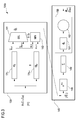
- FIG 1 schematically shows an optical coherent receiver 100 according to embodiments of the present invention.
- the optical coherent receiver 100 is an intra-dyne optical coherent receiver.
- the receiver 100 is preferably configured to receive from a transmitter (not shown in the Figures) an optical signal modulated according to a digital modulation scheme.
- the digital modulation scheme is a PM-QAM (polarization-multiplexed quadrature amplitude modulation) scheme, such as a PM-64QAM scheme.
- PM-QAM polarization-multiplexed quadrature amplitude modulation
- the optical signal is modulated according to a PM-QAM scheme.
- the optical signal is a wavelength-division multiplexed (WDM) signal.
- WDM wavelength-division multiplexed
- the receiver 100 comprises a polarization and phase diversity optical front-end 110 and a digital circuit 130, connected in cascade.
- the optical front-end 110 preferably comprises a filter 111, a local laser 112, a first polarization beam splitter 113, a second polarization beam splitter 114, a first optical 90° hybrid 115, a second optical 90° hybrid 116 and four balanced-photodiodes 117a, 117b, 118a, 118b.
- the receiver 100 in particular its optical front-end 110, particularly receives an incoming optical signal S(t) which carries information symbols with a symbol rate fs.
- the incoming optical signal S(t) is then filtered by the filter 111.
- the filter 111 can be a known channel selector filter. It may select a single wavelength from a WDM signal. Usually it is realized with an array-waveguide grating (AWG) and exhibits Gaussian profile with a bandwidth proportional to the symbol rate (typical ranging from 33GHz to 200GHz). In this particular case, the filter 111 selects a single wavelength ⁇ from the received optical signal S(t).
- AMG array-waveguide grating
- the filtered optical signal is mixed, in the polarization and phase diversity optical front-end 110, with a light beam emitted by the local laser 112.
- the incoming optical signal S(t) has arbitrary polarization, phase and frequency with respect to the local laser 112.
- the local laser frequency is not locked to the incoming signal but might slightly differ by a value much smaller than the symbol rate fs.
- the optical front end 110 separates the incoming signal S(t) into two components associated with two reference polarization axes of the receiver, i.e. two reference polarization axes of the first polarization beam splitter 113.
- Each signal component at the output of the polarization beam splitter 113 is combined with the light beam from the local laser 112 and then separated into two phase-orthogonal components using a 90° hybrid circuit, as it will be described herein after. It is then the task of a digital equalizer and a demodulator in the digital circuit 130 to recover from these four signals the I- and Q-components of the two polarizations of the received signal, as it will be clearer herein after.
- the filtered optical signal S(t) is fed to the first beam splitter 113 and is split into two beams of differing polarizations associated with the reference polarization axes of the receiver, which will be indicated as X, Y. Accordingly, these polarizations are referred to, in the following, as X-polarization and Y-polarization.
- One beam e.g. the X-polarized beam
- the other beam e.g. the Y-polarized beam
- the light beam coming from the local laser 112 is fed to the second beam splitter 114 with 45° polarization angle and is split into two beams of differing polarizations (the same X-polarization and Y-polarization as above).
- One beam (the X-polarized beam) is fed to the first optical 90° hybrid 115 and the other beam (the Y-polarized beam) is fed to the second optical 90° hybrid 116.
- each optical 90° hybrid 115, 116 processes beams of a corresponding polarization.
- Each optical 90° hybrid 115, 116 performs, for the corresponding polarization, the beating between the beam resulting from the splitting of the incoming signal S(t) and the beam resulting from the splitting of the light beam generated by the local laser 112. As known, this leads to separate two phase-orthogonal components of the received optical signal S(t) for each polarization.
- the first optical 90° hybrid 115 recovers phase-orthogonal components of the received optical signal S(t) for the X-polarization and the second optical 90° hybrid 116 recovers phase orthogonal components of the received optical signal S(t) for the Y-polarization.
- the phase-orthogonal components for both polarizations undergo photoelectric conversion within the photodiodes 117a, 117b, 118a, 118b.
- Each photodiode 117a, 117b, 118a, 118b emits an electric signal for the respective component.
- the electric signals associated with the phase-orthogonal components for the X-polarization are emitted by the photodiodes 117a, 117b and indicated as C1x, C2x, while, similarly, the electric signals associated with the phase-orthogonal components for the Y-polarization are emitted by the photodiodes 118a, 118b and indicated as C1y, C2y in Figure 1 .
- the electric signals C1 x, C2x, C1 y, C2y are fed to the digital circuit 130.
- the digital circuit 130 preferably comprises four analog-to-digital converters 131 a, 131b, 132a, 132b and a digital processing unit 133.
- the digital circuit 130 is preferably implemented as a digital signal processor (DSP) inside an application-specific integrated circuit (ASIC).
- DSP digital signal processor
- ASIC application-specific integrated circuit
- the four analog-to-digital converters 131 a, 131b, 132a, 132b preferably process in parallel the electric signals associated with the phase-orthogonal components for the X-polarization, C1x and C2x, and the electric signals associated with the phase-orthogonal components for the Y-polarization, C1y and C2y.
- Each analog-to-digital converter 131 a, 131b, 132a, 132b preferably samples a respective component signal C1x, C2x, C1y, C2y and quantizes the samples so that each sample takes on a value within a finite set, which is determined by the bits of resolution in the analog-to-digital converter 131 a, 131b, 132a, 132b.
- the sequences of quantized samples of the different component signals at the output of the analog-to-digital converters 131 a, 131b, 132a, 132b are indicated in Figure 1 by references C1x(k), C2x(k), C1y(k) and C2y(k), respectively, where k is an integer numerical index indicative of the sampling intervals.
- k is an integer numerical index indicative of the sampling intervals.
- the phase-orthogonal component signals C1x, C2x, and C1y, C2y are sampled at a rate equal to the symbol rate fs or higher.
- FIG. 2 schematically shows a digital processing unit 133 according to an embodiment of the present invention.
- the digital processing unit 133 preferably comprises a channel equalizer 134, a demodulator 135, a de-mapper 137 and a decoder 138.
- the phase orthogonal component samples (or, digital signals) C1x(k), C2x(k) and C1y(k), C2y(k) are fed to the channel equalizer 134.
- the channel equalizer 134 preferably implements known mechanisms for channel equalization, i.e. for compensating transmission impairments such as chromatic dispersion, polarization rotations and polarization mode dispersion (PMD). Therefore, the channel equalizer 134 preferably processes the four digital signals C1x(k), C2x(k) and C1y(k), C2y(k) so that it outputs two complex signals corresponding to the two polarization-multiplexed signals modulated at the transmitter side.
- samples that are sampled at a sampling rate equal to the symbol rate fs are obtained.
- the two complex signals at the channel equalizer output will require demodulation to recover phase and frequency drifts between the local laser 112 and the transmitter laser.
- Demodulation can be performed by two parallel circuits processing each of the two equalizer outputs.
- the channel equalizer 134 is shared by the two polarizations (which are still combined to this point) and then the receiver processes the two polarizations independently and in parallel, each polarization being processed by the demodulator 135, a de-mapper 137 and the decoder 138.
- the demodulator 135 is configured to implement carrier recovery and comprises a frequency estimation block 135a and phase estimation block 135b.
- the frequency estimation block 135a is structured to recover the frequency error between the local laser 112 and the transmitter laser and can operate according to known techniques.
- the phase estimation block 135b is structured to recover the phase error of the local laser 112 with respect to the transmitter laser and the channel, as it will be described in greater detail herein after.
- the demodulator 135, in particular, the phase estimation block 135b, outputs a sequence of demodulated information symbols Zd(k).
- Zd(k) the demodulated information symbols
- the de-mapper 137 is preferably configured to perform symbol decision, i.e. to de-map the incoming symbols into a binary sequence (for hard-decision FEC decoding, or HD-FEC) or into information indicating the reliability of the outcome of symbol decision (for soft-decision FEC decoding, or SD-FEC).
- This information may take the form of a set of log-likelihood ratios (LLRs) associated with the sequence of bits.
- LLRs log-likelihood ratios
- the decoder 138 is preferably configured to implement a forward error correction (FEC) technique.
- the decoder 138 may implement a hard-decision FEC decoding or a soft-decision FEC decoding.
- FIG. 3 shows a particular embodiment of the phase estimation block 135b, which refers to only one of the two polarizations of the polarization-multiplexed signals modulated at the transmitter side: as an example, reference is made to the X-polarization.
- the phase estimation block 135b comprises an input to receive a sequence of symbols ⁇ X n ⁇ corresponding to phasors (i.e. complex electrical signals) having phase-orthogonal components C1x and C2x, as resulting from the channel equalizer 134.
- the phasors associated with symbols ⁇ X n ⁇ define a set of phase values having a cardinality M, i.e. the cardinality of the transmitted PM-QAM signal.
- the first phase estimation block 135b comprises a first phase estimation module 139 and a second phase estimation module 140 (PHASE-EST).
- the first phase estimation module 139 is configured to generate first estimated phase errors ( ⁇ i) associated with the received sequence of symbols ⁇ X n ⁇ .
- the first phase estimation module 139 performs a coarse phase estimation.
- the first phase estimation module 139 is configured to generate estimated phase values ⁇ ⁇ n ⁇ associated with the received sequence of symbols ⁇ X n ⁇ by performing comparison with a set of test phase values ⁇ ⁇ 0 , ... ⁇ b , ... ⁇ B-1 ⁇ having a cardinality, B, lower than the above mentioned cardinality M.
- the estimated phase values ⁇ ⁇ n ⁇ represent corresponding error phase values to be corrected.
- the first phase estimation module 139 is structured to find a coarse estimate of the symbol phase error since it operates with a limited angle resolution.
- the first phase estimation module 139 can be configured according to a Maximum Likelihood Phase Search algorithm (MLPS).
- MLPS Maximum Likelihood Phase Search algorithm
- the second phase estimation module 140 is configured to generate an estimated phase error by an average filtering based on the estimated phase values ⁇ n ⁇ provided by the first phase estimation module 139.
- the second phase estimation module 140 allows to obtain a fine phase estimation and increases the quality of the coarse estimation made by the first phase estimation module 139, by reducing a decision error rate obtainable by the sole first phase estimation module 139.
- average filtering any filtering process which is also capable of attenuating or removing abrupt phase transitions which are, in the present case, associated with the limited angle resolution of the first phase estimation module 139.
- the second phase estimation module 140 comprises a conversion module 148, an average filtering module 149 and an angle computing module 150.
- the angle computing module 150 includes an angle conversion module 151 and an unwrapping module 152.
- the conversion module 148 is configured to generate a plurality of error phasors F n each depending on said first estimated phase values ⁇ ⁇ n ⁇ .
- the average filtering module 149 is configured to compute a filtered error phasor F av from said plurality of error phasors F n and the computing module 150 is configured to extract a second estimated phase error from said filtered error phasor F av .
- the cascade of the conversion module 148,average filtering module 149 and the computing module 150 can be configured to operate according to the Viterbi & Viterbi algorithm as described in A. J. Viterbi and A. M. Viterbi, "Nonlinear estimation of PSK-modulated carrier phase with application to burst digital transmission," IEEE Trans. Inform. Theory, vol. 29, pp. 543-551, Jul. 1983 .
- the phase test phase block TP b comprises a phase rotation module 143, a decision circuit 144 (DEC), a differential node 145, a distance computational module 146 and a filtering module 147.
- the phase rotation module 143 is configured to cause a rotation of a test angle ⁇ b of the corresponding input signal.
- ⁇ b b B - 1 2 ⁇ b ⁇ 0 , 1.... B - 1
- ⁇ is the angular symmetry size of the interval in which the carrier phase error is searched.
- the decision circuit 144 is configured, as an example, to operate by extracting the symbol complex components using combinatorial logic.
- the filtering module 147 can be a Finite Impulse Response (FIR) filter.
- FIR Finite Impulse Response
- the filtering module 147 can be based on block or moving averaging (MA); a moving average filter could employ all equal coefficients.
- MA moving averaging
- the choice of the taps length of the FIR filter of the filtering module 147 depends on the laser linewidth times symbol rate product.
- a symbol X n is supplied to the first phase estimation module 139, as shown in Figure 3 , which operates by searching the phase angle corresponding to the minimum filtered error value computed over the B different test angles.
- the plurality test phase blocks TP 0 -TP B-1 receive the symbol X n .
- the b-th test phase block TP b ( Figure 4 ) it receives the symbol X n which is rotated by the test angle ⁇ b and is fed into the decision circuit 144.
- the computational module 146 computes in the complex plane a distance (e.g. absolute/norm distance or squared distance) to the closest constellation point.
- a distance e.g. absolute/norm distance or squared distance
- the filtering module 147 which mitigates the impact of the noise present on the input signals X n and produces a filtered error value e n,b .
- Each test phase block TP 0 -TP B-1 provides a corresponding filtered error value e n, 0 , ...e n,b ,...e n , B- 1 to the minimum evaluation module 142 and a corresponding estimated phasor X ⁇ n,0 ,... X ⁇ n,b , ... X ⁇ n,B-1 : to the selector module 141 ( Figure 3 ).
- the minimum evaluation module 142 determines the minimum error among the ones provided by the test phase blocks TP 0 -TP B-1 and sends a corresponding selection signal Sd to the selector module 141 which selects a corresponding estimated phasor X ⁇ n .
- the selector module 141 outputs a phase angle ⁇ n , representing an error phase, associated with the selected estimated phasor X ⁇ n .
- the first phase estimation module 139 With reference to consecutive input symbols ⁇ X i ⁇ , the first phase estimation module 139 generates as above described a plurality of estimated phase angles ⁇ ⁇ i (including the particular estimated phase angle ⁇ n ), each representing an estimated phase obtained for the corresponding symbol at the input of the phase estimation block 135b, in a manner analogous to the one above described with reference to estimated phase angle ⁇ n .
- the estimated phase angles according to expression (3) are provided to the second phase estimation module 140, which operates to complete the coarse phase estimation made by the first phase estimation module 139.
- the factor S is equal to 4.
- the factor S is equal to 2.
- the average filtering module 149 can be implemented by a sliding-block approach.
- the angle conversion module 151 extracts the estimated phase angle ⁇ n from the average phasor F av and multiplies it by the factor S so obtaining a phase value S ⁇ n , which falls in an angular range: (- 45°, 45° ] or (- 90° , 90° ] depending on S.
- the unwrapping module 152 expresses the estimated phase angle S ⁇ n in to the range (-180°:180°], so providing the estimated phase error ⁇ e - n for the input symbol X n which can be subtracted from the input signal phase to obtain the sequence of demodulated information symbols Zd(k). It is observed that the multiplication by the factor S gives rise to an S-fold ambiguity in the phase estimate which can be resolved by differential encoding.
- the first phase estimation module 139 is configured to perform the coarse carrier phase estimation by operating according to a pilot-based scheme.
- the first phase estimation module 139 designed according to a pilot-based scheme, is shown in Figure 8 and comprises a complex multiplier 160, a filter 161 and a phase extracting module 162.
- the filter 161 is preferably a moving average interpolation filter.
- the complex multiplier 160 is configured to multiply the incoming symbols X n with the complex conjugate of a symbol sequence P n .
- the symbol sequence P n includes pilot symbols whose value is known at the receiver 100. Pilot symbols are time interleaved with information symbols to generate the transmitted signal. The position of pilot symbols within the received symbol sequence is also known at the receiver.
- the symbol sequence P n can be a zero-padded sequence comprising zeros in time intervals corresponding to non-pilot symbol transmission.
- the pilot symbol periodicity is N
- each pilot symbol occurs at a discrete time instant i ⁇ N, where i is an integer number equal to or higher than 0.
- P n 0 for n ⁇ i ⁇ N
- X n is the symbol sequence at the transmitter side.
- phase estimation block 135b allows performing phase carrier recovery by a reduced computational complexity in comparison with the known techniques and offering satisfying phase noise tolerance and sensitivity performance.
- a further computational complexity reduction is connected to the fact that the average filtering module 149 is shared by all the test phase blocks TP 0 -TP B-1 .
- phase estimation correction apparatus 135b is less complex than known estimators employing Maximum Likelihood algorithm since the fine phase estimation performed by the computing module 150 is performed on the symbol phase errors, provided by the first phase estimation module 139, and is not performed directly on the received modulated symbols.
- the Applicant has carried out computer simulations to analyse performances and characteristics of the phase estimation block 135b including the average filtering module implemented in accordance with the equation (5).
- Figure 5 shows the bit-error ratio (BER) for differentially encoded 64QAM transmission, resulting from comparing three different cases.
- the first case (line “64-MLPS”) refers to the known MLPS algorithm operated with 64 test phase angles and in which the MLPS phase error is computed using the square distance (SD) metrics.
- line "16-MLPS (SD)-post-filter” refers to the described phase estimation block 135b with 16 test phase angles and in which the MLPS the phase error is computed using the square distance (SD) metrics.
- line "16-MLPS (ND)+post-filter” refers to the described phase estimation block 135b with 16 test phase angles and in which the MLPS the phase error is computed using the simpler absolute distance or norm distance (ND) metrics.
- each of the 64 test-angle filters is based on the two-stage MA filter as in equation (2), while in the second and third case each of the 16 test-angle filters is based on a single-stage MA filter.
- Figure 6 shows the Q factor penalty as a function of the linewidth times symbol duration product ( ⁇ fTs) for three different cases, assuming an SNR of 12dB.
- the first case (line “64-MLPS”) refers to the known MLPS algorithm operated with 64 test phase angles each employing a single MA filter.
- the second case (line "64-MLPS 2-stage filter) refers to the known MLPS algorithm operated with 64 test phase angles each employing a two-stage MA filter as in equation (2).
- line "16-MLPS+post-filter” refers to the described phase estimation block 135b with 16 test phase angles each employing a single MA filter.
- the filter block length is optimized for each different linewidth value independently for each investigated case.
- the use of cascaded filter better suits the frequency response of the laser phase noise, leading to larger phase noise tolerance.
- the configuration of the described phase estimation block 135b (line "16-MLPS+post-filter”) performs as the MLPS algorithm operating with 64 test phase filters with two-stage MA filter architecture.
- a penalty lower than 0.1 dB occurs at ⁇ fTs much smaller than 10 -5 , which at 40GBaud corresponds to a input laser linewidth close to 100kHz, which is hardly achievable with commercially available WDM tunable lasers.
- significant linewidth broadening is to be expected after transmission due to fiber non-linearity.
- Figure 7 shows the filter size corresponding to the results plotted in Figure 5 and 6 , which is the optimum filter size to achieve the lowest BER as a function of the linewidth times symbol duration product at an SNR of 12dB.
- the plot reports the length of the combined impulse response.
- the size of average filtering module 149 depends on the frequency content of phase noise and follows the same behavior of the test-angles filters for the known MLPS configuration. It is evident that the use of the average filtering module 149 reduces significantly the size of the parallel test-angle filters with respect to the known MLPS algorithm especially at low phase noise, at the cost of introducing a single stage of filtering after the MLPS decision which is shared among all test angle cases. This leads to a significant computational reduction as each test phase requires a dedicated test-angle filter to compute the MLPS phase search.
- any functional blocks referred to as “device”, “unit”, “block”, “module”, “circuit” or “processing unit” may be provided through the use of dedicated hardware as well as hardware capable of executing software in association with appropriate software.
- the functions may be provided by a single dedicated processor, by a single shared processor, or by a plurality of individual processors, some of which may be shared.
- processing unit should not be construed to refer exclusively to hardware capable of executing software, and may implicitly include, without limitation, digital signal processor (DSP) hardware, network processor, application specific integrated circuit (ASIC), field programmable gate array (FPGA), read only memory (ROM) for storing software, random access memory (RAM), and non volatile storage.
- DSP digital signal processor
- ASIC application specific integrated circuit
- FPGA field programmable gate array
- ROM read only memory
- RAM random access memory
- non volatile storage Other hardware, conventional and/or custom, may also be included.
Landscapes
- Physics & Mathematics (AREA)
- Electromagnetism (AREA)
- Engineering & Computer Science (AREA)
- Computer Networks & Wireless Communication (AREA)
- Signal Processing (AREA)
- Digital Transmission Methods That Use Modulated Carrier Waves (AREA)
Abstract
It is disclosed a carrier phase estimation apparatus (135b) comprising: an input connectable to a digital module (134) of a coherent optical receiver (100) to receive a sequence of symbols (Xi ) representable by phasors; a first phase error estimation module (139) configured to generate first estimated phase errors (ϕ̂ i) associated with said sequence of symbols by performing; a second phase error estimation module (140) configured to generate a second estimated phase error (φe-n ) by an average filtering based on said first estimated phase errors (ϕ̂ i).
Description
- The present invention relates to the field of optical communication networks. More particularly, the present invention relates to the carrier phase recovery at a coherent optical receiver.
- As known, current 100 Gb/s transceivers for optical communication networks employ Polarization-Multiplexed Quadrature-Amplitude-Modulation (PM-QAM) schemes and intra-dyne coherent receivers.
- According to a PM-QAM scheme, information (digital) data are transmitted using two different polarizations and, for each polarization, over an in-phase component (I-component) and a quadrature component (Q-component) of an optical signal.
- In an intra-dyne receiver, the incoming polarization-multiplexed optical signal is mixed by means of a polarization and phase diversity optical front-end with the signal emitted by a local laser. The local laser frequency is not locked to the incoming signal but might slightly differ by a value much smaller than the modulation symbol rate. The optical front-end typically comprises a pair of optical 90° hybrids, one for each polarization. Each optical 90° hybrid recovers components of the received optical signal at a corresponding polarization.
- The components then undergo photoelectric conversion and are mapped into electric signals. The next stage is to convert the electric (analog) signal into digital signals. This is performed by an analog-to-digital converter (ADC), which comprises a sampler that samples the electric signals at a rate equal to or higher than the symbol rate used by the transmitter.
- The sampled electric signals are digitally processed for channel equalization and demodulation. Demodulation includes estimating the residual carrier phase (this operation is typically referred to as "carrier recovery").
- Carrier recovery is followed by a symbol de-mapper stage, which performs symbol to bit conversion, and by a decoding stage which could be based on a hard-decision forward error correction (FEC).
- The inventors noticed that the known schemes for phase carrier recovery show a significant computational complexity which can prevent their practical implementation for high order quadrature amplitude modulation, such as an example, 64-QAM or higher cardinalities.
- In view of the above, it is an object of the present invention to provide an apparatus and a method for phase carrier recovery which show a reduced computational complexity together with satisfying performances, such as an example, phase noise tolerance and sensitivity performance.
- According to a first aspect, the present invention provides a carrier phase estimation apparatus comprising:
- an input connectable to a digital module of a coherent optical receiver to receive a sequence of symbols representable by phasors;
- a first phase error estimation module configured to generate first estimated phase errors associated with said sequence of symbols;
- a second phase error estimation module configured to generate a second estimated phase error by an average filtering based on said first estimated phase errors.
- Preferably, said second phase error estimation module comprises: a conversion module configured to generate a plurality of error phasors each depending on said first estimated phase errors; an average filtering module configured to compute a filtered error phasor from said plurality of error phasors; and a computing module configured to compute from said filtered phasor the second estimated phase error associated with one of said symbols of the sequence.
- Particularly, said average filtering module is configured to compute the filtered error phasor as an average phasor of the plurality of error phasors. As an example, said average filtering module is implemented by a FIR filter. Preferably, the second phase error estimation module is configured to implement a Viterbi and Viterbi phase estimation algorithm algorithm.
- In accordance with a first embodiment, the sequence of symbols defines a set of phase values having a first cardinality and said first phase error estimation module is configured to generate the first estimated phase errors by a comparison with a set of test phase values having a second cardinality lower than said first cardinality. Preferably, said first phase error estimation module is configured to implement a Maximum Likelihood Phase Search algorithm.
- According to a particular example of said first embodiment, when a Maximum Likelihood Phase Search algorithm the first phase error estimation module preferably comprises: a plurality of test phase blocks structured to provide a plurality of error values and a corresponding plurality of estimated phasors associated with said set of test phase values; a minimum evaluation module structured to determine a minimum error value among said plurality of error values; a selector module configured to provide a selected first estimated phase error associated with an estimated phasor of the plurality of estimated phasors and associated with said minimum error value.
- In accordance with a particular embodiment, at least one of the plurality of test phase blocks comprises: a phase rotation module configured to generate a phase rotated phasor by rotating of a test angle an input phasor of said sequence of symbols; a decision block structured to provide from the phase rotated phasor an estimated phasor; a differential module configured to provide a difference value from the phase rotated phasor and the estimated phasor; and a filtering module configured to generate an error value of said of plurality of error values by filtering a plurality of difference values generated by the deferential module and associated with said sequence of symbols.
- Preferably, the filtering module of at least one of the plurality of test phase blocks is configured to mitigate an effect of noise present on the sequence of symbols on said of plurality of error values. Particularly, said filtering module is a Finite Impulse Response filter. More particularly, the filtering module is a moving average filter or a cascade of moving average filters.
- In accordance with a second embodiment, said first phase error estimation module is configured to operate according to a pilot-based carrier phase estimation and comprises: a complex multiplier configured to multiply said sequence of symbols with pilot symbols and provide a resulting sequence of samples; a filter configured to filter the resulting sequence of symbols to obtain a filtered sequence of samples; a phase extracting module to extract from the filtered sequence of samples said first estimated phase errors.
- Preferably, the input of the carrier phase estimation apparatus is configured to receive the sequence of symbols according to a PM-QAM format.
- According to a second aspect, the present invention provides a carrier phase estimation method comprising:
- receiving from a digital module of a coherent optical receiver a sequence of symbols representable by phasors;
- generating first estimated phase errors associated with said sequence of symbols;
- generating a second estimated phase error by an average filtering based on said first estimated phase errors.
- Preferably, generating the second estimated phase error comprises: converting said first estimated phase errors into a plurality of error phasors; filtering said plurality of error phasors to obtain a filtered error phasor; computing from said filtered phasor the second estimated phase error associated with a respective symbol of said sequence of symbols.
- The present invention will become clearer by reading the following detailed description, given by way of example and not of limitation, to be read by referring to the accompanying drawings, wherein:
-
Figure 1 schematically shows an optical coherent receiver according to embodiments of the present invention; -
Figure 2 schematically shows a digital processing unit for the optical coherent receiver ofFigure 1 according to an embodiment of the present invention; -
Figure 3 schematically shows an embodiment of a phase estimation block employable in said digital processing unit and comprising a first phase estimation module and a secondphase estimation module 140; -
Figure 4 schematically shows a first embodiment of a test phase block implementable in said phase estimation block; -
Figure 5 shows bit-error ratio (BER) for differentially encoded 64QAM transmission, resulting from comparing by simulation three different cases; -
Figure 6 shows the Q factor penalty as a function of the linewidth times symbol duration product (ΔfTs) for three different simulated cases; -
Figure 7 shows the filter size for three different phase carrier recovery implementations; -
Figure 8 shows a second embodiment of a test phase block implementable in said phase estimation block; -
Figure 1 schematically shows an opticalcoherent receiver 100 according to embodiments of the present invention. Particularly, the opticalcoherent receiver 100 is an intra-dyne optical coherent receiver. - The
receiver 100 is preferably configured to receive from a transmitter (not shown in the Figures) an optical signal modulated according to a digital modulation scheme. As an example, the digital modulation scheme is a PM-QAM (polarization-multiplexed quadrature amplitude modulation) scheme, such as a PM-64QAM scheme. In the following, for sake of non limiting example, it is assumed that the optical signal is modulated according to a PM-QAM scheme. Preferably, the optical signal is a wavelength-division multiplexed (WDM) signal. - In accordance with the example described, the
receiver 100 comprises a polarization and phase diversity optical front-end 110 and adigital circuit 130, connected in cascade. The optical front-end 110 preferably comprises afilter 111, alocal laser 112, a firstpolarization beam splitter 113, a secondpolarization beam splitter 114, a first optical 90°hybrid 115, a second optical 90°hybrid 116 and four balanced-photodiodes - In operative conditions, the
receiver 100, in particular its optical front-end 110, particularly receives an incoming optical signal S(t) which carries information symbols with a symbol rate fs. The incoming optical signal S(t) is then filtered by thefilter 111. Thefilter 111 can be a known channel selector filter. It may select a single wavelength from a WDM signal. Usually it is realized with an array-waveguide grating (AWG) and exhibits Gaussian profile with a bandwidth proportional to the symbol rate (typical ranging from 33GHz to 200GHz). In this particular case, thefilter 111 selects a single wavelength λ from the received optical signal S(t). - Then, at the output of the
filter 111, the filtered optical signal is mixed, in the polarization and phase diversity optical front-end 110, with a light beam emitted by thelocal laser 112. - It is to be noticed that typically the incoming optical signal S(t) has arbitrary polarization, phase and frequency with respect to the
local laser 112. In particular, the local laser frequency is not locked to the incoming signal but might slightly differ by a value much smaller than the symbol rate fs. The opticalfront end 110 separates the incoming signal S(t) into two components associated with two reference polarization axes of the receiver, i.e. two reference polarization axes of the firstpolarization beam splitter 113. Each signal component at the output of thepolarization beam splitter 113 is combined with the light beam from thelocal laser 112 and then separated into two phase-orthogonal components using a 90° hybrid circuit, as it will be described herein after. It is then the task of a digital equalizer and a demodulator in thedigital circuit 130 to recover from these four signals the I- and Q-components of the two polarizations of the received signal, as it will be clearer herein after. - In particular, the filtered optical signal S(t) is fed to the
first beam splitter 113 and is split into two beams of differing polarizations associated with the reference polarization axes of the receiver, which will be indicated as X, Y. Accordingly, these polarizations are referred to, in the following, as X-polarization and Y-polarization. One beam (e.g. the X-polarized beam) is fed to the first optical 90°hybrid 115 and the other beam (e.g. the Y-polarized beam) is fed to the second optical 90°hybrid 116. Similarly, the light beam coming from thelocal laser 112 is fed to thesecond beam splitter 114 with 45° polarization angle and is split into two beams of differing polarizations (the same X-polarization and Y-polarization as above). One beam (the X-polarized beam) is fed to the first optical 90°hybrid 115 and the other beam (the Y-polarized beam) is fed to the second optical 90°hybrid 116. In other words, each optical 90°hybrid - Each optical 90°
hybrid local laser 112. As known, this leads to separate two phase-orthogonal components of the received optical signal S(t) for each polarization. In particular, the first optical 90°hybrid 115 recovers phase-orthogonal components of the received optical signal S(t) for the X-polarization and the second optical 90°hybrid 116 recovers phase orthogonal components of the received optical signal S(t) for the Y-polarization. - The phase-orthogonal components for both polarizations undergo photoelectric conversion within the
photodiodes photodiode photodiodes photodiodes Figure 1 . After photoelectric conversion the electric signals C1 x, C2x, C1 y, C2y are fed to thedigital circuit 130. - The
digital circuit 130 preferably comprises four analog-to-digital converters digital processing unit 133. Thedigital circuit 130 is preferably implemented as a digital signal processor (DSP) inside an application-specific integrated circuit (ASIC). - The four analog-to-
digital converters digital converter digital converter digital converters Figure 1 by references C1x(k), C2x(k), C1y(k) and C2y(k), respectively, where k is an integer numerical index indicative of the sampling intervals. Preferably the phase-orthogonal component signals C1x, C2x, and C1y, C2y are sampled at a rate equal to the symbol rate fs or higher. -
Figure 2 schematically shows adigital processing unit 133 according to an embodiment of the present invention. Thedigital processing unit 133 preferably comprises achannel equalizer 134, ademodulator 135, a de-mapper 137 and adecoder 138. - In operative conditions, after analog-to-digital conversion, the phase orthogonal component samples (or, digital signals) C1x(k), C2x(k) and C1y(k), C2y(k) are fed to the
channel equalizer 134. Thechannel equalizer 134 preferably implements known mechanisms for channel equalization, i.e. for compensating transmission impairments such as chromatic dispersion, polarization rotations and polarization mode dispersion (PMD). Therefore, thechannel equalizer 134 preferably processes the four digital signals C1x(k), C2x(k) and C1y(k), C2y(k) so that it outputs two complex signals corresponding to the two polarization-multiplexed signals modulated at the transmitter side. Moreover, after channel equalization, samples that are sampled at a sampling rate equal to the symbol rate fs are obtained. The two complex signals at the channel equalizer output will require demodulation to recover phase and frequency drifts between thelocal laser 112 and the transmitter laser. Demodulation can be performed by two parallel circuits processing each of the two equalizer outputs. - With reference to the block scheme of
Figure 2 , it is appreciated that thechannel equalizer 134 is shared by the two polarizations (which are still combined to this point) and then the receiver processes the two polarizations independently and in parallel, each polarization being processed by thedemodulator 135, a de-mapper 137 and thedecoder 138. - In accordance with the described example, the
demodulator 135 is configured to implement carrier recovery and comprises a frequency estimation block 135a andphase estimation block 135b. The frequency estimation block 135a is structured to recover the frequency error between thelocal laser 112 and the transmitter laser and can operate according to known techniques. Thephase estimation block 135b is structured to recover the phase error of thelocal laser 112 with respect to the transmitter laser and the channel, as it will be described in greater detail herein after. - An exemplary known algorithm for frequency estimation is described in A. Leven, et al., "Frequency estimation in intradyne reception" IEEE, Photonics Technology Letters, vol. 19, 2007, pp. 366-368.
- The
demodulator 135, in particular, thephase estimation block 135b, outputs a sequence of demodulated information symbols Zd(k). In the following description, only one polarization will be considered, since processing of the demodulated symbols related to the other polarization is similar. - The de-mapper 137 is preferably configured to perform symbol decision, i.e. to de-map the incoming symbols into a binary sequence (for hard-decision FEC decoding, or HD-FEC) or into information indicating the reliability of the outcome of symbol decision (for soft-decision FEC decoding, or SD-FEC). This information may take the form of a set of log-likelihood ratios (LLRs) associated with the sequence of bits.
- The
decoder 138 is preferably configured to implement a forward error correction (FEC) technique. Thedecoder 138, in particular, may implement a hard-decision FEC decoding or a soft-decision FEC decoding. -
Figure 3 shows a particular embodiment of thephase estimation block 135b, which refers to only one of the two polarizations of the polarization-multiplexed signals modulated at the transmitter side: as an example, reference is made to the X-polarization. - In accordance with the described embodiment, the
phase estimation block 135b comprises an input to receive a sequence of symbols {Xn } corresponding to phasors (i.e. complex electrical signals) having phase-orthogonal components C1x and C2x, as resulting from thechannel equalizer 134. The phasors associated with symbols {Xn } define a set of phase values having a cardinality M, i.e. the cardinality of the transmitted PM-QAM signal. - The first
phase estimation block 135b comprises a firstphase estimation module 139 and a second phase estimation module 140 (PHASE-EST). The firstphase estimation module 139 is configured to generate first estimated phase errors (ϕ̂i) associated with the received sequence of symbols {Xn }. Preferably the firstphase estimation module 139 performs a coarse phase estimation. - In accordance with a first embodiment, the first
phase estimation module 139 is configured to generate estimated phase values {ϕ̂ n} associated with the received sequence of symbols {Xn } by performing comparison with a set of test phase values {ϕ0, ...ϕb, ...ϕB-1 } having a cardinality, B, lower than the above mentioned cardinality M. The estimated phase values {ϕ̂ n} represent corresponding error phase values to be corrected. The firstphase estimation module 139 is structured to find a coarse estimate of the symbol phase error since it operates with a limited angle resolution. In accordance with an example, the firstphase estimation module 139 can be configured according to a Maximum Likelihood Phase Search algorithm (MLPS). - The second
phase estimation module 140 is configured to generate an estimated phase error by an average filtering based on the estimated phase values {ϕ̂n} provided by the firstphase estimation module 139. Preferably, the secondphase estimation module 140 allows to obtain a fine phase estimation and increases the quality of the coarse estimation made by the firstphase estimation module 139, by reducing a decision error rate obtainable by the sole firstphase estimation module 139. - With the term "average filtering" is meant any filtering process which is also capable of attenuating or removing abrupt phase transitions which are, in the present case, associated with the limited angle resolution of the first
phase estimation module 139. - In accordance with an example, the second
phase estimation module 140 comprises aconversion module 148, anaverage filtering module 149 and anangle computing module 150. As an example, theangle computing module 150 includes anangle conversion module 151 and anunwrapping module 152. - The
conversion module 148 is configured to generate a plurality of error phasors Fn each depending on said first estimated phase values {ϕ̂ n}. Theaverage filtering module 149 is configured to compute a filtered error phasor Fav from said plurality of error phasors Fn and thecomputing module 150 is configured to extract a second estimated phase error from said filtered error phasor Fav. - In accordance with a preferred embodiment, the cascade of the
conversion module 148,average filtering module 149 and thecomputing module 150 can be configured to operate according to the Viterbi & Viterbi algorithm as described in A. J. Viterbi and A. M. Viterbi, "Nonlinear estimation of PSK-modulated carrier phase with application to burst digital transmission," IEEE Trans. Inform. Theory, vol. 29, pp. 543-551, Jul. 1983. - In accordance with the particular example shown in
Figure 3 , the firstphase estimation module 139 is structured to operate according a MLPS technique and is provided with a plurality of test phase blocks TP0-TPB-1, a selector module 141 (SEL) and a minimum evaluation module 142 (MIN). It is observed that the number B of the test phase blocks TB0-TPB-1 is lower than the cardinality M of the transmitted PM-QAM signal. As an example, for PM-64-QAM transmitted signals the number of the test phase blocks TB0-TPB-1 can be B =16. - An example of one of the plurality of test phase blocks TP0-TPB-1 is shown in
Figure 4 , with reference to a generic b-th test phase block TPb. The phase test phase block TPb comprises aphase rotation module 143, a decision circuit 144 (DEC), adifferential node 145, a distancecomputational module 146 and afiltering module 147. Thephase rotation module 143 is configured to cause a rotation of a test angle ϕb of the corresponding input signal. - The text angle ϕb is chosen according to the following expression (1)

- Where γ is the angular symmetry size of the interval in which the carrier phase error is searched. Hence, the difference between two neighbor test angles (e.g. ϕb and ϕ b+1) is Δϕ = γ/B. It is observed that the angular symmetry size γ is equal to the symmetry angle of the QAM constellation, i.e. γ= ½π for 64QAM.
- The
decision circuit 144 is configured, as an example, to operate by extracting the symbol complex components using combinatorial logic. - Particularly, the
filtering module 147 can be a Finite Impulse Response (FIR) filter. As an example, thefiltering module 147 can be based on block or moving averaging (MA); a moving average filter could employ all equal coefficients. The choice of the taps length of the FIR filter of thefiltering module 147 depends on the laser linewidth times symbol rate product. - In accordance with another embodiment, the
filtering module 147 comprises a cascade of constant-coefficients filters and shows the following impulse response Wk :
- With reference to the operation of the
phase estimation block 135b, a symbol Xn is supplied to the firstphase estimation module 139, as shown inFigure 3 , which operates by searching the phase angle corresponding to the minimum filtered error value computed over the B different test angles. - In greater detail, the plurality test phase blocks TP0-TPB-1 receive the symbol Xn . With reference to the b-th test phase block TPb (
Figure 4 ), it receives the symbol Xn which is rotated by the test angle ϕb and is fed into thedecision circuit 144. - Then, all the rotated symbols are fed into the
decision circuit 144, which provides estimated phasors X̂ n,b. Moreover, thecomputational module 146 computes in the complex plane a distance (e.g. absolute/norm distance or squared distance) to the closest constellation point. As an example, squared distance |dn,b |2 is computed:
- Subsequently, the above distances |dn,b |2 of 2N+1 test symbols (representing errors computed employing the same test angle ϕb ) are processed by the
filtering module 147 which mitigates the impact of the noise present on the input signals Xn and produces a filtered error value en,b. Particularly, thefiltering module 147 ca be a (2N+1)-taps Finite Impulse Response (FIR) filter:
- Each test phase block TP0-TPB-1 provides a corresponding filtered error value e n,0,...en,b,...en, B-1 to the
minimum evaluation module 142 and a corresponding estimated phasor X̂ n,0,...X̂ n,b, ...X̂ n,B-1: to the selector module 141 (Figure 3 ). Theminimum evaluation module 142 determines the minimum error among the ones provided by the test phase blocks TP0-TPB-1 and sends a corresponding selection signal Sd to theselector module 141 which selects a corresponding estimated phasor X̂ n. Moreover, theselector module 141 outputs a phase angle ϕ̂ n, representing an error phase, associated with the selected estimated phasor X̂ n. - With reference to consecutive input symbols {Xi }, the first
phase estimation module 139 generates as above described a plurality of estimated phase angles
phase estimation block 135b, in a manner analogous to the one above described with reference to estimated phase angle ϕ̂ n. - Particularly, the estimated phase angles according to expression (3) are provided to the second
phase estimation module 140, which operates to complete the coarse phase estimation made by the firstphase estimation module 139. - The
conversion module 148 multiplies by a factor S each of the entering filtered estimated phase angles {ϕ̂i } so obtaining phase signals ϕi= S ϕ̂ i. Particularly, the factor S depends on the above mentioned angular symmetry size "γ" of the signal constellation PM-QAM and is given by the following expression:
- A an example, for the case of constellation with angular symmetry size γ=½π (QPSK, 16QAM and 64QAM), the factor S is equal to 4. For the case of angular symmetry size γ=π (e.g. 8QAM and BPSK), the factor S is equal to 2.
- Moreover, the
conversion module 148 converts the corresponding input signals, representative of phase angle errors, into a plurality of corresponding phasors {Fi = e-jϕi }. - The 2N+1 phasors {Fi = e-jϕ
i } are fed to theaverage filtering module 149 which computes a filtered phasor Favn . As an example, the average filtering module 149 (which can be a FIR filter of length 2N+1) performs an average of the 2N+1 phasors {Fi = e-jϕi } by implementing a summation of the sequence of phasors. According to another example theaverage filtering module 149 can be implemented by a sliding-block approach. - Particularly, if the second
phase estimation module 140 is implemented according to the above mentioned Viterbi & Viterbi algorithm, its output can be expressed as:
- Where the average phasor Favn is computed as a summation of the phasors Fi = e-jϕ
i and φn is the phase of the average phasor Favn . So, according to expression (5) theaverage filtering module 149 operates on the phasors e-jϕn obtained by the coarse estimation performed by the firstphase estimation module 139 and does not operates directly on the input phasors Xn . - The
angle conversion module 151 extracts the estimated phase angle φn from the average phasor Fav and multiplies it by the factor S so obtaining a phase value S φn , which falls in an angular range:
(-45°, 45°] or (-90°, 90°]
depending on S. - The
unwrapping module 152 expresses the estimated phase angle Sφn in to the range (-180°:180°], so providing the estimated phase error φ e-n for the input symbol Xn which can be subtracted from the input signal phase to obtain the sequence of demodulated information symbols Zd(k). It is observed that the multiplication by the factor S gives rise to an S-fold ambiguity in the phase estimate which can be resolved by differential encoding. - In a second embodiment, the first
phase estimation module 139 is configured to perform the coarse carrier phase estimation by operating according to a pilot-based scheme. - An example of the first
phase estimation module 139, designed according to a pilot-based scheme, is shown inFigure 8 and comprises acomplex multiplier 160, afilter 161 and aphase extracting module 162. Thefilter 161 is preferably a moving average interpolation filter. Thecomplex multiplier 160 is configured to multiply the incoming symbols Xn with the complex conjugate of a symbol sequence Pn. - The symbol sequence Pn includes pilot symbols whose value is known at the
receiver 100. Pilot symbols are time interleaved with information symbols to generate the transmitted signal. The position of pilot symbols within the received symbol sequence is also known at the receiver. - Particularly, the symbol sequence Pn can be a zero-padded sequence comprising zeros in time intervals corresponding to non-pilot symbol transmission. Given that the pilot symbol periodicity is N, each pilot symbol occurs at a discrete time instant i·N, where i is an integer number equal to or higher than 0. Hence, the zero-padded sequence of reference symbols may be expressed as:

- In accordance with the given example, the resulting sequence of samples is then filtered by the moving
average interpolation filter 161 andphase extracting module 162 takes the argument of the samples at the output of theinterpolation filter 161. It is observed that the above describedphase estimation block 135b allows performing phase carrier recovery by a reduced computational complexity in comparison with the known techniques and offering satisfying phase noise tolerance and sensitivity performance. - Particularly, with reference to a phase estimation based on the MLPS architecture, which employs M= 64 test angle blocks, the
phase estimation block 135b reduces the number of required test angles by a factor 4: indeed only B=16 test angle blocks can be employed. - Moreover, it is observed that the length of the
filtering modules 147 implemented in the test phase blocks TP0-TPB-1 and the decision metrics of thedecision circuit 144 are reduced when compared with an architecture based on a full MLPS approach. - A further computational complexity reduction is connected to the fact that the
average filtering module 149 is shared by all the test phase blocks TP0-TPB-1. - It is noticed that the described phase
estimation correction apparatus 135b is less complex than known estimators employing Maximum Likelihood algorithm since the fine phase estimation performed by thecomputing module 150 is performed on the symbol phase errors, provided by the firstphase estimation module 139, and is not performed directly on the received modulated symbols. - The Applicant has carried out computer simulations to analyse performances and characteristics of the
phase estimation block 135b including the average filtering module implemented in accordance with the equation (5). -
Figure 5 shows the bit-error ratio (BER) for differentially encoded 64QAM transmission, resulting from comparing three different cases. - The first case (line "64-MLPS") refers to the known MLPS algorithm operated with 64 test phase angles and in which the MLPS phase error is computed using the square distance (SD) metrics.
- The second case, line "16-MLPS (SD)-post-filter", refers to the described
phase estimation block 135b with 16 test phase angles and in which the MLPS the phase error is computed using the square distance (SD) metrics. - The third case, line "16-MLPS (ND)+post-filter", refers to the described
phase estimation block 135b with 16 test phase angles and in which the MLPS the phase error is computed using the simpler absolute distance or norm distance (ND) metrics. - Furthermore, in the first case each of the 64 test-angle filters is based on the two-stage MA filter as in equation (2), while in the second and third case each of the 16 test-angle filters is based on a single-stage MA filter.
- It is observed that, in the BER threshold range of soft-decision FEC, demodulation based on the second and third cases is achieved with no further SNR penalty with respect to the MLPS architecture operating with 64 test of the first case.
-
Figure 6 shows the Q factor penalty as a function of the linewidth times symbol duration product (ΔfTs) for three different cases, assuming an SNR of 12dB. - The first case (line "64-MLPS") refers to the known MLPS algorithm operated with 64 test phase angles each employing a single MA filter.
- The second case (line "64-MLPS 2-stage filter) refers to the known MLPS algorithm operated with 64 test phase angles each employing a two-stage MA filter as in equation (2).
- The third case, line "16-MLPS+post-filter", refers to the described
phase estimation block 135b with 16 test phase angles each employing a single MA filter. - In the results of
Figure 6 the filter block length is optimized for each different linewidth value independently for each investigated case. As expected, the use of cascaded filter better suits the frequency response of the laser phase noise, leading to larger phase noise tolerance. It can be noticed that, in presence of phase noise, the configuration of the describedphase estimation block 135b (line "16-MLPS+post-filter") performs as the MLPS algorithm operating with 64 test phase filters with two-stage MA filter architecture. A penalty lower than 0.1 dB occurs at ΔfTs much smaller than 10-5, which at 40GBaud corresponds to a input laser linewidth close to 100kHz, which is hardly achievable with commercially available WDM tunable lasers. Furthermore, significant linewidth broadening is to be expected after transmission due to fiber non-linearity. -
Figure 7 shows the filter size corresponding to the results plotted inFigure 5 and 6 , which is the optimum filter size to achieve the lowest BER as a function of the linewidth times symbol duration product at an SNR of 12dB. In the case of 2-stage MA filters architecture (line "64-MLPS" and line "64-MLPS 2-stage filter"), the plot reports the length of the combined impulse response. For the case of the describedphase estimation block 135b (line "16-MLPS+post filter),Figure 7 only reports the size theaverage filtering module 149 as the optimal size for the test-angle filters was found to be around N = 12 taps independently of the additive phase noise. On the contrary the size ofaverage filtering module 149 depends on the frequency content of phase noise and follows the same behavior of the test-angles filters for the known MLPS configuration. It is evident that the use of theaverage filtering module 149 reduces significantly the size of the parallel test-angle filters with respect to the known MLPS algorithm especially at low phase noise, at the cost of introducing a single stage of filtering after the MLPS decision which is shared among all test angle cases. This leads to a significant computational reduction as each test phase requires a dedicated test-angle filter to compute the MLPS phase search. - The functions of the various elements shown in
Figures 1-3 ,6 ,8 , 9, including any functional blocks referred to as "device", "unit", "block", "module", "circuit" or "processing unit", may be provided through the use of dedicated hardware as well as hardware capable of executing software in association with appropriate software. When provided by a processor, the functions may be provided by a single dedicated processor, by a single shared processor, or by a plurality of individual processors, some of which may be shared. Moreover, explicit use of the terms "processing unit", "device", "block", "module", "circuit" or "unit" should not be construed to refer exclusively to hardware capable of executing software, and may implicitly include, without limitation, digital signal processor (DSP) hardware, network processor, application specific integrated circuit (ASIC), field programmable gate array (FPGA), read only memory (ROM) for storing software, random access memory (RAM), and non volatile storage. Other hardware, conventional and/or custom, may also be included.
Claims (15)
- A carrier phase estimation apparatus (135b) comprising:- an input connectable to a digital module (134) of a coherent optical receiver (100) to receive a sequence of symbols (Xi ) representable by phasors;- a first phase error estimation module (139) configured to generate first estimated phase errors (ϕ̂ i) associated with said sequence of symbols;- a second phase error estimation module (140) configured to generate a second estimated phase error (φe-n ) by an average filtering based on said first estimated phase errors (ϕ̂ i).
- The estimation apparatus of claim 1, wherein said second phase error estimation module (140) comprises:- a conversion module (148) configured to generate a plurality of error phasors (Fi) each depending on said first estimated phase errors (ϕ̂ i);- an average filtering module (149) configured to compute a filtered error phasor (Fav) from said plurality of error phasors (Fi);- a computing module (150) configured to compute from said filtered phasor (Fav) the second estimated phase error (φe-n ) associated with one of said symbols of the sequence.
- The estimation apparatus of claim 2, wherein said average filtering module (149) is configured to compute the filtered error phasor (Fav) as an average phasor of the plurality of error phasors (Fi).
- The estimation apparatus of claim 3, wherein said average filtering module (149) is implemented by a FIR filter.
- The estimation apparatus of claim 2, wherein said second phase error estimation module (140) is configured to implement a Viterbi and Viterbi phase estimation algorithm.
- The estimation apparatus of claim 1, wherein:- the sequence of symbols (Xi ) defines a set of phase values having a first cardinality;- said first phase error estimation module (139) is configured to generate the first estimated phase errors (ϕ̂ i) by a comparison with a set of test phase values (ϕ0,ϕB-1) having a second cardinality lower than said first cardinality.
- The estimation apparatus of claim 6, wherein said first phase error estimation module (139) is configured to implement a Maximum Likelihood Phase Search algorithm.
- The estimation apparatus of claim 7, wherein the first phase error estimation module (139) comprises:- a plurality of test phase blocks (TP0-TPB-1) structured to provide a plurality of error values (en,0, en,B-1 ) and a corresponding plurality of estimated phasors ( X̂ n,0,... X̂ n,b, ... X̂ n,B-1) associated with said set of test phase values;- a minimum evaluation module (142) structured to determine a minimum error value among said plurality of error values ( e n,0, e n,B-1);- a selector module configured to provide a selected first estimated phase error (ϕ̂ i) associated with an estimated phasor of the plurality of estimated phasors and associated with said minimum error value.
- The estimation apparatus of claim 8, wherein at least one of the plurality of test phase blocks (TP0-TPB-1) comprises:- a phase rotation module (143) configured to generate a phase rotated phasor by rotating of a test angle (ϕb ) an input phasor of said sequence of symbols (Xi )- a decision block (144) structured to provide from the phase rotated phasor an estimated phasor ( X̂ n,0,...);- a differential module (145, 146) configured to provide a difference value (dn,b ; | dn,b |2 ) from the phase rotated phasor and the estimated phasor ( X̂ n,0);- a filtering module (147) configured to generate an error value (en ,b) of said of plurality of error values (e n,0 , e n, B-1 ) by filtering a plurality of difference values (d n,b ) generated by the differential module (145, 146) and associated with said sequence of symbols.
- The estimation apparatus of claim 9, wherein said filtering module (147) is configured to mitigate an effect of noise present on the sequence of symbols on said of plurality of error values.
- The estimation apparatus of claim 10, wherein said filtering module (147) is a Finite Impulse Response filter or a moving average filter or comprises a cascade of moving average filters.
- The estimation apparatus of claim 1, wherein said first phase error estimation module (139) is configured to operate according to a pilot-based carrier phase estimation and comprises:- a complex multiplier (160) configured to multiply said sequence of symbols with pilot symbols and provide a resulting sequence of samples;- a filter (161) configured to filter the resulting sequence of symbols to obtain a filtered sequence of samples;- a phase extracting module (162) to extract from the filtered sequence of samples said first estimated phase errors (ϕ̂ i).
- The estimation apparatus of claim 1, wherein said input is configured to receive the sequence of symbols (Xi ) according to a PM-QAM format.
- A carrier phase estimation method comprising:- receiving from a digital module (134) of a coherent optical receiver (100) a sequence of symbols (Xi ) representable by phasors;- generating first estimated phase errors (ϕ̂ i) associated with said sequence of symbols;- generating a second estimated phase error (φe-n ) by an average filtering based on said first estimated phase errors (ϕ̂ i).
- The carrier phase estimation method of claim 17, wherein generating a second estimated phase error comprises:- converting said first estimated phase errors (ϕ̂ i) into a plurality of error phasors (Fi);- filtering said plurality of error phasors (Fi) to obtain a filtered error phasor (Fav);- computing from said filtered phasor (Fav) the second estimated phase error (φe-n ) associated with a respective symbol of said sequence of symbols.
Priority Applications (1)
| Application Number | Priority Date | Filing Date | Title |
|---|---|---|---|
| EP15305959.7A EP3110043A1 (en) | 2015-06-22 | 2015-06-22 | Carrier phase estimation at a coherent optical receiver |
Applications Claiming Priority (1)
| Application Number | Priority Date | Filing Date | Title |
|---|---|---|---|
| EP15305959.7A EP3110043A1 (en) | 2015-06-22 | 2015-06-22 | Carrier phase estimation at a coherent optical receiver |
Publications (1)
| Publication Number | Publication Date |
|---|---|
| EP3110043A1 true EP3110043A1 (en) | 2016-12-28 |
Family
ID=53510812
Family Applications (1)
| Application Number | Title | Priority Date | Filing Date |
|---|---|---|---|
| EP15305959.7A Withdrawn EP3110043A1 (en) | 2015-06-22 | 2015-06-22 | Carrier phase estimation at a coherent optical receiver |
Country Status (1)
| Country | Link |
|---|---|
| EP (1) | EP3110043A1 (en) |
Cited By (2)
| Publication number | Priority date | Publication date | Assignee | Title |
|---|---|---|---|---|
| CN111371502A (en) * | 2018-12-25 | 2020-07-03 | 中兴通讯股份有限公司 | Carrier phase estimation method, apparatus, device, and computer-readable storage medium |
| CN110212990B (en) * | 2019-04-28 | 2021-02-09 | 哈尔滨工业大学(深圳) | Signal receiving method for coherent optical communication |
Citations (2)
| Publication number | Priority date | Publication date | Assignee | Title |
|---|---|---|---|---|
| EP2169867A1 (en) * | 2008-09-24 | 2010-03-31 | Alcatel, Lucent | A decision directed algorithm for adjusting a polarization demultiplexer in a coherent detection optical receiver |
| US20110217043A1 (en) * | 2010-03-05 | 2011-09-08 | Alcatel-Lucent Usa Inc. | Iterative carrier-phase estimation and data recovery for coherent optical receivers |
-
2015
- 2015-06-22 EP EP15305959.7A patent/EP3110043A1/en not_active Withdrawn
Patent Citations (2)
| Publication number | Priority date | Publication date | Assignee | Title |
|---|---|---|---|---|
| EP2169867A1 (en) * | 2008-09-24 | 2010-03-31 | Alcatel, Lucent | A decision directed algorithm for adjusting a polarization demultiplexer in a coherent detection optical receiver |
| US20110217043A1 (en) * | 2010-03-05 | 2011-09-08 | Alcatel-Lucent Usa Inc. | Iterative carrier-phase estimation and data recovery for coherent optical receivers |
Non-Patent Citations (4)
| Title |
|---|
| A. J. VITERBI; A. M. VITERBI: "Nonlinear estimation of PSK-modulated carrier phase with application to burst digital transmission", IEEE TRANS. INFORM. THEORY, vol. 29, July 1983 (1983-07-01), pages 543 - 551 |
| A. LEVEN ET AL.: "Frequency estimation in intradyne reception", IEEE, PHOTONICS TECHNOLOGY LETTERS, vol. 19, 2007, pages 366 - 368 |
| IRSHAAD FATADIN ET AL: "Laser Linewidth Tolerance for 16-QAM Coherent Optical Systems Using QPSK Partitioning", IEEE PHOTONICS TECHNOLOGY LETTERS, IEEE SERVICE CENTER, PISCATAWAY, NJ, US, vol. 8, no. 9, 1 May 2010 (2010-05-01), pages 631 - 633, XP011303451, ISSN: 1041-1135 * |
| PFAU T ET AL: "Phase-Noise-Tolerant Two-Stage Carrier Recovery Concept for Higher Order QAM Formats", IEEE JOURNAL OF SELECTED TOPICS IN QUANTUM ELECTRONICS, IEEE SERVICE CENTER, PISCATAWAY, NJ, US, vol. 16, no. 5, 1 September 2010 (2010-09-01), pages 1210 - 1216, XP011337403, ISSN: 1077-260X, DOI: 10.1109/JSTQE.2009.2034472 * |
Cited By (3)
| Publication number | Priority date | Publication date | Assignee | Title |
|---|---|---|---|---|
| CN111371502A (en) * | 2018-12-25 | 2020-07-03 | 中兴通讯股份有限公司 | Carrier phase estimation method, apparatus, device, and computer-readable storage medium |
| CN111371502B (en) * | 2018-12-25 | 2022-04-19 | 中兴通讯股份有限公司 | Carrier phase estimation method, device, equipment and computer readable storage medium |
| CN110212990B (en) * | 2019-04-28 | 2021-02-09 | 哈尔滨工业大学(深圳) | Signal receiving method for coherent optical communication |
Similar Documents
| Publication | Publication Date | Title |
|---|---|---|
| EP2930865B1 (en) | Transmitter quadrature imbalance compensation at a coherent optical receiver | |
| EP2498423B1 (en) | Coherent optical detection and signal processing method and system | |
| US7962048B2 (en) | Phase estimation for coherent optical detection | |
| US8265491B2 (en) | Method for improving the performance of digital coherent optical receiver using single ended photo-detection | |
| US9209908B2 (en) | System and method for heterodyne coherent detection with optimal offset | |
| EP2129012A1 (en) | Monitor circuit for monitoring property of optical fiber transmission line and quality of optical signal | |
| EP2017980A1 (en) | Optical electric field receiver, optical multilevel signal receiver, and optical transmission system | |
| US9240843B1 (en) | Method and apparatus for blind time skew compensation for coherent optical receivers | |
| EP2383949B1 (en) | Method and arrangement for signal processing in a communication system | |
| Winzer et al. | 56-Gbaud PDM-QPSK: coherent detection and 2,500-km transmission | |
| Isautier et al. | Autonomous software-defined coherent optical receivers | |
| EP3110043A1 (en) | Carrier phase estimation at a coherent optical receiver | |
| JP5657168B2 (en) | Polarization estimator, polarization separator, optical receiver, polarization estimation method, and polarization separation method | |
| US9281900B2 (en) | Wavelength-tunable burst-mode receiver | |
| Zhou et al. | Digital signal processing for coherent optical communication | |
| Taylor | Coherent detection for optical communications using digital signal processing | |
| JP6885343B2 (en) | Digital signal processing circuit and optical space communication system | |
| Gripp et al. | Wavelength-tunable burst-mode receiver with correlation-based polarization separation | |
| Noé et al. | Advances in coherent optical modems and 16-QAM transmission with feedforward carrier recovery | |
| Taylor | Coherent Detection for Fiber Optic Communications Using Digital Signal Processing | |
| Che et al. | Dual-polarization signal carrier interleaved direct detection through discrete-time gaussian channel with conjugate inter-symbol interference | |
| Petrou et al. | Impact of receiver imperfections on the performance of coherent intradyne DQPSK receivers | |
| Chang et al. | Compensation of front-end IQ-mismatch in coherent optical receiver | |
| Hoffmann et al. | Multiplier-free realtime phase tracking in digital synchronous QPSK receiver for coherent optical detection |
Legal Events
| Date | Code | Title | Description |
|---|---|---|---|
| PUAI | Public reference made under article 153(3) epc to a published international application that has entered the european phase |
Free format text: ORIGINAL CODE: 0009012 |
|
| AK | Designated contracting states |
Kind code of ref document: A1 Designated state(s): AL AT BE BG CH CY CZ DE DK EE ES FI FR GB GR HR HU IE IS IT LI LT LU LV MC MK MT NL NO PL PT RO RS SE SI SK SM TR |
|
| AX | Request for extension of the european patent |
Extension state: BA ME |
|
| STAA | Information on the status of an ep patent application or granted ep patent |
Free format text: STATUS: THE APPLICATION IS DEEMED TO BE WITHDRAWN |
|
| 18D | Application deemed to be withdrawn |
Effective date: 20170629 |