EP3110005A1 - Electronically variable analog delay line - Google Patents
Electronically variable analog delay line Download PDFInfo
- Publication number
- EP3110005A1 EP3110005A1 EP16175810.7A EP16175810A EP3110005A1 EP 3110005 A1 EP3110005 A1 EP 3110005A1 EP 16175810 A EP16175810 A EP 16175810A EP 3110005 A1 EP3110005 A1 EP 3110005A1
- Authority
- EP
- European Patent Office
- Prior art keywords
- delay
- segment
- mode
- signal
- electronically variable
- Prior art date
- Legal status (The legal status is an assumption and is not a legal conclusion. Google has not performed a legal analysis and makes no representation as to the accuracy of the status listed.)
- Granted
Links
Images


Classifications
-
- H—ELECTRICITY
- H01—ELECTRIC ELEMENTS
- H01P—WAVEGUIDES; RESONATORS, LINES, OR OTHER DEVICES OF THE WAVEGUIDE TYPE
- H01P9/00—Delay lines of the waveguide type
-
- H—ELECTRICITY
- H03—ELECTRONIC CIRCUITRY
- H03K—PULSE TECHNIQUE
- H03K5/00—Manipulating of pulses not covered by one of the other main groups of this subclass
- H03K5/13—Arrangements having a single output and transforming input signals into pulses delivered at desired time intervals
- H03K5/14—Arrangements having a single output and transforming input signals into pulses delivered at desired time intervals by the use of delay lines
-
- H—ELECTRICITY
- H03—ELECTRONIC CIRCUITRY
- H03H—IMPEDANCE NETWORKS, e.g. RESONANT CIRCUITS; RESONATORS
- H03H11/00—Networks using active elements
- H03H11/02—Multiple-port networks
- H03H11/26—Time-delay networks
- H03H11/265—Time-delay networks with adjustable delay
-
- H—ELECTRICITY
- H03—ELECTRONIC CIRCUITRY
- H03H—IMPEDANCE NETWORKS, e.g. RESONANT CIRCUITS; RESONATORS
- H03H7/00—Multiple-port networks comprising only passive electrical elements as network components
- H03H7/18—Networks for phase shifting
- H03H7/185—Networks for phase shifting comprising distributed impedance elements together with lumped impedance elements
-
- H—ELECTRICITY
- H03—ELECTRONIC CIRCUITRY
- H03H—IMPEDANCE NETWORKS, e.g. RESONANT CIRCUITS; RESONATORS
- H03H7/00—Multiple-port networks comprising only passive electrical elements as network components
- H03H7/30—Time-delay networks
- H03H7/34—Time-delay networks with lumped and distributed reactance
- H03H7/345—Adjustable networks
-
- H—ELECTRICITY
- H03—ELECTRONIC CIRCUITRY
- H03K—PULSE TECHNIQUE
- H03K5/00—Manipulating of pulses not covered by one of the other main groups of this subclass
- H03K5/13—Arrangements having a single output and transforming input signals into pulses delivered at desired time intervals
- H03K5/133—Arrangements having a single output and transforming input signals into pulses delivered at desired time intervals using a chain of active delay devices
-
- H—ELECTRICITY
- H03—ELECTRONIC CIRCUITRY
- H03K—PULSE TECHNIQUE
- H03K5/00—Manipulating of pulses not covered by one of the other main groups of this subclass
- H03K2005/00013—Delay, i.e. output pulse is delayed after input pulse and pulse length of output pulse is dependent on pulse length of input pulse
- H03K2005/00019—Variable delay
- H03K2005/00026—Variable delay controlled by an analog electrical signal, e.g. obtained after conversion by a D/A converter
- H03K2005/00045—DC voltage control of a capacitor or of the coupling of a capacitor as a load
Definitions
- This disclosure relates to an electronically variable analog delay line with a signal path and a ground return path to electronically vary the inductance of the electronically variable analog delay line in a short-delay mode and a long-delay mode.
- TriModeTM probes have the additional capability of acquiring the common-mode signal, or either side of the differential pair signal as a single-ended signal.
- An ideal differential signal includes two complementary signals sent on two separate wires. Any skew, or difference in delay, between the two sides of wiring in a DUT to the test and measurement instrument and/or within the test and measurement instrument itself causes mode conversion of the differential signal. Mode conversion is when a portion of the differential signal appears as the common-mode signal, or vice versa. Mode conversion due to skew grows progressively worse at higher frequencies. For instance, just one picosecond (ps) of skew at 25 GHz will lead to over 15% of the common-mode voltage appearing as a differential signal.
- ps picosecond
- the electronically variable delays in U.S. Application No. 14/745,757 may be broad-band, DC-coupled, electronically adjustable analog delay lines implemented as lumped-element transmission lines using fixed inductors and varactors (voltage-variable capacitors).
- electronically adjustable analog delay line causes the characteristic impedance to vary along with the delay, thus requiring the ratio of maximum-to-minimum delay to be no bigger than the allowed ratio of impedances to maintain satisfactory termination. This limited ratio generally leads to a nominal delay much longer than the needed delay range, which in turn leads to higher insertion loss than desired.
- the varactors will respond to the signal voltage as well as the adjustable bias voltage, causing some signal non-linearity.
- MEMs microelectromechanical systems
- Switched active delay elements e.g., unity gain amplifiers that impart a relatively known delay to the signal.
- This approach is compatible with standard integrated chip (IC) processes, but degrades signal-to-noise ratio due to noise generation in the active stages, and may require more operational power than other approaches.
- Embodiments of the disclosed technology address these and other limitations in the prior art.
- Embodiments of the disclosed technology include an electronically variable analog delay line, including at least one segment with an electronically variable inductance.
- the at least one segment includes a signal path, a ground return path, and a plurality of switches configured to vary the inductance of the segment.
- Embodiments of the disclosed technology also include a method for delaying a signal on an electronically variable analog delay line.
- the method includes switching between a short-delay mode and a long-delay mode, sending a signal on a signal path, adding capacitance to the signal path when in the long-delay mode to delay the signal by a first amount, and grounding a ground return path via turning on a first switch located at one end of the ground return path and a second switch located at the other end of the ground return path when in the short-delay mode to delay the signal by a second amount.
- Figure 1 illustrates a lumped-element transmission line built using segments of coupled transmission lines, capacitors and switches, while Figure 2 illustrates an example segment.
- Figure 1 shows a six-segment electronically variable analog delay line 100 with four equal delay segments 10, 20, 30, and 40, with switchable delays of nominally 4ps (in the short-delay mode) or 6.4ps (in the long-delay mode), followed by two additional segments 50 and 60 with roughly a half and a quarter of the length.
- segment 50 may be 0.5 the length of the four equal delay segments (resulting in a delay of nominally 2ps in the short-delay mode and 3.2ps in the long-delay mode) while segment 60 is 0.25 the length of the four equal delay segments (resulting in a delay nominally of lps in the short-delay mode and 1.6ps in the long-delay mode).
- This provides a net delay range of nominally 12ps and a delay resolution of nominally 0.6ps.
- the 6.4ps maximum delay per segment is below a quarter wavelength well past the desired 25 GHz operating frequency range of this example circuit. As discussed in more detail below, the maximum delay per segment must be below a quarter wavelength of the desired operating frequency.
- Control current 12 controls the switches in the ground return path line 22 (shown in Figure 2 ) to adjust the effective line inductance
- control current 14 controls the switches in series with the extra capacitors to adjust the effective line capacitance.
- both control currents 12 and 14 for each segments are switched together to adjust delay while maintaining characteristic impedance nominally constant. For test and evaluation purposes, however, it may be advantageous to allow independent switching so as to distinguish the two effects.
- segments 10-60 may be switched in short-delay or long-delay mode to get the desired amount of time delay. Although six segments are shown in Figure 1 , any number of segments may be used to reach the desired delay time and resolution.
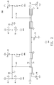
- FIG. 2 shows a schematic of one delay segment 200.
- the delay segment 200 may be any one of the delay elements 10-60 discussed above.
- Each of the delay segments include an identical schematic, although the various values of the components and lengths may be adjusted based on the desired delay time.
- the basic delay is provided by a coupled transmission line pair with, as an example, an even mode impedance of 129 ⁇ , an odd mode impedance of 31 ⁇ , and a uniform dielectric (thus, the same propagation speed for even and odd modes).
- any type of transmission line may be used and the disclosed embodiments are not limited to the example values.
- the example transmission line is commonly realizable on IC processes. For instance, two 4.0 ⁇ m tall, 4.2 ⁇ m wide lines with 3.5 ⁇ m spacing placed 12.4 ⁇ m above a ground plane in SiO 2 dielectric will approximate these impedances.
- One of the coupled lines, signal line 16, in each segment carries the signal to be delayed while the other line is switched selectively as part of the ground return path.
- the switches may be PIN diode switches.
- each end of the ground return path line 22 is switched to ground, placing ground return path line 22 in parallel with the common ground, lowering the net inductance of the signal line 16 in that segment.
- the signal travels the signal line 16 essentially at the speed of light.
- the ends of ground return path line 22 are not grounded, which forces the ground return current through the common ground, increasing the inductance of the signal line 16 in that segment.
- center of ground return path line 22 is switched to ground, so as to maintain the mutual capacitance of the lines, and extra capacitance is switched onto the signal line 16 to raise the segment capacitance by the same ratio as the inductance was raised. This increases the delay of the segment by that same ratio, while leaving the characteristic impedance unchanged.
- Segments of the lumped-element transmission line may be switched independently, so as to provide multiple steps in the overall delay, as discussed in more detail below. Segment lengths are set short enough to meet the desired delay resolution and to minimize the impact of reflections on the open-circuit ends of the ground return path line 22 in the segments switched for the long-delay mode.
- the signal to be delayed travels down signal line 16 of the coupled transmission line pair from node "in” to node "out.”
- DC control current 12 When DC control current 12 is sourced into control node "sell,” the current will flow through the second line to PIN diode switches 18 and 20, causing them to switch ON to a low impedance.
- This places ground return path line 22 in parallel with the common ground plane, lowering the impedance of line 16 to: Z 2 / 1 / Zeven + 1 / Zodd ⁇ 50 ⁇
- control node "selc" If control node "selc" is held below ground, reverse biasing PIN diode switches 24 and 26 to switch them OFF, the extra capacitors 28 and 32 are effectively removed from loading signal line 16, maintaining the desired 50 ⁇ impedance.
- the delay of the segment will equal the inherent delay of the coupled transmission lines, which is roughly 1ps for each 150 ⁇ m of length in SiO 2 or 4ps in this example. That is, in this example, the segment 200 is in the short-delay mode.
- Resistors 38, 42, 44, 46, 48, and 52 are present to insure diode switches 24 and 26 remain reverse-biased even in the presence of signal coupling through capacitors 28 and 32, but are chosen high enough in value to not represent a significant load on the AC signal coupled through the capacitors.
- resistors 38 and 46 may be 20k ⁇
- resistors 42 and 48 may be 14k ⁇
- resistors 44 and 52 may be 6k ⁇ .
- the delay ratio of a segment may reach 2:1 or more, much higher than would be acceptable for an impedance ratio in a capacitor-only tuning method.
- the PIN diode switches 24 and 26 in the disclosed technology are placed either in the ground return path 22 or in series with a capacitor. Thus, the switches 24 and 26 do not see and are not affected by the DC signal level, avoiding the delay change and non-linearity of the varactor approach discussed above.
- Segment length may be limited either by desired delay resolution or by keeping the segment delay well below the quarter wave length criteria for lumped element delay lines.
- the lumped element delay segments should be kept below a quarter wavelength of the desired operating frequency range. Only a few binary-weighted segments need to be limited by the desired delay resolution, but all segments need to be well below the quarter wave length criteria for lumped element delay lines. For example, as mentioned above, segments 50 and 60 are limited by the desired resolution, while the remaining segments 10-40 provide the maximum delay amount per segment, while being below a quarter wavelength of the desired operating frequency.
- the optimal sizing of PIN diode switches 18, 20, 24, 26, and 34 is generally a trade-off between ON resistance (favoring a large area to lower resistance) and OFF capacitance (favoring a small area to lower capacitance). Too much ON resistance in PIN diode switches 18 and 20 will add loss to the segment in the short-delay mode, whereas too much OFF capacitance will allow some high frequency current to flow out the ends of the lines, lowering the high frequency inductance and changing the delay in the long-delay mode.
- PIN diode switch 34 is unique in that it must be sized large to maintain a low ON resistance for low high frequency loss, but is rather insensitive to OFF capacitance as there is nominally no signal voltage present at that node in either delay mode.
- the dominant line loss is the combination of resistive loss in the signal line 16 and in the ground plane underneath.
- the parallel ground return path 22 through the coupled line serves to lower the ground loss, but ON resistance in the switches in the coupled line serves to raise ground loss.
- Proper sizing of the ground plane and switch resistance can match these effects, so loss is nominally the same in either delay mode.
- an alternate ground connection some distance away from the coupled line structure with a much lower resistance may be used if desired to minimize ground loss at low frequencies, in both delay modes, while still allowing matching of ground return loss at the higher frequencies where mutual inductance forces the ground return current into the ground plane underneath the coupled lines (and in the short-delay mode, into the grounded coupled line as well).
- Cextra may be added as a single capacitor 36 in the middle of the signal line 16.
- Examples provide an electronically variable analog delay line, comprising at least one segment with an electronically variable inductance, the at least one segment including a signal path, a ground return path, and one or more switches configured to vary the inductance of the segment.
- the at least one segment includes a short-delay mode and a long-delay mode, and the at least one segment is configured to delay a signal in the signal delay path a first delay amount in the short-delay mode and a second delay amount in the long-delay mode.
- the one or more switches includes three switches, two of the switches connected to ground at the ends of the ground return path, and the other of the switches connected to ground at the center of the ground return path.
- the two switches connected to ground at the ends of the ground return path are on, and the other of the switches is off
- the two switches connected to ground at the ends of the ground return path are off, and the other of the switches is on.
- the at least one segment further comprising at least one capacitor configured to add capacitance to the signal path during the long-delay mode.
- the capacitance added is the same ratio as the variance of inductance.
- the impedance of the electronically variable analog delay line is substantially unchanged between the short-delay mode and the long-delay mode.
- Some examples further comprise at least two segments with the electronically variable inductance.
- one segment of the at least two segments includes a different delay time in the short-delay mode and the long-delay mode than the other segment of the at least two segments.
- Some examples further comprise two switches to vary the inductance of the segment.
- Examples provide a method for delaying a signal on an electronically variable analog delay line, comprising switching between a short-delay mode and a long-delay mode, sending a signal on a signal path, adding capacitance to the signal path when in the long-delay mode to delay the signal by a first amount, and grounding a ground return path via turning on a first switch located at one end of the ground return path and a second switch located at the other end of the ground return path when in the short-delay mode to delay the signal by a second amount.
- Some examples further comprise varying the inductance of the electronically variable analog delay line between the short-delay mode and the long-delay mode.
- adding capacitance to the signal path when in the long-delay mode further includes turning on a center switch of the ground return path and turning off the first switch and the second switch of the ground return path.
- the impedance of the electronically variable analog delay line is substantially unchanged between the short-delay mode and the long-delay mode.
Landscapes
- Physics & Mathematics (AREA)
- Nonlinear Science (AREA)
- Ultra Sonic Daignosis Equipment (AREA)
- Networks Using Active Elements (AREA)
Abstract
Description
- This disclosure relates to an electronically variable analog delay line with a signal path and a ground return path to electronically vary the inductance of the electronically variable analog delay line in a short-delay mode and a long-delay mode.
- Differential input probes are commonly used to acquire a nominally differential signal, such as on a high-speed serial data bus, from a device under test (DUT) using a single test and measurement instrument channel. TriMode™ probes have the additional capability of acquiring the common-mode signal, or either side of the differential pair signal as a single-ended signal.
- An ideal differential signal includes two complementary signals sent on two separate wires. Any skew, or difference in delay, between the two sides of wiring in a DUT to the test and measurement instrument and/or within the test and measurement instrument itself causes mode conversion of the differential signal. Mode conversion is when a portion of the differential signal appears as the common-mode signal, or vice versa. Mode conversion due to skew grows progressively worse at higher frequencies. For instance, just one picosecond (ps) of skew at 25 GHz will lead to over 15% of the common-mode voltage appearing as a differential signal.
- One approach to minimizing errors due to the skew-related mode conversion is discussed in co-pending U.S. Application No.
14/745,757 - The electronically variable delays in U.S. Application No.
14/745,757 - Another known approach is to build a segmented delay line with microelectromechanical systems (MEMs) switches configured to switch in or out different segment lengths to implement a stepped delay control. This approach avoids the change in characteristic impedance with delay, but requires a specialized manufacturing process and may suffer significant insertion loss due to contact resistance of the MEMs switches.
- Yet another approach is the use of switched active delay elements (e.g., unity gain amplifiers that impart a relatively known delay to the signal). This approach is compatible with standard integrated chip (IC) processes, but degrades signal-to-noise ratio due to noise generation in the active stages, and may require more operational power than other approaches.
- Embodiments of the disclosed technology address these and other limitations in the prior art.
- Embodiments of the disclosed technology include an electronically variable analog delay line, including at least one segment with an electronically variable inductance. The at least one segment includes a signal path, a ground return path, and a plurality of switches configured to vary the inductance of the segment.
- Embodiments of the disclosed technology also include a method for delaying a signal on an electronically variable analog delay line. The method includes switching between a short-delay mode and a long-delay mode, sending a signal on a signal path, adding capacitance to the signal path when in the long-delay mode to delay the signal by a first amount, and grounding a ground return path via turning on a first switch located at one end of the ground return path and a second switch located at the other end of the ground return path when in the short-delay mode to delay the signal by a second amount.
-
-
Figure 1 shows an electronically variable analog delay line with multiple segments according to embodiments of the disclosed technology. -
Figure 2 illustrates a segment of the electronically variable analog delay line ofFigure 1 according to some embodiments of the disclosed technology. -
Figure 3 illustrates a segment of the electronically variable analog delay line ofFigure 1 according to other embodiments of the disclosed technology. - In the drawings, which are not necessarily to scale, like or corresponding elements of the disclosed systems and methods are denoted by the same reference numerals.
-
Figure 1 illustrates a lumped-element transmission line built using segments of coupled transmission lines, capacitors and switches, whileFigure 2 illustrates an example segment. -
Figure 1 shows a six-segment electronically variableanalog delay line 100 with fourequal delay segments additional segments segment 50 may be 0.5 the length of the four equal delay segments (resulting in a delay of nominally 2ps in the short-delay mode and 3.2ps in the long-delay mode) whilesegment 60 is 0.25 the length of the four equal delay segments (resulting in a delay nominally of lps in the short-delay mode and 1.6ps in the long-delay mode). This provides a net delay range of nominally 12ps and a delay resolution of nominally 0.6ps. The 6.4ps maximum delay per segment is below a quarter wavelength well past the desired 25 GHz operating frequency range of this example circuit. As discussed in more detail below, the maximum delay per segment must be below a quarter wavelength of the desired operating frequency. - Two
control currents Control current 12 controls the switches in the ground return path line 22 (shown inFigure 2 ) to adjust the effective line inductance, andcontrol current 14 controls the switches in series with the extra capacitors to adjust the effective line capacitance. In operation, bothcontrol currents - To create an adjustable delay, segments 10-60 may be switched in short-delay or long-delay mode to get the desired amount of time delay. Although six segments are shown in
Figure 1 , any number of segments may be used to reach the desired delay time and resolution. -
Figure 2 shows a schematic of onedelay segment 200. Thedelay segment 200 may be any one of the delay elements 10-60 discussed above. Each of the delay segments include an identical schematic, although the various values of the components and lengths may be adjusted based on the desired delay time. The basic delay is provided by a coupled transmission line pair with, as an example, an even mode impedance of 129Ω, an odd mode impedance of 31Ω, and a uniform dielectric (thus, the same propagation speed for even and odd modes). However, any type of transmission line may be used and the disclosed embodiments are not limited to the example values. The example transmission line is commonly realizable on IC processes. For instance, two 4.0µm tall, 4.2µm wide lines with 3.5µm spacing placed 12.4µm above a ground plane in SiO2 dielectric will approximate these impedances. - One of the coupled lines,
signal line 16, in each segment carries the signal to be delayed while the other line is switched selectively as part of the ground return path. In some embodiments, the switches may be PIN diode switches. In a short-delay mode, each end of the groundreturn path line 22 is switched to ground, placing groundreturn path line 22 in parallel with the common ground, lowering the net inductance of thesignal line 16 in that segment. In the short-delay mode, the signal travels thesignal line 16 essentially at the speed of light. In a long-delay mode, the ends of groundreturn path line 22 are not grounded, which forces the ground return current through the common ground, increasing the inductance of thesignal line 16 in that segment. Additionally, the center of groundreturn path line 22 is switched to ground, so as to maintain the mutual capacitance of the lines, and extra capacitance is switched onto thesignal line 16 to raise the segment capacitance by the same ratio as the inductance was raised. This increases the delay of the segment by that same ratio, while leaving the characteristic impedance unchanged. - Segments of the lumped-element transmission line may be switched independently, so as to provide multiple steps in the overall delay, as discussed in more detail below. Segment lengths are set short enough to meet the desired delay resolution and to minimize the impact of reflections on the open-circuit ends of the ground
return path line 22 in the segments switched for the long-delay mode. - The signal to be delayed travels down
signal line 16 of the coupled transmission line pair from node "in" to node "out." WhenDC control current 12 is sourced into control node "sell," the current will flow through the second line toPIN diode switches return path line 22 in parallel with the common ground plane, lowering the impedance ofline 16 to:
- If control node "selc" is held below ground, reverse biasing
PIN diode switches 24 and 26 to switch them OFF, theextra capacitors loading signal line 16, maintaining the desired 50Ω impedance. In this control state, the delay of the segment will equal the inherent delay of the coupled transmission lines, which is roughly 1ps for each 150µm of length in SiO2 or 4ps in this example. That is, in this example, thesegment 200 is in the short-delay mode. -
Resistors diode switches 24 and 26 remain reverse-biased even in the presence of signal coupling throughcapacitors resistors resistors resistors diode switches 24 and 26 to keep them from turning on. - However, to place the
segment 200 in the long-delay mode, the polarity of the control current 12 in control node "sell" is reversed so PIN diodes switches 18 and 20 will switch OFF andPIN diode switch 34 will switch ON instead. This continues to hold the groundreturn path line 22 at ground, maintaining the effect of mutual capacitance between the lines as capacitance to ground. Although three PIN diode switches 18, 20, and 34 are shown inFigure 2 , in alternative embodiments, one end of the groundreturn path line 22 could be permanently grounded while the other end of the groundreturn path line 22 is switched to ground or left open. The capacitance of thesignal line 16 remains:
- But, the signal's ground return current can no longer flow along the
line 22 with the ends open, so the impact of the mutual inductance between thelines signal line 16 impedance if the groundreturn path line 22 is floating is:
- Thus, the resulting
signal line 16 inductance without the groundreturn path line 22 as a ground return path is:
- DC control current 14 sourced into control node "selc" will flow into PIN diode switches 24 and 26, switching them ON and placing
capacitors signal line 16. This extra capacitance (that is, the sum ofcapacitors 28 and 32) may be set to:
- If Cextra is set as shown in equation (5), the lumped-element equivalent transmission line impedance for the segment will be the same as for the short-delay control state, but the delay will have increased by a ratio of:

- Tighter coupling of the lines will provide even higher delay ratios. For practical levels of line coupling in typical IC design processes, the delay ratio of a segment may reach 2:1 or more, much higher than would be acceptable for an impedance ratio in a capacitor-only tuning method. As seen in
Figure 2 , the PIN diode switches 24 and 26 in the disclosed technology are placed either in theground return path 22 or in series with a capacitor. Thus, theswitches 24 and 26 do not see and are not affected by the DC signal level, avoiding the delay change and non-linearity of the varactor approach discussed above. - Segment length may be limited either by desired delay resolution or by keeping the segment delay well below the quarter wave length criteria for lumped element delay lines. As mentioned above, the lumped element delay segments should be kept below a quarter wavelength of the desired operating frequency range. Only a few binary-weighted segments need to be limited by the desired delay resolution, but all segments need to be well below the quarter wave length criteria for lumped element delay lines. For example, as mentioned above,
segments - Higher line coupling provides for a higher delay ratio, and thus shorter total delay to achieve a target delay ranger. However, for a fixed target impedance (2/(1/Zeven+1/Zodd)), this requires a higher value of Zeven, which implies skinnier signal lines and more resistive loss in the conductor for a given delay. For any particular process and target impedance, there will be an optimal line coupling that minimizes loss by trading off between too long of a delay (at low coupling) versus too much loss per unit delay (at high coupling).
- The optimal sizing of PIN diode switches 18, 20, 24, 26, and 34 is generally a trade-off between ON resistance (favoring a large area to lower resistance) and OFF capacitance (favoring a small area to lower capacitance). Too much ON resistance in PIN diode switches 18 and 20 will add loss to the segment in the short-delay mode, whereas too much OFF capacitance will allow some high frequency current to flow out the ends of the lines, lowering the high frequency inductance and changing the delay in the long-delay mode.
- Likewise, too much ON resistance in PIN diode switches 24 and 26 will add high frequency loss to the segment in the long-delay mode, whereas too much OFF capacitance will impact the impedance and delay of the segment in the short-delay mode.
-
PIN diode switch 34 is unique in that it must be sized large to maintain a low ON resistance for low high frequency loss, but is rather insensitive to OFF capacitance as there is nominally no signal voltage present at that node in either delay mode. - In the long-delay mode, the dominant line loss is the combination of resistive loss in the
signal line 16 and in the ground plane underneath. In short-delay mode, the parallelground return path 22 through the coupled line serves to lower the ground loss, but ON resistance in the switches in the coupled line serves to raise ground loss. Proper sizing of the ground plane and switch resistance can match these effects, so loss is nominally the same in either delay mode. Although not shown, an alternate ground connection some distance away from the coupled line structure with a much lower resistance may be used if desired to minimize ground loss at low frequencies, in both delay modes, while still allowing matching of ground return loss at the higher frequencies where mutual inductance forces the ground return current into the ground plane underneath the coupled lines (and in the short-delay mode, into the grounded coupled line as well). - Other adjustments may be made based on circuit simulation and practical requirements. For instance, if some amount of impedance variation is acceptable, the effective delay range of a segment may be increased by selecting a higher value for Cextra than shown in equation (5). Also, although Cextra is shown as being added in two lumps at the one-quarter and three-quarter points along the segment lines, a different number and/or placement of the extra capacitance may be preferred, depending on the details of the layout and associated parasitics. For example, as seen in
Figure 3 , showing analternative segment 300, Cextra may be added as asingle capacitor 36 in the middle of thesignal line 16. - Examples provide an electronically variable analog delay line, comprising at least one segment with an electronically variable inductance, the at least one segment including a signal path, a ground return path, and one or more switches configured to vary the inductance of the segment.
- In some examples the at least one segment includes a short-delay mode and a long-delay mode, and the at least one segment is configured to delay a signal in the signal delay path a first delay amount in the short-delay mode and a second delay amount in the long-delay mode.
- In some examples the one or more switches includes three switches, two of the switches connected to ground at the ends of the ground return path, and the other of the switches connected to ground at the center of the ground return path.
- In some examples, during the short-delay mode, the two switches connected to ground at the ends of the ground return path are on, and the other of the switches is off, and during the long-delay mode, the two switches connected to ground at the ends of the ground return path are off, and the other of the switches is on.
- In some examples, the at least one segment further comprising at least one capacitor configured to add capacitance to the signal path during the long-delay mode.
- In some examples, the capacitance added is the same ratio as the variance of inductance.
- In some examples, the impedance of the electronically variable analog delay line is substantially unchanged between the short-delay mode and the long-delay mode.
- Some examples further comprise at least two segments with the electronically variable inductance.
- In some examples, one segment of the at least two segments includes a different delay time in the short-delay mode and the long-delay mode than the other segment of the at least two segments.
- Some examples further comprise two switches to vary the inductance of the segment.
- Examples provide a method for delaying a signal on an electronically variable analog delay line, comprising switching between a short-delay mode and a long-delay mode, sending a signal on a signal path, adding capacitance to the signal path when in the long-delay mode to delay the signal by a first amount, and grounding a ground return path via turning on a first switch located at one end of the ground return path and a second switch located at the other end of the ground return path when in the short-delay mode to delay the signal by a second amount.
- Some examples further comprise varying the inductance of the electronically variable analog delay line between the short-delay mode and the long-delay mode.
- In some examples, adding capacitance to the signal path when in the long-delay mode further includes turning on a center switch of the ground return path and turning off the first switch and the second switch of the ground return path.
- In some examples, the impedance of the electronically variable analog delay line is substantially unchanged between the short-delay mode and the long-delay mode.
- Having described and illustrated the principles of the disclosed technology in a preferred embodiment thereof, it should be apparent that the disclosed technology can be modified in arrangement and detail without departing from such principles. We claim all modifications and variations coming within the scope of the following claims.
Claims (14)
- An electronically variable analog delay line, comprising:at least one segment with an electronically variable inductance, the at least one segment including:a signal path;a ground return path; andone or more switches configured to vary the inductance of the segment.
- The electronically variable analog delay line of claim 1, wherein the at least one segment includes a short-delay mode and a long-delay mode, and the at least one segment is configured to delay a signal in the signal delay path a first delay amount in the short-delay mode and a second delay amount in the long-delay mode.
- The electronically variable analog delay line of claim 2, wherein the one or more switches includes three switches, two of the switches connected to ground at the ends of the ground return path, and the other of the switches connected to ground at the center of the ground return path.
- The electronically variable analog delay line of claim 3, wherein during the short-delay mode, the two switches connected to ground at the ends of the ground return path are on, and the other of the switches is off, and during the long-delay mode, the two switches connected to ground at the ends of the ground return path are off, and the other of the switches is on.
- The electronically variable analog delay line of claim 4, the at least one segment further comprising at least one capacitor configured to add capacitance to the signal path during the long-delay mode.
- The electronically variable analog delay line of claim 5, wherein the capacitance added is the same ratio as the variance of inductance.
- The electronically variable analog delay line of any of claims 2 to 6, wherein the impedance of the electronically variable analog delay line is substantially unchanged between the short-delay mode and the long-delay mode.
- The electronically variable analog delay line of any of claims 1 to 7, further comprising at least two segments with the electronically variable inductance.
- The electronically variable analog delay line of claim 8, wherein one segment of the at least two segments includes a different delay time in the short-delay mode and the long-delay mode than the other segment of the at least two segments.
- The electronically variable analog delay line of any of claims 1 to 9, further comprising two switches to vary the inductance of the segment.
- A method for delaying a signal on an electronically variable analog delay line, comprising:switching between a short-delay mode and a long-delay mode;sending a signal on a signal path;adding capacitance to the signal path when in the long-delay mode to delay the signal by a first amount; andgrounding a ground return path via turning on a first switch located at one end of the ground return path and a second switch located at the other end of the ground return path when in the short-delay mode to delay the signal by a second amount.
- The method of claim 11, further comprising varying the inductance of the electronically variable analog delay line between the short-delay mode and the long-delay mode.
- The method of claim 11 or 12, wherein adding capacitance to the signal path when in the long-delay mode further includes turning on a center switch of the ground return path and turning off the first switch and the second switch of the ground return path.
- The method of any of claims 11 to 13, wherein the impedance of the electronically variable analog delay line is substantially unchanged between the short-delay mode and the long-delay mode.
Applications Claiming Priority (1)
| Application Number | Priority Date | Filing Date | Title |
|---|---|---|---|
| US14/745,711 US9559663B2 (en) | 2015-06-22 | 2015-06-22 | Electronically variable analog delay line |
Publications (2)
| Publication Number | Publication Date |
|---|---|
| EP3110005A1 true EP3110005A1 (en) | 2016-12-28 |
| EP3110005B1 EP3110005B1 (en) | 2021-11-24 |
Family
ID=56235644
Family Applications (1)
| Application Number | Title | Priority Date | Filing Date |
|---|---|---|---|
| EP16175810.7A Active EP3110005B1 (en) | 2015-06-22 | 2016-06-22 | Electronically variable analog delay line |
Country Status (4)
| Country | Link |
|---|---|
| US (1) | US9559663B2 (en) |
| EP (1) | EP3110005B1 (en) |
| JP (1) | JP6928415B2 (en) |
| CN (1) | CN106257834B (en) |
Families Citing this family (1)
| Publication number | Priority date | Publication date | Assignee | Title |
|---|---|---|---|---|
| US12615040B2 (en) | 2023-10-06 | 2026-04-28 | Cornell University | Quasi true time delay |
Citations (3)
| Publication number | Priority date | Publication date | Assignee | Title |
|---|---|---|---|---|
| US4205282A (en) * | 1978-08-21 | 1980-05-27 | Westinghouse Electric Corp. | Phase shifting circuit element |
| FR2706098A1 (en) * | 1993-05-31 | 1994-12-09 | Mitsubishi Electric Corp | Several-bit phase shifter |
| US20140152399A1 (en) * | 2012-11-30 | 2014-06-05 | Qualcomm Incorporated | Digitally controlled phase shifter |
Family Cites Families (15)
| Publication number | Priority date | Publication date | Assignee | Title |
|---|---|---|---|---|
| US5180998A (en) * | 1991-11-05 | 1993-01-19 | Itt Corporation | Switched transmission line phase shifter apparatus employing multiple jets |
| CN2309028Y (en) * | 1997-08-10 | 1999-02-24 | 浙江阳光集团股份有限公司 | Electronic ballast with variable inductor |
| JP2004254155A (en) * | 2003-02-21 | 2004-09-09 | Kanji Otsuka | Signal transmission device and wiring structure |
| JP4221256B2 (en) * | 2003-07-31 | 2009-02-12 | 日本アンテナ株式会社 | Signal synthesizer |
| CN100530940C (en) * | 2007-08-14 | 2009-08-19 | 锐德科无线通信技术(上海)有限公司 | Gain fluctuation regulation circuit and method |
| US8193878B2 (en) * | 2008-06-24 | 2012-06-05 | International Business Machines Corporation | Structure, structure and method for providing an on-chip variable delay transmission line with fixed characteristic impedance |
| CN102027633B (en) * | 2008-06-24 | 2014-11-05 | 国际商业机器公司 | Design structure, structure and method for providing an on-chip variable delay transmission line with fixed characteristic impedance |
| US8344823B2 (en) * | 2009-08-10 | 2013-01-01 | Rf Controls, Llc | Antenna switching arrangement |
| US8503201B2 (en) * | 2009-12-03 | 2013-08-06 | Schneider Electric It Corporation | Transient clamping circuitry for voltage converter |
| US8898605B2 (en) * | 2010-10-25 | 2014-11-25 | International Business Machines Corporation | On-chip tunable transmission lines, methods of manufacture and design structures |
| CN102551779B (en) * | 2010-10-29 | 2015-02-18 | 株式会社东芝 | Variable delay device, device adjustment method and positron emission tomography system |
| WO2012168778A2 (en) * | 2011-06-07 | 2012-12-13 | Alcatel Lucent | A phase shifter for high power signal amplifying circuit and a method for shifting phase |
| US8988165B2 (en) * | 2012-01-27 | 2015-03-24 | Freescale Semiconductor, Inc | Delay line phase shifter with selectable phase shift |
| US9647722B2 (en) * | 2013-03-15 | 2017-05-09 | Dockon Ag | Adaptive line equalizer for improving data communication over less than perfect power lines or transmission lines |
| CN103491692B (en) * | 2013-10-14 | 2016-03-02 | 广东北江开关厂有限公司 | A kind of intelligent electric system for illumination |
-
2015
- 2015-06-22 US US14/745,711 patent/US9559663B2/en active Active
-
2016
- 2016-06-21 CN CN201610450872.7A patent/CN106257834B/en active Active
- 2016-06-22 JP JP2016123942A patent/JP6928415B2/en active Active
- 2016-06-22 EP EP16175810.7A patent/EP3110005B1/en active Active
Patent Citations (3)
| Publication number | Priority date | Publication date | Assignee | Title |
|---|---|---|---|---|
| US4205282A (en) * | 1978-08-21 | 1980-05-27 | Westinghouse Electric Corp. | Phase shifting circuit element |
| FR2706098A1 (en) * | 1993-05-31 | 1994-12-09 | Mitsubishi Electric Corp | Several-bit phase shifter |
| US20140152399A1 (en) * | 2012-11-30 | 2014-06-05 | Qualcomm Incorporated | Digitally controlled phase shifter |
Also Published As
| Publication number | Publication date |
|---|---|
| US9559663B2 (en) | 2017-01-31 |
| US20160373087A1 (en) | 2016-12-22 |
| EP3110005B1 (en) | 2021-11-24 |
| JP2017038357A (en) | 2017-02-16 |
| CN106257834B (en) | 2021-11-09 |
| JP6928415B2 (en) | 2021-09-01 |
| CN106257834A (en) | 2016-12-28 |
Similar Documents
| Publication | Publication Date | Title |
|---|---|---|
| US6784679B2 (en) | Differential coaxial contact array for high-density, high-speed signals | |
| JP4616861B2 (en) | Signal transmission circuit and signal transmission system | |
| EP1605588B1 (en) | Wide bandwidth attenuator input circuit for a measurement probe | |
| US7907033B2 (en) | Tunable impedance matching networks and tunable diplexer matching systems | |
| US7170365B2 (en) | Ultrafast sampler with non-parallel shockline | |
| US20010024116A1 (en) | Electronic probe for measuring high impedance tri-state logic circuits | |
| US20090278624A1 (en) | Reflection-type phase shifter having reflection loads implemented using transmission lines and phased-array receiver/transmitter utilizing the same | |
| US20070207746A1 (en) | Apparatus for controlling impedance | |
| CN1173054A (en) | Balun transformer | |
| US6098176A (en) | Sinusoidal clock signal distribution using resonant transmission lines | |
| WO2008135597A1 (en) | Electrical component with a front-end circuit | |
| US7855614B2 (en) | Integrated circuit transmission lines, methods for designing integrated circuits using the same and methods to improve return loss | |
| EP3110005B1 (en) | Electronically variable analog delay line | |
| CN103185823B (en) | A kind of oscillograph with compensating for frequency response circuit | |
| CN112350671B (en) | Electronic circuit and method for providing adjustable signal delay duration | |
| JP2006191355A (en) | equalizer | |
| US8274340B2 (en) | Parallel transmission lines having different path lengths and including different properties for equalizing the path lengths there between | |
| US20250148180A1 (en) | Negative Group Delay Filters based on Reciprocal-capped Butterworth, Reciprocal-capped Chebyshev, and Reciprocal-capped Bessel low-pass Filter Transfer Functions | |
| US20130099797A1 (en) | Variable Impedance Device | |
| KR100674742B1 (en) | High frequency switch circuit device | |
| KR101513464B1 (en) | Apparatus for wideband variable true-time delay | |
| EP1908187A1 (en) | Antenna array | |
| JP2005101946A (en) | Power distribution synthesizer | |
| WO1999035740A1 (en) | Artificial line | |
| US20250379365A1 (en) | Phase shifting apparatus and process |
Legal Events
| Date | Code | Title | Description |
|---|---|---|---|
| PUAI | Public reference made under article 153(3) epc to a published international application that has entered the european phase |
Free format text: ORIGINAL CODE: 0009012 |
|
| STAA | Information on the status of an ep patent application or granted ep patent |
Free format text: STATUS: THE APPLICATION HAS BEEN PUBLISHED |
|
| AK | Designated contracting states |
Kind code of ref document: A1 Designated state(s): AL AT BE BG CH CY CZ DE DK EE ES FI FR GB GR HR HU IE IS IT LI LT LU LV MC MK MT NL NO PL PT RO RS SE SI SK SM TR |
|
| AX | Request for extension of the european patent |
Extension state: BA ME |
|
| STAA | Information on the status of an ep patent application or granted ep patent |
Free format text: STATUS: REQUEST FOR EXAMINATION WAS MADE |
|
| 17P | Request for examination filed |
Effective date: 20170628 |
|
| RBV | Designated contracting states (corrected) |
Designated state(s): AL AT BE BG CH CY CZ DE DK EE ES FI FR GB GR HR HU IE IS IT LI LT LU LV MC MK MT NL NO PL PT RO RS SE SI SK SM TR |
|
| STAA | Information on the status of an ep patent application or granted ep patent |
Free format text: STATUS: EXAMINATION IS IN PROGRESS |
|
| 17Q | First examination report despatched |
Effective date: 20180213 |
|
| GRAP | Despatch of communication of intention to grant a patent |
Free format text: ORIGINAL CODE: EPIDOSNIGR1 |
|
| STAA | Information on the status of an ep patent application or granted ep patent |
Free format text: STATUS: GRANT OF PATENT IS INTENDED |
|
| RIC1 | Information provided on ipc code assigned before grant |
Ipc: H03K 5/00 20060101ALN20210331BHEP Ipc: H03K 5/133 20140101ALI20210331BHEP Ipc: H01P 9/00 20060101ALI20210331BHEP Ipc: H03H 7/34 20060101ALI20210331BHEP Ipc: H03H 7/18 20060101AFI20210331BHEP |
|
| INTG | Intention to grant announced |
Effective date: 20210421 |
|
| GRAJ | Information related to disapproval of communication of intention to grant by the applicant or resumption of examination proceedings by the epo deleted |
Free format text: ORIGINAL CODE: EPIDOSDIGR1 |
|
| STAA | Information on the status of an ep patent application or granted ep patent |
Free format text: STATUS: EXAMINATION IS IN PROGRESS |
|
| GRAP | Despatch of communication of intention to grant a patent |
Free format text: ORIGINAL CODE: EPIDOSNIGR1 |
|
| STAA | Information on the status of an ep patent application or granted ep patent |
Free format text: STATUS: GRANT OF PATENT IS INTENDED |
|
| INTC | Intention to grant announced (deleted) | ||
| GRAS | Grant fee paid |
Free format text: ORIGINAL CODE: EPIDOSNIGR3 |
|
| RIC1 | Information provided on ipc code assigned before grant |
Ipc: H03K 5/00 20060101ALN20210915BHEP Ipc: H03K 5/133 20140101ALI20210915BHEP Ipc: H01P 9/00 20060101ALI20210915BHEP Ipc: H03H 7/34 20060101ALI20210915BHEP Ipc: H03H 7/18 20060101AFI20210915BHEP |
|
| GRAA | (expected) grant |
Free format text: ORIGINAL CODE: 0009210 |
|
| STAA | Information on the status of an ep patent application or granted ep patent |
Free format text: STATUS: THE PATENT HAS BEEN GRANTED |
|
| INTG | Intention to grant announced |
Effective date: 20210930 |
|
| AK | Designated contracting states |
Kind code of ref document: B1 Designated state(s): AL AT BE BG CH CY CZ DE DK EE ES FI FR GB GR HR HU IE IS IT LI LT LU LV MC MK MT NL NO PL PT RO RS SE SI SK SM TR |
|
| REG | Reference to a national code |
Ref country code: GB Ref legal event code: FG4D |
|
| REG | Reference to a national code |
Ref country code: DE Ref legal event code: R096 Ref document number: 602016066510 Country of ref document: DE |
|
| REG | Reference to a national code |
Ref country code: AT Ref legal event code: REF Ref document number: 1450643 Country of ref document: AT Kind code of ref document: T Effective date: 20211215 |
|
| REG | Reference to a national code |
Ref country code: IE Ref legal event code: FG4D |
|
| REG | Reference to a national code |
Ref country code: LT Ref legal event code: MG9D |
|
| REG | Reference to a national code |
Ref country code: NL Ref legal event code: MP Effective date: 20211124 |
|
| REG | Reference to a national code |
Ref country code: AT Ref legal event code: MK05 Ref document number: 1450643 Country of ref document: AT Kind code of ref document: T Effective date: 20211124 |
|
| PG25 | Lapsed in a contracting state [announced via postgrant information from national office to epo] |
Ref country code: RS Free format text: LAPSE BECAUSE OF FAILURE TO SUBMIT A TRANSLATION OF THE DESCRIPTION OR TO PAY THE FEE WITHIN THE PRESCRIBED TIME-LIMIT Effective date: 20211124 Ref country code: LT Free format text: LAPSE BECAUSE OF FAILURE TO SUBMIT A TRANSLATION OF THE DESCRIPTION OR TO PAY THE FEE WITHIN THE PRESCRIBED TIME-LIMIT Effective date: 20211124 Ref country code: FI Free format text: LAPSE BECAUSE OF FAILURE TO SUBMIT A TRANSLATION OF THE DESCRIPTION OR TO PAY THE FEE WITHIN THE PRESCRIBED TIME-LIMIT Effective date: 20211124 Ref country code: BG Free format text: LAPSE BECAUSE OF FAILURE TO SUBMIT A TRANSLATION OF THE DESCRIPTION OR TO PAY THE FEE WITHIN THE PRESCRIBED TIME-LIMIT Effective date: 20220224 Ref country code: AT Free format text: LAPSE BECAUSE OF FAILURE TO SUBMIT A TRANSLATION OF THE DESCRIPTION OR TO PAY THE FEE WITHIN THE PRESCRIBED TIME-LIMIT Effective date: 20211124 |
|
| PG25 | Lapsed in a contracting state [announced via postgrant information from national office to epo] |
Ref country code: IS Free format text: LAPSE BECAUSE OF FAILURE TO SUBMIT A TRANSLATION OF THE DESCRIPTION OR TO PAY THE FEE WITHIN THE PRESCRIBED TIME-LIMIT Effective date: 20220324 Ref country code: SE Free format text: LAPSE BECAUSE OF FAILURE TO SUBMIT A TRANSLATION OF THE DESCRIPTION OR TO PAY THE FEE WITHIN THE PRESCRIBED TIME-LIMIT Effective date: 20211124 Ref country code: PT Free format text: LAPSE BECAUSE OF FAILURE TO SUBMIT A TRANSLATION OF THE DESCRIPTION OR TO PAY THE FEE WITHIN THE PRESCRIBED TIME-LIMIT Effective date: 20220324 Ref country code: PL Free format text: LAPSE BECAUSE OF FAILURE TO SUBMIT A TRANSLATION OF THE DESCRIPTION OR TO PAY THE FEE WITHIN THE PRESCRIBED TIME-LIMIT Effective date: 20211124 Ref country code: NO Free format text: LAPSE BECAUSE OF FAILURE TO SUBMIT A TRANSLATION OF THE DESCRIPTION OR TO PAY THE FEE WITHIN THE PRESCRIBED TIME-LIMIT Effective date: 20220224 Ref country code: NL Free format text: LAPSE BECAUSE OF FAILURE TO SUBMIT A TRANSLATION OF THE DESCRIPTION OR TO PAY THE FEE WITHIN THE PRESCRIBED TIME-LIMIT Effective date: 20211124 Ref country code: LV Free format text: LAPSE BECAUSE OF FAILURE TO SUBMIT A TRANSLATION OF THE DESCRIPTION OR TO PAY THE FEE WITHIN THE PRESCRIBED TIME-LIMIT Effective date: 20211124 Ref country code: HR Free format text: LAPSE BECAUSE OF FAILURE TO SUBMIT A TRANSLATION OF THE DESCRIPTION OR TO PAY THE FEE WITHIN THE PRESCRIBED TIME-LIMIT Effective date: 20211124 Ref country code: GR Free format text: LAPSE BECAUSE OF FAILURE TO SUBMIT A TRANSLATION OF THE DESCRIPTION OR TO PAY THE FEE WITHIN THE PRESCRIBED TIME-LIMIT Effective date: 20220225 Ref country code: ES Free format text: LAPSE BECAUSE OF FAILURE TO SUBMIT A TRANSLATION OF THE DESCRIPTION OR TO PAY THE FEE WITHIN THE PRESCRIBED TIME-LIMIT Effective date: 20211124 |
|
| PG25 | Lapsed in a contracting state [announced via postgrant information from national office to epo] |
Ref country code: SM Free format text: LAPSE BECAUSE OF FAILURE TO SUBMIT A TRANSLATION OF THE DESCRIPTION OR TO PAY THE FEE WITHIN THE PRESCRIBED TIME-LIMIT Effective date: 20211124 Ref country code: SK Free format text: LAPSE BECAUSE OF FAILURE TO SUBMIT A TRANSLATION OF THE DESCRIPTION OR TO PAY THE FEE WITHIN THE PRESCRIBED TIME-LIMIT Effective date: 20211124 Ref country code: RO Free format text: LAPSE BECAUSE OF FAILURE TO SUBMIT A TRANSLATION OF THE DESCRIPTION OR TO PAY THE FEE WITHIN THE PRESCRIBED TIME-LIMIT Effective date: 20211124 Ref country code: EE Free format text: LAPSE BECAUSE OF FAILURE TO SUBMIT A TRANSLATION OF THE DESCRIPTION OR TO PAY THE FEE WITHIN THE PRESCRIBED TIME-LIMIT Effective date: 20211124 Ref country code: DK Free format text: LAPSE BECAUSE OF FAILURE TO SUBMIT A TRANSLATION OF THE DESCRIPTION OR TO PAY THE FEE WITHIN THE PRESCRIBED TIME-LIMIT Effective date: 20211124 Ref country code: CZ Free format text: LAPSE BECAUSE OF FAILURE TO SUBMIT A TRANSLATION OF THE DESCRIPTION OR TO PAY THE FEE WITHIN THE PRESCRIBED TIME-LIMIT Effective date: 20211124 |
|
| REG | Reference to a national code |
Ref country code: DE Ref legal event code: R097 Ref document number: 602016066510 Country of ref document: DE |
|
| PLBE | No opposition filed within time limit |
Free format text: ORIGINAL CODE: 0009261 |
|
| STAA | Information on the status of an ep patent application or granted ep patent |
Free format text: STATUS: NO OPPOSITION FILED WITHIN TIME LIMIT |
|
| PG25 | Lapsed in a contracting state [announced via postgrant information from national office to epo] |
Ref country code: AL Free format text: LAPSE BECAUSE OF FAILURE TO SUBMIT A TRANSLATION OF THE DESCRIPTION OR TO PAY THE FEE WITHIN THE PRESCRIBED TIME-LIMIT Effective date: 20211124 |
|
| 26N | No opposition filed |
Effective date: 20220825 |
|
| PG25 | Lapsed in a contracting state [announced via postgrant information from national office to epo] |
Ref country code: SI Free format text: LAPSE BECAUSE OF FAILURE TO SUBMIT A TRANSLATION OF THE DESCRIPTION OR TO PAY THE FEE WITHIN THE PRESCRIBED TIME-LIMIT Effective date: 20211124 |
|
| PG25 | Lapsed in a contracting state [announced via postgrant information from national office to epo] |
Ref country code: MC Free format text: LAPSE BECAUSE OF FAILURE TO SUBMIT A TRANSLATION OF THE DESCRIPTION OR TO PAY THE FEE WITHIN THE PRESCRIBED TIME-LIMIT Effective date: 20211124 |
|
| REG | Reference to a national code |
Ref country code: CH Ref legal event code: PL |
|
| REG | Reference to a national code |
Ref country code: BE Ref legal event code: MM Effective date: 20220630 |
|
| GBPC | Gb: european patent ceased through non-payment of renewal fee |
Effective date: 20220622 |
|
| PG25 | Lapsed in a contracting state [announced via postgrant information from national office to epo] |
Ref country code: LU Free format text: LAPSE BECAUSE OF NON-PAYMENT OF DUE FEES Effective date: 20220622 Ref country code: LI Free format text: LAPSE BECAUSE OF NON-PAYMENT OF DUE FEES Effective date: 20220630 Ref country code: IE Free format text: LAPSE BECAUSE OF NON-PAYMENT OF DUE FEES Effective date: 20220622 Ref country code: FR Free format text: LAPSE BECAUSE OF NON-PAYMENT OF DUE FEES Effective date: 20220630 Ref country code: CH Free format text: LAPSE BECAUSE OF NON-PAYMENT OF DUE FEES Effective date: 20220630 |
|
| PG25 | Lapsed in a contracting state [announced via postgrant information from national office to epo] |
Ref country code: IT Free format text: LAPSE BECAUSE OF FAILURE TO SUBMIT A TRANSLATION OF THE DESCRIPTION OR TO PAY THE FEE WITHIN THE PRESCRIBED TIME-LIMIT Effective date: 20211124 Ref country code: GB Free format text: LAPSE BECAUSE OF NON-PAYMENT OF DUE FEES Effective date: 20220622 Ref country code: BE Free format text: LAPSE BECAUSE OF NON-PAYMENT OF DUE FEES Effective date: 20220630 |
|
| P01 | Opt-out of the competence of the unified patent court (upc) registered |
Effective date: 20230530 |
|
| PG25 | Lapsed in a contracting state [announced via postgrant information from national office to epo] |
Ref country code: HU Free format text: LAPSE BECAUSE OF FAILURE TO SUBMIT A TRANSLATION OF THE DESCRIPTION OR TO PAY THE FEE WITHIN THE PRESCRIBED TIME-LIMIT; INVALID AB INITIO Effective date: 20160622 |
|
| PG25 | Lapsed in a contracting state [announced via postgrant information from national office to epo] |
Ref country code: MK Free format text: LAPSE BECAUSE OF FAILURE TO SUBMIT A TRANSLATION OF THE DESCRIPTION OR TO PAY THE FEE WITHIN THE PRESCRIBED TIME-LIMIT Effective date: 20211124 Ref country code: CY Free format text: LAPSE BECAUSE OF FAILURE TO SUBMIT A TRANSLATION OF THE DESCRIPTION OR TO PAY THE FEE WITHIN THE PRESCRIBED TIME-LIMIT Effective date: 20211124 |
|
| PG25 | Lapsed in a contracting state [announced via postgrant information from national office to epo] |
Ref country code: MT Free format text: LAPSE BECAUSE OF FAILURE TO SUBMIT A TRANSLATION OF THE DESCRIPTION OR TO PAY THE FEE WITHIN THE PRESCRIBED TIME-LIMIT Effective date: 20211124 |
|
| PG25 | Lapsed in a contracting state [announced via postgrant information from national office to epo] |
Ref country code: TR Free format text: LAPSE BECAUSE OF FAILURE TO SUBMIT A TRANSLATION OF THE DESCRIPTION OR TO PAY THE FEE WITHIN THE PRESCRIBED TIME-LIMIT Effective date: 20211124 |
|
| PGFP | Annual fee paid to national office [announced via postgrant information from national office to epo] |
Ref country code: DE Payment date: 20260629 Year of fee payment: 11 |