EP3109575B1 - Apparatus and method for cryocooled devices thermalization with rf electrical signals - Google Patents
Apparatus and method for cryocooled devices thermalization with rf electrical signals Download PDFInfo
- Publication number
- EP3109575B1 EP3109575B1 EP15173469.6A EP15173469A EP3109575B1 EP 3109575 B1 EP3109575 B1 EP 3109575B1 EP 15173469 A EP15173469 A EP 15173469A EP 3109575 B1 EP3109575 B1 EP 3109575B1
- Authority
- EP
- European Patent Office
- Prior art keywords
- thermalization
- plate
- wire
- chamber
- ims
- Prior art date
- Legal status (The legal status is an assumption and is not a legal conclusion. Google has not performed a legal analysis and makes no representation as to the accuracy of the status listed.)
- Active
Links
Images


Classifications
-
- F—MECHANICAL ENGINEERING; LIGHTING; HEATING; WEAPONS; BLASTING
- F17—STORING OR DISTRIBUTING GASES OR LIQUIDS
- F17C—VESSELS FOR CONTAINING OR STORING COMPRESSED, LIQUEFIED OR SOLIDIFIED GASES; FIXED-CAPACITY GAS-HOLDERS; FILLING VESSELS WITH, OR DISCHARGING FROM VESSELS, COMPRESSED, LIQUEFIED, OR SOLIDIFIED GASES
- F17C13/00—Details of vessels or of the filling or discharging of vessels
-
- F—MECHANICAL ENGINEERING; LIGHTING; HEATING; WEAPONS; BLASTING
- F25—REFRIGERATION OR COOLING; COMBINED HEATING AND REFRIGERATION SYSTEMS; HEAT PUMP SYSTEMS; MANUFACTURE OR STORAGE OF ICE; LIQUEFACTION SOLIDIFICATION OF GASES
- F25D—REFRIGERATORS; COLD ROOMS; ICE-BOXES; COOLING OR FREEZING APPARATUS NOT OTHERWISE PROVIDED FOR
- F25D19/00—Arrangement or mounting of refrigeration units with respect to devices or objects to be refrigerated, e.g. infrared detectors
- F25D19/006—Thermal coupling structure or interface
-
- G—PHYSICS
- G01—MEASURING; TESTING
- G01J—MEASUREMENT OF INTENSITY, VELOCITY, SPECTRAL CONTENT, POLARISATION, PHASE OR PULSE CHARACTERISTICS OF INFRARED, VISIBLE OR ULTRAVIOLET LIGHT; COLORIMETRY; RADIATION PYROMETRY
- G01J1/00—Photometry, e.g. photographic exposure meter
- G01J1/02—Details
- G01J1/0252—Constructional arrangements for compensating for fluctuations caused by, e.g. temperature, or using cooling or temperature stabilization of parts of the device; Controlling the atmosphere inside a photometer; Purge systems, cleaning devices
-
- G—PHYSICS
- G01—MEASURING; TESTING
- G01J—MEASUREMENT OF INTENSITY, VELOCITY, SPECTRAL CONTENT, POLARISATION, PHASE OR PULSE CHARACTERISTICS OF INFRARED, VISIBLE OR ULTRAVIOLET LIGHT; COLORIMETRY; RADIATION PYROMETRY
- G01J5/00—Radiation pyrometry, e.g. infrared or optical thermometry
- G01J5/02—Constructional details
- G01J5/06—Arrangements for eliminating effects of disturbing radiation; Arrangements for compensating changes in sensitivity
- G01J5/061—Arrangements for eliminating effects of disturbing radiation; Arrangements for compensating changes in sensitivity by controlling the temperature of the apparatus or parts thereof, e.g. using cooling means or thermostats
-
- F—MECHANICAL ENGINEERING; LIGHTING; HEATING; WEAPONS; BLASTING
- F17—STORING OR DISTRIBUTING GASES OR LIQUIDS
- F17C—VESSELS FOR CONTAINING OR STORING COMPRESSED, LIQUEFIED OR SOLIDIFIED GASES; FIXED-CAPACITY GAS-HOLDERS; FILLING VESSELS WITH, OR DISCHARGING FROM VESSELS, COMPRESSED, LIQUEFIED, OR SOLIDIFIED GASES
- F17C2203/00—Vessel construction, in particular walls or details thereof
-
- F—MECHANICAL ENGINEERING; LIGHTING; HEATING; WEAPONS; BLASTING
- F17—STORING OR DISTRIBUTING GASES OR LIQUIDS
- F17C—VESSELS FOR CONTAINING OR STORING COMPRESSED, LIQUEFIED OR SOLIDIFIED GASES; FIXED-CAPACITY GAS-HOLDERS; FILLING VESSELS WITH, OR DISCHARGING FROM VESSELS, COMPRESSED, LIQUEFIED, OR SOLIDIFIED GASES
- F17C2205/00—Vessel construction, in particular mounting arrangements, attachments or identifications means
-
- F—MECHANICAL ENGINEERING; LIGHTING; HEATING; WEAPONS; BLASTING
- F25—REFRIGERATION OR COOLING; COMBINED HEATING AND REFRIGERATION SYSTEMS; HEAT PUMP SYSTEMS; MANUFACTURE OR STORAGE OF ICE; LIQUEFACTION SOLIDIFICATION OF GASES
- F25D—REFRIGERATORS; COLD ROOMS; ICE-BOXES; COOLING OR FREEZING APPARATUS NOT OTHERWISE PROVIDED FOR
- F25D2400/00—General features of, or devices for refrigerators, cold rooms, ice-boxes, or for cooling or freezing apparatus not covered by any other subclass
- F25D2400/28—Quick cooling
-
- F—MECHANICAL ENGINEERING; LIGHTING; HEATING; WEAPONS; BLASTING
- F25—REFRIGERATION OR COOLING; COMBINED HEATING AND REFRIGERATION SYSTEMS; HEAT PUMP SYSTEMS; MANUFACTURE OR STORAGE OF ICE; LIQUEFACTION SOLIDIFICATION OF GASES
- F25D—REFRIGERATORS; COLD ROOMS; ICE-BOXES; COOLING OR FREEZING APPARATUS NOT OTHERWISE PROVIDED FOR
- F25D2400/00—General features of, or devices for refrigerators, cold rooms, ice-boxes, or for cooling or freezing apparatus not covered by any other subclass
- F25D2400/30—Quick freezing
-
- F—MECHANICAL ENGINEERING; LIGHTING; HEATING; WEAPONS; BLASTING
- F25—REFRIGERATION OR COOLING; COMBINED HEATING AND REFRIGERATION SYSTEMS; HEAT PUMP SYSTEMS; MANUFACTURE OR STORAGE OF ICE; LIQUEFACTION SOLIDIFICATION OF GASES
- F25D—REFRIGERATORS; COLD ROOMS; ICE-BOXES; COOLING OR FREEZING APPARATUS NOT OTHERWISE PROVIDED FOR
- F25D2400/00—General features of, or devices for refrigerators, cold rooms, ice-boxes, or for cooling or freezing apparatus not covered by any other subclass
- F25D2400/40—Refrigerating devices characterised by electrical wiring
-
- G—PHYSICS
- G01—MEASURING; TESTING
- G01J—MEASUREMENT OF INTENSITY, VELOCITY, SPECTRAL CONTENT, POLARISATION, PHASE OR PULSE CHARACTERISTICS OF INFRARED, VISIBLE OR ULTRAVIOLET LIGHT; COLORIMETRY; RADIATION PYROMETRY
- G01J1/00—Photometry, e.g. photographic exposure meter
- G01J1/42—Photometry, e.g. photographic exposure meter using electric radiation detectors
- G01J1/44—Electric circuits
- G01J2001/4413—Type
- G01J2001/442—Single-photon detection or photon counting
Definitions
- the present invention relates generally to the field of RF (Radio Frequency) signals and cryocooled devices, and more specifically to high performance thermalization of cryocooled devices with high bandwidth RF electrical connectionss.
- RF Radio Frequency
- cryocooling system One of the well known issues concerning devices working at cryogenic temperatures is the minimal temperature that a cryocooling system is able to reach for a given thermal power dissipation.
- a user who wants to work below a given temperature value, needs to be sure that the system's thermal power dissipation under cooling is below a corresponding threshold value of power dissipation.
- a threshold value depends on the thermal connection between the cryocooling system and device under cooling.
- the first well known strategy in order to reduce as much as possible the thermal power dissipation of a device is to put it into a vacuum chamber.
- the power dissipation is limited by the thermal radiation of the device.
- the system power dissipation increases due to the wire thermal conduction.
- a conductive element such as a wire
- all the heat propagating through the wire will increase the system (and therefore device) temperature. This temperature increase might affect the device performance if the system behavior is strongly temperature dependent as is for example the case of devices made of superconducting material.
- cryostat working systems One way of reducing the thermal power dissipation of a cryocooled device due to thermal conduction of a physical connection is usually described as "Thermalization" in cryostat working systems.
- Thermalization is a process of reducing the temperature of conductive elements, used for the connection between a cryocooled device and its surrounding vacuum chamber, to reduce as much as possible the temperature difference between those elements and the cryocooled system at the connection point.
- One way to implement thermalization is to thermally connect the conductive elements to a mechanical piece which is at a low intermediate temperature, so that the heat, propagating through these elements, is pulled out at that point, rather than travelling onto the device or sample to be measured up to the cryocooled system.
- the physical connections that can be done between a cryocooled system and the outside of the vacuum chamber are used for the propagation of physical signals such as electrical or optical signals. Those physical connections can be made of metal, glass or plastic depending on the type of signals that propagates through them.
- the challenge may therefore be generally described as having a good electrical conductivity while maintaining a good dissipation property at cryogenic temperature (for example 3K); more precisely the challenge is to maintain an RF line with minimal attenuation and minimal heat load to the sample.
- thermalization process consists in lowering the heat flow Q and according to the previous simplified model; three (3) main solutions families can be distinguished:
- Alternatively Sapphire may be used as a substrate for thermal dissipation
- US 2015/0060190 discloses such type of solution where a Sapphire-PC board having high heat conductivity at low temperature is used to reduce noise and temperature during measurement.
- Niobium Nitride Single photon optical detector NbN-based SSPD or SNSPD
- a chip carrier which ensures a good thermal contact during optical measurement.
- it is composed of a connector, a small printed PCB and a Copper (Cu) plate.
- This embodiment has been specifically used to fasten measurement characterization while reducing the probability of damaging a SSPD.
- Attenuation solutions are used. (Slichter & al., 2009) describe two set-ups using specific stripline designed to have significant attenuation at 1.3GHz and 1.5GHz. These specific realizations used in the mK temperature range show that the dynamic range of the measurement decreases with frequency due to the attenuation in the cryogenic coaxial lines. These proposed filters are therefore effective at suppressing high frequency electromagnetic noise without radiating non-equilibrium thermal noise; present a well-matched 50 ⁇ impedance, thus well suited for measurements involving quantum devices.
- Non-patent literature includes:
- the general idea of the invention is to connect the sample located in the cryostat chamber to be measured through wires to a specific plate enabling wire line thermalization between cryostat chambers.
- an Insulated Metal Substrate (IMS) layer somehow similar to those used for heat dissipation in high temperature environment (e.g.: for power device or LED applications) has been adapted for cryostat functioning.
- electrical and thermal measurement shows IMS applicability for cryogenic temperatures, whereas it is generally specified for thermal cycling in the range of 230K - 520K.
- the IMS board used for wire line thermalization in cryostat environment may embed active devices for several functionalities such as processing or signal amplification.
- a first aspect of the invention therefore relates to a cryogenic device comprising at least two chambers at two different temperatures, a first chamber at a first temperature T1 accommodating a sample, and a second chamber at a second temperature T2 greater than T1 and being adapted to accommodate a cooling device, said cooling device being adapted to cool wirelines connecting said sample to an external element, wherein said cooling device is a thermalization plate comprising at least one wire-guide having an input for plugging a wire line connected to the sample and an output for plugging a wire line connected to said external element, said wire-guide being thermally connected to the first chamber, characterized in that said thermalization plate is an Insulated Metal Substrate (IMS) plate. Therefore, it is possible to redirect and dissipate the heat flow to the walls instead of the first chamber.
- IMS Insulated Metal Substrate
- the thermalization plate is mounted on a mechanical attachment made of a thermally conductive material and thermally connected to the first chamber.
- the thermalization plate embeds an active device for signal amplification or processing.
- the wirelines are coaxial cables.
- the thermalization plate is located in the second chamber.
- the thermalization plate comprises at least a first layer comprising a material with high thermal conductivity in thermal contact with the first chamber; a second layer made of a thin dielectric material as an insulating layer; and a third layer is made of conductive material used for forming the circuitry enabling wire thermalization.
- the thermalization plate is adapted to fit a defined impedance.
- wire length, material and depth on thermalization plate may be adapted to get 50 ⁇ or 75 ⁇ circuits.
- the chambers are electrically connected to each other through feeding through-holes provided in the walls of the chambers.
- a second aspect of the invention is a process for installing an IMS thermalization board inside a cryogenic device of the first aspect of the invention comprising the steps of:
- thermalization plate made with IMS technology which combines the properties presented above. It is of particular interest, that IMS has never been specified at cryogenic temperatures, and the inventors surprisingly found that such a plate made with this technology was compatible with the thermal (high heat dissipation) and electrical requirements (impedance matching and high bandwidth) of the present device.
- Fig. 1a shows a cryostat 100 is made of three chambers 110, 120 and 130 at three different temperatures T3, T2 and T1 with preferably, T3 > T2 > T1.
- T3 may be in the order of magnitude of few hundred Kelvin (typically 200K), T2 at the order of 20K and T1 at the level of 2K .
- Each chamber is connected electrically to the other through feeding through-holes 030 provided in the walls of the chamber.
- These three chambers 110, 120, 130 enable to have a smooth temperature transition from T3 (typically in the range of 200K) in the third chamber 110 to T1 (typically in the range of 2K) in the first chamber 130 comprising an analyzed sample 131 by using cold finger 010 filed with He that is provided second chamber 120.
- Fig. 1b is an enlarged view of chambers 120 and 130.
- sample 131 is connected to the higher temperature chamber 120 through wires 160 used for data acquisition.
- a first wire 160 is connected from the sample 131 to a thermalization plate 170.
- a second wire 150 is connecting the thermalizing plate 170 to the external environment.
- the apparatus used for thermalization 170 is mechanically and thermally connected to the cryostat last chamber baseline 020 at T1 thanks to a mechanical attachment 140. Being thermally coupled to the first chamber 130, the mechanical attachment 140 acts like a thermal drain. This thermal drain ensures thermal dissipation and temperature transition from T2 to T1.
- the general idea of the invention is to connect the sample 131 located in the chamber 130 at cryogenic temperature T1 to a thermalization plate 170 with at least one wire 160. Further preferably, the thermalization plate 170 is connected to the external environment through a wire that may be a coaxial cable 150
- Fig. 2a shows a preferred embodiment of the thermalization plate 170.
- This thermalization plate is an IMS plate and is preferably composed of N wirelines connected to N inputs 105 ports and N output ports 106 connected by wires of length L 108.
- Thermalization plate input temperature is at T1 and output temperature is at T2.
- This plate is adapted with 50 ⁇ impedance so that so that high-frequency (above 1GHz) and weak signals may be transmitted without any attenuation.
- any suitable cable type may be used between the sample 131 and thermalization plate 170, whereas the output thermalization plate 170 may consist in cables adapted to avoid thermal dissipation such as coaxial cables.
- wire length L 108 is adapted in order to ensure a gradient from T1 which is the temperature of the first cryostat chamber (at the level of 2K) at the input to T2 which is the temperature of the second cryostat chamber (at the level of 20K) at the output. Therefore, with this thermalization plate 170 one can, from the electrical point of view, adapt wirelines with high bandwidth signals which means, low attenuation at high frequencies and it is possible to design easily wirelines in order to adapt their impedance to the input/output impedance. Finally, from a thermal point of view the thermalization plate ensures that all parts of the coaxial cable, namely the shield and conductive core, are thermally anchored at the required temperature of T1, avoiding excessive heating of the sample.
- the first thermalization plate 170 described is composed of inactive components, namely wires used to transmit electrical signals.
- the thermalization plate may embed active device for signal amplification or processing. This can have several advantages among them, the proximity to the signal source leading to lower interference pickup, lower noise or increase system bandwidth.
- Fig. 2b shows the thermalization plate 170 structure based on IMS technology used within a cryostat and used for wirelines thermalization. It has been mechanically adapted as described below for working in cryostat conditions.
- the IMS plate is composed of at least five (5) layers each of them in charge of a specific function.
- First layer 206 is dedicated to heat dissipation through conduction phenomenon, and consists in a layer made with a material with high thermal conductivity. As an example it may be Al or Cu. This heat dissipation layer helps to spread thermal energy at the lower bound of the thermalization plate.
- Second layer 205 is an insulator layer made of a thin dielectric layer enabling to separate and discriminate electrically conductive layers from heat dissipation layer.
- Third layer 204 is made of conductive material used for forming the circuitry enabling wire thermalization.
- two additional layers 203, and 202 are preferably used for thermal and electrical insulation which are namely the solder mask and solder paste.
- wirelines realized on IMS board enables to thermalize wirelines from temperature T1 to temperature T2 and spread thermal power through thermal drain
- Fig 3 depicts the IMS thermalization board, ready to be installed inside a cryostat.
- the following method may be used.
- the first step 301 consists in putting the IMS plate 170 in contact with a part of cryostat at T1.
- the thermalization plate 170 may be placed outside the T1 chamber at cryogenic temperature 130. It is outside the T1 cryogenic chamber, and then the thermalization plate 170 may be fixed to a mechanical attachment 140 (optionally made of metal or the like) acting in this case as a thermal drain which can be considered as an additional step 301' of the present method.
- the second step 302 consists in connecting the cable 150 coming from the outside of the chamber 120 at temperature T2 on one of the output connectors of the plate 106.
- the third step 303 consists in connecting the corresponding cable 160 coming from the chamber 130 at temperature T1 to the connector 105 on the plate linked to the previously cited connector through the wire-guide. Note that it is important that two cables that have to be linked together are connected to the same wire-guide.
- Fig 4 shows, as previously described, that the disclosed invention relies on the exploitation of IMS board technology for cryostat and wire line thermalization.
- two graphs are presented based on the characterization of an SNSPD detector without a thermalization plate (a) and with a thermalization plate (b).
- thermalization plate allow proper functioning of the SNSPD detector List of Reference Signs (100) - Cryostat (170) Thermalization plate (010) - Cryostat cold finger (206) Thermalization plate first layer - heat spreader (020) - T1 cryostat chamber baseline (030) - Feed through hole (205) Second layer - insulating layer (120) - 2 nd Cryostat chamber (at T2) (204) third layer - conducting wires (105) thermalization plate input (203) Fourth layer - solder mask (106) thermalization plate output (202) Fifth layer - solder paste (108) L thermalization plate wire length (301) - First method step (110) - 3 rd cryostat chamber (At T3) (302) - Second method step (130) - 1 st Cryostat chamber (
Landscapes
- Engineering & Computer Science (AREA)
- Physics & Mathematics (AREA)
- General Physics & Mathematics (AREA)
- Spectroscopy & Molecular Physics (AREA)
- Mechanical Engineering (AREA)
- General Engineering & Computer Science (AREA)
- Chemical & Material Sciences (AREA)
- Combustion & Propulsion (AREA)
- Thermal Sciences (AREA)
- Electromagnetism (AREA)
- Containers, Films, And Cooling For Superconductive Devices (AREA)
Description
- The present invention relates generally to the field of RF (Radio Frequency) signals and cryocooled devices, and more specifically to high performance thermalization of cryocooled devices with high bandwidth RF electrical connexions.
- One of the well known issues concerning devices working at cryogenic temperatures is the minimal temperature that a cryocooling system is able to reach for a given thermal power dissipation. For a given cryocooling system, a user, who wants to work below a given temperature value, needs to be sure that the system's thermal power dissipation under cooling is below a corresponding threshold value of power dissipation. Such a threshold value depends on the thermal connection between the cryocooling system and device under cooling.
- The first well known strategy in order to reduce as much as possible the thermal power dissipation of a device is to put it into a vacuum chamber. In this case, the power dissipation is limited by the thermal radiation of the device. However, when the device needs to be connected to any external system through a physical connection (e.g. a wire), the system power dissipation increases due to the wire thermal conduction. As an example, if a conductive element (such as a wire), is thermally connected directly from room temperature to a cryocooled system temperature all the heat propagating through the wire will increase the system (and therefore device) temperature. This temperature increase might affect the device performance if the system behavior is strongly temperature dependent as is for example the case of devices made of superconducting material.
- One way of reducing the thermal power dissipation of a cryocooled device due to thermal conduction of a physical connection is usually described as "Thermalization" in cryostat working systems.
- Thermalization is a process of reducing the temperature of conductive elements, used for the connection between a cryocooled device and its surrounding vacuum chamber, to reduce as much as possible the temperature difference between those elements and the cryocooled system at the connection point. One way to implement thermalization is to thermally connect the conductive elements to a mechanical piece which is at a low intermediate temperature, so that the heat, propagating through these elements, is pulled out at that point, rather than travelling onto the device or sample to be measured up to the cryocooled system. For example, if a wire is sufficiently thermally connected to a 30K temperature part of a cryostat, then most of the heat coming from the wire end at room temperature and propagating through this wire will be absorbed by the cryostat part and much less heat will propagate from the 30K temperature cryostat part to the cryocooled device or sample. As a consequence, this may impact and lower the sample performances which should be obtained under cryogenic conditions and moreover damage the structure to be measured or characterized. In general, the physical connections that can be done between a cryocooled system and the outside of the vacuum chamber are used for the propagation of physical signals such as electrical or optical signals. Those physical connections can be made of metal, glass or plastic depending on the type of signals that propagates through them. The challenge may therefore be generally described as having a good electrical conductivity while maintaining a good dissipation property at cryogenic temperature (for example 3K); more precisely the challenge is to maintain an RF line with minimal attenuation and minimal heat load to the sample.
- A well known approach to model heat and thermal flow by conduction is described by the following simplified formula:
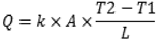
- "Q" is the heat flow in Watts
- "k" is the conductivity of the material and usually measured in W/ (m*K)
- "A" is the cross-sectional area of the wire (m2)
- "L" is the length of the wire (m)
- "T2-T1" is the temperature gradient across the wire
- Several approaches have been proposed for cryostat thermalization process. Based on the simplified model, thermalization process consists in lowering the heat flow Q and according to the previous simplified model; three (3) main solutions families can be distinguished:
- The 1st one is dealing with solutions lowering wire cross-sectional area (A) or wire material thermal conductive (k) by using for instance coaxial cables. Such type of cables are described as an example in
US 7.446.257 disclosing the use of a dielectric and insulating material surrounding the center conductor enables to define a cable with appropriate thermal and electrical properties to be used in a cryostat. Such coaxial cables for low temperature consist of low thermal conductivity metal materials on center and outer conductors, material of center and conductor may be chosen between Cupronickel, Stainless Steel, Niobium, Beryllium copper, Brass or other materials. - The 2nd one is dealing with solutions increasing L. Increasing wire length enables to increase the wire heat surface exchange within the cryostat, which enables to get appropriate dissipation property. Such solution can consist in circling cables around cold finger.
- (Gorla et al., 2003) provide a thermalization solution disclosed for 1.2K and 1K working temperature. Proposed solution relies on a capillary tube in the line between the main bath and 1K plots that is thermalized on a copper screw at 1K temperature.
- These two solutions are based on the optimization of 'A' and/or 'L' which is acceptable for wires made of glass or plastic where optical signal propagate, because this optimization doesn't reduce the propagation performances of the optical signal. On the other hand, for metallic wires, the electrical resistivity of these wires increases when their cross section decreases and their length increases. Hence, the optimization of those parameters for reducing the heat flow impacts the electrical properties of those wires. This is the reason why for metallic wires, it is the thermal conductivity which is most of all optimized (i.e. reduced).
- Whereas the first two families are dealing with solutions dedicated to wire characteristics, the last one is dealing with solutions related to the wire environment and consists in using several means to dissipate thermal heat depending on the operating temperature range from few hundred Kelvin to mK.
- More particularly and especially in the case of detecting weak signal infrared radiation, attempts are made to overcome noise that originates from unwanted IR flux that is out of the visible light and which is reflected on the internal components of the cryostat
US 8.664.606 discloses an apparatus working at temperatures from 50 to 200K. - Alternatively Sapphire may be used as a substrate for thermal dissipation,
US 2015/0060190 discloses such type of solution where a Sapphire-PC board having high heat conductivity at low temperature is used to reduce noise and temperature during measurement. - Document
EP1063482 discloses all the technical features from the preamble of the independent claim 1 of the present invention. - (Casaburi & al., 2007) in the context of Niobium Nitride Single photon optical detector (NbN-based SSPD or SNSPD) describe the use of a chip carrier which ensures a good thermal contact during optical measurement. In this case, it is composed of a connector, a small printed PCB and a Copper (Cu) plate. This embodiment has been specifically used to fasten measurement characterization while reducing the probability of damaging a SSPD.
- Additionally, in order to perform measurements of thermal and electrical characteristics, attenuation solutions are used. (Slichter & al., 2009) describe two set-ups using specific stripline designed to have significant attenuation at 1.3GHz and 1.5GHz. These specific realizations used in the mK temperature range show that the dynamic range of the measurement decreases with frequency due to the attenuation in the cryogenic coaxial lines. These proposed filters are therefore effective at suppressing high frequency electromagnetic noise without radiating non-equilibrium thermal noise; present a well-matched 50Ω impedance, thus well suited for measurements involving quantum devices.
- Non-patent literature includes:
- Casaburi A., Ejrnaes M, Quaranta O, Gaggero A, Mattioli F., Leoni R., Voronov B., Lisitskiy M., Esposito E., Nappi C., Cristiano R., Pagano S., Experimental characterization of NbN nanowire optical detectors with parallel stripline configuration, 2008, Journal of Physics Conference Series; 97(1):012265. DOI: 10.1088/1742-6596/97/1/012265
- Gorla P., Bucci C., Pirro S., Complete elimination of 1K Pot vibrations in dilution refrigerators, 2003, Nuclear Instruments and Methods in Physics Research A 520, 641-643.
- Slichter D.H., Naaman O., Siddiqi I., Millikelvin thermal and electrical performance of lossy transmission line filters, 2009, Applied Physics Letters, 94(19): 192508 - 192508-3
- Therefore existing solutions are complex to industrialize for cryostat application and to put in a production process. Moreover at high frequencies, circuits often require coaxial cables and connectors. The same issues of length, materials and lagging apply plus additional issues such as heat losses through the core and bandwidth. One of the main issues with coaxial cables is that while one can lag outer shield, it is difficult to pull the heat out of the inner core. This is because the insulating dielectric materials used between the shield and the core typically have low thermal conductivity. Moreover, although a huge variety of commercial heat spreader are used for electrical signal conditions near room temperature (in the range of 200 - 400K), none of these are specified for cryogenic temperatures (in the range of 0 - 150K).
- Based on this prior art it is an object of the present invention to provide to cryostat users the possibility to thermalize wire lines in order to detect weak signals coming from sample measurement. This issue is particularly critical when dealing with RF signals and cryocooled devices, and more specifically high performance thermalization of cryocooled devices with high bandwidth RF electrical connections. Moreover, high frequency circuits often require coaxial cables and connectors. The same issues of length, materials and lagging apply plus additional issues such as heat loss through the core and bandwidth. Therefore it is valuable to have a simple and customizable solution enabling wireline thermalization between a cryostat chamber at low temperature and the sample to be measured which is located in a chamber at cryogenic temperature.
- The general idea of the invention is to connect the sample located in the cryostat chamber to be measured through wires to a specific plate enabling wire line thermalization between cryostat chambers. In order to achieve thermalization wire lines, an Insulated Metal Substrate (IMS) layer somehow similar to those used for heat dissipation in high temperature environment (e.g.: for power device or LED applications) has been adapted for cryostat functioning. Interestingly enough, electrical and thermal measurement shows IMS applicability for cryogenic temperatures, whereas it is generally specified for thermal cycling in the range of 230K - 520K.
- In order to achieve this, one need to be able to include an IMS plate within a cryostat while enabling wireline thermalization during its operation. This invention is solving this issue by disclosing an apparatus and the associated method. Alternatively, the IMS board used for wire line thermalization in cryostat environment may embed active devices for several functionalities such as processing or signal amplification.
- A first aspect of the invention therefore relates to a cryogenic device comprising at least two chambers at two different temperatures, a first chamber at a first temperature T1 accommodating a sample, and a second chamber at a second temperature T2 greater than T1 and being adapted to accommodate a cooling device, said cooling device being adapted to cool wirelines connecting said sample to an external element, wherein said cooling device is a thermalization plate comprising at least one wire-guide having an input for plugging a wire line connected to the sample and an output for plugging a wire line connected to said external element, said wire-guide being thermally connected to the first chamber, characterized in that said thermalization plate is an Insulated Metal Substrate (IMS) plate. Therefore, it is possible to redirect and dissipate the heat flow to the walls instead of the first chamber.
- Advantageously, the thermalization plate is mounted on a mechanical attachment made of a thermally conductive material and thermally connected to the first chamber.
- Still advantageously, the thermalization plate embeds an active device for signal amplification or processing.
- Still advantageously, the wirelines are coaxial cables.
- Still advantageously, the thermalization plate is located in the second chamber.
- Still advantageously, the thermalization plate comprises at least a first layer comprising a material with high thermal conductivity in thermal contact with the first chamber; a second layer made of a thin dielectric material as an insulating layer; and a third layer is made of conductive material used for forming the circuitry enabling wire thermalization.
- Still advantageously, the thermalization plate is adapted to fit a defined impedance. As an example wire length, material and depth on thermalization plate may be adapted to get 50Ω or 75Ω circuits.
- Still advantageously, the chambers are electrically connected to each other through feeding through-holes provided in the walls of the chambers.
- A second aspect of the invention is a process for installing an IMS thermalization board inside a cryogenic device of the first aspect of the invention comprising the steps of:
- putting the IMS plate in contact with a part of cryostat at T1;
- connecting the output cable on one of the output connectors of the Insulated Metal Substrate (IMS) thermalization board;
- connecting the input cable to the input connector on the same wire-guide of the Insulated Metal Substrate (IMS) thermalization board as the output cable.
- There are multiple benefits associated to this invention as it is adapted for industrialization and mass production, adapted to weak and high-frequency signal transmission and experiments and measurements confirm the particular suitability of this solution in the case of SNSPD or SSPD (Superconducting Nanowire Single-Photon Detector) cases. Further embodiments of the invention are laid down in the dependent claims.
- Preferred embodiments of the invention are described in the following with reference to the drawings, which are for the purpose of illustrating the present preferred embodiments of the invention and not for the purpose of limiting the same. In the drawings,
-
Fig. 1a - is a schematic view of a cryostat apparatus of the invention; -
Fig. 1b - is an enlarged schematic view of a cooling system included in the cryostat offigure 1a ; -
Fig. 2a - is an upper view of the thermalization plate with and without active devices; -
Fig. 2b - is a cross-section view of the thermalization plate offigure 2a ; -
Fig. 3 - is a picture and diagram of the method associated to the apparatus embodiment; -
Fig. 4a - is a graph presenting measurement results without the thermalization plate. -
Fig. 4b - is a graph presenting measurements results with a thermalization plate. - The invention description is based on the attached
figures 1a to 4b . - With this invention, we describe a thermalization plate made with IMS technology which combines the properties presented above. It is of particular interest, that IMS has never been specified at cryogenic temperatures, and the inventors surprisingly found that such a plate made with this technology was compatible with the thermal (high heat dissipation) and electrical requirements (impedance matching and high bandwidth) of the present device.
-
Fig. 1a shows acryostat 100 is made of threechambers holes 030 provided in the walls of the chamber. These threechambers third chamber 110 to T1 (typically in the range of 2K) in thefirst chamber 130 comprising an analyzedsample 131 by usingcold finger 010 filed with He that is providedsecond chamber 120. -
Fig. 1b is an enlarged view ofchambers sample 131 to be measured in thefirst chamber 130 in cryogenic conditions, that is at temperature T1 and that is attached to thecold finger 010 and thermally and mechanically anchored using appropriate screws in order to be cooled to cryogenic temperature. In order to acquire sample signals,sample 131 is connected to thehigher temperature chamber 120 throughwires 160 used for data acquisition. Afirst wire 160 is connected from thesample 131 to athermalization plate 170. Asecond wire 150 is connecting thethermalizing plate 170 to the external environment. Preferably, the apparatus used forthermalization 170 is mechanically and thermally connected to the cryostatlast chamber baseline 020 at T1 thanks to amechanical attachment 140. Being thermally coupled to thefirst chamber 130, themechanical attachment 140 acts like a thermal drain. This thermal drain ensures thermal dissipation and temperature transition from T2 to T1. - Therefore, the general idea of the invention is to connect the
sample 131 located in thechamber 130 at cryogenic temperature T1 to athermalization plate 170 with at least onewire 160. Further preferably, thethermalization plate 170 is connected to the external environment through a wire that may be acoaxial cable 150 -
Fig. 2a shows a preferred embodiment of thethermalization plate 170. This thermalization plate is an IMS plate and is preferably composed of N wirelines connected toN inputs 105 ports andN output ports 106 connected by wires oflength L 108. Thermalization plate input temperature is at T1 and output temperature is at T2. This plate is adapted with 50Ω impedance so that so that high-frequency (above 1GHz) and weak signals may be transmitted without any attenuation. By doing so, one of the main advantages is that any suitable cable type may be used between thesample 131 andthermalization plate 170, whereas theoutput thermalization plate 170 may consist in cables adapted to avoid thermal dissipation such as coaxial cables. With this embodiment,wire length L 108 is adapted in order to ensure a gradient from T1 which is the temperature of the first cryostat chamber (at the level of 2K) at the input to T2 which is the temperature of the second cryostat chamber (at the level of 20K) at the output. Therefore, with thisthermalization plate 170 one can, from the electrical point of view, adapt wirelines with high bandwidth signals which means, low attenuation at high frequencies and it is possible to design easily wirelines in order to adapt their impedance to the input/output impedance. Finally, from a thermal point of view the thermalization plate ensures that all parts of the coaxial cable, namely the shield and conductive core, are thermally anchored at the required temperature of T1, avoiding excessive heating of the sample. - The
first thermalization plate 170 described is composed of inactive components, namely wires used to transmit electrical signals. Alternatively, the thermalization plate may embed active device for signal amplification or processing. This can have several advantages among them, the proximity to the signal source leading to lower interference pickup, lower noise or increase system bandwidth. -
Fig. 2b shows thethermalization plate 170 structure based on IMS technology used within a cryostat and used for wirelines thermalization. It has been mechanically adapted as described below for working in cryostat conditions. The IMS plate is composed of at least five (5) layers each of them in charge of a specific function. -
First layer 206 is dedicated to heat dissipation through conduction phenomenon, and consists in a layer made with a material with high thermal conductivity. As an example it may be Al or Cu. This heat dissipation layer helps to spread thermal energy at the lower bound of the thermalization plate. -
Second layer 205 is an insulator layer made of a thin dielectric layer enabling to separate and discriminate electrically conductive layers from heat dissipation layer. -
Third layer 204 is made of conductive material used for forming the circuitry enabling wire thermalization. - Above these conductive tracks, two
additional layers - Therefore, wirelines realized on IMS board enables to thermalize wirelines from temperature T1 to temperature T2 and spread thermal power through thermal drain
-
Fig 3 depicts the IMS thermalization board, ready to be installed inside a cryostat. In order to get this IMS thermalization board within a cryostat, the following method may be used. - The
first step 301 consists in putting theIMS plate 170 in contact with a part of cryostat at T1. Thethermalization plate 170 may be placed outside the T1 chamber atcryogenic temperature 130. It is outside the T1 cryogenic chamber, and then thethermalization plate 170 may be fixed to a mechanical attachment 140 (optionally made of metal or the like) acting in this case as a thermal drain which can be considered as an additional step 301' of the present method. - The
second step 302 consists in connecting thecable 150 coming from the outside of thechamber 120 at temperature T2 on one of the output connectors of theplate 106. - The
third step 303 consists in connecting thecorresponding cable 160 coming from thechamber 130 at temperature T1 to theconnector 105 on the plate linked to the previously cited connector through the wire-guide. Note that it is important that two cables that have to be linked together are connected to the same wire-guide. -
Fig 4 shows, as previously described, that the disclosed invention relies on the exploitation of IMS board technology for cryostat and wire line thermalization. In this figure two graphs are presented based on the characterization of an SNSPD detector without a thermalization plate (a) and with a thermalization plate (b). - These two graphs plot the Detection Efficiency as a function of the bias current in (µA). Experiment without thermalization plate shows that typical saturation plateau can not be obtained above 5.5 µA. In the opposite, with thermalization plate, a
detection plateau 401 is obtained from 5.0 µA to 6.2 µA corresponding to the maximum detection efficiency. Thisdetection plateau 401 is clearly one of the characteristics of the single-photon detection regime corresponding to weak signal detection. Moreover, thisdetection plateau 401 corresponds to the regime where the internal quantum efficiency of the single photon detector is near 100%. Clearly this regime is sought after in applications using SNSPDs since higher detection efficiency typically means better performance. The fact that the saturation plateau without the thermalization plate is smaller, shows that the SNSPD device is being heated by heat flow through the center core of the coaxial cable, which is badly thermalized, hence reducing the performance of the SNSPD. In that specific case, the thermalization plate allow proper functioning of the SNSPD detectorList of Reference Signs (100) - Cryostat (170) Thermalization plate (010) - Cryostat cold finger (206) Thermalization plate first layer - heat spreader (020) - T1 cryostat chamber baseline (030) - Feed through hole (205) Second layer - insulating layer (120) - 2nd Cryostat chamber (at T2) (204) third layer - conducting wires (105) thermalization plate input (203) Fourth layer - solder mask (106) thermalization plate output (202) Fifth layer - solder paste (108) L thermalization plate wire length (301) - First method step (110) - 3rd cryostat chamber (At T3) (302) - Second method step (130) - 1st Cryostat chamber (at T1) (303) - Third method step (131) - Device / Sample (401) - Detection Efficiency Plateau (140) - Mechanical attachment / Thermal drain (150) Outside cable (160) wires used for data acquisition
Claims (8)
- Cryogenic device comprising at least two chambers (120, 130) at two different temperatures, a first chamber (130) at a first temperature T1 accommodating a sample (131), and a second chamber (120) at a second temperature T2 greater than T1 and being adapted to accommodate a cooling device (170), said cooling device (170) being adapted to cool wirelines (150, 160) connecting said sample (131) to an external element, wherein said cooling device (170) is a thermalization plate (170) comprising at least one wire-guide having an input (105) for plugging a wire line (160) connected to the sample and an output (106) for plugging a wire line (150) connected to said external element, said wire-guide being thermally connected to the first chamber (130), characterized in that said thermalization plate (170) is an Insulated Metal Substrate (IMS) plate (170).
- Cryogenic device according to claim 1, wherein said thermalization plate (170) is mounted on a mechanical attachment (140) made of a thermally conductive material and thermally connected to the first chamber (130).
- Cryogenic device according to any one of claims 1 to 2, wherein the thermalization plate (170) embeds an active device (201) for signal amplification or processing.
- Cryogenic device according to any one of claims 1 to 3, wherein the wirelines (150, 160) are coaxial cables.
- Cryogenic device according to any one of claims 1 to 4, wherein the thermalization plate (170) comprises
a first layer (206) comprising a material with high thermal conductivity;
a second layer (205) made of a thin dielectric material as an insulating layer;
a third layer (204) is made of conductive material used for forming the circuitry enabling wire thermalization; and
two layers (203, 202) which are a solder mask and a solder paste. - Cryogenic device according to any one of claims 1 to 5, wherein the thermalization plate (170) is adapted to fit a specific impedance value.
- Cryogenic device according to any one of claims 1 to 5, wherein the chambers (120, 130) are electrically connected to each other through feeding through-holes (030) provided in the walls of the chambers (120, 130).
- Process for installing an Insulated Metal Substrate (IMS) thermalization board (170) inside the cryogenic device of any of claims 1-7 comprising the steps of:- putting the Insulated Metal Substrate (IMS) plate (170) in contact with a part of the cryogenic device at T1;- connecting the output cable (150) on one of the output connectors (106) of the Insulated Metal Substrate (IMS) thermalization board (170);- connecting the input cable (160) to the input connector (105) on the same wire-guide of the Insulated Metal Substrate (IMS) thermalization board (170) as the output cable (150).
Priority Applications (2)
| Application Number | Priority Date | Filing Date | Title |
|---|---|---|---|
| EP15173469.6A EP3109575B1 (en) | 2015-06-23 | 2015-06-23 | Apparatus and method for cryocooled devices thermalization with rf electrical signals |
| US15/189,426 US10145513B2 (en) | 2015-06-23 | 2016-06-22 | Apparatus and method for cryocooled devices thermalization with RF electrical signals |
Applications Claiming Priority (1)
| Application Number | Priority Date | Filing Date | Title |
|---|---|---|---|
| EP15173469.6A EP3109575B1 (en) | 2015-06-23 | 2015-06-23 | Apparatus and method for cryocooled devices thermalization with rf electrical signals |
Publications (2)
| Publication Number | Publication Date |
|---|---|
| EP3109575A1 EP3109575A1 (en) | 2016-12-28 |
| EP3109575B1 true EP3109575B1 (en) | 2018-10-10 |
Family
ID=53502453
Family Applications (1)
| Application Number | Title | Priority Date | Filing Date |
|---|---|---|---|
| EP15173469.6A Active EP3109575B1 (en) | 2015-06-23 | 2015-06-23 | Apparatus and method for cryocooled devices thermalization with rf electrical signals |
Country Status (2)
| Country | Link |
|---|---|
| US (1) | US10145513B2 (en) |
| EP (1) | EP3109575B1 (en) |
Families Citing this family (10)
| Publication number | Priority date | Publication date | Assignee | Title |
|---|---|---|---|---|
| DE102017130755A1 (en) | 2017-12-20 | 2019-06-27 | Bilfinger Noell Gmbh | Apparatus for analyzing an atmosphere and use of the apparatus |
| CN108362389B (en) * | 2018-02-02 | 2019-12-10 | 中国科学院上海微系统与信息技术研究所 | Method and system for improving counting rate of superconducting nanowire single photon detector |
| US10601096B2 (en) | 2018-02-12 | 2020-03-24 | International Business Machines Corporation | Reduced thermal resistance attenuator on high-thermal conductivity substrates for quantum applications |
| US10505245B2 (en) | 2018-02-12 | 2019-12-10 | International Business Machines Corporation | Microwave attenuators on high-thermal conductivity substrates for quantum applications |
| US10621503B1 (en) | 2018-12-03 | 2020-04-14 | International Business Machines Corporation | Quantum computer hardware with reflectionless filters for thermalizing radio frequency signals |
| US11079281B2 (en) * | 2019-01-17 | 2021-08-03 | Uvia Group Llc | Cold stage actuation of optical elements including an optical light shield and a lenslet array connected to a cold finger |
| US11620559B2 (en) | 2019-02-06 | 2023-04-04 | International Business Machines Corporation | Reduction of spontaneous emission and thermal photon noise in quantum computing machines using a galvanically grounded filter |
| US11499764B2 (en) * | 2019-09-04 | 2022-11-15 | Quantinuum Llc | Cable management for cryogenic system |
| US11788685B2 (en) * | 2021-01-08 | 2023-10-17 | International Business Machines Corporation | 1 kelvin and 300 millikelvin thermal stages for cryogenic environments |
| GB2616318B (en) | 2022-05-16 | 2024-05-15 | Oxford Instruments Nanotechnology Tools Ltd | Cryogenic cooling system |
Family Cites Families (8)
| Publication number | Priority date | Publication date | Assignee | Title |
|---|---|---|---|---|
| AU5685000A (en) * | 1999-06-24 | 2001-01-31 | Csp Cryogenic Spectrometers Gmbh | Cooling device |
| EP1063482A1 (en) * | 1999-06-24 | 2000-12-27 | CSP Cryogenic Spectrometers GmbH | Refrigeration device |
| US7446257B2 (en) | 2006-01-11 | 2008-11-04 | Andrew Llc | Coaxial cable with fine wire inner conductor and method of manufacture |
| US8464542B2 (en) * | 2007-12-28 | 2013-06-18 | D-Wave Systems Inc. | Systems, methods, and apparatus for cryogenic refrigeration |
| FR2968398B1 (en) | 2010-12-02 | 2014-04-11 | Soc Fr Detecteurs Infrarouges Sofradir | INFRARED RADIATION DETECTOR |
| WO2012168225A1 (en) * | 2011-06-06 | 2012-12-13 | Centre National De La Recherche Scientifique - Cnrs - | Ion source, nanofabrication apparatus comprising such source, and a method for emitting ions |
| US20140137571A1 (en) * | 2012-11-21 | 2014-05-22 | D-Wave Systems Inc. | Systems and methods for cryogenic refrigeration |
| US9826622B2 (en) | 2013-08-27 | 2017-11-21 | President And Fellows Of Harvard College | Reducing noise and temperature during measurements in cryostats |
-
2015
- 2015-06-23 EP EP15173469.6A patent/EP3109575B1/en active Active
-
2016
- 2016-06-22 US US15/189,426 patent/US10145513B2/en active Active
Non-Patent Citations (1)
| Title |
|---|
| None * |
Also Published As
| Publication number | Publication date |
|---|---|
| US20160377230A1 (en) | 2016-12-29 |
| EP3109575A1 (en) | 2016-12-28 |
| US10145513B2 (en) | 2018-12-04 |
Similar Documents
| Publication | Publication Date | Title |
|---|---|---|
| US10145513B2 (en) | Apparatus and method for cryocooled devices thermalization with RF electrical signals | |
| US20230067066A1 (en) | Connecting Electrical Circuitry in a Quantum Computing System | |
| KR102606554B1 (en) | Reduce losses in superconducting cables | |
| US7012419B2 (en) | Fast Faraday cup with high bandwidth | |
| TW507216B (en) | Signal transmission cable with a noise absorbing high loss magnetic film formed on a sheath of the cable | |
| JPS6359274B2 (en) | ||
| JP6008356B2 (en) | Microwave connector, connector and method of assembling the connector | |
| WO2025077543A1 (en) | Heat shielding device and josephson junction array chip system | |
| Thalmann et al. | Comparison of cryogenic low-pass filters | |
| JP2014041104A (en) | Probe for magnetic resonance signal detection | |
| Colless et al. | Cryogenic high-frequency readout and control platform for spin qubits | |
| JP7119079B2 (en) | Thermally insulated ground plane with superconducting electrical coupler | |
| JP2005214792A (en) | Superconducting X-ray detector and superconducting X-ray analyzer using the same | |
| Ramarao et al. | Development of 3 kW at 325 MHz solid-state RF power amplifier using four power amplifier modules | |
| US12548694B2 (en) | Thermalization of a cryogenic flex cable using a thermally conductive cladding | |
| Huang et al. | Identification and mitigation of conducting package losses for quantum superconducting devices | |
| Kushino et al. | Development of superconducting coaxial cables for cryogenic detectors | |
| FI129589B (en) | DEVICE FOR PROTECTING AT LEAST ONE COMPONENT | |
| Krowne et al. | GaAs slow-wave phase shifter characteristics at cryogenic temperatures | |
| Daniel et al. | Two-way comparison between stitched transmission lines with copper wires and conductive threads, and with conductive threads only | |
| Liu et al. | Ultra-low noise L-band cryogenic astronomical receiver for the FAST telescope | |
| Spietz et al. | A twisted pair cryogenic filter | |
| JP2016111196A (en) | Super-conduction high frequency device | |
| EP4364195B1 (en) | Holder and mounting method for quantum device | |
| US7471052B2 (en) | Cryogenic vacuumm RF feedthrough device |
Legal Events
| Date | Code | Title | Description |
|---|---|---|---|
| PUAI | Public reference made under article 153(3) epc to a published international application that has entered the european phase |
Free format text: ORIGINAL CODE: 0009012 |
|
| STAA | Information on the status of an ep patent application or granted ep patent |
Free format text: STATUS: THE APPLICATION HAS BEEN PUBLISHED |
|
| AK | Designated contracting states |
Kind code of ref document: A1 Designated state(s): AL AT BE BG CH CY CZ DE DK EE ES FI FR GB GR HR HU IE IS IT LI LT LU LV MC MK MT NL NO PL PT RO RS SE SI SK SM TR |
|
| AX | Request for extension of the european patent |
Extension state: BA ME |
|
| STAA | Information on the status of an ep patent application or granted ep patent |
Free format text: STATUS: REQUEST FOR EXAMINATION WAS MADE |
|
| 17P | Request for examination filed |
Effective date: 20170628 |
|
| RBV | Designated contracting states (corrected) |
Designated state(s): AL AT BE BG CH CY CZ DE DK EE ES FI FR GB GR HR HU IE IS IT LI LT LU LV MC MK MT NL NO PL PT RO RS SE SI SK SM TR |
|
| GRAP | Despatch of communication of intention to grant a patent |
Free format text: ORIGINAL CODE: EPIDOSNIGR1 |
|
| RIC1 | Information provided on ipc code assigned before grant |
Ipc: G01J 5/06 20060101ALI20180524BHEP Ipc: F25D 19/00 20060101AFI20180524BHEP Ipc: G10K 11/162 20060101ALI20180524BHEP |
|
| STAA | Information on the status of an ep patent application or granted ep patent |
Free format text: STATUS: GRANT OF PATENT IS INTENDED |
|
| INTG | Intention to grant announced |
Effective date: 20180628 |
|
| GRAS | Grant fee paid |
Free format text: ORIGINAL CODE: EPIDOSNIGR3 |
|
| GRAA | (expected) grant |
Free format text: ORIGINAL CODE: 0009210 |
|
| STAA | Information on the status of an ep patent application or granted ep patent |
Free format text: STATUS: THE PATENT HAS BEEN GRANTED |
|
| AK | Designated contracting states |
Kind code of ref document: B1 Designated state(s): AL AT BE BG CH CY CZ DE DK EE ES FI FR GB GR HR HU IE IS IT LI LT LU LV MC MK MT NL NO PL PT RO RS SE SI SK SM TR |
|
| REG | Reference to a national code |
Ref country code: GB Ref legal event code: FG4D |
|
| REG | Reference to a national code |
Ref country code: CH Ref legal event code: EP Ref country code: AT Ref legal event code: REF Ref document number: 1051713 Country of ref document: AT Kind code of ref document: T Effective date: 20181015 |
|
| REG | Reference to a national code |
Ref country code: IE Ref legal event code: FG4D |
|
| REG | Reference to a national code |
Ref country code: DE Ref legal event code: R096 Ref document number: 602015017733 Country of ref document: DE |
|
| REG | Reference to a national code |
Ref country code: CH Ref legal event code: NV Representative=s name: KATZAROV SA, CH |
|
| REG | Reference to a national code |
Ref country code: NL Ref legal event code: FP |
|
| REG | Reference to a national code |
Ref country code: LT Ref legal event code: MG4D |
|
| REG | Reference to a national code |
Ref country code: AT Ref legal event code: MK05 Ref document number: 1051713 Country of ref document: AT Kind code of ref document: T Effective date: 20181010 |
|
| PG25 | Lapsed in a contracting state [announced via postgrant information from national office to epo] |
Ref country code: AT Free format text: LAPSE BECAUSE OF FAILURE TO SUBMIT A TRANSLATION OF THE DESCRIPTION OR TO PAY THE FEE WITHIN THE PRESCRIBED TIME-LIMIT Effective date: 20181010 Ref country code: PL Free format text: LAPSE BECAUSE OF FAILURE TO SUBMIT A TRANSLATION OF THE DESCRIPTION OR TO PAY THE FEE WITHIN THE PRESCRIBED TIME-LIMIT Effective date: 20181010 Ref country code: HR Free format text: LAPSE BECAUSE OF FAILURE TO SUBMIT A TRANSLATION OF THE DESCRIPTION OR TO PAY THE FEE WITHIN THE PRESCRIBED TIME-LIMIT Effective date: 20181010 Ref country code: LT Free format text: LAPSE BECAUSE OF FAILURE TO SUBMIT A TRANSLATION OF THE DESCRIPTION OR TO PAY THE FEE WITHIN THE PRESCRIBED TIME-LIMIT Effective date: 20181010 Ref country code: BG Free format text: LAPSE BECAUSE OF FAILURE TO SUBMIT A TRANSLATION OF THE DESCRIPTION OR TO PAY THE FEE WITHIN THE PRESCRIBED TIME-LIMIT Effective date: 20190110 Ref country code: FI Free format text: LAPSE BECAUSE OF FAILURE TO SUBMIT A TRANSLATION OF THE DESCRIPTION OR TO PAY THE FEE WITHIN THE PRESCRIBED TIME-LIMIT Effective date: 20181010 Ref country code: LV Free format text: LAPSE BECAUSE OF FAILURE TO SUBMIT A TRANSLATION OF THE DESCRIPTION OR TO PAY THE FEE WITHIN THE PRESCRIBED TIME-LIMIT Effective date: 20181010 Ref country code: ES Free format text: LAPSE BECAUSE OF FAILURE TO SUBMIT A TRANSLATION OF THE DESCRIPTION OR TO PAY THE FEE WITHIN THE PRESCRIBED TIME-LIMIT Effective date: 20181010 Ref country code: IS Free format text: LAPSE BECAUSE OF FAILURE TO SUBMIT A TRANSLATION OF THE DESCRIPTION OR TO PAY THE FEE WITHIN THE PRESCRIBED TIME-LIMIT Effective date: 20190210 Ref country code: NO Free format text: LAPSE BECAUSE OF FAILURE TO SUBMIT A TRANSLATION OF THE DESCRIPTION OR TO PAY THE FEE WITHIN THE PRESCRIBED TIME-LIMIT Effective date: 20190110 |
|
| PG25 | Lapsed in a contracting state [announced via postgrant information from national office to epo] |
Ref country code: RS Free format text: LAPSE BECAUSE OF FAILURE TO SUBMIT A TRANSLATION OF THE DESCRIPTION OR TO PAY THE FEE WITHIN THE PRESCRIBED TIME-LIMIT Effective date: 20181010 Ref country code: GR Free format text: LAPSE BECAUSE OF FAILURE TO SUBMIT A TRANSLATION OF THE DESCRIPTION OR TO PAY THE FEE WITHIN THE PRESCRIBED TIME-LIMIT Effective date: 20190111 Ref country code: PT Free format text: LAPSE BECAUSE OF FAILURE TO SUBMIT A TRANSLATION OF THE DESCRIPTION OR TO PAY THE FEE WITHIN THE PRESCRIBED TIME-LIMIT Effective date: 20190210 Ref country code: AL Free format text: LAPSE BECAUSE OF FAILURE TO SUBMIT A TRANSLATION OF THE DESCRIPTION OR TO PAY THE FEE WITHIN THE PRESCRIBED TIME-LIMIT Effective date: 20181010 Ref country code: SE Free format text: LAPSE BECAUSE OF FAILURE TO SUBMIT A TRANSLATION OF THE DESCRIPTION OR TO PAY THE FEE WITHIN THE PRESCRIBED TIME-LIMIT Effective date: 20181010 |
|
| REG | Reference to a national code |
Ref country code: DE Ref legal event code: R097 Ref document number: 602015017733 Country of ref document: DE |
|
| PG25 | Lapsed in a contracting state [announced via postgrant information from national office to epo] |
Ref country code: DK Free format text: LAPSE BECAUSE OF FAILURE TO SUBMIT A TRANSLATION OF THE DESCRIPTION OR TO PAY THE FEE WITHIN THE PRESCRIBED TIME-LIMIT Effective date: 20181010 Ref country code: CZ Free format text: LAPSE BECAUSE OF FAILURE TO SUBMIT A TRANSLATION OF THE DESCRIPTION OR TO PAY THE FEE WITHIN THE PRESCRIBED TIME-LIMIT Effective date: 20181010 Ref country code: IT Free format text: LAPSE BECAUSE OF FAILURE TO SUBMIT A TRANSLATION OF THE DESCRIPTION OR TO PAY THE FEE WITHIN THE PRESCRIBED TIME-LIMIT Effective date: 20181010 |
|
| PLBE | No opposition filed within time limit |
Free format text: ORIGINAL CODE: 0009261 |
|
| STAA | Information on the status of an ep patent application or granted ep patent |
Free format text: STATUS: NO OPPOSITION FILED WITHIN TIME LIMIT |
|
| PG25 | Lapsed in a contracting state [announced via postgrant information from national office to epo] |
Ref country code: SK Free format text: LAPSE BECAUSE OF FAILURE TO SUBMIT A TRANSLATION OF THE DESCRIPTION OR TO PAY THE FEE WITHIN THE PRESCRIBED TIME-LIMIT Effective date: 20181010 Ref country code: EE Free format text: LAPSE BECAUSE OF FAILURE TO SUBMIT A TRANSLATION OF THE DESCRIPTION OR TO PAY THE FEE WITHIN THE PRESCRIBED TIME-LIMIT Effective date: 20181010 Ref country code: SM Free format text: LAPSE BECAUSE OF FAILURE TO SUBMIT A TRANSLATION OF THE DESCRIPTION OR TO PAY THE FEE WITHIN THE PRESCRIBED TIME-LIMIT Effective date: 20181010 Ref country code: RO Free format text: LAPSE BECAUSE OF FAILURE TO SUBMIT A TRANSLATION OF THE DESCRIPTION OR TO PAY THE FEE WITHIN THE PRESCRIBED TIME-LIMIT Effective date: 20181010 |
|
| 26N | No opposition filed |
Effective date: 20190711 |
|
| PG25 | Lapsed in a contracting state [announced via postgrant information from national office to epo] |
Ref country code: SI Free format text: LAPSE BECAUSE OF FAILURE TO SUBMIT A TRANSLATION OF THE DESCRIPTION OR TO PAY THE FEE WITHIN THE PRESCRIBED TIME-LIMIT Effective date: 20181010 |
|
| PG25 | Lapsed in a contracting state [announced via postgrant information from national office to epo] |
Ref country code: MC Free format text: LAPSE BECAUSE OF FAILURE TO SUBMIT A TRANSLATION OF THE DESCRIPTION OR TO PAY THE FEE WITHIN THE PRESCRIBED TIME-LIMIT Effective date: 20181010 |
|
| REG | Reference to a national code |
Ref country code: BE Ref legal event code: MM Effective date: 20190630 |
|
| PG25 | Lapsed in a contracting state [announced via postgrant information from national office to epo] |
Ref country code: TR Free format text: LAPSE BECAUSE OF FAILURE TO SUBMIT A TRANSLATION OF THE DESCRIPTION OR TO PAY THE FEE WITHIN THE PRESCRIBED TIME-LIMIT Effective date: 20181010 |
|
| PG25 | Lapsed in a contracting state [announced via postgrant information from national office to epo] |
Ref country code: IE Free format text: LAPSE BECAUSE OF NON-PAYMENT OF DUE FEES Effective date: 20190623 |
|
| PG25 | Lapsed in a contracting state [announced via postgrant information from national office to epo] |
Ref country code: LU Free format text: LAPSE BECAUSE OF NON-PAYMENT OF DUE FEES Effective date: 20190623 Ref country code: BE Free format text: LAPSE BECAUSE OF NON-PAYMENT OF DUE FEES Effective date: 20190630 |
|
| PGFP | Annual fee paid to national office [announced via postgrant information from national office to epo] |
Ref country code: FR Payment date: 20200615 Year of fee payment: 6 |
|
| PGFP | Annual fee paid to national office [announced via postgrant information from national office to epo] |
Ref country code: NL Payment date: 20200617 Year of fee payment: 6 |
|
| PG25 | Lapsed in a contracting state [announced via postgrant information from national office to epo] |
Ref country code: CY Free format text: LAPSE BECAUSE OF FAILURE TO SUBMIT A TRANSLATION OF THE DESCRIPTION OR TO PAY THE FEE WITHIN THE PRESCRIBED TIME-LIMIT Effective date: 20181010 |
|
| PG25 | Lapsed in a contracting state [announced via postgrant information from national office to epo] |
Ref country code: HU Free format text: LAPSE BECAUSE OF FAILURE TO SUBMIT A TRANSLATION OF THE DESCRIPTION OR TO PAY THE FEE WITHIN THE PRESCRIBED TIME-LIMIT; INVALID AB INITIO Effective date: 20150623 Ref country code: MT Free format text: LAPSE BECAUSE OF FAILURE TO SUBMIT A TRANSLATION OF THE DESCRIPTION OR TO PAY THE FEE WITHIN THE PRESCRIBED TIME-LIMIT Effective date: 20181010 |
|
| REG | Reference to a national code |
Ref country code: NL Ref legal event code: MM Effective date: 20210701 |
|
| PG25 | Lapsed in a contracting state [announced via postgrant information from national office to epo] |
Ref country code: NL Free format text: LAPSE BECAUSE OF NON-PAYMENT OF DUE FEES Effective date: 20210701 Ref country code: FR Free format text: LAPSE BECAUSE OF NON-PAYMENT OF DUE FEES Effective date: 20210630 |
|
| PG25 | Lapsed in a contracting state [announced via postgrant information from national office to epo] |
Ref country code: MK Free format text: LAPSE BECAUSE OF FAILURE TO SUBMIT A TRANSLATION OF THE DESCRIPTION OR TO PAY THE FEE WITHIN THE PRESCRIBED TIME-LIMIT Effective date: 20181010 |
|
| P01 | Opt-out of the competence of the unified patent court (upc) registered |
Effective date: 20230526 |
|
| PGFP | Annual fee paid to national office [announced via postgrant information from national office to epo] |
Ref country code: DE Payment date: 20250618 Year of fee payment: 11 |
|
| PGFP | Annual fee paid to national office [announced via postgrant information from national office to epo] |
Ref country code: GB Payment date: 20250620 Year of fee payment: 11 |
|
| PGFP | Annual fee paid to national office [announced via postgrant information from national office to epo] |
Ref country code: CH Payment date: 20250701 Year of fee payment: 11 |