EP3109295A1 - Compound, liquid crystal composition including the same, and liquid crystal display device including the same - Google Patents
Compound, liquid crystal composition including the same, and liquid crystal display device including the same Download PDFInfo
- Publication number
- EP3109295A1 EP3109295A1 EP16175763.8A EP16175763A EP3109295A1 EP 3109295 A1 EP3109295 A1 EP 3109295A1 EP 16175763 A EP16175763 A EP 16175763A EP 3109295 A1 EP3109295 A1 EP 3109295A1
- Authority
- EP
- European Patent Office
- Prior art keywords
- liquid crystal
- chemical formula
- crystal composition
- compound represented
- alkyl
- Prior art date
- Legal status (The legal status is an assumption and is not a legal conclusion. Google has not performed a legal analysis and makes no representation as to the accuracy of the status listed.)
- Granted
Links
- 150000001875 compounds Chemical class 0.000 title claims abstract description 120
- 239000004973 liquid crystal related substance Substances 0.000 title claims description 161
- 239000000203 mixture Substances 0.000 title claims description 103
- 239000000126 substance Substances 0.000 claims abstract description 119
- 125000000217 alkyl group Chemical group 0.000 claims abstract description 32
- 125000001153 fluoro group Chemical group F* 0.000 claims abstract description 26
- 229910052739 hydrogen Inorganic materials 0.000 claims abstract description 22
- 239000001257 hydrogen Substances 0.000 claims abstract description 22
- 125000004430 oxygen atom Chemical group O* 0.000 claims abstract description 18
- UFHFLCQGNIYNRP-UHFFFAOYSA-N Hydrogen Chemical compound [H][H] UFHFLCQGNIYNRP-UHFFFAOYSA-N 0.000 claims abstract description 17
- 125000004435 hydrogen atom Chemical group [H]* 0.000 claims abstract description 11
- 229910052736 halogen Inorganic materials 0.000 claims abstract description 9
- 125000005843 halogen group Chemical group 0.000 claims abstract description 9
- 125000001424 substituent group Chemical group 0.000 claims abstract description 8
- 239000000758 substrate Substances 0.000 claims description 30
- 238000009413 insulation Methods 0.000 claims description 24
- 125000006539 C12 alkyl group Chemical group [H]C([H])([H])C([H])([H])C([H])([H])C([H])([H])C([H])([H])C([H])([H])C([H])([H])C([H])([H])C([H])([H])C([H])([H])C([H])([H])C([H])([H])* 0.000 claims description 18
- 125000006340 pentafluoro ethyl group Chemical group FC(F)(F)C(F)(F)* 0.000 claims description 15
- 125000000876 trifluoromethoxy group Chemical group FC(F)(F)O* 0.000 claims description 15
- JNCMHMUGTWEVOZ-UHFFFAOYSA-N F[CH]F Chemical compound F[CH]F JNCMHMUGTWEVOZ-UHFFFAOYSA-N 0.000 claims description 14
- VUWZPRWSIVNGKG-UHFFFAOYSA-N fluoromethane Chemical compound F[CH2] VUWZPRWSIVNGKG-UHFFFAOYSA-N 0.000 claims description 14
- 125000002023 trifluoromethyl group Chemical group FC(F)(F)* 0.000 claims description 14
- 239000010409 thin film Substances 0.000 claims description 9
- 150000002431 hydrogen Chemical class 0.000 claims description 4
- 238000002161 passivation Methods 0.000 description 21
- 239000004065 semiconductor Substances 0.000 description 15
- 230000000052 comparative effect Effects 0.000 description 14
- 0 CCc1cc(C(C)(C)C2=CC=C*C=C2)cc(F)c1*c1c*(F)c(*)c(F)c1 Chemical compound CCc1cc(C(C)(C)C2=CC=C*C=C2)cc(F)c1*c1c*(F)c(*)c(F)c1 0.000 description 10
- 238000004519 manufacturing process Methods 0.000 description 8
- YJTKZCDBKVTVBY-UHFFFAOYSA-N 1,3-Diphenylbenzene Chemical group C1=CC=CC=C1C1=CC=CC(C=2C=CC=CC=2)=C1 YJTKZCDBKVTVBY-UHFFFAOYSA-N 0.000 description 7
- 230000000903 blocking effect Effects 0.000 description 7
- 125000002496 methyl group Chemical group [H]C([H])([H])* 0.000 description 7
- 239000004215 Carbon black (E152) Substances 0.000 description 6
- ZOKXTWBITQBERF-UHFFFAOYSA-N Molybdenum Chemical compound [Mo] ZOKXTWBITQBERF-UHFFFAOYSA-N 0.000 description 6
- 239000003086 colorant Substances 0.000 description 6
- 239000004020 conductor Substances 0.000 description 6
- 229930195733 hydrocarbon Natural products 0.000 description 6
- 150000002430 hydrocarbons Chemical class 0.000 description 6
- 239000011810 insulating material Substances 0.000 description 6
- 229910052751 metal Inorganic materials 0.000 description 6
- 239000002184 metal Substances 0.000 description 6
- 229910052750 molybdenum Inorganic materials 0.000 description 6
- 239000011733 molybdenum Substances 0.000 description 6
- 229910001182 Mo alloy Inorganic materials 0.000 description 4
- VYPSYNLAJGMNEJ-UHFFFAOYSA-N Silicium dioxide Chemical compound O=[Si]=O VYPSYNLAJGMNEJ-UHFFFAOYSA-N 0.000 description 4
- 239000004411 aluminium Substances 0.000 description 4
- 229910052782 aluminium Inorganic materials 0.000 description 4
- XAGFODPZIPBFFR-UHFFFAOYSA-N aluminium Chemical compound [Al] XAGFODPZIPBFFR-UHFFFAOYSA-N 0.000 description 4
- 239000011651 chromium Substances 0.000 description 4
- 238000000034 method Methods 0.000 description 4
- 229910052814 silicon oxide Inorganic materials 0.000 description 4
- 229910000838 Al alloy Inorganic materials 0.000 description 3
- VYZAMTAEIAYCRO-UHFFFAOYSA-N Chromium Chemical compound [Cr] VYZAMTAEIAYCRO-UHFFFAOYSA-N 0.000 description 3
- 229910052804 chromium Inorganic materials 0.000 description 3
- 239000010949 copper Substances 0.000 description 3
- 239000000463 material Substances 0.000 description 3
- 238000005259 measurement Methods 0.000 description 3
- 230000000704 physical effect Effects 0.000 description 3
- 230000008569 process Effects 0.000 description 3
- 230000004044 response Effects 0.000 description 3
- 239000010936 titanium Substances 0.000 description 3
- 238000002834 transmittance Methods 0.000 description 3
- RYGMFSIKBFXOCR-UHFFFAOYSA-N Copper Chemical compound [Cu] RYGMFSIKBFXOCR-UHFFFAOYSA-N 0.000 description 2
- RTZKZFJDLAIYFH-UHFFFAOYSA-N Diethyl ether Chemical compound CCOCC RTZKZFJDLAIYFH-UHFFFAOYSA-N 0.000 description 2
- 241000338742 Erebia meta Species 0.000 description 2
- 229910052581 Si3N4 Inorganic materials 0.000 description 2
- 229910004205 SiNX Inorganic materials 0.000 description 2
- BQCADISMDOOEFD-UHFFFAOYSA-N Silver Chemical compound [Ag] BQCADISMDOOEFD-UHFFFAOYSA-N 0.000 description 2
- RTAQQCXQSZGOHL-UHFFFAOYSA-N Titanium Chemical compound [Ti] RTAQQCXQSZGOHL-UHFFFAOYSA-N 0.000 description 2
- 125000003545 alkoxy group Chemical group 0.000 description 2
- 230000001668 ameliorated effect Effects 0.000 description 2
- 229910021417 amorphous silicon Inorganic materials 0.000 description 2
- 229910052799 carbon Inorganic materials 0.000 description 2
- 229910052802 copper Inorganic materials 0.000 description 2
- 230000000694 effects Effects 0.000 description 2
- 230000005684 electric field Effects 0.000 description 2
- 239000010408 film Substances 0.000 description 2
- 239000011521 glass Substances 0.000 description 2
- 150000002739 metals Chemical class 0.000 description 2
- 125000001997 phenyl group Chemical group [H]C1=C([H])C([H])=C(*)C([H])=C1[H] 0.000 description 2
- 239000003870 refractory metal Substances 0.000 description 2
- -1 region Substances 0.000 description 2
- HQVNEWCFYHHQES-UHFFFAOYSA-N silicon nitride Chemical compound N12[Si]34N5[Si]62N3[Si]51N64 HQVNEWCFYHHQES-UHFFFAOYSA-N 0.000 description 2
- 229910052709 silver Inorganic materials 0.000 description 2
- 239000004332 silver Substances 0.000 description 2
- 229910052715 tantalum Inorganic materials 0.000 description 2
- GUVRBAGPIYLISA-UHFFFAOYSA-N tantalum atom Chemical compound [Ta] GUVRBAGPIYLISA-UHFFFAOYSA-N 0.000 description 2
- 229910052719 titanium Inorganic materials 0.000 description 2
- 125000000008 (C1-C10) alkyl group Chemical group 0.000 description 1
- 229910001316 Ag alloy Inorganic materials 0.000 description 1
- OKTJSMMVPCPJKN-UHFFFAOYSA-N Carbon Chemical compound [C] OKTJSMMVPCPJKN-UHFFFAOYSA-N 0.000 description 1
- HBXFIXSFKULBOG-UHFFFAOYSA-N Cc1cc(F)c(C)c(F)c1 Chemical compound Cc1cc(F)c(C)c(F)c1 HBXFIXSFKULBOG-UHFFFAOYSA-N 0.000 description 1
- 229910000881 Cu alloy Inorganic materials 0.000 description 1
- OAICVXFJPJFONN-UHFFFAOYSA-N Phosphorus Chemical compound [P] OAICVXFJPJFONN-UHFFFAOYSA-N 0.000 description 1
- 125000003342 alkenyl group Chemical group 0.000 description 1
- 229910045601 alloy Inorganic materials 0.000 description 1
- 239000000956 alloy Substances 0.000 description 1
- QVGXLLKOCUKJST-UHFFFAOYSA-N atomic oxygen Chemical compound [O] QVGXLLKOCUKJST-UHFFFAOYSA-N 0.000 description 1
- 150000001721 carbon Chemical group 0.000 description 1
- 125000004432 carbon atom Chemical group C* 0.000 description 1
- 125000002915 carbonyl group Chemical group [*:2]C([*:1])=O 0.000 description 1
- 239000000470 constituent Substances 0.000 description 1
- 239000012535 impurity Substances 0.000 description 1
- 239000011159 matrix material Substances 0.000 description 1
- 238000012986 modification Methods 0.000 description 1
- 230000004048 modification Effects 0.000 description 1
- 229910052760 oxygen Inorganic materials 0.000 description 1
- 239000001301 oxygen Substances 0.000 description 1
- 229910052698 phosphorus Inorganic materials 0.000 description 1
- 239000011574 phosphorus Substances 0.000 description 1
- 229910021420 polycrystalline silicon Inorganic materials 0.000 description 1
- 229920005591 polysilicon Polymers 0.000 description 1
- 229910021332 silicide Inorganic materials 0.000 description 1
- FVBUAEGBCNSCDD-UHFFFAOYSA-N silicide(4-) Chemical compound [Si-4] FVBUAEGBCNSCDD-UHFFFAOYSA-N 0.000 description 1
- 230000007704 transition Effects 0.000 description 1
Images

Classifications
-
- C—CHEMISTRY; METALLURGY
- C09—DYES; PAINTS; POLISHES; NATURAL RESINS; ADHESIVES; COMPOSITIONS NOT OTHERWISE PROVIDED FOR; APPLICATIONS OF MATERIALS NOT OTHERWISE PROVIDED FOR
- C09K—MATERIALS FOR MISCELLANEOUS APPLICATIONS, NOT PROVIDED FOR ELSEWHERE
- C09K19/00—Liquid crystal materials
- C09K19/04—Liquid crystal materials characterised by the chemical structure of the liquid crystal components, e.g. by a specific unit
- C09K19/42—Mixtures of liquid crystal compounds covered by two or more of the preceding groups C09K19/06 - C09K19/40
- C09K19/44—Mixtures of liquid crystal compounds covered by two or more of the preceding groups C09K19/06 - C09K19/40 containing compounds with benzene rings directly linked
-
- C—CHEMISTRY; METALLURGY
- C07—ORGANIC CHEMISTRY
- C07C—ACYCLIC OR CARBOCYCLIC COMPOUNDS
- C07C43/00—Ethers; Compounds having groups, groups or groups
- C07C43/02—Ethers
- C07C43/20—Ethers having an ether-oxygen atom bound to a carbon atom of a six-membered aromatic ring
- C07C43/225—Ethers having an ether-oxygen atom bound to a carbon atom of a six-membered aromatic ring containing halogen
-
- C—CHEMISTRY; METALLURGY
- C07—ORGANIC CHEMISTRY
- C07D—HETEROCYCLIC COMPOUNDS
- C07D309/00—Heterocyclic compounds containing six-membered rings having one oxygen atom as the only ring hetero atom, not condensed with other rings
- C07D309/02—Heterocyclic compounds containing six-membered rings having one oxygen atom as the only ring hetero atom, not condensed with other rings having no double bonds between ring members or between ring members and non-ring members
- C07D309/04—Heterocyclic compounds containing six-membered rings having one oxygen atom as the only ring hetero atom, not condensed with other rings having no double bonds between ring members or between ring members and non-ring members with only hydrogen atoms, hydrocarbon or substituted hydrocarbon radicals, directly attached to ring carbon atoms
- C07D309/06—Radicals substituted by oxygen atoms
-
- C—CHEMISTRY; METALLURGY
- C07—ORGANIC CHEMISTRY
- C07D—HETEROCYCLIC COMPOUNDS
- C07D319/00—Heterocyclic compounds containing six-membered rings having two oxygen atoms as the only ring hetero atoms
- C07D319/04—1,3-Dioxanes; Hydrogenated 1,3-dioxanes
- C07D319/06—1,3-Dioxanes; Hydrogenated 1,3-dioxanes not condensed with other rings
-
- C—CHEMISTRY; METALLURGY
- C09—DYES; PAINTS; POLISHES; NATURAL RESINS; ADHESIVES; COMPOSITIONS NOT OTHERWISE PROVIDED FOR; APPLICATIONS OF MATERIALS NOT OTHERWISE PROVIDED FOR
- C09K—MATERIALS FOR MISCELLANEOUS APPLICATIONS, NOT PROVIDED FOR ELSEWHERE
- C09K19/00—Liquid crystal materials
- C09K19/04—Liquid crystal materials characterised by the chemical structure of the liquid crystal components, e.g. by a specific unit
-
- C—CHEMISTRY; METALLURGY
- C09—DYES; PAINTS; POLISHES; NATURAL RESINS; ADHESIVES; COMPOSITIONS NOT OTHERWISE PROVIDED FOR; APPLICATIONS OF MATERIALS NOT OTHERWISE PROVIDED FOR
- C09K—MATERIALS FOR MISCELLANEOUS APPLICATIONS, NOT PROVIDED FOR ELSEWHERE
- C09K19/00—Liquid crystal materials
- C09K19/04—Liquid crystal materials characterised by the chemical structure of the liquid crystal components, e.g. by a specific unit
- C09K19/06—Non-steroidal liquid crystal compounds
- C09K19/08—Non-steroidal liquid crystal compounds containing at least two non-condensed rings
- C09K19/10—Non-steroidal liquid crystal compounds containing at least two non-condensed rings containing at least two benzene rings
- C09K19/12—Non-steroidal liquid crystal compounds containing at least two non-condensed rings containing at least two benzene rings at least two benzene rings directly linked, e.g. biphenyls
-
- C—CHEMISTRY; METALLURGY
- C09—DYES; PAINTS; POLISHES; NATURAL RESINS; ADHESIVES; COMPOSITIONS NOT OTHERWISE PROVIDED FOR; APPLICATIONS OF MATERIALS NOT OTHERWISE PROVIDED FOR
- C09K—MATERIALS FOR MISCELLANEOUS APPLICATIONS, NOT PROVIDED FOR ELSEWHERE
- C09K19/00—Liquid crystal materials
- C09K19/04—Liquid crystal materials characterised by the chemical structure of the liquid crystal components, e.g. by a specific unit
- C09K19/06—Non-steroidal liquid crystal compounds
- C09K19/08—Non-steroidal liquid crystal compounds containing at least two non-condensed rings
- C09K19/10—Non-steroidal liquid crystal compounds containing at least two non-condensed rings containing at least two benzene rings
- C09K19/20—Non-steroidal liquid crystal compounds containing at least two non-condensed rings containing at least two benzene rings linked by a chain containing carbon and oxygen atoms as chain links, e.g. esters or ethers
-
- C—CHEMISTRY; METALLURGY
- C09—DYES; PAINTS; POLISHES; NATURAL RESINS; ADHESIVES; COMPOSITIONS NOT OTHERWISE PROVIDED FOR; APPLICATIONS OF MATERIALS NOT OTHERWISE PROVIDED FOR
- C09K—MATERIALS FOR MISCELLANEOUS APPLICATIONS, NOT PROVIDED FOR ELSEWHERE
- C09K19/00—Liquid crystal materials
- C09K19/04—Liquid crystal materials characterised by the chemical structure of the liquid crystal components, e.g. by a specific unit
- C09K19/06—Non-steroidal liquid crystal compounds
- C09K19/08—Non-steroidal liquid crystal compounds containing at least two non-condensed rings
- C09K19/30—Non-steroidal liquid crystal compounds containing at least two non-condensed rings containing saturated or unsaturated non-aromatic rings, e.g. cyclohexane rings
- C09K19/3001—Cyclohexane rings
- C09K19/3003—Compounds containing at least two rings in which the different rings are directly linked (covalent bond)
-
- C—CHEMISTRY; METALLURGY
- C09—DYES; PAINTS; POLISHES; NATURAL RESINS; ADHESIVES; COMPOSITIONS NOT OTHERWISE PROVIDED FOR; APPLICATIONS OF MATERIALS NOT OTHERWISE PROVIDED FOR
- C09K—MATERIALS FOR MISCELLANEOUS APPLICATIONS, NOT PROVIDED FOR ELSEWHERE
- C09K19/00—Liquid crystal materials
- C09K19/04—Liquid crystal materials characterised by the chemical structure of the liquid crystal components, e.g. by a specific unit
- C09K19/06—Non-steroidal liquid crystal compounds
- C09K19/08—Non-steroidal liquid crystal compounds containing at least two non-condensed rings
- C09K19/30—Non-steroidal liquid crystal compounds containing at least two non-condensed rings containing saturated or unsaturated non-aromatic rings, e.g. cyclohexane rings
- C09K19/3001—Cyclohexane rings
- C09K19/3066—Cyclohexane rings in which the rings are linked by a chain containing carbon and oxygen atoms, e.g. esters or ethers
-
- C—CHEMISTRY; METALLURGY
- C09—DYES; PAINTS; POLISHES; NATURAL RESINS; ADHESIVES; COMPOSITIONS NOT OTHERWISE PROVIDED FOR; APPLICATIONS OF MATERIALS NOT OTHERWISE PROVIDED FOR
- C09K—MATERIALS FOR MISCELLANEOUS APPLICATIONS, NOT PROVIDED FOR ELSEWHERE
- C09K19/00—Liquid crystal materials
- C09K19/04—Liquid crystal materials characterised by the chemical structure of the liquid crystal components, e.g. by a specific unit
- C09K19/06—Non-steroidal liquid crystal compounds
- C09K19/34—Non-steroidal liquid crystal compounds containing at least one heterocyclic ring
- C09K19/3402—Non-steroidal liquid crystal compounds containing at least one heterocyclic ring having oxygen as hetero atom
-
- G—PHYSICS
- G02—OPTICS
- G02F—OPTICAL DEVICES OR ARRANGEMENTS FOR THE CONTROL OF LIGHT BY MODIFICATION OF THE OPTICAL PROPERTIES OF THE MEDIA OF THE ELEMENTS INVOLVED THEREIN; NON-LINEAR OPTICS; FREQUENCY-CHANGING OF LIGHT; OPTICAL LOGIC ELEMENTS; OPTICAL ANALOGUE/DIGITAL CONVERTERS
- G02F1/00—Devices or arrangements for the control of the intensity, colour, phase, polarisation or direction of light arriving from an independent light source, e.g. switching, gating or modulating; Non-linear optics
- G02F1/01—Devices or arrangements for the control of the intensity, colour, phase, polarisation or direction of light arriving from an independent light source, e.g. switching, gating or modulating; Non-linear optics for the control of the intensity, phase, polarisation or colour
- G02F1/13—Devices or arrangements for the control of the intensity, colour, phase, polarisation or direction of light arriving from an independent light source, e.g. switching, gating or modulating; Non-linear optics for the control of the intensity, phase, polarisation or colour based on liquid crystals, e.g. single liquid crystal display cells
- G02F1/133—Constructional arrangements; Operation of liquid crystal cells; Circuit arrangements
- G02F1/1333—Constructional arrangements; Manufacturing methods
-
- G—PHYSICS
- G02—OPTICS
- G02F—OPTICAL DEVICES OR ARRANGEMENTS FOR THE CONTROL OF LIGHT BY MODIFICATION OF THE OPTICAL PROPERTIES OF THE MEDIA OF THE ELEMENTS INVOLVED THEREIN; NON-LINEAR OPTICS; FREQUENCY-CHANGING OF LIGHT; OPTICAL LOGIC ELEMENTS; OPTICAL ANALOGUE/DIGITAL CONVERTERS
- G02F1/00—Devices or arrangements for the control of the intensity, colour, phase, polarisation or direction of light arriving from an independent light source, e.g. switching, gating or modulating; Non-linear optics
- G02F1/01—Devices or arrangements for the control of the intensity, colour, phase, polarisation or direction of light arriving from an independent light source, e.g. switching, gating or modulating; Non-linear optics for the control of the intensity, phase, polarisation or colour
- G02F1/13—Devices or arrangements for the control of the intensity, colour, phase, polarisation or direction of light arriving from an independent light source, e.g. switching, gating or modulating; Non-linear optics for the control of the intensity, phase, polarisation or colour based on liquid crystals, e.g. single liquid crystal display cells
- G02F1/133—Constructional arrangements; Operation of liquid crystal cells; Circuit arrangements
- G02F1/1333—Constructional arrangements; Manufacturing methods
- G02F1/133345—Insulating layers
-
- G—PHYSICS
- G02—OPTICS
- G02F—OPTICAL DEVICES OR ARRANGEMENTS FOR THE CONTROL OF LIGHT BY MODIFICATION OF THE OPTICAL PROPERTIES OF THE MEDIA OF THE ELEMENTS INVOLVED THEREIN; NON-LINEAR OPTICS; FREQUENCY-CHANGING OF LIGHT; OPTICAL LOGIC ELEMENTS; OPTICAL ANALOGUE/DIGITAL CONVERTERS
- G02F1/00—Devices or arrangements for the control of the intensity, colour, phase, polarisation or direction of light arriving from an independent light source, e.g. switching, gating or modulating; Non-linear optics
- G02F1/01—Devices or arrangements for the control of the intensity, colour, phase, polarisation or direction of light arriving from an independent light source, e.g. switching, gating or modulating; Non-linear optics for the control of the intensity, phase, polarisation or colour
- G02F1/13—Devices or arrangements for the control of the intensity, colour, phase, polarisation or direction of light arriving from an independent light source, e.g. switching, gating or modulating; Non-linear optics for the control of the intensity, phase, polarisation or colour based on liquid crystals, e.g. single liquid crystal display cells
- G02F1/133—Constructional arrangements; Operation of liquid crystal cells; Circuit arrangements
- G02F1/1333—Constructional arrangements; Manufacturing methods
- G02F1/1343—Electrodes
- G02F1/134309—Electrodes characterised by their geometrical arrangement
-
- G—PHYSICS
- G02—OPTICS
- G02F—OPTICAL DEVICES OR ARRANGEMENTS FOR THE CONTROL OF LIGHT BY MODIFICATION OF THE OPTICAL PROPERTIES OF THE MEDIA OF THE ELEMENTS INVOLVED THEREIN; NON-LINEAR OPTICS; FREQUENCY-CHANGING OF LIGHT; OPTICAL LOGIC ELEMENTS; OPTICAL ANALOGUE/DIGITAL CONVERTERS
- G02F1/00—Devices or arrangements for the control of the intensity, colour, phase, polarisation or direction of light arriving from an independent light source, e.g. switching, gating or modulating; Non-linear optics
- G02F1/01—Devices or arrangements for the control of the intensity, colour, phase, polarisation or direction of light arriving from an independent light source, e.g. switching, gating or modulating; Non-linear optics for the control of the intensity, phase, polarisation or colour
- G02F1/13—Devices or arrangements for the control of the intensity, colour, phase, polarisation or direction of light arriving from an independent light source, e.g. switching, gating or modulating; Non-linear optics for the control of the intensity, phase, polarisation or colour based on liquid crystals, e.g. single liquid crystal display cells
- G02F1/133—Constructional arrangements; Operation of liquid crystal cells; Circuit arrangements
- G02F1/136—Liquid crystal cells structurally associated with a semi-conducting layer or substrate, e.g. cells forming part of an integrated circuit
- G02F1/1362—Active matrix addressed cells
- G02F1/1368—Active matrix addressed cells in which the switching element is a three-electrode device
-
- C—CHEMISTRY; METALLURGY
- C09—DYES; PAINTS; POLISHES; NATURAL RESINS; ADHESIVES; COMPOSITIONS NOT OTHERWISE PROVIDED FOR; APPLICATIONS OF MATERIALS NOT OTHERWISE PROVIDED FOR
- C09K—MATERIALS FOR MISCELLANEOUS APPLICATIONS, NOT PROVIDED FOR ELSEWHERE
- C09K19/00—Liquid crystal materials
- C09K19/04—Liquid crystal materials characterised by the chemical structure of the liquid crystal components, e.g. by a specific unit
- C09K2019/0444—Liquid crystal materials characterised by the chemical structure of the liquid crystal components, e.g. by a specific unit characterized by a linking chain between rings or ring systems, a bridging chain between extensive mesogenic moieties or an end chain group
- C09K2019/0466—Liquid crystal materials characterised by the chemical structure of the liquid crystal components, e.g. by a specific unit characterized by a linking chain between rings or ring systems, a bridging chain between extensive mesogenic moieties or an end chain group the linking chain being a -CF2O- chain
-
- C—CHEMISTRY; METALLURGY
- C09—DYES; PAINTS; POLISHES; NATURAL RESINS; ADHESIVES; COMPOSITIONS NOT OTHERWISE PROVIDED FOR; APPLICATIONS OF MATERIALS NOT OTHERWISE PROVIDED FOR
- C09K—MATERIALS FOR MISCELLANEOUS APPLICATIONS, NOT PROVIDED FOR ELSEWHERE
- C09K19/00—Liquid crystal materials
- C09K19/04—Liquid crystal materials characterised by the chemical structure of the liquid crystal components, e.g. by a specific unit
- C09K19/06—Non-steroidal liquid crystal compounds
- C09K19/08—Non-steroidal liquid crystal compounds containing at least two non-condensed rings
- C09K19/10—Non-steroidal liquid crystal compounds containing at least two non-condensed rings containing at least two benzene rings
- C09K19/12—Non-steroidal liquid crystal compounds containing at least two non-condensed rings containing at least two benzene rings at least two benzene rings directly linked, e.g. biphenyls
- C09K2019/121—Compounds containing phenylene-1,4-diyl (-Ph-)
- C09K2019/122—Ph-Ph
-
- C—CHEMISTRY; METALLURGY
- C09—DYES; PAINTS; POLISHES; NATURAL RESINS; ADHESIVES; COMPOSITIONS NOT OTHERWISE PROVIDED FOR; APPLICATIONS OF MATERIALS NOT OTHERWISE PROVIDED FOR
- C09K—MATERIALS FOR MISCELLANEOUS APPLICATIONS, NOT PROVIDED FOR ELSEWHERE
- C09K19/00—Liquid crystal materials
- C09K19/04—Liquid crystal materials characterised by the chemical structure of the liquid crystal components, e.g. by a specific unit
- C09K19/06—Non-steroidal liquid crystal compounds
- C09K19/08—Non-steroidal liquid crystal compounds containing at least two non-condensed rings
- C09K19/10—Non-steroidal liquid crystal compounds containing at least two non-condensed rings containing at least two benzene rings
- C09K19/12—Non-steroidal liquid crystal compounds containing at least two non-condensed rings containing at least two benzene rings at least two benzene rings directly linked, e.g. biphenyls
- C09K2019/121—Compounds containing phenylene-1,4-diyl (-Ph-)
- C09K2019/123—Ph-Ph-Ph
-
- C—CHEMISTRY; METALLURGY
- C09—DYES; PAINTS; POLISHES; NATURAL RESINS; ADHESIVES; COMPOSITIONS NOT OTHERWISE PROVIDED FOR; APPLICATIONS OF MATERIALS NOT OTHERWISE PROVIDED FOR
- C09K—MATERIALS FOR MISCELLANEOUS APPLICATIONS, NOT PROVIDED FOR ELSEWHERE
- C09K19/00—Liquid crystal materials
- C09K19/04—Liquid crystal materials characterised by the chemical structure of the liquid crystal components, e.g. by a specific unit
- C09K19/06—Non-steroidal liquid crystal compounds
- C09K19/08—Non-steroidal liquid crystal compounds containing at least two non-condensed rings
- C09K19/30—Non-steroidal liquid crystal compounds containing at least two non-condensed rings containing saturated or unsaturated non-aromatic rings, e.g. cyclohexane rings
- C09K19/3001—Cyclohexane rings
- C09K19/3003—Compounds containing at least two rings in which the different rings are directly linked (covalent bond)
- C09K2019/3004—Cy-Cy
-
- C—CHEMISTRY; METALLURGY
- C09—DYES; PAINTS; POLISHES; NATURAL RESINS; ADHESIVES; COMPOSITIONS NOT OTHERWISE PROVIDED FOR; APPLICATIONS OF MATERIALS NOT OTHERWISE PROVIDED FOR
- C09K—MATERIALS FOR MISCELLANEOUS APPLICATIONS, NOT PROVIDED FOR ELSEWHERE
- C09K19/00—Liquid crystal materials
- C09K19/04—Liquid crystal materials characterised by the chemical structure of the liquid crystal components, e.g. by a specific unit
- C09K19/06—Non-steroidal liquid crystal compounds
- C09K19/08—Non-steroidal liquid crystal compounds containing at least two non-condensed rings
- C09K19/30—Non-steroidal liquid crystal compounds containing at least two non-condensed rings containing saturated or unsaturated non-aromatic rings, e.g. cyclohexane rings
- C09K19/3001—Cyclohexane rings
- C09K19/3003—Compounds containing at least two rings in which the different rings are directly linked (covalent bond)
- C09K2019/301—Cy-Cy-Ph
-
- C—CHEMISTRY; METALLURGY
- C09—DYES; PAINTS; POLISHES; NATURAL RESINS; ADHESIVES; COMPOSITIONS NOT OTHERWISE PROVIDED FOR; APPLICATIONS OF MATERIALS NOT OTHERWISE PROVIDED FOR
- C09K—MATERIALS FOR MISCELLANEOUS APPLICATIONS, NOT PROVIDED FOR ELSEWHERE
- C09K19/00—Liquid crystal materials
- C09K19/04—Liquid crystal materials characterised by the chemical structure of the liquid crystal components, e.g. by a specific unit
- C09K19/06—Non-steroidal liquid crystal compounds
- C09K19/08—Non-steroidal liquid crystal compounds containing at least two non-condensed rings
- C09K19/30—Non-steroidal liquid crystal compounds containing at least two non-condensed rings containing saturated or unsaturated non-aromatic rings, e.g. cyclohexane rings
- C09K19/3001—Cyclohexane rings
- C09K19/3003—Compounds containing at least two rings in which the different rings are directly linked (covalent bond)
- C09K2019/3016—Cy-Ph-Ph
-
- C—CHEMISTRY; METALLURGY
- C09—DYES; PAINTS; POLISHES; NATURAL RESINS; ADHESIVES; COMPOSITIONS NOT OTHERWISE PROVIDED FOR; APPLICATIONS OF MATERIALS NOT OTHERWISE PROVIDED FOR
- C09K—MATERIALS FOR MISCELLANEOUS APPLICATIONS, NOT PROVIDED FOR ELSEWHERE
- C09K19/00—Liquid crystal materials
- C09K19/04—Liquid crystal materials characterised by the chemical structure of the liquid crystal components, e.g. by a specific unit
- C09K19/06—Non-steroidal liquid crystal compounds
- C09K19/08—Non-steroidal liquid crystal compounds containing at least two non-condensed rings
- C09K19/30—Non-steroidal liquid crystal compounds containing at least two non-condensed rings containing saturated or unsaturated non-aromatic rings, e.g. cyclohexane rings
- C09K19/3001—Cyclohexane rings
- C09K19/3003—Compounds containing at least two rings in which the different rings are directly linked (covalent bond)
- C09K2019/3019—Cy-Cy-Ph-Ph
-
- C—CHEMISTRY; METALLURGY
- C09—DYES; PAINTS; POLISHES; NATURAL RESINS; ADHESIVES; COMPOSITIONS NOT OTHERWISE PROVIDED FOR; APPLICATIONS OF MATERIALS NOT OTHERWISE PROVIDED FOR
- C09K—MATERIALS FOR MISCELLANEOUS APPLICATIONS, NOT PROVIDED FOR ELSEWHERE
- C09K19/00—Liquid crystal materials
- C09K19/04—Liquid crystal materials characterised by the chemical structure of the liquid crystal components, e.g. by a specific unit
- C09K19/06—Non-steroidal liquid crystal compounds
- C09K19/34—Non-steroidal liquid crystal compounds containing at least one heterocyclic ring
- C09K19/3402—Non-steroidal liquid crystal compounds containing at least one heterocyclic ring having oxygen as hetero atom
- C09K2019/3422—Non-steroidal liquid crystal compounds containing at least one heterocyclic ring having oxygen as hetero atom the heterocyclic ring being a six-membered ring
Definitions
- the present invention relates to a compound, a liquid crystal composition including the compound, and a liquid crystal display including the liquid crystal composition.
- Liquid crystal displays are widely used as one of flat panel displays.
- the liquid crystal display determines a direction of the liquid crystal molecules within the liquid crystal layer and controls transmittance of light passing through the liquid crystal layer by applying a voltage to the field generating electrodes to generate an electric field in the liquid crystal layer.
- the liquid crystal enables the liquid crystal display to achieve a desired image by controlling the transmittance of light.
- various characteristics of the liquid crystal are optimized, such as low-voltage driving, a high voltage holding ratio (VHR), a wide viewing angle, a wide operation temperature range, and high-speed response.
- VHR voltage holding ratio
- liquid crystal composition and a display device including the same, capable of realizing high speed response characteristics and low temperature stability.
- An embodiment provides a liquid crystal composition including a compound represented by Chemical Formula 1: wherein, in Chemical Formula 1, n is 0, 1, or 2, and a substituent represented by X is F, Cl, CF 3 , CF 2 CF 3 , CHF 2 , CH 2 F, OCF 3 , CN, NCS, or a C1 to C5 alkyl including 1 to 3 fluoro substituents and a CH 2 group is optionally independently substituted with ( i.e .
- a liquid crystal composition including the compound represented by Chemical Formula 1 may include one of more compounds represented by Chemical Formula 1-1 to Chemical Formula 1-14.
- the content of the compound represented by Chemical Formula 1 may be in a range of about 1 wt% to about 30 wt% of the total weight of the liquid crystal composition.
- the liquid crystal composition may further include one or more of the compound represented by Chemical Formula 2.
- R 1 and R 2 may independently indicate C1 to C12 alkyl, C1 to C12 alkoxy, or C2 to C12 alkenyl.
- a content of the compound represented by Chemical Formula 2 may be in a range of about 5 wt% to about 60 wt% of the total liquid crystal composition.
- the liquid crystal composition may further include one or more of the compound represented by Chemical Formula 3: wherein each of may independently be and (F) indicates that a fluoro is optionally substituted in place of a hydrogen, and R 3 and R 4 independently indicate C1 to C12 alkyl, C1 to C12 alkoxy, or C2 to C12 alkenyl.
- Chemical Formula 3 wherein each of may independently be and (F) indicates that a fluoro is optionally substituted in place of a hydrogen, and R 3 and R 4 independently indicate C1 to C12 alkyl, C1 to C12 alkoxy, or C2 to C12 alkenyl.
- a content of the compound represented by Chemical Formula 3 may be in a range of about 1 wt% to about 40 wt% of the total weight of the liquid crystal composition.
- the liquid crystal composition may further include one or more of the compound represented by Chemical Formula 4: wherein each of may independently be wherein R 5 may indicate C1 to C12 alkyl, C 1 to C12 alkoxy, or C2 to C12 alkenyl, and (F) may indicate that a fluoro is substituted or unsubstituted (i.e. optionally substituted in place of hydrogen).
- a content of the compound represented by Chemical Formula 4 may be in a range of about 1 wt% to about 40 wt%.
- the liquid crystal composition further includes one or more of the compound represented by Chemical Formula 5: and R 6 may indicate C1 to C12 alkyl, C1 to C12 alkoxy, or C2 to C12 alkenyl.
- a content of the compound represented by Chemical Formula 5 may be in a range of about 1 wt% to about 15 wt% of the total weight of the liquid crystal composition.
- An embodiment provides a liquid crystal display including: a first insulation substrate; a thin film transistor disposed on the first insulation substrate; a first electrode connected to the thin film transistor; a second electrode disposed on the first insulation substrate while being insulated from the first electrode; a second insulation substrate configured to face the first insulation substrate; and a liquid crystal layer disposed between the first insulation substrate and the second insulation substrate, wherein the liquid crystal layer includes a liquid crystal composition including a compound represented by Chemical Formula 1: wherein, in Chemical Formula 1, n is 0, 1, or 2, and a substituent represented by X is F, Cl, CF 3 , CF 2 CF 3 , CHF 2 , CH 2 F, OCF 3 , CN, NCS, or a C1 to C5 alkyl including 1 to 3 fluoro substituents and a CH 2 group is optionally independently substituted with ( i.e .
- F indicates that a fluoro may be substituted or unsubstituted; and each of may independently be
- the compound represented by Chemical Formula 1 may include one or more compounds represented by Chemical Formula 1-1 to Chemical Formula 1-14.
- a content of the compound represented by Chemical Formula 1 may be in a range of about 1 wt% to about 30 wt% of the total weight of the liquid crystal composition.
- the liquid crystal composition may include one or more of the compound represented by Chemical Formula 2.
- R 1 and R 2 may independently indicate C1 to C12 alkyl, C1 to C12 alkoxy, or C2 to C12 alkenyl.
- a content of the compound represented by Chemical Formula 2 may be in a range of about 5 wt% to about 60 wt% of the total weight of the liquid crystal composition.
- An embodiment provides a liquid crystal display including: a first insulation substrate; a thin film transistor disposed on the first insulation substrate; a first electrode connected to the thin film transistor; a second electrode disposed on the first insulation substrate while being insulated from the first electrode; a second insulation substrate configured to face the first insulation substrate; and a liquid crystal layer disposed between the first insulation substrate and the second insulation substrate, wherein the liquid crystal layer includes a liquid crystal composition as described herein.
- relative terms such as “lower” or “bottom” and “upper” or “top,” may be used herein to describe one element's relationship to another element as illustrated in the Figures. It will be understood that relative terms are intended to encompass different orientations of the device in addition to the orientation depicted in the Figures. For example, if the device in one of the figures is turned over, elements described as being on the “lower” side of other elements would then be oriented on “upper” sides of the other elements. The term “lower,” can therefore, encompass both an orientation of “lower” and “upper,” depending on the particular orientation of the figure.
- Embodiments are described herein with reference to cross section illustrations that are schematic illustrations of embodiments. As such, variations from the shapes of the illustrations as a result, for example, of manufacturing techniques and/or tolerances, are to be expected. Thus, embodiments described herein should not be construed as limited to the particular shapes of regions as illustrated herein but are to include deviations in shapes that result, for example, from manufacturing. For example, a region illustrated or described as flat may, typically, have rough and/or nonlinear features. Moreover, sharp angles that are illustrated may be rounded. Thus, the regions illustrated in the figures are schematic in nature and their shapes are not intended to illustrate the precise shape of a region and are not intended to limit the scope of the present claims.
- alkyl group as used herein means a C1 to C12 straight or branched chain hydrocarbon that is unsubstituted, or substituted with 1 to 3 F, Cl, CF 3 , CF 2 CF 3 , CHF 2 , CH 2 F, OCF 3 , CN, NCS or a combination thereof, preferably a C1 to C8 straight or branched chain hydrocarbon that is unsubstituted, or substituted with 1 to 3 of F, Cl, CF 3 , CF 2 CF 3 , CHF 2 , CH 2 F, OCF 3 , CN, NCS, or a combination thereof, more preferably a C1 to C4 straight or branched chain hydrocarbon that is unsubstituted, or substituted with 1 to 3 of F, or 1 of Cl, CF 3 , CF 2 CF 3 , CHF 2 , CH 2 F, OCF 3 , CN, NCS.
- alkyloxy or “alkoxy” group as used herein means an alkyl group as defined above attached to a carbon atom via an ether oxygen.
- alkenyl group as used herein means a C2 to C12 straight or branched chain hydrocarbon having one or more unsaturations, and that is unsubstituted, or substituted with 1 to 3 of F, Cl, CF 3 , CF 2 CF 3 , CHF 2 , CH 2 F, OCF 3 , CN, NCS, or a combination thereof, preferably a C2 to C8 straight or branched chain hydrocarbon that is unsubstituted, or substituted with 1 to 3 of F, Cl, CF 3 , CF 2 CF 3 , CHF 2 , CH 2 F, OCF 3 , CN, or a combination thereof, more preferably a C2 to C4 straight or branched chain hydrocarbon that is unsubstituted, or substituted with 1 to 3 of F, Cl, CF 3 , CF 2 CF 3 , CHF 2 , CH 2 F, OCF 3 , or CN.
- the number of carbon atoms of a group is independent of the number of substituents.
- a CH 2 CH 2 CF 2 CF 3 group is a C2 alkyl substituted with CF 2 CF 3 .
- a compound is represented by Chemical Formula 1.
- n 0, 1, or 2
- (R 1 ) is hydrogen or a C1 to C15 alkyl (e.g. a C1 to C10 alkyl or a C1 to C5 alkyl such as a C1 alkyl).
- the C1 alkyl may be CH 3 .
- the element represented by "X” is F, Cl, CF 3 , CF 2 CF 3 , CHF 2 , CH 2 F, OCF 3 , CN, NCS, or a C1 to C5 alkyl including 1 to 3 elements represented by F.
- X is a C1 to C5 alkyl including 1 to 3 fluoro substituents
- a CH 2 group may be independently substituted with (i.e. optionally replaced with) one or more oxygen atoms.
- "X" is F, CF 3 or OCF 3 .
- (F) indicates that fluoro may be substituted or unsubstituted. In other words, (F) indicates that fluoro is optionally substituted in place of hydrogen.
- the compound represented by Chemical Formula 1 may include one or more compounds represented by Chemical Formula 1-1 to Chemical Formula 1-14.
- a process of manufacturing the compound represented by Chemical Formula 1-1 may be schematized as follows.
- a process of manufacturing the compound represented by Chemical Formula 1-8 may be schematized as follows.
- These new compounds may have advantageous rotational viscosity characteristics when applied to a liquid crystal composition as compared with a compound having a conventional structure. Without being limited by theory, it is believed that the improved rotational viscosity may be attributed to the inclusion of a methyl substituent in a meta direction (i.e. meta position) of a phenyl group. This will be described later in detail.
- the liquid crystal composition includes one or more compound represented by Chemical Formula 1.
- Chemical Formula 1 n is 0, 1, or 2
- (R 1 ) is hydrogen or a C1 to C15 alkyl.
- R 1 is a C1 to C15 alkyl
- the element represented by X is F, Cl, CF 3 , CF 2 CF 3 , CHF 2 , CH 2 F, OCF 3 , CN, NCS, or a C1 to C5 alkyl including 1 to 3 elements represented by F.
- a CH 2 group of the C1 to C5 alkyl may be independently substituted with (i.e. optionally replaced with) one or more oxygen atoms.
- the compound represented by Chemical Formula 1 may include one of more compounds represented by Chemical Formula 1-1 to Chemical Formula 1-14.
- the content of the compound represented by Chemical Formula 1 may be in a range of about 1 wt% to about 30 wt% (of the total weight of the liquid crystal composition). More specifically, the compound of Chemical Formula 1 may be in a range of about 5 wt% to about 20 wt%, or even more specifically, may be in a range of about 5 wt% to about 15 wt% of the total weight of the liquid crystal composition.
- the liquid crystal composition may include one or more of the compounds represented by Chemical Formula 2.
- R 1 and R 2 independently indicate C1 to C12 alkyl, C1 to C12 alkoxy, or C2 to C12 alkenyl.
- a content of the compound represented by Chemical Formula 2 may be in a range of about 5 wt% to about 60 wt% of the total liquid crystal composition. More specifically, the compound of Chemical Formula 2 may be in a range of about 10 wt% to about 60 wt%, about 20 wt% to about 60 wt%, about 20 wt% to about 50 wt% or about 30 wt% to about 50 wt% or even more specifically, may be in a range of about 40 wt% to about 50 wt% or about 45 wt% to about 50 wt% of the total weight of the liquid crystal composition.
- the liquid crystal composition may include one or more of the compound represented by Chemical Formula 3. Each of may independently be
- R 3 and R 4 independently indicate C1 to C12 alkyl, C1 to C12 alkoxy, or C2 to C12 alkenyl.
- a content of the compound represented by Chemical Formula 3 may be in a range of about 1 wt% to about 40 wt% of the total liquid crystal composition. More specifically, the compound of Chemical Formula 3 may be in a range of about 5 wt% to about 40 wt%, about 10 wt% to about 40 wt% or about 10 wt% to about 30 wt%, or even more specifically, may be in a range of about 15 wt% to about 30 wt% of the total weight of the liquid crystal composition.
- the liquid crystal composition may include one or more of the compound represented by Chemical Formula 4.
- R 5 indicates C1 to C12 alkyl, C1 to C12 alkoxy, or C2 to C12 alkenyl, and (F) indicates that a fluoro may be substituted or unsubstituted.
- a content of the compound represented by Chemical Formula 4 may be in a range of about 1 wt% to about 40 wt% of the total liquid crystal composition. More specifically, the compound of Chemical Formula 4 may be in a range of about 5 wt% to about 40 wt%, about 5 wt% to about 30 wt%, or even more specifically, may be in a range of about 5 wt% to about 25 wt% of the total weight of the liquid crystal composition.
- the liquid crystal composition may include one or more of the compound represented by Chemical Formula 5.
- R 6 indicates C1 to C12 alkyl, C1 to C12 alkoxy, or C2 to C12 alkenyl.
- a content of the compound represented by Chemical Formula 5 may be in a range of about 1 wt% to about 15 wt% of the total liquid crystal composition. More specifically, the compound of Chemical Formula 5 may be in a range of about 1 wt% to about 10 wt%, or about 2 wt% to about 10 wt% or even more specifically, may be in a range of about 3 wt% to about 10 wt%, about 3 wt% to about 9 wt% or about 3 wt% to about 8 wt% of the total weight of the liquid crystal composition.
- the liquid crystal composition includes the compound represented by Chemical Formula 1, and may further include all of the compounds represented by Chemical Formulae 2 to 5, or may further include only some of the compounds represented by Chemical Formulae 2 to 5.
- liquid crystal composition necessarily includes the compound represented by Chemical Formula 1, and may further optionally include the compounds represented by Chemical Formulae 2 to 5 in an appropriate ratio as needed.
- phase transition temperature (Tni), refractive index ⁇ n, dielectric anisotropy ( ⁇ ), and rotational viscosity ( ⁇ 1) were measured for two new compounds (Examples 1 and 2) and three comparative example compounds (Comparative Examples 1-3).
- Table 1 Structure Tni ⁇ n ⁇ ⁇ 1 3 ring Comparative Example 1 48 0.21 20 156 Comparative Example 2 0 0.13 23 102
- the structure of the compounds according to Examples 1 and 2 includes a methyl substituent attached to a phenyl group in the meta direction (i.e. meta position). However, the methyl substituent is not included in the compounds of the comparative examples.
- the rotation viscosity is reduced in the compound including the methyl substituent in the meta direction as represented by Chemical Formula 1-1 (Example 1) when compared with the compounds according to Comparative Examples 1 and 2.
- Table 2 shows properties of the liquid crystal compositions according to Comparative Example 2 and Examples 4 to 6. Further, Table 3 shows the structure and amount of each compound included in the liquid crystal compositions according to Comparative Example 2 and Examples 4-6.
- Table 2 Property Comparative Example 2 (C2)
- Example 4 Example 4
- Example 5 Example 5
- Example 6 E6) Dielectric anisotropy ( ⁇ ), 4.5 4.6 4.4 4.3 Tni 79 78 79 74 ⁇ n 0.110 0.110 0.110 0.110 rotation viscosity ( ⁇ 1) 53 46 44 45 (Table 3) Single group (Content, wt %) R1 R2 C2 (wt%) E4 (wt%) E5 (wt%) E6 (wt%) 1 - - 36.2 38.1 38.0 39.0 2 - - 9.4 10.8 9.0 8.0 3 C3H7 C2H5 4.5 4.3 4.0 3.0 C5H11 C2H5 4.2 3.9 4.0 - 4 - - 5.2 4.9 6.2 4.5 5 C2H5
- the rotation viscosity ( ⁇ 1) is ameliorated in the liquid crystal composition including the compound represented by Chemical Formula 1 (according to Examples 4 to 6) while it still has the same levels of Tni, ⁇ n, and dielectric anisotropy ( ⁇ ) as the liquid crystal composition of Comparative Example 2.
- Table 3 shows the structure and the amount of individual liquid crystal compounds included in the liquid crystal compositions for each of the comparative examples and examples.
- the liquid crystal composition according to the Examples may have a reduced total amount of the terphenyl-based (#7) liquid crystal single groups (Example 4) or no terphenyl-based (#7) liquid crystal single group (Examples 5 and 6).
- the terphenyl-based compound since having high dielectric anisotropy, the terphenyl-based compound generally needs to be included in the liquid crystal composition at a predetermined ratio.
- the liquid crystal composition includes the compound represented by Chemical Formula 1, it is possible to maintain the same or improved characteristics while simultaneously reducing the content of the terphenyl-based liquid crystal single group.
- liquid crystal display including the above-described liquid crystal composition will be described with reference to FIG. 1 and FIG. 2 .
- the structure of the liquid crystal display to be described below is merely an example, and the liquid crystal composition may be applied to alternative structures of the liquid crystal display.
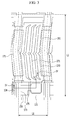
- FIG. 1 is a plan view illustrating a portion of a pixel area of an embodiment of a display device
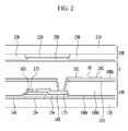
- FIG. 2 illustrates a cross-sectional view of a contact hole of a gate driver which is taken along a line II-II of the display device of FIG. 1 .
- a gate conductor including a gate line 121 is formed on an insulation substrate 110.
- the insulation substrate 110 may be made of transparent glass, plastic, or the like.
- the gate line 121 includes a gate electrode 124 and a wide end portion (not illustrated) for connection with another layer or an external driving circuit.
- the gate line 121 may be made of an aluminium-based metal such as aluminium (Al) or an aluminium alloy, a silver-based metal such as silver (Ag) or a silver alloy, a copper-based metal such as copper (Cu) or a copper alloy, a molybdenum-based metal such as molybdenum (Mo) or a molybdenum alloy, chromium (Cr), tantalum (Ta), or titanium (Ti).
- the gate line 121 may have a multilayered structure including at least two conductive layers having different physical properties.
- the gate insulating layer 140 may have a multilayered structure including at least two insulating layers having different physical properties.
- a semiconductor 154 made of amorphous silicon or polysilicon is formed on the gate insulating layer 140.
- the semiconductor 154 may further include an oxide semiconductor.
- Ohmic contacts 163 and 165 may be positioned on the semiconductor 154.
- the ohmic contacts 163 and 165 may be made of a material such as n+ hydrogenated amorphous silicon in which an n-type impurity such as phosphorus is doped at a high concentration, or of a silicide.
- the ohmic contacts 163 and 165 may form a pair to be disposed on the semiconductor 154. In the case where the semiconductor 154 is an oxide semiconductor, the ohmic contacts 163 and 165 may be omitted.
- the data line 171 includes a wide end portion (not illustrated) for connection with another layer or an external driving circuit.
- the data line 171 transfers a data signal and mainly extends in a vertical direction to cross the gate line 121.
- the data line 171 may have a first curved portion having a curved shape in order to acquire maximum transmittance of the liquid crystal display, and the curved portion meets another in a middle region of the pixel area to have a V-lettered shape.
- a second curved portion which is curved to form a predetermined angle with the first curved portion may be further included in the middle region of the pixel area.
- the first curved portion of the data line 171 may be bent at an angle of about 7° with respect to a vertical reference line which forms an angle of 90° with respect to a direction in which the gate line 121 is extended.
- the second curved portion disposed at the center area of the pixel area may be further bent to form an angle of about 7° to about 15° with respect to the first curved portion.
- the source electrode 173 is a part of the data line 171, and is disposed on the same line as the data line 171.
- the drain electrode 175 is formed to extend in parallel with the source electrode 173. Accordingly, the drain electrode 175 is parallel with a portion of the data line 171.
- the gate electrode 124, the source electrode 173, and the drain electrode 175 constitute one thin film transistor (TFT) together with the semiconductor 154, and a channel of the thin film transistor is positioned in the semiconductor 154 between the source electrode 173 and the drain electrode 175.
- TFT thin film transistor
- the liquid crystal display includes the source electrode 173 disposed on the same line as the data line 171, and the drain electrode 175 extended in parallel with the data line 171, thereby broadening the width of the thin film transistor without widening the area occupied by the data conductor and thus increasing the aperture ratio of the liquid crystal display.
- the data line 171 and the drain electrode 175 may be made of a refractory metal such as molybdenum, chromium, tantalum, and titanium, or an alloy thereof.
- the data line 171 and the drain electrode 175 may have a multilayer structure including a refractory metal layer (not shown) and a low resistance conductive layer (not shown).
- An example of the multilayered structure may include a double layer including a chromium, molybdenum, or molybdenum alloy lower layer and an aluminium or aluminium alloy upper layer, and a triple layer including a molybdenum or molybdenum alloy lower layer, an aluminium or aluminium alloy intermediate layer, and a molybdenum or molybdenum alloy upper layer.
- the data line 171 and the drain electrode 175 may be made of other various metals or conductors in addition to the described metals.
- a width of the data line 171 may be about 3.5 micrometers ( ⁇ m) ⁇ 0.75 ⁇ m
- a first passivation layer 180n is disposed on the data line 171, source electrode 173, drain electrode 175, the gate insulating layer 140, and the exposed semiconductor 154.
- the first passivation layer 180n may be formed of an organic insulating material or an inorganic insulating material.
- a second passivation layer 180q is disposed on the first passivation layer 180n.
- the second passivation layer 180q is optional and may be omitted.
- the second passivation layer 180q may be a color filter.
- the second passivation layer 180q may uniquely display one of the primary colors if it is the color filter, and the primary colors may be, for example, three primary colors such as red, green, and blue, or yellow, cyan, magenta, and the like.
- a color filter 230 for displaying mixed colors of the primary colors or white, as well as the primary colors may be further included.
- a second electrode 270 is formed on the second passivation layer 180q.
- the second electrode 270 may have a planar shape, and may be formed as a plate on the entire substrate 110.
- the second electrode 270 may have an opening (not illustrated) disposed in a region corresponding to a periphery of the drain electrode 175. That is, the second electrode 270 may have a plate-like plane shape.
- the second electrodes 270 positioned at adjacent pixels are connected to each other to receive a common voltage having a predetermined magnitude supplied from outside of the display area.
- a third passivation layer 180z is disposed on the second electrode 270.
- the third passivation layer 180z may be made of an organic insulating material, an inorganic insulating material, or the like.
- a first electrode 191 is formed on the third passivation layer 180z.
- the first electrode 191 includes a curved edge that is almost parallel to the first curved portion and the second curved portion of the data line 171.
- the first electrode 191 has a plurality of first cutouts 92, and includes a plurality of first slit electrodes 192 defined by the plurality of first cutouts 92.
- a first contact hole 185 exposing the drain electrode 175 is formed in the first passivation layer 180n, the second passivation layer 180q, and the third passivation layer 180z.
- the first electrode 191 is physically and electrically connected to the drain electrode 175 through the first contact hole 185 to receive a voltage from the drain electrode 175.
- an alignment layer is coated on the first electrode 191 and the third passivation layer 180z.
- the alignment layer may be a horizontal alignment layer and may be rubbed in a predetermined direction.
- the alignment layer may include a photoreactive material and may be photoaligned.
- the first electrode 191 may be a pixel electrode and the second electrode 270 may be a common electrode.
- the second display panel 200 will now be described.
- a light blocking member 220 is formed on an insulating substrate 210 made of transparent glass, plastic, or the like.
- the light blocking member 220 is also called a black matrix and serves to prevent light leakage.
- a plurality of color filters 230 are formed on the substrate 210.
- the color filter 230 of the upper display panel 200 may be omitted.
- the light blocking member 220 of the upper display panel 200 may also be formed in the lower display panel 100.
- An overcoat 250 is formed on the color filter 230 and the light blocking member 220.
- the overcoat 250 may be made of an insulating material (e.g. an organic insulating material), and prevents the color filter 230 from being exposed and provides a flat surface.
- the overcoat 250 is optional and may be omitted.
- An alignment layer (not shown) may be disposed on the overcoat 250.
- the liquid crystal layer 3 is interposed between the lower display panel 100 and the upper display panel 200.
- the liquid crystal layer 3 may include the liquid crystal composition described above. Long axes of liquid crystal molecules of the liquid crystal layer 3 may be horizontally aligned with respect to surfaces of the two display panels 100 and 200 in a state where there is no electric field applied to the liquid crystal display.
- the liquid crystal layer includes a liquid crystal composition including one or more kinds of the compound represented by Chemical Formula 1.
- n 0, 1, or 2
- (R 1 ) is hydrogen or a C1 to C15 alkyl.
- the element represented by X is F, Cl, CF 3 , CF 2 CF 3 , CHF 2 , CH 2 F, OCF 3 , CN, NCS, or a C1 to C5 alkyl including 1 to 3 elements represented by F.
- a CH 2 group may be independently substituted with ( i.e. optionally replaced with) one or more oxygen atoms.
- (F) indicates that the fluoro group may be substituted or unsubstituted.
- the compound represented by Chemical Formula 1 may include one or more the compounds represented by Chemical Formula 1-1 to Chemical Formula 1-14.
- an appropriate content of the compound represented by Chemical Formula 1 may be in a range of about 1 wt% to about 30 wt% (of the total weight of the liquid crystal composition). More specifically, the content may be in a range of about 5 wt% to about 20 wt%, or even more specifically, may be in a range of about 5 wt% to about 15 wt%.
- the low temperature stability may be reduced.
- the liquid crystal composition may further include one or more of the compound represented by Chemical Formula 2.
- R 1 and R 2 independently indicate C1 to C12 alkyl, C1 to C12 alkoxy, or C2 to C12 alkenyl.
- a content of the compound represented by Chemical Formula 2 may be in a range of about 5 wt% to about 60 wt% of the total weight of the liquid crystal composition. More specifically, the compound of Chemical Formula 2 may be in a range of about 10 wt% to about 60 wt%, about 20 wt% to about 60 wt%, about 20 wt% to about 50 wt% or about 30 wt% to about 50 wt% or even more specifically, may be in a range of about 40 wt% to about 50 wt% or about 45 wt% to about 50 wt% of the total weight of the liquid crystal composition.
- the liquid crystal composition may include one or more of the compound represented by Chemical Formula 3.
- R 3 and R 4 independently indicate C1 to C12 alkyl, C1 to C12 alkoxy, or C2 to C12 alkenyl.
- a content of the compound represented by Chemical Formula 3 may be in a range of about 1 wt% to about 40 wt%. More specifically, the compound of Chemical Formula 3 may be in a range of about 5 wt% to about 40 wt%, about 10 wt% to about 40 wt% or about 10 wt% to about 30 wt%, or even more specifically, may be in a range of about 15 wt% to about 30 wt% of the total weight of the liquid crystal composition.
- the liquid crystal composition may further include one or more of the compound represented by Chemical Formula 4.
- R 5 indicates C1 to C12 alkyl, C1 to C12 alkoxy, or C2 to C12 alkenyl, and (F) indicates that a fluoro may be substituted or unsubstituted.
- a content of the compound represented by Chemical Formula 4 may be in a range of about 1 wt% to about 40 wt% of the total weight of the liquid crystal composition. More specifically, the compound of Chemical Formula 4 may be in a range of about 5 wt% to about 40 wt%, about 5 wt% to about 30 wt%, or even more specifically, may be in a range of about 5 wt% to about 25 wt% of the total weight of the liquid crystal composition.
- the liquid crystal composition may further include one or more of the compound represented by Chemical Formula 5.
- R 6 indicates C1 to C12 alkyl, C1 to C12 alkoxy, or C2 to C12 alkenyl.
- a content of the compound represented by Chemical Formula 5 may be in a range of about 1 wt% to about 15 wt% of the total weight of the liquid crystal composition. More specifically, the compound of Chemical Formula 5 may be in a range of about 1 wt% to about 10 wt%, or about 2 wt% to about 10 wt% or even more specifically, may be in a range of about 3 wt% to about 10 wt%, about 3 wt% to about 9 wt% or about 3 wt% to about 8 wt% of the total weight of the liquid crystal composition.
- the liquid crystal composition includes the compound represented by Chemical Formula 1, and may further include all of the compounds represented by Chemical Formulae 2 to 5, or may further include only some of the compounds represented by Chemical Formulae 2 to 5.
- the first electrode 191 is disposed on the second electrode 270.
- the second electrode 270 is disposed on the first electrode 191.
- FIG. 3 is a plan view of a liquid crystal display
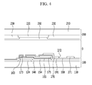
- FIG. 4 is a cross-sectional view taken along a line IV-IV of the exemplary embodiment illustrated in FIG. 3 .
- the liquid crystal display is substantially similar to the liquid crystal display illustrated in FIG. 1 and FIG. 2 .
- a gate line 121 is formed on an insulation substrate 110.
- a gate insulating layer 140 is formed on the gate line 121 that is formed of a silicon nitride (SiNx) or a silicon oxide (SiOx).
- a semiconductor 154 is formed on the gate insulating layer 140.
- Ohmic contacts 163 and 165 are formed on the semiconductor 154.
- the ohmic contacts 163 and 165 may be omitted.
- a data conductor including a data line 171, a source electrode 173, and a drain electrode 175 is formed on the ohmic contacts 163 and 165 and the gate insulating layer 140.
- a first electrode 191 is formed directly on the drain electrode 175.
- the first electrode 191 has a planar shape, which is a plate shape, and is disposed in one pixel area.
- a passivation layer 180 is disposed on the data conductors 171, 173, and 175, the gate insulating layer 140, exposed portions of the semiconductor 154, and the first electrode 191.
- a passivation layer 180 may be disposed between the first electrode 191 and the data line 171, and the first electrode 191 may be connected to the drain electrode 175 through a contact hole 185 formed in the passivation layer 180.
- the second electrode 270 is formed on the passivation layer 180. Second electrodes 270 are connected to each other to receive common voltages from a common voltage applying unit that is disposed outside of the display area.
- the second electrode 270 includes the curved edge which is substantially parallel to the first curved portion and the second curved portion of the data line 171, and the second electrodes 270 disposed at the adjacent pixels are connected to each other.
- the second electrode 270 includes a plurality of second cutouts 272 and a plurality of second branch electrodes 271 defined by the plurality of second cutouts 272.
- an alignment layer may be coated on the first electrode 191 and the passivation layer 180.
- the alignment layer may be a horizontal alignment layer and be rubbed in a predetermined direction
- the alignment layer may include a photoreactive material to be photoaligned.
- the upper display panel 200 will now be described.
- a light blocking member 220 is formed on an insulating substrate 210.
- a plurality of color filters 230 are formed on the substrate 210.
- the color filters 230 may be disposed on the lower display panel 100, and in this case, the light blocking member 220 may also be disposed on the lower display panel 100.
- An overcoat 250 is formed on the color filter 230 and the light blocking member 220.
- the overcoat 250 may be omitted.
- the alignment layer may be disposed on the overcoat 250.
- the liquid crystal layer 3 is interposed between the lower display panel 100 and the upper display panel 200.
- the liquid crystal layer 3 may include the liquid crystal composition which has been previously described. Detailed description of the same constituent elements of the liquid crystal composition is omitted.
- the liquid crystal layer includes one or more of the compound represented by Chemical Formula 1.
- n 0, 1, or 2
- (R 1 ) is hydrogen or a C1 to C15 alkyl.
- a substituent represented by "X” is F, Cl, CF 3 , CF 2 CF 3 , CHF 2 , CH 2 F, OCF 3 , CN, NCS, or a C1 to C5 alkyl including 1 to 3 elements represented by F.
- a CH 2 group of the C1 to C5 alkyl may be independently substituted with ( i.e. optionally replaced with) an oxygen atom.
Landscapes
- Chemical & Material Sciences (AREA)
- Organic Chemistry (AREA)
- Physics & Mathematics (AREA)
- Crystallography & Structural Chemistry (AREA)
- Engineering & Computer Science (AREA)
- Materials Engineering (AREA)
- Nonlinear Science (AREA)
- Mathematical Physics (AREA)
- General Physics & Mathematics (AREA)
- Optics & Photonics (AREA)
- Geometry (AREA)
- Microelectronics & Electronic Packaging (AREA)
- Liquid Crystal Substances (AREA)
- Liquid Crystal (AREA)
Abstract
Description
- The present invention relates to a compound, a liquid crystal composition including the compound, and a liquid crystal display including the liquid crystal composition.
- Liquid crystal displays are widely used as one of flat panel displays. The liquid crystal display determines a direction of the liquid crystal molecules within the liquid crystal layer and controls transmittance of light passing through the liquid crystal layer by applying a voltage to the field generating electrodes to generate an electric field in the liquid crystal layer.
- The liquid crystal enables the liquid crystal display to achieve a desired image by controlling the transmittance of light. In particular, with different uses of liquid crystal displays, various characteristics of the liquid crystal are optimized, such as low-voltage driving, a high voltage holding ratio (VHR), a wide viewing angle, a wide operation temperature range, and high-speed response.
- In order to obtain high-speed response characteristics for a liquid crystal display, studies for improving the physical properties of the liquid crystal composition, such as rotational viscosity, refractive index, and elastic coefficient, are in progress.
- The above information disclosed in this Background section is only for enhancement of understanding of the background of the invention and therefore it may contain information that does not form the prior art that is already known to a person of ordinary skill in the art.
- Disclosed herein are a liquid crystal composition and a display device including the same, capable of realizing high speed response characteristics and low temperature stability.
- An embodiment provides a liquid crystal composition including a compound represented by Chemical Formula 1:


(R1) is hydrogen or a C1 to C15 alkyl, in which at least one CH2 group is optionally independently replaced with -C≡C-, -CF2O-, -CH=CH-, -O-, -CO-O-, -O-CO-, or -O-CO-O- in a way that oxygen atoms are directly connected to each other, and 1 to 3 hydrogen atoms are optionally replaced with halogen,
(F) indicates that a fluoro may be substituted or unsubstituted (i.e. optionally substituted in place of hydrogen), and
each of


- In an embodiment, a liquid crystal composition including the compound represented by Chemical Formula 1 may include one of more compounds represented by Chemical Formula 1-1 to Chemical Formula 1-14.


- In an embodiment, the content of the compound represented by Chemical Formula 1 may be in a range of about 1 wt% to about 30 wt% of the total weight of the liquid crystal composition.
- In an embodiment, the liquid crystal composition may further include one or more of the compound represented by Chemical Formula 2.

- In Chemical Formula 2, R1 and R2 may independently indicate C1 to C12 alkyl, C1 to C12 alkoxy, or C2 to C12 alkenyl.
- In an embodiment, a content of the compound represented by Chemical Formula 2 may be in a range of about 5 wt% to about 60 wt% of the total liquid crystal composition.
- In an embodiment, the liquid crystal composition may further include one or more of the compound represented by Chemical Formula 3:

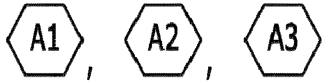


- In an embodiment, a content of the compound represented by Chemical Formula 3 may be in a range of about 1 wt% to about 40 wt% of the total weight of the liquid crystal composition.
- In an embodiment, the liquid crystal composition may further include one or more of the compound represented by Chemical Formula 4:


- In an embodiment, a content of the compound represented by Chemical Formula 4 may be in a range of about 1 wt% to about 40 wt%.
- The liquid crystal composition further includes one or more of the compound represented by Chemical Formula 5:
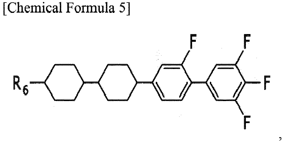
- In an embodiment, a content of the compound represented by Chemical Formula 5 may be in a range of about 1 wt% to about 15 wt% of the total weight of the liquid crystal composition.
- An embodiment provides a liquid crystal display including: a first insulation substrate; a thin film transistor disposed on the first insulation substrate; a first electrode connected to the thin film transistor; a second electrode disposed on the first insulation substrate while being insulated from the first electrode; a second insulation substrate configured to face the first insulation substrate; and a liquid crystal layer disposed between the first insulation substrate and the second insulation substrate, wherein the liquid crystal layer includes a liquid crystal composition including a compound represented by Chemical Formula 1:

(R1) is hydrogen or a C1 to C15 alkyl, in which at least one CH2 group is optionally independently replaced with -C≡C-, -CF2O-, -CH=CH-, -O-, -CO-O-, -O-CO-, or -O-CO-O- in a way that oxygen atoms are directly connected to each other, and 1 to 3 hydrogen atoms are optionally replaced with a halogen;
(F) indicates that a fluoro may be substituted or unsubstituted; and each of


- In an exemplary embodiment, the compound represented by Chemical Formula 1 may include one or more compounds represented by Chemical Formula 1-1 to Chemical Formula 1-14.



- In an embodiment, a content of the compound represented by Chemical Formula 1 may be in a range of about 1 wt% to about 30 wt% of the total weight of the liquid crystal composition.
- In an embodiment, the liquid crystal composition may include one or more of the compound represented by Chemical Formula 2.

- In Chemical Formula 2, R1 and R2 may independently indicate C1 to C12 alkyl, C1 to C12 alkoxy, or C2 to C12 alkenyl.
- In an embodiment, a content of the compound represented by Chemical Formula 2 may be in a range of about 5 wt% to about 60 wt% of the total weight of the liquid crystal composition.
- An embodiment provides a liquid crystal display including: a first insulation substrate; a thin film transistor disposed on the first insulation substrate; a first electrode connected to the thin film transistor; a second electrode disposed on the first insulation substrate while being insulated from the first electrode; a second insulation substrate configured to face the first insulation substrate; and a liquid crystal layer disposed between the first insulation substrate and the second insulation substrate, wherein the liquid crystal layer includes a liquid crystal composition as described herein.
- At least some of the above and other features of the invention are set out in the claims. According to the embodiments disclosed herein, it is possible to improve the performance of a liquid crystal display by manufacturing the liquid crystal display using a liquid crystal composition including the exemplary compound.
- The above and other advantages and features of this disclosure will become more apparent by describing in further detail embodiments thereof with reference to the accompanying drawings, in which:
-
FIG. 1 is a plan view illustrating a portion of a pixel area of an embodiment of a display device. -
FIG. 2 illustrates a cross-sectional view of a contact hole of a gate driver of an embodiment of a display device, which is taken along a line II-II of the plan view ofFIG. 1 . -
FIG. 3 is a plan view illustrating an embodiment of a display device. -
FIG. 4 is a cross-sectional view illustrating the display device taken along a line IV-IV according to the embodiment illustrated inFIG. 3 . - The present invention will now be described more fully hereinafter with reference to the accompanying drawings, in which embodiments are shown. As those skilled in the art would realize, the described embodiments may be modified in various different ways, all without departing from the scope of the present invention.
- In the drawings, the thickness of layers, films, panels, regions, etc., are exaggerated for clarity. Like reference numerals designate like elements throughout the specification. It will be understood that when an element such as a layer, film, region, or substrate is referred to as being "on" another element, it can be directly on the other element or intervening elements may also be present. In contrast, when an element is referred to as being "directly on" another element, there are no intervening elements present.
- It will be understood that, although the terms "first," "second," "third" etc. may be used herein to describe various elements, components, regions, layers and/or sections, these elements, components, regions, layers and/or sections should not be limited by these terms. These terms are only used to distinguish one element, component, region, layer or section from another element, component, region, layer or section. Thus, "a first element," "component," "region," "layer" or "section" discussed below could be termed a second element, component, region, layer or section without departing from the teachings herein.
- The terminology used herein is for the purpose of describing particular embodiments only and is not intended to be limiting. As used herein, the singular forms "a," "an," and "the" are intended to include the plural forms, including "at least one," unless the content clearly indicates otherwise. "Or" means "and/or." As used herein, the term "and/or" includes any and all combinations of one or more of the associated listed items. It will be further understood that the terms "comprises" and/or "comprising," or "includes" and/or "including" when used in this specification, specify the presence of stated features, regions, integers, steps, operations, elements, and/or components, but do not preclude the presence or addition of one or more other features, regions, integers, steps, operations, elements, components, and/or groups thereof.
- Furthermore, relative terms, such as "lower" or "bottom" and "upper" or "top," may be used herein to describe one element's relationship to another element as illustrated in the Figures. It will be understood that relative terms are intended to encompass different orientations of the device in addition to the orientation depicted in the Figures. For example, if the device in one of the figures is turned over, elements described as being on the "lower" side of other elements would then be oriented on "upper" sides of the other elements. The term "lower," can therefore, encompass both an orientation of "lower" and "upper," depending on the particular orientation of the figure. Similarly, if the device in one of the figures is turned over, elements described as "below" or "beneath" other elements would then be oriented "above" the other elements. The terms "below" or "beneath" can, therefore, encompass both an orientation of above and below.
- "About" or "approximately" as used herein is inclusive of the stated value and means within an acceptable range of deviation for the particular value as determined by one of ordinary skill in the art, considering the measurement in question and the error associated with measurement of the particular quantity (i.e., the limitations of the measurement system). For example, "about" can mean within one or more standard deviations, or within ± 30%, 20%, 10%, or 5% of the stated value.
- Unless otherwise defined, all terms (including technical and scientific terms) used herein have the same meaning as commonly understood by one of ordinary skill in the art to which this disclosure belongs. It will be further understood that terms, such as those defined in commonly used dictionaries, should be interpreted as having a meaning that is consistent with their meaning in the context of the relevant art and the present disclosure, and will not be interpreted in an idealized or overly formal sense unless expressly so defined herein.
- Embodiments are described herein with reference to cross section illustrations that are schematic illustrations of embodiments. As such, variations from the shapes of the illustrations as a result, for example, of manufacturing techniques and/or tolerances, are to be expected. Thus, embodiments described herein should not be construed as limited to the particular shapes of regions as illustrated herein but are to include deviations in shapes that result, for example, from manufacturing. For example, a region illustrated or described as flat may, typically, have rough and/or nonlinear features. Moreover, sharp angles that are illustrated may be rounded. Thus, the regions illustrated in the figures are schematic in nature and their shapes are not intended to illustrate the precise shape of a region and are not intended to limit the scope of the present claims.
- Compounds are described using standard nomenclature. For example, any position not substituted by any indicated group is understood to have its valency filled by a bond as indicated, or a hydrogen atom. A dash ("-") that is not between two letters or symbols is used to indicate a point of attachment for a substituent. For example, -CHO is attached through carbon of the carbonyl group.
- An "alkyl" group as used herein means a C1 to C12 straight or branched chain hydrocarbon that is unsubstituted, or substituted with 1 to 3 F, Cl, CF3, CF2CF3, CHF2, CH2F, OCF3, CN, NCS or a combination thereof, preferably a C1 to C8 straight or branched chain hydrocarbon that is unsubstituted, or substituted with 1 to 3 of F, Cl, CF3, CF2CF3, CHF2, CH2F, OCF3, CN, NCS, or a combination thereof, more preferably a C1 to C4 straight or branched chain hydrocarbon that is unsubstituted, or substituted with 1 to 3 of F, or 1 of Cl, CF3, CF2CF3, CHF2, CH2F, OCF3, CN, NCS.
- An "alkyloxy" or "alkoxy" group as used herein means an alkyl group as defined above attached to a carbon atom via an ether oxygen.
- An "alkenyl" group as used herein means a C2 to C12 straight or branched chain hydrocarbon having one or more unsaturations, and that is unsubstituted, or substituted with 1 to 3 of F, Cl, CF3, CF2CF3, CHF2, CH2F, OCF3, CN, NCS, or a combination thereof, preferably a C2 to C8 straight or branched chain hydrocarbon that is unsubstituted, or substituted with 1 to 3 of F, Cl, CF3, CF2CF3, CHF2, CH2F, OCF3, CN, or a combination thereof, more preferably a C2 to C4 straight or branched chain hydrocarbon that is unsubstituted, or substituted with 1 to 3 of F, Cl, CF3, CF2CF3, CHF2, CH2F, OCF3, or CN.
- The number of carbon atoms of a group is independent of the number of substituents. For example a CH2CH2CF2CF3 group is a C2 alkyl substituted with CF2CF3.
- Hereinafter, a compound, a liquid crystal composition including the compound, and a liquid crystal display including the liquid crystal composition will be described in detail with reference to the accompanying drawings.
- In an embodiment, a compound is represented by Chemical Formula 1.

- In Chemical Formula 1, n is 0, 1, or 2, and (R1) is hydrogen or a C1 to C15 alkyl (e.g. a C1 to C10 alkyl or a C1 to C5 alkyl such as a C1 alkyl). In this case, at least one CH2 group of the C1 to C 15 alkyl may be independently replaced with -C≡C-, -CF2O-, -CH=CH-, -O-, -CO-O-, -O-CO-, or -O-CO-O- in a way that oxygen atoms, if present, are directly connected to each other, and 1 to 3 hydrogen atoms may be replaced with a halogen. In an embodiment when (R1) is a C1 alkyl, the C1 alkyl may be CH3.
- The element represented by "X" is F, Cl, CF3, CF2CF3, CHF2, CH2F, OCF3, CN, NCS, or a C1 to C5 alkyl including 1 to 3 elements represented by F. In this regard, when X is a C1 to C5 alkyl including 1 to 3 fluoro substituents, a CH2 group may be independently substituted with (i.e. optionally replaced with) one or more oxygen atoms. In some embodiments, "X" is F, CF3 or OCF3.
- (F) indicates that fluoro may be substituted or unsubstituted. In other words, (F) indicates that fluoro is optionally substituted in place of hydrogen.
- Each of


- The compound represented by Chemical Formula 1 may include one or more compounds represented by Chemical Formula 1-1 to Chemical Formula 1-14.


- A process of manufacturing the compound represented by Chemical Formula 1-1 may be schematized as follows.

- Further, a process of manufacturing the compound represented by Chemical Formula 1-2 may be schematized as follows.

- A process of manufacturing the compound represented by Chemical Formula 1-8 may be schematized as follows.

- Although the manufacturing processes for some of the compounds represented by Chemical Formula 1 have been schematized, the manufacturing processes are not limited thereto.
- These new compounds may have advantageous rotational viscosity characteristics when applied to a liquid crystal composition as compared with a compound having a conventional structure. Without being limited by theory, it is believed that the improved rotational viscosity may be attributed to the inclusion of a methyl substituent in a meta direction (i.e. meta position) of a phenyl group. This will be described later in detail.
- Hereinafter, an embodiment of a liquid crystal composition will be described. The liquid crystal composition includes one or more compound represented by Chemical Formula 1.

- The element represented by X is F, Cl, CF3, CF2CF3, CHF2, CH2F, OCF3, CN, NCS, or a C1 to C5 alkyl including 1 to 3 elements represented by F. In this regard, a CH2 group of the C1 to C5 alkyl may be independently substituted with (i.e. optionally replaced with) one or more oxygen atoms.
- (F) indicate that a fluoro may be substituted or unsubstituted.
- Each of


- The compound represented by Chemical Formula 1 may include one of more compounds represented by Chemical Formula 1-1 to Chemical Formula 1-14.


- In a total liquid crystal composition, the content of the compound represented by Chemical Formula 1 may be in a range of about 1 wt% to about 30 wt% (of the total weight of the liquid crystal composition). More specifically, the compound of Chemical Formula 1 may be in a range of about 5 wt% to about 20 wt%, or even more specifically, may be in a range of about 5 wt% to about 15 wt% of the total weight of the liquid crystal composition.
- If the content of the compound represented by Chemical Formula 1 is less than about 1 wt% of the total liquid crystal composition, it is difficult to achieve a low viscosity effect.
- Further, if the content of the compound represented by Chemical Formula 1 exceeds about 30 wt% of the total liquid crystal composition, low temperature stability may be reduced.
- The liquid crystal composition may include one or more of the compounds represented by Chemical Formula 2.

- In Chemical Formula 2, R1 and R2 independently indicate C1 to C12 alkyl, C1 to C12 alkoxy, or C2 to C12 alkenyl.
- A content of the compound represented by Chemical Formula 2 may be in a range of about 5 wt% to about 60 wt% of the total liquid crystal composition. More specifically, the compound of Chemical Formula 2 may be in a range of about 10 wt% to about 60 wt%, about 20 wt% to about 60 wt%, about 20 wt% to about 50 wt% or about 30 wt% to about 50 wt% or even more specifically, may be in a range of about 40 wt% to about 50 wt% or about 45 wt% to about 50 wt% of the total weight of the liquid crystal composition.
- The liquid crystal composition may include one or more of the compound represented by
Chemical Formula 3.


- (F) indicates that a fluoro is optionally substituted in place of a hydrogen, R3 and R4 independently indicate C1 to C12 alkyl, C1 to C12 alkoxy, or C2 to C12 alkenyl.
- A content of the compound represented by
Chemical Formula 3 may be in a range of about 1 wt% to about 40 wt% of the total liquid crystal composition. More specifically, the compound ofChemical Formula 3 may be in a range of about 5 wt% to about 40 wt%, about 10 wt% to about 40 wt% or about 10 wt% to about 30 wt%, or even more specifically, may be in a range of about 15 wt% to about 30 wt% of the total weight of the liquid crystal composition. - The liquid crystal composition may include one or more of the compound represented by Chemical Formula 4.

- Each of


- R5 indicates C1 to C12 alkyl, C1 to C12 alkoxy, or C2 to C12 alkenyl, and (F) indicates that a fluoro may be substituted or unsubstituted.
- A content of the compound represented by Chemical Formula 4 may be in a range of about 1 wt% to about 40 wt% of the total liquid crystal composition. More specifically, the compound of Chemical Formula 4 may be in a range of about 5 wt% to about 40 wt%, about 5 wt% to about 30 wt%, or even more specifically, may be in a range of about 5 wt% to about 25 wt% of the total weight of the liquid crystal composition.
- The liquid crystal composition may include one or more of the compound represented by Chemical Formula 5.

- R6 indicates C1 to C12 alkyl, C1 to C12 alkoxy, or C2 to C12 alkenyl.
- A content of the compound represented by Chemical Formula 5 may be in a range of about 1 wt% to about 15 wt% of the total liquid crystal composition. More specifically, the compound of Chemical Formula 5 may be in a range of about 1 wt% to about 10 wt%, or about 2 wt% to about 10 wt% or even more specifically, may be in a range of about 3 wt% to about 10 wt%, about 3 wt% to about 9 wt% or about 3 wt% to about 8 wt% of the total weight of the liquid crystal composition.
- In an embodiment, the liquid crystal composition includes the compound represented by Chemical Formula 1, and may further include all of the compounds represented by Chemical Formulae 2 to 5, or may further include only some of the compounds represented by Chemical Formulae 2 to 5.
- In other words, the liquid crystal composition necessarily includes the compound represented by Chemical Formula 1, and may further optionally include the compounds represented by Chemical Formulae 2 to 5 in an appropriate ratio as needed.
- Hereinafter, of the properties of the liquid crystal compound will be described.
- The phase transition temperature (Tni), refractive index Δn, dielectric anisotropy (Δε), and rotational viscosity (γ1) were measured for two new compounds (Examples 1 and 2) and three comparative example compounds (Comparative Examples 1-3).
(Table 1) Structure Tni Δn Δε γ1 3 ring Comparative Example 1 
48 0.21 20 156 Comparative Example 2 
0 0.13 23 102 Example 1 (Chemical Formula 1-1) 
51 0.08 19 96 4 ring Comparative Example 3 
99 0.20 31 232 Example 2 (Chemical Formula 1-8) 
66 0.17 20 148 - As shown in Table 1, the rotational viscosity is reduced in the compounds of Examples 1 and 2 as compared with the compounds of Comparative Examples 1 to 3.
- Referring to Table 1, the structure of the compounds according to Examples 1 and 2 includes a methyl substituent attached to a phenyl group in the meta direction (i.e. meta position). However, the methyl substituent is not included in the compounds of the comparative examples.
- For example, when the compound includes 3-ring structures, the rotation viscosity is reduced in the compound including the methyl substituent in the meta direction as represented by Chemical Formula 1-1 (Example 1) when compared with the compounds according to Comparative Examples 1 and 2.
- Similarly, in the case of a compound including 4-ring structures, the rotation viscosity is significantly ameliorated in the compound including the methyl substituent as represented by Chemical Formula 1-8 (Example 2) when compared with the compound according to Comparative Example 3.
- Hereinafter, a result of measuring the property of an embodiment of a liquid crystal composition will be described.
- Table 2 shows properties of the liquid crystal compositions according to Comparative Example 2 and Examples 4 to 6. Further, Table 3 shows the structure and amount of each compound included in the liquid crystal compositions according to Comparative Example 2 and Examples 4-6.
(Table 2) Property Comparative Example 2 (C2) Example 4 (E4) Example 5 (E5) Example 6 (E6) Dielectric anisotropy (Δε), 4.5 4.6 4.4 4.3 Tni 79 78 79 74 Δn 0.110 0.110 0.110 0.110 rotation viscosity (γ1) 53 46 44 45 (Table 3) Single group (Content, wt %) R1 R2 C2 (wt%) E4 (wt%) E5 (wt%) E6 (wt%) 1 
- - 36.2 38.1 38.0 39.0 2 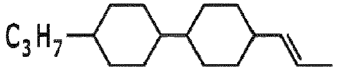
- - 9.4 10.8 9.0 8.0 3 
C3H7 C2H5 4.5 4.3 4.0 3.0 C5H11 C2H5 4.2 3.9 4.0 - 4 
- - 5.2 4.9 6.2 4.5 5 
C2H5 C3H7 2.6 4.3 6.0 2.8 C3H7 C3H7 1.6 3.1 - - 6 
C2H5 - - - 6.8 9.7 C3H7 - - - - 4.9 7 
C2H5 - 2.4 6.3 - - C3H7 - 7.5 3.9 - - C5H11 - 8.0 - - - 8 
- - - 7.5 9.0 5.0 9 
- - - - 3.0 4.0 10 
- - 5 - 4.0 8.3 11 
- - 4.5 6.2 2.0 7.5 12 
- - 7.0 - - - 13 
- - 2.1 6.7 8.0 3.3 - Referring to Table 2, the rotation viscosity (γ1) is ameliorated in the liquid crystal composition including the compound represented by Chemical Formula 1 (according to Examples 4 to 6) while it still has the same levels of Tni, Δn, and dielectric anisotropy (Δε) as the liquid crystal composition of Comparative Example 2.
- Table 3 shows the structure and the amount of individual liquid crystal compounds included in the liquid crystal compositions for each of the comparative examples and examples. Referring to Table 3, the liquid crystal composition according to the Examples may have a reduced total amount of the terphenyl-based (#7) liquid crystal single groups (Example 4) or no terphenyl-based (#7) liquid crystal single group (Examples 5 and 6).
- However, referring to Table 2, as shown in the Examples, it is possible to ameliorate the rotation viscosity characteristic of the liquid crystal composition while having the same or similar level of dielectric anisotropicity by reducing the content of the terphenyl-based liquid crystal single group or by not including the terphenyl-based liquid crystal single group in the liquid crystal composition.
- In brief, since having high dielectric anisotropy, the terphenyl-based compound generally needs to be included in the liquid crystal composition at a predetermined ratio. However, in the present embodiment, when the liquid crystal composition includes the compound represented by Chemical Formula 1, it is possible to maintain the same or improved characteristics while simultaneously reducing the content of the terphenyl-based liquid crystal single group.
- Specifically, it is possible to accomplish the same or similar performance by using a single compound substituted with a methyl group at a meta position (i.e. the compound represented by Chemical Formula 1) without the need to include a terphenyl-based compound which is typically used as an essential component of a conventional liquid crystal composition.
- Hereinafter, a liquid crystal display including the above-described liquid crystal composition will be described with reference to
FIG. 1 andFIG. 2 . However, the structure of the liquid crystal display to be described below is merely an example, and the liquid crystal composition may be applied to alternative structures of the liquid crystal display. -
FIG. 1 is a plan view illustrating a portion of a pixel area of an embodiment of a display device, andFIG. 2 illustrates a cross-sectional view of a contact hole of a gate driver which is taken along a line II-II of the display device ofFIG. 1 . - A gate conductor including a
gate line 121 is formed on aninsulation substrate 110. Theinsulation substrate 110 may be made of transparent glass, plastic, or the like. - The
gate line 121 includes agate electrode 124 and a wide end portion (not illustrated) for connection with another layer or an external driving circuit. Thegate line 121 may be made of an aluminium-based metal such as aluminium (Al) or an aluminium alloy, a silver-based metal such as silver (Ag) or a silver alloy, a copper-based metal such as copper (Cu) or a copper alloy, a molybdenum-based metal such as molybdenum (Mo) or a molybdenum alloy, chromium (Cr), tantalum (Ta), or titanium (Ti). Thegate line 121 may have a multilayered structure including at least two conductive layers having different physical properties. - A
gate insulating layer 140 made of a silicon nitride (SiNx), a silicon oxide (SiOx), or the like, is formed on thegate line 121. Thegate insulating layer 140 may have a multilayered structure including at least two insulating layers having different physical properties. - A
semiconductor 154 made of amorphous silicon or polysilicon is formed on thegate insulating layer 140. Thesemiconductor 154 may further include an oxide semiconductor. -
Ohmic contacts semiconductor 154. Theohmic contacts ohmic contacts semiconductor 154. In the case where thesemiconductor 154 is an oxide semiconductor, theohmic contacts - A data conductor including a
data line 171, asource electrode 173 and adrain electrode 175, is formed on theohmic contacts gate insulating layer 140. - The
data line 171 includes a wide end portion (not illustrated) for connection with another layer or an external driving circuit. Thedata line 171 transfers a data signal and mainly extends in a vertical direction to cross thegate line 121. - In this case, the
data line 171 may have a first curved portion having a curved shape in order to acquire maximum transmittance of the liquid crystal display, and the curved portion meets another in a middle region of the pixel area to have a V-lettered shape. A second curved portion which is curved to form a predetermined angle with the first curved portion may be further included in the middle region of the pixel area. - The first curved portion of the
data line 171 may be bent at an angle of about 7° with respect to a vertical reference line which forms an angle of 90° with respect to a direction in which thegate line 121 is extended. The second curved portion disposed at the center area of the pixel area may be further bent to form an angle of about 7° to about 15° with respect to the first curved portion. - The
source electrode 173 is a part of thedata line 171, and is disposed on the same line as thedata line 171. Thedrain electrode 175 is formed to extend in parallel with thesource electrode 173. Accordingly, thedrain electrode 175 is parallel with a portion of thedata line 171. - The
gate electrode 124, thesource electrode 173, and thedrain electrode 175 constitute one thin film transistor (TFT) together with thesemiconductor 154, and a channel of the thin film transistor is positioned in thesemiconductor 154 between thesource electrode 173 and thedrain electrode 175. - In an embodiment, the liquid crystal display includes the
source electrode 173 disposed on the same line as thedata line 171, and thedrain electrode 175 extended in parallel with thedata line 171, thereby broadening the width of the thin film transistor without widening the area occupied by the data conductor and thus increasing the aperture ratio of the liquid crystal display. - The
data line 171 and thedrain electrode 175 may be made of a refractory metal such as molybdenum, chromium, tantalum, and titanium, or an alloy thereof. Thedata line 171 and thedrain electrode 175 may have a multilayer structure including a refractory metal layer (not shown) and a low resistance conductive layer (not shown). An example of the multilayered structure may include a double layer including a chromium, molybdenum, or molybdenum alloy lower layer and an aluminium or aluminium alloy upper layer, and a triple layer including a molybdenum or molybdenum alloy lower layer, an aluminium or aluminium alloy intermediate layer, and a molybdenum or molybdenum alloy upper layer. However, thedata line 171 and thedrain electrode 175 may be made of other various metals or conductors in addition to the described metals. A width of thedata line 171 may be about 3.5 micrometers (μm) ± 0.75 μm. - A
first passivation layer 180n is disposed on thedata line 171,source electrode 173,drain electrode 175, thegate insulating layer 140, and the exposedsemiconductor 154. Thefirst passivation layer 180n may be formed of an organic insulating material or an inorganic insulating material. - A
second passivation layer 180q is disposed on thefirst passivation layer 180n. Thesecond passivation layer 180q is optional and may be omitted. Thesecond passivation layer 180q may be a color filter. Thesecond passivation layer 180q may uniquely display one of the primary colors if it is the color filter, and the primary colors may be, for example, three primary colors such as red, green, and blue, or yellow, cyan, magenta, and the like. Although not illustrated, acolor filter 230 for displaying mixed colors of the primary colors or white, as well as the primary colors, may be further included. - A
second electrode 270 is formed on thesecond passivation layer 180q. Thesecond electrode 270 may have a planar shape, and may be formed as a plate on theentire substrate 110. Thesecond electrode 270 may have an opening (not illustrated) disposed in a region corresponding to a periphery of thedrain electrode 175. That is, thesecond electrode 270 may have a plate-like plane shape. - The
second electrodes 270 positioned at adjacent pixels are connected to each other to receive a common voltage having a predetermined magnitude supplied from outside of the display area. - A
third passivation layer 180z is disposed on thesecond electrode 270. Thethird passivation layer 180z may be made of an organic insulating material, an inorganic insulating material, or the like. - A
first electrode 191 is formed on thethird passivation layer 180z. Thefirst electrode 191 includes a curved edge that is almost parallel to the first curved portion and the second curved portion of thedata line 171. Thefirst electrode 191 has a plurality offirst cutouts 92, and includes a plurality offirst slit electrodes 192 defined by the plurality offirst cutouts 92. - A
first contact hole 185 exposing thedrain electrode 175 is formed in thefirst passivation layer 180n, thesecond passivation layer 180q, and thethird passivation layer 180z. Thefirst electrode 191 is physically and electrically connected to thedrain electrode 175 through thefirst contact hole 185 to receive a voltage from thedrain electrode 175. - Although not illustrated, an alignment layer is coated on the
first electrode 191 and thethird passivation layer 180z. The alignment layer may be a horizontal alignment layer and may be rubbed in a predetermined direction. However, in accordance with another embodiment of a liquid crystal display, the alignment layer may include a photoreactive material and may be photoaligned. - The
first electrode 191 may be a pixel electrode and thesecond electrode 270 may be a common electrode. - The
second display panel 200 will now be described. - A
light blocking member 220 is formed on an insulatingsubstrate 210 made of transparent glass, plastic, or the like. Thelight blocking member 220 is also called a black matrix and serves to prevent light leakage. - A plurality of
color filters 230 are formed on thesubstrate 210. In the case where thesecond passivation layer 180q in thelower display panel 100 is a color filter, thecolor filter 230 of theupper display panel 200 may be omitted. Further, thelight blocking member 220 of theupper display panel 200 may also be formed in thelower display panel 100. - An
overcoat 250 is formed on thecolor filter 230 and thelight blocking member 220. Theovercoat 250 may be made of an insulating material (e.g. an organic insulating material), and prevents thecolor filter 230 from being exposed and provides a flat surface. Theovercoat 250 is optional and may be omitted. - An alignment layer (not shown) may be disposed on the
overcoat 250. - The
liquid crystal layer 3 is interposed between thelower display panel 100 and theupper display panel 200. In an embodiment, theliquid crystal layer 3 may include the liquid crystal composition described above. Long axes of liquid crystal molecules of theliquid crystal layer 3 may be horizontally aligned with respect to surfaces of the twodisplay panels - The liquid crystal layer includes a liquid crystal composition including one or more kinds of the compound represented by Chemical Formula 1.

- In Chemical Formula 1, n is 0, 1, or 2, and (R1) is hydrogen or a C1 to C15 alkyl. At least one CH2 group of the C1 to C 15 alkyl may be independently replaced with -C≡C-, -CF2O-, -CH=CH-, -O-, -CO-O-, -O-CO-, or -O-CO-O- in a way that oxygen atoms are directly connected to each other, and 1 to 3 hydrogen atoms may be replaced with a halogen.
- The element represented by X is F, Cl, CF3, CF2CF3, CHF2, CH2F, OCF3, CN, NCS, or a C1 to C5 alkyl including 1 to 3 elements represented by F. In this regard, when X is the C1 to C5 alkyl, a CH2 group may be independently substituted with (i.e. optionally replaced with) one or more oxygen atoms.
- (F) indicates that the fluoro group may be substituted or unsubstituted.
- Each of


- The compound represented by Chemical Formula 1 may include one or more the compounds represented by Chemical Formula 1-1 to Chemical Formula 1-14.





- In the total liquid crystal composition, an appropriate content of the compound represented by Chemical Formula 1 may be in a range of about 1 wt% to about 30 wt% (of the total weight of the liquid crystal composition). More specifically, the content may be in a range of about 5 wt% to about 20 wt%, or even more specifically, may be in a range of about 5 wt% to about 15 wt%.
- When the content of the compound represented by Chemical Formula 1 is less than 1 wt% of the total liquid crystal composition, it is difficult to expect a low viscosity effect.
- Further, when the content of the compound represented by Chemical Formula 1 exceeds 30 wt% of the total liquid crystal composition, the low temperature stability may be reduced.
- The liquid crystal composition may further include one or more of the compound represented by Chemical Formula 2.


- In Chemical Formula 2, R1 and R2 independently indicate C1 to C12 alkyl, C1 to C12 alkoxy, or C2 to C12 alkenyl.
- A content of the compound represented by Chemical Formula 2 may be in a range of about 5 wt% to about 60 wt% of the total weight of the liquid crystal composition. More specifically, the compound of Chemical Formula 2 may be in a range of about 10 wt% to about 60 wt%, about 20 wt% to about 60 wt%, about 20 wt% to about 50 wt% or about 30 wt% to about 50 wt% or even more specifically, may be in a range of about 40 wt% to about 50 wt% or about 45 wt% to about 50 wt% of the total weight of the liquid crystal composition.
- The liquid crystal composition may include one or more of the compound represented by
Chemical Formula 3.
- Each of


- (F) indicates that a fluoro is optionally substituted in place of a hydrogen, R3 and R4 independently indicate C1 to C12 alkyl, C1 to C12 alkoxy, or C2 to C12 alkenyl.
- A content of the compound represented by
Chemical Formula 3 may be in a range of about 1 wt% to about 40 wt%. More specifically, the compound ofChemical Formula 3 may be in a range of about 5 wt% to about 40 wt%, about 10 wt% to about 40 wt% or about 10 wt% to about 30 wt%, or even more specifically, may be in a range of about 15 wt% to about 30 wt% of the total weight of the liquid crystal composition. - The liquid crystal composition may further include one or more of the compound represented by Chemical Formula 4.

- Each of


- R5 indicates C1 to C12 alkyl, C1 to C12 alkoxy, or C2 to C12 alkenyl, and (F) indicates that a fluoro may be substituted or unsubstituted.
- A content of the compound represented by Chemical Formula 4 may be in a range of about 1 wt% to about 40 wt% of the total weight of the liquid crystal composition. More specifically, the compound of Chemical Formula 4 may be in a range of about 5 wt% to about 40 wt%, about 5 wt% to about 30 wt%, or even more specifically, may be in a range of about 5 wt% to about 25 wt% of the total weight of the liquid crystal composition.
- The liquid crystal composition may further include one or more of the compound represented by Chemical Formula 5.

- R6 indicates C1 to C12 alkyl, C1 to C12 alkoxy, or C2 to C12 alkenyl.
- A content of the compound represented by Chemical Formula 5 may be in a range of about 1 wt% to about 15 wt% of the total weight of the liquid crystal composition. More specifically, the compound of Chemical Formula 5 may be in a range of about 1 wt% to about 10 wt%, or about 2 wt% to about 10 wt% or even more specifically, may be in a range of about 3 wt% to about 10 wt%, about 3 wt% to about 9 wt% or about 3 wt% to about 8 wt% of the total weight of the liquid crystal composition.
- In an embodiment, the liquid crystal composition includes the compound represented by Chemical Formula 1, and may further include all of the compounds represented by Chemical Formulae 2 to 5, or may further include only some of the compounds represented by Chemical Formulae 2 to 5.
- In the aforementioned embodiment, it is described that the
first electrode 191 is disposed on thesecond electrode 270. However, in another embodiment of a liquid crystal display, thesecond electrode 270 is disposed on thefirst electrode 191. - Hereinafter, an embodiment of a liquid crystal display will be described with reference to
FIG. 3 andFIG. 4 .FIG. 3 is a plan view of a liquid crystal display, andFIG. 4 is a cross-sectional view taken along a line IV-IV of the exemplary embodiment illustrated inFIG. 3 . - Referring to
FIG. 3 andFIG. 4 , the liquid crystal display is substantially similar to the liquid crystal display illustrated inFIG. 1 andFIG. 2 . - First, the
lower display panel 100 will be described. - A
gate line 121 is formed on aninsulation substrate 110. - A
gate insulating layer 140 is formed on thegate line 121 that is formed of a silicon nitride (SiNx) or a silicon oxide (SiOx). - A
semiconductor 154 is formed on thegate insulating layer 140. -
Ohmic contacts semiconductor 154. In the case where thesemiconductor 154 is the oxide semiconductor, theohmic contacts - A data conductor including a
data line 171, asource electrode 173, and adrain electrode 175 is formed on theohmic contacts gate insulating layer 140. - A
first electrode 191 is formed directly on thedrain electrode 175. Thefirst electrode 191 has a planar shape, which is a plate shape, and is disposed in one pixel area. - A
passivation layer 180 is disposed on thedata conductors gate insulating layer 140, exposed portions of thesemiconductor 154, and thefirst electrode 191. However, in another embodiment of a liquid crystal display, apassivation layer 180 may be disposed between thefirst electrode 191 and thedata line 171, and thefirst electrode 191 may be connected to thedrain electrode 175 through acontact hole 185 formed in thepassivation layer 180. - The
second electrode 270 is formed on thepassivation layer 180.Second electrodes 270 are connected to each other to receive common voltages from a common voltage applying unit that is disposed outside of the display area. - The
second electrode 270 includes the curved edge which is substantially parallel to the first curved portion and the second curved portion of thedata line 171, and thesecond electrodes 270 disposed at the adjacent pixels are connected to each other. Thesecond electrode 270 includes a plurality ofsecond cutouts 272 and a plurality ofsecond branch electrodes 271 defined by the plurality ofsecond cutouts 272. - Although not illustrated, an alignment layer may be coated on the
first electrode 191 and thepassivation layer 180. The alignment layer may be a horizontal alignment layer and be rubbed in a predetermined direction - However, in another embodiment of a liquid crystal display, the alignment layer may include a photoreactive material to be photoaligned.
- The
upper display panel 200 will now be described. - A
light blocking member 220 is formed on an insulatingsubstrate 210. A plurality ofcolor filters 230 are formed on thesubstrate 210. The color filters 230 may be disposed on thelower display panel 100, and in this case, thelight blocking member 220 may also be disposed on thelower display panel 100. - An
overcoat 250 is formed on thecolor filter 230 and thelight blocking member 220. Theovercoat 250 may be omitted. - The alignment layer may be disposed on the
overcoat 250. - The
liquid crystal layer 3 is interposed between thelower display panel 100 and theupper display panel 200. In an embodiment, theliquid crystal layer 3 may include the liquid crystal composition which has been previously described. Detailed description of the same constituent elements of the liquid crystal composition is omitted. Specifically, the liquid crystal layer includes one or more of the compound represented by Chemical Formula 1.
- In Chemical Formula 1, n is 0, 1, or 2, and (R1) is hydrogen or a C1 to C15 alkyl. In this case, at least one CH2 group of the C 1 to C15 alkyl may be independently replaced with -C≡C-, -CF2O-, -CH=CH-, -O-, -CO-O-, -O-CO-, or -O-CO-O- in a way that oxygen atoms are directly connected to each other, and 1 to 3 hydrogen atoms may be replaced with a halogen.
- A substituent represented by "X" is F, Cl, CF3, CF2CF3, CHF2, CH2F, OCF3, CN, NCS, or a C1 to C5 alkyl including 1 to 3 elements represented by F. In this regard, a CH2 group of the C1 to C5 alkyl may be independently substituted with (i.e. optionally replaced with) an oxygen atom.
- (F) indicate that a fluoro may be substituted or unsubstituted.
- Each of


- While this invention has been described in connection with what is presently considered to be practical embodiments, it is to be understood that the invention is not limited to the disclosed embodiments but, on the contrary, is intended to cover various modifications and equivalent arrangements included within the scope of the appended claims.
Claims (15)
- A liquid crystal composition comprising a compound represented by Chemical Formula 1:

(R1) is hydrogen or a C1 to C15 alkyl, in which at least one CH2 group is optionally independently replaced with -C≡C-, -CF2O-, -CH=CH-, -O-, -CO-O-, -O-CO-, or -O-CO-O- in a way that oxygen atoms are directly connected to each other, and 1 to 3 hydrogen atoms of the C1 to C 15 alkyl are optionally replaced with halogen;
(F) indicates that a fluoro is optionally substituted in place of hydrogen; and
each of


- A liquid crystal composition according to claim 1, wherein the compound represented by Chemical Formula 1 comprises one or more compounds represented by Chemical Formula 1-1 to Chemical Formula 1-14:



- A liquid crystal composition according to claim 1 or claim 2, wherein a content of the compound represented by Chemical Formula 1 is in a range of about 1 wt% to about 30 wt% of the total weight of the liquid crystal composition.
- A liquid crystal composition according to any one of claims 1 to 3, wherein the liquid crystal composition further comprises one or more of the compound represented by Chemical Formula 2:

- A liquid crystal composition according to claim 4, wherein a content of the compound represented by Chemical Formula 2 is in a range of about 5 wt% to about 60 wt% of the total weight of the liquid crystal composition.
- A liquid crystal composition according to any one of claims 1 to 5, wherein the liquid crystal composition further comprises one or more of the compound represented by Chemical Formula 3:





R3 and R4 independently indicate C1 to C12 alkyl, C1 to C12 alkoxy, or C2 to C12 alkenyl. - A liquid crystal composition according to claim 6, wherein a content of the compound represented by Chemical Formula 3 is in a range of about 1 wt% to about 40 wt% of the total weight of the liquid crystal composition.
- A liquid crystal composition according to any one of claims 1 to 7, wherein the liquid crystal composition further comprises one or more of the compound represented by Chemical Formula 4:



(F) indicates that a fluoro is optionally substituted in place of a hydrogen. - A liquid crystal composition according to claim 8, wherein a content of the compound represented by Chemical Formula 4 is in a range of about 1 wt% to about 40 wt% of the total weight of the liquid crystal composition.
- A liquid crystal composition according to any one of claims 1 to 9, wherein the liquid crystal composition further comprises one or more of the compound represented by Chemical Formula 5:

- A liquid crystal composition according to claim 10, wherein a content of the compound represented by Chemical Formula 5 is in a range of about 1 wt% to about 15 wt% of the total weight of the liquid crystal composition.
- A liquid crystal display comprising:a first insulation substrate;a thin film transistor disposed on the first insulation substrate;a first electrode connected to the thin film transistor;a second electrode disposed on the first insulation substrate while being insulated from the first electrode;a second insulation substrate configured to face the first insulation substrate; anda liquid crystal layer disposed between the first insulation substrate and the second insulation substrate,wherein the liquid crystal layer comprises a liquid crystal composition comprising a compound represented by Chemical Formula 1:


(R1) is hydrogen or a C1 to C15 alkyl, in which at least one CH2 group is optionally independently replaced with -C≡C-, -CF2O-, -CH=CH-, -O-, -CO-O-, -O-CO-, or -O-CO-O- in a way that oxygen atoms are directly connected to each other, and 1 to 3 hydrogen atoms of the C1 to C 15 alkyl are optionally replaced with halogen;
(F) indicates that a fluoro is optionally substituted in place of a hydrogen; and
each of


- A liquid crystal display according to claim 12, wherein the compound represented by Chemical Formula 1 comprises one or more compounds represented by Chemical Formula 1-1 to Chemical Formula 1-14:


- A liquid crystal display according to claim 12 or claim 13, wherein a content of the compound represented by Chemical Formula 1 is in a range of about 1 wt% to about 30 wt% of the total weight of the liquid crystal composition.
- A liquid crystal display according to any one of claims 12 to 14, wherein the liquid crystal composition further comprises one or more of the compound represented by Chemical Formula 2:

wherein a content of the compound represented by Chemical Formula 2 is in a range of about 5 wt% to about 60 wt% of the total weight of the liquid crystal composition.
Applications Claiming Priority (1)
| Application Number | Priority Date | Filing Date | Title |
|---|---|---|---|
| KR1020150088642A KR20170000052A (en) | 2015-06-22 | 2015-06-22 | Compound, liquid crystal composition comprising the same and liquid crystal display device comprising the same |
Publications (2)
| Publication Number | Publication Date |
|---|---|
| EP3109295A1 true EP3109295A1 (en) | 2016-12-28 |
| EP3109295B1 EP3109295B1 (en) | 2019-12-18 |
Family
ID=56235640
Family Applications (1)
| Application Number | Title | Priority Date | Filing Date |
|---|---|---|---|
| EP16175763.8A Active EP3109295B1 (en) | 2015-06-22 | 2016-06-22 | Liquid crystal composition comprising liquid crystalline compound, and liquid crystal display device comprising the composition |
Country Status (5)
| Country | Link |
|---|---|
| US (1) | US9862886B2 (en) |
| EP (1) | EP3109295B1 (en) |
| JP (1) | JP2017008307A (en) |
| KR (1) | KR20170000052A (en) |
| CN (1) | CN106256873A (en) |
Families Citing this family (1)
| Publication number | Priority date | Publication date | Assignee | Title |
|---|---|---|---|---|
| TWI675906B (en) * | 2018-03-14 | 2019-11-01 | 達興材料股份有限公司 | Liquid crystal compound and liquid crystal composition containing the same |
Citations (3)
| Publication number | Priority date | Publication date | Assignee | Title |
|---|---|---|---|---|
| WO2005019378A1 (en) * | 2003-08-25 | 2005-03-03 | Merck Patent Gmbh | Mesogenic compounds, medium for electro-optical displays and electro-optical display |
| WO2005019377A1 (en) * | 2003-08-25 | 2005-03-03 | Merck Patent Gmbh | Compounds for use in liquid crystal media |
| CN104610983A (en) * | 2015-01-21 | 2015-05-13 | 北京八亿时空液晶科技股份有限公司 | Liquid crystal composition containing 2-methyl-3,4,5-trifluorobenzene liquid crystal compound and application of liquid crystal composition |
Family Cites Families (14)
| Publication number | Priority date | Publication date | Assignee | Title |
|---|---|---|---|---|
| DE10051995A1 (en) | 2000-10-20 | 2002-05-02 | Merck Patent Gmbh | Liquid crystalline medium |
| US6692796B2 (en) | 2001-01-19 | 2004-02-17 | MERCK Patent Gesellschaft mit beschränkter Haftung | Liquid crystalline medium and liquid crystal display |
| EP1403356B1 (en) | 2002-09-30 | 2008-09-17 | MERCK PATENT GmbH | Liquid crystalline medium |
| DE102005058541A1 (en) | 2005-12-08 | 2007-06-14 | Merck Patent Gmbh | Liquid crystalline medium |
| WO2008143334A1 (en) | 2007-05-17 | 2008-11-27 | Dic Corporation | Nematic liquid crystal composition and bistable nematic liquid crystal display |
| KR101095695B1 (en) | 2007-05-22 | 2011-12-20 | 주식회사 엘지화학 | Polymerizable liquid crystal compound, a liquid crystal composition comprising the same, and an optical film using the liquid crystal composition |
| US9404037B2 (en) | 2010-09-28 | 2016-08-02 | Dic Corporation | Liquid crystal display device and useful liquid crystal composition |
| CN103333146A (en) * | 2012-06-20 | 2013-10-02 | 石家庄诚志永华显示材料有限公司 | Liquid crystal compounds containing 2-alkyltetrahydropyrane structure, and preparation method and application thereof |
| CN103602337B (en) * | 2012-08-17 | 2015-04-29 | 石家庄诚志永华显示材料有限公司 | Cyclohexane derivatives, preparation method thereof and applications thereof |
| CN103787826B (en) * | 2014-01-22 | 2016-05-18 | 石家庄诚志永华显示材料有限公司 | Cycloheptane compounds and the liquid-crystal composition that contains this compound and application thereof |
| CN103820128B (en) * | 2014-01-25 | 2016-04-06 | 石家庄诚志永华显示材料有限公司 | A kind of positive dielectric anisotropy liquid crystal composition |
| CN104031653A (en) * | 2014-05-28 | 2014-09-10 | 石家庄诚志永华显示材料有限公司 | Liquid crystal composition containing difluoromethylene ether compound |
| CN104031654B (en) * | 2014-05-28 | 2016-06-15 | 石家庄诚志永华显示材料有限公司 | Containing the liquid-crystal composition of difluoro methylene based compound |
| KR20160112695A (en) * | 2015-03-20 | 2016-09-28 | 주식회사 동진쎄미켐 | Liquid crystal composition and liquid crystal cell comprising the same |
-
2015
- 2015-06-22 KR KR1020150088642A patent/KR20170000052A/en not_active Ceased
-
2016
- 2016-06-15 JP JP2016118728A patent/JP2017008307A/en not_active Ceased
- 2016-06-16 US US15/184,212 patent/US9862886B2/en not_active Expired - Fee Related
- 2016-06-22 CN CN201610458472.0A patent/CN106256873A/en active Pending
- 2016-06-22 EP EP16175763.8A patent/EP3109295B1/en active Active
Patent Citations (3)
| Publication number | Priority date | Publication date | Assignee | Title |
|---|---|---|---|---|
| WO2005019378A1 (en) * | 2003-08-25 | 2005-03-03 | Merck Patent Gmbh | Mesogenic compounds, medium for electro-optical displays and electro-optical display |
| WO2005019377A1 (en) * | 2003-08-25 | 2005-03-03 | Merck Patent Gmbh | Compounds for use in liquid crystal media |
| CN104610983A (en) * | 2015-01-21 | 2015-05-13 | 北京八亿时空液晶科技股份有限公司 | Liquid crystal composition containing 2-methyl-3,4,5-trifluorobenzene liquid crystal compound and application of liquid crystal composition |
Also Published As
| Publication number | Publication date |
|---|---|
| KR20170000052A (en) | 2017-01-02 |
| EP3109295B1 (en) | 2019-12-18 |
| US20160369167A1 (en) | 2016-12-22 |
| JP2017008307A (en) | 2017-01-12 |
| US9862886B2 (en) | 2018-01-09 |
| CN106256873A (en) | 2016-12-28 |
Similar Documents
| Publication | Publication Date | Title |
|---|---|---|
| CN101445732B (en) | Liquid crystal composition and liquid crystal display having same | |
| US9864239B2 (en) | Liquid crystal display device | |
| KR102229143B1 (en) | Liquid crystal composition and liquid crystal display comprising the same | |
| US20120262661A1 (en) | Liquid crystal composition and liquid crystal display including the same | |
| EP3091061A2 (en) | Liquid crystal composition and liquid crystal display including the same | |
| KR20170036830A (en) | Liquid crystal composition and liquid crystal display comprising the same | |
| US9567525B2 (en) | Liquid crystal composition, liquid crystal display including the same and method of manufacturing thereof | |
| EP3109295B1 (en) | Liquid crystal composition comprising liquid crystalline compound, and liquid crystal display device comprising the composition | |
| EP3103856B1 (en) | Liquid crystal composition and liquid crystal display including the same | |
| US9896427B2 (en) | Liquid crystal composition and liquid crystal display including the same | |
| KR20150039405A (en) | Liquid crystal display and method for manufacturing the same | |
| KR20170080150A (en) | Liquid crystal compound and liquud crystal composition comprising the same | |
| US10073301B2 (en) | Liquid crystal display and method of manufacturing the same | |
| US7767276B2 (en) | Liquid crystal composition and liquid crystal display including the same | |
| US20070228330A1 (en) | Liquid crystal composition and liquid crystal display including same | |
| KR101549961B1 (en) | liquid crystal display | |
| US20180072950A1 (en) | Liquid crystal composition and liquid crystal display including the same | |
| KR20080042426A (en) | Liquid crystal composition and liquid crystal display comprising the same | |
| KR20170119773A (en) | Liquid crystal composition and liquid crystal display including the same | |
| KR20080024285A (en) | Liquid crystal composition and liquid crystal display comprising the same | |
| KR20160141235A (en) | Liquid crystal composition and liquid crystal display device comprising the same | |
| KR20070074044A (en) | Liquid Crystal Display and Manufacturing Method Thereof |
Legal Events
| Date | Code | Title | Description |
|---|---|---|---|
| PUAI | Public reference made under article 153(3) epc to a published international application that has entered the european phase |
Free format text: ORIGINAL CODE: 0009012 |
|
| STAA | Information on the status of an ep patent application or granted ep patent |
Free format text: STATUS: THE APPLICATION HAS BEEN PUBLISHED |
|
| AK | Designated contracting states |
Kind code of ref document: A1 Designated state(s): AL AT BE BG CH CY CZ DE DK EE ES FI FR GB GR HR HU IE IS IT LI LT LU LV MC MK MT NL NO PL PT RO RS SE SI SK SM TR |
|
| AX | Request for extension of the european patent |
Extension state: BA ME |
|
| STAA | Information on the status of an ep patent application or granted ep patent |
Free format text: STATUS: REQUEST FOR EXAMINATION WAS MADE |
|
| 17P | Request for examination filed |
Effective date: 20170628 |
|
| RBV | Designated contracting states (corrected) |
Designated state(s): AL AT BE BG CH CY CZ DE DK EE ES FI FR GB GR HR HU IE IS IT LI LT LU LV MC MK MT NL NO PL PT RO RS SE SI SK SM TR |
|
| STAA | Information on the status of an ep patent application or granted ep patent |
Free format text: STATUS: EXAMINATION IS IN PROGRESS |
|
| 17Q | First examination report despatched |
Effective date: 20190102 |
|
| GRAP | Despatch of communication of intention to grant a patent |
Free format text: ORIGINAL CODE: EPIDOSNIGR1 |
|
| STAA | Information on the status of an ep patent application or granted ep patent |
Free format text: STATUS: GRANT OF PATENT IS INTENDED |
|
| RIC1 | Information provided on ipc code assigned before grant |
Ipc: C09K 19/04 20060101ALI20190614BHEP Ipc: C07D 319/06 20060101ALI20190614BHEP Ipc: G02F 1/1368 20060101ALI20190614BHEP Ipc: G02F 1/1333 20060101ALI20190614BHEP Ipc: C07D 309/06 20060101ALI20190614BHEP Ipc: C09K 19/34 20060101ALI20190614BHEP Ipc: G02F 1/1343 20060101ALI20190614BHEP Ipc: C09K 19/30 20060101AFI20190614BHEP Ipc: C09K 19/20 20060101ALI20190614BHEP Ipc: C07C 43/225 20060101ALI20190614BHEP Ipc: C09K 19/12 20060101ALI20190614BHEP |
|
| INTG | Intention to grant announced |
Effective date: 20190719 |
|
| GRAS | Grant fee paid |
Free format text: ORIGINAL CODE: EPIDOSNIGR3 |
|
| GRAA | (expected) grant |
Free format text: ORIGINAL CODE: 0009210 |
|
| STAA | Information on the status of an ep patent application or granted ep patent |
Free format text: STATUS: THE PATENT HAS BEEN GRANTED |
|
| AK | Designated contracting states |
Kind code of ref document: B1 Designated state(s): AL AT BE BG CH CY CZ DE DK EE ES FI FR GB GR HR HU IE IS IT LI LT LU LV MC MK MT NL NO PL PT RO RS SE SI SK SM TR |
|
| REG | Reference to a national code |
Ref country code: CH Ref legal event code: EP |
|
| REG | Reference to a national code |
Ref country code: IE Ref legal event code: FG4D |
|
| REG | Reference to a national code |
Ref country code: DE Ref legal event code: R096 Ref document number: 602016026262 Country of ref document: DE |
|
| REG | Reference to a national code |
Ref country code: AT Ref legal event code: REF Ref document number: 1214588 Country of ref document: AT Kind code of ref document: T Effective date: 20200115 |
|
| REG | Reference to a national code |
Ref country code: NL Ref legal event code: MP Effective date: 20191218 |
|
| PG25 | Lapsed in a contracting state [announced via postgrant information from national office to epo] |
Ref country code: BG Free format text: LAPSE BECAUSE OF FAILURE TO SUBMIT A TRANSLATION OF THE DESCRIPTION OR TO PAY THE FEE WITHIN THE PRESCRIBED TIME-LIMIT Effective date: 20200318 Ref country code: FI Free format text: LAPSE BECAUSE OF FAILURE TO SUBMIT A TRANSLATION OF THE DESCRIPTION OR TO PAY THE FEE WITHIN THE PRESCRIBED TIME-LIMIT Effective date: 20191218 Ref country code: LT Free format text: LAPSE BECAUSE OF FAILURE TO SUBMIT A TRANSLATION OF THE DESCRIPTION OR TO PAY THE FEE WITHIN THE PRESCRIBED TIME-LIMIT Effective date: 20191218 Ref country code: LV Free format text: LAPSE BECAUSE OF FAILURE TO SUBMIT A TRANSLATION OF THE DESCRIPTION OR TO PAY THE FEE WITHIN THE PRESCRIBED TIME-LIMIT Effective date: 20191218 Ref country code: SE Free format text: LAPSE BECAUSE OF FAILURE TO SUBMIT A TRANSLATION OF THE DESCRIPTION OR TO PAY THE FEE WITHIN THE PRESCRIBED TIME-LIMIT Effective date: 20191218 Ref country code: NO Free format text: LAPSE BECAUSE OF FAILURE TO SUBMIT A TRANSLATION OF THE DESCRIPTION OR TO PAY THE FEE WITHIN THE PRESCRIBED TIME-LIMIT Effective date: 20200318 Ref country code: GR Free format text: LAPSE BECAUSE OF FAILURE TO SUBMIT A TRANSLATION OF THE DESCRIPTION OR TO PAY THE FEE WITHIN THE PRESCRIBED TIME-LIMIT Effective date: 20200319 |
|
| REG | Reference to a national code |
Ref country code: LT Ref legal event code: MG4D |
|
| PG25 | Lapsed in a contracting state [announced via postgrant information from national office to epo] |
Ref country code: HR Free format text: LAPSE BECAUSE OF FAILURE TO SUBMIT A TRANSLATION OF THE DESCRIPTION OR TO PAY THE FEE WITHIN THE PRESCRIBED TIME-LIMIT Effective date: 20191218 Ref country code: RS Free format text: LAPSE BECAUSE OF FAILURE TO SUBMIT A TRANSLATION OF THE DESCRIPTION OR TO PAY THE FEE WITHIN THE PRESCRIBED TIME-LIMIT Effective date: 20191218 |
|
| PG25 | Lapsed in a contracting state [announced via postgrant information from national office to epo] |
Ref country code: AL Free format text: LAPSE BECAUSE OF FAILURE TO SUBMIT A TRANSLATION OF THE DESCRIPTION OR TO PAY THE FEE WITHIN THE PRESCRIBED TIME-LIMIT Effective date: 20191218 |
|
| PG25 | Lapsed in a contracting state [announced via postgrant information from national office to epo] |
Ref country code: EE Free format text: LAPSE BECAUSE OF FAILURE TO SUBMIT A TRANSLATION OF THE DESCRIPTION OR TO PAY THE FEE WITHIN THE PRESCRIBED TIME-LIMIT Effective date: 20191218 Ref country code: NL Free format text: LAPSE BECAUSE OF FAILURE TO SUBMIT A TRANSLATION OF THE DESCRIPTION OR TO PAY THE FEE WITHIN THE PRESCRIBED TIME-LIMIT Effective date: 20191218 Ref country code: RO Free format text: LAPSE BECAUSE OF FAILURE TO SUBMIT A TRANSLATION OF THE DESCRIPTION OR TO PAY THE FEE WITHIN THE PRESCRIBED TIME-LIMIT Effective date: 20191218 Ref country code: CZ Free format text: LAPSE BECAUSE OF FAILURE TO SUBMIT A TRANSLATION OF THE DESCRIPTION OR TO PAY THE FEE WITHIN THE PRESCRIBED TIME-LIMIT Effective date: 20191218 Ref country code: PT Free format text: LAPSE BECAUSE OF FAILURE TO SUBMIT A TRANSLATION OF THE DESCRIPTION OR TO PAY THE FEE WITHIN THE PRESCRIBED TIME-LIMIT Effective date: 20200513 |
|
| PGFP | Annual fee paid to national office [announced via postgrant information from national office to epo] |
Ref country code: FR Payment date: 20200609 Year of fee payment: 5 Ref country code: DE Payment date: 20200605 Year of fee payment: 5 |
|
| PG25 | Lapsed in a contracting state [announced via postgrant information from national office to epo] |
Ref country code: SK Free format text: LAPSE BECAUSE OF FAILURE TO SUBMIT A TRANSLATION OF THE DESCRIPTION OR TO PAY THE FEE WITHIN THE PRESCRIBED TIME-LIMIT Effective date: 20191218 Ref country code: IS Free format text: LAPSE BECAUSE OF FAILURE TO SUBMIT A TRANSLATION OF THE DESCRIPTION OR TO PAY THE FEE WITHIN THE PRESCRIBED TIME-LIMIT Effective date: 20200418 Ref country code: SM Free format text: LAPSE BECAUSE OF FAILURE TO SUBMIT A TRANSLATION OF THE DESCRIPTION OR TO PAY THE FEE WITHIN THE PRESCRIBED TIME-LIMIT Effective date: 20191218 |
|
| PGFP | Annual fee paid to national office [announced via postgrant information from national office to epo] |
Ref country code: GB Payment date: 20200608 Year of fee payment: 5 |
|
| REG | Reference to a national code |
Ref country code: DE Ref legal event code: R097 Ref document number: 602016026262 Country of ref document: DE |
|
| REG | Reference to a national code |
Ref country code: AT Ref legal event code: MK05 Ref document number: 1214588 Country of ref document: AT Kind code of ref document: T Effective date: 20191218 |
|
| PLBE | No opposition filed within time limit |
Free format text: ORIGINAL CODE: 0009261 |
|
| STAA | Information on the status of an ep patent application or granted ep patent |
Free format text: STATUS: NO OPPOSITION FILED WITHIN TIME LIMIT |
|
| PG25 | Lapsed in a contracting state [announced via postgrant information from national office to epo] |
Ref country code: ES Free format text: LAPSE BECAUSE OF FAILURE TO SUBMIT A TRANSLATION OF THE DESCRIPTION OR TO PAY THE FEE WITHIN THE PRESCRIBED TIME-LIMIT Effective date: 20191218 Ref country code: DK Free format text: LAPSE BECAUSE OF FAILURE TO SUBMIT A TRANSLATION OF THE DESCRIPTION OR TO PAY THE FEE WITHIN THE PRESCRIBED TIME-LIMIT Effective date: 20191218 |
|
| 26N | No opposition filed |
Effective date: 20200921 |
|
| PG25 | Lapsed in a contracting state [announced via postgrant information from national office to epo] |
Ref country code: SI Free format text: LAPSE BECAUSE OF FAILURE TO SUBMIT A TRANSLATION OF THE DESCRIPTION OR TO PAY THE FEE WITHIN THE PRESCRIBED TIME-LIMIT Effective date: 20191218 Ref country code: AT Free format text: LAPSE BECAUSE OF FAILURE TO SUBMIT A TRANSLATION OF THE DESCRIPTION OR TO PAY THE FEE WITHIN THE PRESCRIBED TIME-LIMIT Effective date: 20191218 |
|
| PG25 | Lapsed in a contracting state [announced via postgrant information from national office to epo] |
Ref country code: IT Free format text: LAPSE BECAUSE OF FAILURE TO SUBMIT A TRANSLATION OF THE DESCRIPTION OR TO PAY THE FEE WITHIN THE PRESCRIBED TIME-LIMIT Effective date: 20191218 Ref country code: MC Free format text: LAPSE BECAUSE OF FAILURE TO SUBMIT A TRANSLATION OF THE DESCRIPTION OR TO PAY THE FEE WITHIN THE PRESCRIBED TIME-LIMIT Effective date: 20191218 |
|
| REG | Reference to a national code |
Ref country code: CH Ref legal event code: PL |
|
| PG25 | Lapsed in a contracting state [announced via postgrant information from national office to epo] |
Ref country code: PL Free format text: LAPSE BECAUSE OF FAILURE TO SUBMIT A TRANSLATION OF THE DESCRIPTION OR TO PAY THE FEE WITHIN THE PRESCRIBED TIME-LIMIT Effective date: 20191218 |
|
| PG25 | Lapsed in a contracting state [announced via postgrant information from national office to epo] |
Ref country code: LU Free format text: LAPSE BECAUSE OF NON-PAYMENT OF DUE FEES Effective date: 20200622 |
|
| REG | Reference to a national code |
Ref country code: BE Ref legal event code: MM Effective date: 20200630 |
|
| PG25 | Lapsed in a contracting state [announced via postgrant information from national office to epo] |
Ref country code: CH Free format text: LAPSE BECAUSE OF NON-PAYMENT OF DUE FEES Effective date: 20200630 Ref country code: LI Free format text: LAPSE BECAUSE OF NON-PAYMENT OF DUE FEES Effective date: 20200630 Ref country code: IE Free format text: LAPSE BECAUSE OF NON-PAYMENT OF DUE FEES Effective date: 20200622 |
|
| PG25 | Lapsed in a contracting state [announced via postgrant information from national office to epo] |
Ref country code: BE Free format text: LAPSE BECAUSE OF NON-PAYMENT OF DUE FEES Effective date: 20200630 |
|
| REG | Reference to a national code |
Ref country code: DE Ref legal event code: R119 Ref document number: 602016026262 Country of ref document: DE |
|
| GBPC | Gb: european patent ceased through non-payment of renewal fee |
Effective date: 20210622 |
|
| PG25 | Lapsed in a contracting state [announced via postgrant information from national office to epo] |
Ref country code: GB Free format text: LAPSE BECAUSE OF NON-PAYMENT OF DUE FEES Effective date: 20210622 Ref country code: DE Free format text: LAPSE BECAUSE OF NON-PAYMENT OF DUE FEES Effective date: 20220101 |
|
| PG25 | Lapsed in a contracting state [announced via postgrant information from national office to epo] |
Ref country code: TR Free format text: LAPSE BECAUSE OF FAILURE TO SUBMIT A TRANSLATION OF THE DESCRIPTION OR TO PAY THE FEE WITHIN THE PRESCRIBED TIME-LIMIT Effective date: 20191218 Ref country code: MT Free format text: LAPSE BECAUSE OF FAILURE TO SUBMIT A TRANSLATION OF THE DESCRIPTION OR TO PAY THE FEE WITHIN THE PRESCRIBED TIME-LIMIT Effective date: 20191218 Ref country code: FR Free format text: LAPSE BECAUSE OF NON-PAYMENT OF DUE FEES Effective date: 20210630 Ref country code: CY Free format text: LAPSE BECAUSE OF FAILURE TO SUBMIT A TRANSLATION OF THE DESCRIPTION OR TO PAY THE FEE WITHIN THE PRESCRIBED TIME-LIMIT Effective date: 20191218 |
|
| PG25 | Lapsed in a contracting state [announced via postgrant information from national office to epo] |
Ref country code: MK Free format text: LAPSE BECAUSE OF FAILURE TO SUBMIT A TRANSLATION OF THE DESCRIPTION OR TO PAY THE FEE WITHIN THE PRESCRIBED TIME-LIMIT Effective date: 20191218 |