EP3108543B1 - High isolation grounding device - Google Patents
High isolation grounding device Download PDFInfo
- Publication number
- EP3108543B1 EP3108543B1 EP15752878.7A EP15752878A EP3108543B1 EP 3108543 B1 EP3108543 B1 EP 3108543B1 EP 15752878 A EP15752878 A EP 15752878A EP 3108543 B1 EP3108543 B1 EP 3108543B1
- Authority
- EP
- European Patent Office
- Prior art keywords
- circuit board
- printed circuit
- boss
- contact portions
- emi gasket
- Prior art date
- Legal status (The legal status is an assumption and is not a legal conclusion. Google has not performed a legal analysis and makes no representation as to the accuracy of the status listed.)
- Active
Links
Images





Classifications
-
- H—ELECTRICITY
- H01—ELECTRIC ELEMENTS
- H01R—ELECTRICALLY-CONDUCTIVE CONNECTIONS; STRUCTURAL ASSOCIATIONS OF A PLURALITY OF MUTUALLY-INSULATED ELECTRICAL CONNECTING ELEMENTS; COUPLING DEVICES; CURRENT COLLECTORS
- H01R13/00—Details of coupling devices of the kinds covered by groups H01R12/70 or H01R24/00 - H01R33/00
- H01R13/02—Contact members
- H01R13/03—Contact members characterised by the material, e.g. plating, or coating materials
-
- H—ELECTRICITY
- H05—ELECTRIC TECHNIQUES NOT OTHERWISE PROVIDED FOR
- H05K—PRINTED CIRCUITS; CASINGS OR CONSTRUCTIONAL DETAILS OF ELECTRIC APPARATUS; MANUFACTURE OF ASSEMBLAGES OF ELECTRICAL COMPONENTS
- H05K9/00—Screening of apparatus or components against electric or magnetic fields
-
- H—ELECTRICITY
- H01—ELECTRIC ELEMENTS
- H01R—ELECTRICALLY-CONDUCTIVE CONNECTIONS; STRUCTURAL ASSOCIATIONS OF A PLURALITY OF MUTUALLY-INSULATED ELECTRICAL CONNECTING ELEMENTS; COUPLING DEVICES; CURRENT COLLECTORS
- H01R13/00—Details of coupling devices of the kinds covered by groups H01R12/70 or H01R24/00 - H01R33/00
- H01R13/648—Protective earth or shield arrangements on coupling devices, e.g. anti-static shielding
- H01R13/658—High frequency shielding arrangements, e.g. against EMI [Electro-Magnetic Interference] or EMP [Electro-Magnetic Pulse]
- H01R13/6591—Specific features or arrangements of connection of shield to conductive members
- H01R13/6594—Specific features or arrangements of connection of shield to conductive members the shield being mounted on a PCB and connected to conductive members
-
- H—ELECTRICITY
- H01—ELECTRIC ELEMENTS
- H01R—ELECTRICALLY-CONDUCTIVE CONNECTIONS; STRUCTURAL ASSOCIATIONS OF A PLURALITY OF MUTUALLY-INSULATED ELECTRICAL CONNECTING ELEMENTS; COUPLING DEVICES; CURRENT COLLECTORS
- H01R13/00—Details of coupling devices of the kinds covered by groups H01R12/70 or H01R24/00 - H01R33/00
- H01R13/648—Protective earth or shield arrangements on coupling devices, e.g. anti-static shielding
- H01R13/658—High frequency shielding arrangements, e.g. against EMI [Electro-Magnetic Interference] or EMP [Electro-Magnetic Pulse]
- H01R13/6598—Shield material
-
- H—ELECTRICITY
- H01—ELECTRIC ELEMENTS
- H01R—ELECTRICALLY-CONDUCTIVE CONNECTIONS; STRUCTURAL ASSOCIATIONS OF A PLURALITY OF MUTUALLY-INSULATED ELECTRICAL CONNECTING ELEMENTS; COUPLING DEVICES; CURRENT COLLECTORS
- H01R24/00—Two-part coupling devices, or either of their cooperating parts, characterised by their overall structure
- H01R24/38—Two-part coupling devices, or either of their cooperating parts, characterised by their overall structure having concentrically or coaxially arranged contacts
- H01R24/40—Two-part coupling devices, or either of their cooperating parts, characterised by their overall structure having concentrically or coaxially arranged contacts specially adapted for high frequency
- H01R24/50—Two-part coupling devices, or either of their cooperating parts, characterised by their overall structure having concentrically or coaxially arranged contacts specially adapted for high frequency mounted on a PCB [Printed Circuit Board]
-
- H—ELECTRICITY
- H05—ELECTRIC TECHNIQUES NOT OTHERWISE PROVIDED FOR
- H05K—PRINTED CIRCUITS; CASINGS OR CONSTRUCTIONAL DETAILS OF ELECTRIC APPARATUS; MANUFACTURE OF ASSEMBLAGES OF ELECTRICAL COMPONENTS
- H05K9/00—Screening of apparatus or components against electric or magnetic fields
- H05K9/0066—Constructional details of transient suppressor
-
- H—ELECTRICITY
- H05—ELECTRIC TECHNIQUES NOT OTHERWISE PROVIDED FOR
- H05K—PRINTED CIRCUITS; CASINGS OR CONSTRUCTIONAL DETAILS OF ELECTRIC APPARATUS; MANUFACTURE OF ASSEMBLAGES OF ELECTRICAL COMPONENTS
- H05K9/00—Screening of apparatus or components against electric or magnetic fields
- H05K9/0073—Shielding materials
- H05K9/0081—Electromagnetic shielding materials, e.g. EMI, RFI shielding
- H05K9/0086—Electromagnetic shielding materials, e.g. EMI, RFI shielding comprising a single discontinuous metallic layer on an electrically insulating supporting structure, e.g. metal grid, perforated metal foil, film, aggregated flakes, sintering
-
- H—ELECTRICITY
- H01—ELECTRIC ELEMENTS
- H01R—ELECTRICALLY-CONDUCTIVE CONNECTIONS; STRUCTURAL ASSOCIATIONS OF A PLURALITY OF MUTUALLY-INSULATED ELECTRICAL CONNECTING ELEMENTS; COUPLING DEVICES; CURRENT COLLECTORS
- H01R2103/00—Two poles
Definitions
- the invention concerns an EMI gasket which is mountable to a printed circuit board (PCB) and which is also engageable with a connector which reduces electromagnetic interference (EMI).
- PCB printed circuit board
- EMI electromagnetic interference
- Gasket which is made of an elastomeric material which is impregnated with conductive material
- electrical connectors which operate in the RF spectrum
- the gasket is mounted between the printed circuit board and the electrical connector so as to reduce the amount of electromagnetic radiation which potentially could escape somewhere between the surface of the PCB and the electrical connector.
- the number of transmitted electrical signals increases the number of electrical connectors increases.
- the amount of space available to accommodate the electrical connectors has not increased.
- the density per unit space of connectors is increased.
- the density can be increased, but the increase in density is limited by how closely the port of one coaxial conductor can be placed adjacent to the port of another coaxial conductor without there being an unacceptable amount of crosstalk or leakage of electromagnetic radiation from one port to another port.
- the amount of leakage becomes unacceptable when the signal being transported by one of the coaxial conductors is corrupted by the electromagnetic radiation emitted by the other coaxial conductor.
- JP 2006100521A discloses a gasket for electromagnetic wave shielding. This gasket has a cushion formed by coating the surface of an elliptical sectional foamed material with a conductive cloth.
- the invention relates to an EMI gasket according to claim 1, said gasket being mountable to a printed circuit board and engageable with a ganged connector which reduces the amount of electromagnetic radiation emitted between ports of the ganged electrical connector when the ganged electrical connector is connected to a printed circuit board.
- an EMI gasket mountable to a printed circuit board and engageable with a ganged connector, the printed circuit board having a surface and the ganged connector having a boss with a tapered outer wall, the gasket comprising a body and a plurality of ports comprising a plurality of contact portions in electrical association with the body, the contact portions each having an inner wall defining an inside diameter (ID1), the body and the contact portions including a conductive material, characterised in that the body is a planar body, the planar body being configured and dimensioned such that when the planar body is mounted on the printed circuit board no air pockets are formed or exist between the planar body and the printed circuit board, the inner wall of one of the ports is configured to contact the tapered outer wall of the boss when the ganged connector is introduced toward the printed circuit board so that the gasket is in electrical communication with the boss and an amount of electromagnetic radiation emitted between ports is reduced when the ganged connector is connected to the printed circuit board, the contact portions having an
- each contact portion may include at least one slot.
- each contact portion may include at least one triangular-shaped section.
- Each contact portion has an inside diameter (ID1) and an overall thickness (T1), and the body has an overall thickness (T2).
- the overall thickness (T2) of the body may be greater than the overall thickness (T1) of each contact portion.
- an EMI gasket in another aspect of the present disclosure, includes a planar body having an overall thickness (T2), and a plurality of contact portions in electrical association with the body so as to form ports, wherein each contact portion has an overall thickness (T1).
- the body and the plurality of contact portions include a conductive material, e.g., aluminium, beryllium copper, or combinations thereof.
- the overall thickness (T2) of the body may be greater than the overall thickness (T1) of each contact portion, whereas in certain other embodiments, the overall thickness (T2) of the body may be equal to the overall thickness (T1) of each contact portion.
- the disclosed gasket includes a planar body, and a plurality of contact portions in electrical association with the body so as to form ports, wherein each contact portion has an inner wall defining an inside diameter (ID1).
- the body and plurality of contact portions include a conductive material, e.g., aluminium, beryllium copper, or combinations thereof.
- the gasket is configured and dimensioned such that, when mounted on the printed circuit board, no air pockets are formed or exist between the gasket and the printed circuit board.
- the ganged connector is configured and dimensioned such that when the ganged connector is introduced toward the printed circuit board, the at least one boss of the ganged connector is introduced into contact with one of the plurality of contact portions.
- the ganged connector is further configured and dimensioned such that when the ganged connector is introduced into contact with the printed circuit board, the tapered outer wall of the boss contacts the inner wall of one of the ports so that the boss is in electrical communication with the gasket.
- the gasket has a height which is less than a distance measured between the surface of the printed circuit board and a surface on the ganged connector from which the boss originates.
- each contact portion may include at least one slot.
- each contact portion may include at least one triangular-shaped section.
- FIG 1 is a perspective view of the first embodiment of the EMI gasket 1.
- the EMI gasket 1 contains forty-eight ports which are arranged in two rows where each row contains twenty-four ports. A first port 8 and a second port 9 are identified.
- the EMI gasket 1 is constructed of a conductive metallic material such as aluminium or beryllium copper.
- the EMI gasket 1 includes a contact portion 35 which is shown in conjunction with port 8, but note that each port includes a contact portion.
- the contact portion 35 can be machined integral with the remainder of the EMI gasket 1 or the contact portions 35 can be joined to the remainder of the EMI gasket by way of welding, brazing, or other joining techniques well known in the art.
- the contact portion 35 is shown to have a shape of a ring or annulus.
- FIG 2 is a partial cross-sectional side view of the first embodiment of the invention, taken along section line 2-2 of Figure 1 , where the EMI gasket 1 is soldered to a printed circuit board 3.
- the EMI gasket 1 is soldered to the printed circuit board 3 so that no air pockets are formed or exist between the EMI gasket 1 and the printed circuit board 3.
- the EMI gasket 1 is also shown engaged with a ganged connector 30. Further shown are a conductor 6 positioned in port 8, where the conductor 6 is separated from the conductive body of the ganged connector 30 by an insulative spacer 7. Still further shown are a conductor 4 positioned in port 9, where the conductor 4 is separated from the conductive body of the ganged connector 30 by an insulative spacer 5.
- the engagement of the EMI gasket 1 with the printed circuit board 3 and with the ganged connector 30 prevents an unacceptable level of electromagnetic radiation from entering one port from another port. Thus the signals being carried by conductors 4 and 6 are not corrupted.
- the EMI gasket 1 is not shown as being cross-hatched, even though the component is section, since the EMI gasket 1 is relatively thin as compared to the other components.
- Figure 3 is the partial cross-sectional side view of Figure 2 without conductors 4, 6 and insulative spacers 5, 7 being shown for reasons of clarity.
- a boss 33 is shown as projecting from the body of the ganged connector 30.
- the boss 33 generally has a ring or annular shape.
- the boss 33 of the ganged connector 30 is shown in contact with a surface 34 of the printed circuit board 3.
- a boss is associated with each port.
- the outside diameter of the boss 33 is shown to have a draft angle C.
- a distance A identifies the distance from the surface 34 of the printed circuit board 3 to a surface from which the boss 33 originates out of the body of the ganged connector 30 when the boss 33 contacts the surface 34 of the printed circuit board 3.
- a distance B identifies a height of the EMI gasket 1. Note that distance A is greater than distance B.
- Figure 4 is a partial cross-sectional side view of the ganged connector 30 including boss 33. Identified in Figure 4 are an outside diameter OD1 of the boss 33 and an outside diameter OD2 of the boss 33 which are associated with port 8. Note that outside diameter OD2 is greater than outside diameter OD1.
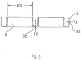
- FIG. 5 is a partial cross-sectional side view of the EMI gasket 1.
- the contact portion 35 of the EMI gasket 1 includes an inside diameter ID1 associated with port 8.
- the contact portion 35 has a thickness T1 and the remainder or body 32 of the EMI gasket 1 has a thickness T2.
- the inside diameter ID1 of the EMI gasket 1 is greater than the outside diameter OD1 of the boss 33 so that the boss 33 can enter the contact portion 35 of the EMI gasket 1.
- the inside diameter ID1 is less than the outside diameter OD2 of boss 33.
- the boss 33 when the boss 33 is further introduced into the contact portion 35, the outside diameter of the boss 33 engages the contact portion 35, and when the boss 33 and hence the ganged connector 30 are further urged toward the printed circuit board 3 so that the boss 33 contacts the surface 34 of the printed circuit board 3, then a portion of the contact portion 35 is deformed to a larger diameter. Preferably the deformation is elastic.
- the boss 33 is substantially rigid. When the boss 33 contacts the contact portion 35, then the ganged connector 30 is in electrical communication with the EMI gasket 1, and thus the components are grounded to each other. Thickness Ti is shown as being substantially the same as thickness T2.
- thickness T1 need not be substantially the same as T2.
- dimension B which identifies the height of the EMI gasket 1 can be substantially different than as shown in Figure 2 . If the deformation is elastic, then the gang connector 30 can be mounted and de-mounted to the EMI gasket 1 more than once. Additionally, it has been found that adequate isolation can be achieved even if the boss 33 does not contact the surface 34 of the printed circuit board 3, but it must be close. However, it is preferable that the boss 33 does contact the surface 34 of the printed circuit board 3.
- FIG. 6 is a perspective view of a second embodiment of the invention which is an EMI gasket 10 having a contact portion 11 which includes slots 37 in the contact portion 11. Otherwise, EMI gasket 10 is substantially similar to EMI gasket 1.
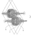
- Figure 7 is a partial perspective view of the contact portion 11, including the slots 37, of EMI gasket 10 engaged with boss 33.
- the slotted contact portion 11 allows for more flexibility of the contact portion 11 as compared to the contact portion 35 that does not include slots, yet the EMI gasket 10 still provides for adequate reduction of electromagnetic interference between adjacent ports of the ganged connector 30.
- FIG 8 is a perspective view of a third embodiment of the invention which is an EMI gasket 20 having a contact portion 39 which includes triangular-shaped sections 21. Otherwise, EMI gasket 20 is substantially similar to EMI gasket 1.
- Figure 9 is a partial perspective view of the contact portion 39, including the triangular-shaped sections 21, of EMI gasket 20 engaged with boss 33.
- the contact portion 39, including the triangular-shaped sections 21, allows for more flexibility of the contact portion 39 as compared to the contact portion 35 that does not include triangular-shaped sections, yet the EMI gasket 20 still provides for adequate reduction of electromagnetic interference between adjacent ports of the ganged connector 30.
Landscapes
- Engineering & Computer Science (AREA)
- Microelectronics & Electronic Packaging (AREA)
- Physics & Mathematics (AREA)
- Electromagnetism (AREA)
- Shielding Devices Or Components To Electric Or Magnetic Fields (AREA)
- Coupling Device And Connection With Printed Circuit (AREA)
Description
- The invention concerns an EMI gasket which is mountable to a printed circuit board (PCB) and which is also engageable with a connector which reduces electromagnetic interference (EMI).
- Devices such as a gasket which is made of an elastomeric material which is impregnated with conductive material are known. Also, electrical connectors which operate in the RF spectrum are known. Typically, the gasket is mounted between the printed circuit board and the electrical connector so as to reduce the amount of electromagnetic radiation which potentially could escape somewhere between the surface of the PCB and the electrical connector. As the number of transmitted electrical signals increases the number of electrical connectors increases. However, in some applications, the amount of space available to accommodate the electrical connectors has not increased. Thus, the density per unit space of connectors is increased. The density can be increased, but the increase in density is limited by how closely the port of one coaxial conductor can be placed adjacent to the port of another coaxial conductor without there being an unacceptable amount of crosstalk or leakage of electromagnetic radiation from one port to another port. The amount of leakage becomes unacceptable when the signal being transported by one of the coaxial conductors is corrupted by the electromagnetic radiation emitted by the other coaxial conductor.
- Also known in the art are ganged connectors, such as the connector disclosed in
U.S. Patent No. 7,927,125 . This connector has a predefined number of electrical ports that can be accommodated. If the number of desired ports exceeds the number of ports provided on the connector, then another connector must be used or a special connector must be made.JP 2006100521A - The invention relates to an EMI gasket according to
claim 1, said gasket being mountable to a printed circuit board and engageable with a ganged connector which reduces the amount of electromagnetic radiation emitted between ports of the ganged electrical connector when the ganged electrical connector is connected to a printed circuit board. - According to the invention, there is provided an EMI gasket mountable to a printed circuit board and engageable with a ganged connector, the printed circuit board having a surface and the ganged connector having a boss with a tapered outer wall, the gasket comprising a body and a plurality of ports comprising a plurality of contact portions in electrical association with the body, the contact portions each having an inner wall defining an inside diameter (ID1), the body and the contact portions including a conductive material,
characterised in that the body is a planar body, the planar body being configured and dimensioned such that when the planar body is mounted on the printed circuit board no air pockets are formed or exist between the planar body and the printed circuit board, the inner wall of one of the ports is configured to contact the tapered outer wall of the boss when the ganged connector is introduced toward the printed circuit board so that the gasket is in electrical communication with the boss and an amount of electromagnetic radiation emitted between ports is reduced when the ganged connector is connected to the printed circuit board, the contact portions having an annular shape extending from the planar body so that a portion of each contact portion is deformable, when the ganged connector is urged toward the printed circuit board. - In certain embodiments, each contact portion may include at least one slot.
- In certain embodiments, each contact portion may include at least one triangular-shaped section.
- Each contact portion has an inside diameter (ID1) and an overall thickness (T1), and the body has an overall thickness (T2).
- In certain embodiments, the overall thickness (T2) of the body may be greater than the overall thickness (T1) of each contact portion.
- In another aspect of the present disclosure, an EMI gasket is disclosed that includes a planar body having an overall thickness (T2), and a plurality of contact portions in electrical association with the body so as to form ports, wherein each contact portion has an overall thickness (T1).
- The body and the plurality of contact portions include a conductive material, e.g., aluminium, beryllium copper, or combinations thereof.
- In certain embodiments, the overall thickness (T2) of the body may be greater than the overall thickness (T1) of each contact portion, whereas in certain other embodiments, the overall thickness (T2) of the body may be equal to the overall thickness (T1) of each contact portion.
- The disclosed gasket includes a planar body, and a plurality of contact portions in electrical association with the body so as to form ports, wherein each contact portion has an inner wall defining an inside diameter (ID1).
- The body and plurality of contact portions include a conductive material, e.g., aluminium, beryllium copper, or combinations thereof.
- The gasket is configured and dimensioned such that, when mounted on the printed circuit board, no air pockets are formed or exist between the gasket and the printed circuit board.
- The ganged connector is configured and dimensioned such that when the ganged connector is introduced toward the printed circuit board, the at least one boss of the ganged connector is introduced into contact with one of the plurality of contact portions. The ganged connector is further configured and dimensioned such that when the ganged connector is introduced into contact with the printed circuit board, the tapered outer wall of the boss contacts the inner wall of one of the ports so that the boss is in electrical communication with the gasket.
- The gasket has a height which is less than a distance measured between the surface of the printed circuit board and a surface on the ganged connector from which the boss originates.
- In certain embodiments, each contact portion may include at least one slot.
- In certain embodiments, each contact portion may include at least one triangular-shaped section.
- A more complete appreciation of the invention and many of the attendant advantages thereof will be readily obtained as the same becomes better understood by reference to the following detailed description when considered in connection with the accompanying drawings, wherein:
-
Figure 1 is a perspective view of a first embodiment of the gasket of the invention; -
Figure 2 is a partial cross-sectional side view of the gasket ofFigure 1 , taken along section line 2-2, mounted between a ganged connector and a printed circuit board; -
Figure 3 is the partial cross-sectional side view ofFigure 2 , minus the conductors and insulative spacers, which identifies more details of the gasket ofFigure 1 ; -
Figure 4 is a partial cross-sectional side view of the ganged connector ofFigure 2 ; -
Figure 5 is a partial cross-sectional side view of the gasket of the invention as taken fromFigure 2 ; -
Figure 6 is a perspective view of a second embodiment of the invention; -
Figure 7 is a partial perspective view of the second embodiment of the invention as it engages the ganged connector; -
Figure 8 is a perspective view of a third embodiment of the invention; and -
Figure 9 is a partial perspective view of the third embodiment of the invention as it engages the ganged connector. - Referring now to the drawings, wherein like reference numerals designate identical or corresponding parts through the several views, embodiments of the present invention are displayed therein.
-
Figure 1 is a perspective view of the first embodiment of theEMI gasket 1. TheEMI gasket 1 contains forty-eight ports which are arranged in two rows where each row contains twenty-four ports. Afirst port 8 and a second port 9 are identified. TheEMI gasket 1 is constructed of a conductive metallic material such as aluminium or beryllium copper. TheEMI gasket 1 includes acontact portion 35 which is shown in conjunction withport 8, but note that each port includes a contact portion. Thecontact portion 35 can be machined integral with the remainder of theEMI gasket 1 or thecontact portions 35 can be joined to the remainder of the EMI gasket by way of welding, brazing, or other joining techniques well known in the art. Thecontact portion 35 is shown to have a shape of a ring or annulus. -
Figure 2 is a partial cross-sectional side view of the first embodiment of the invention, taken along section line 2-2 ofFigure 1 , where theEMI gasket 1 is soldered to a printedcircuit board 3. TheEMI gasket 1 is soldered to the printedcircuit board 3 so that no air pockets are formed or exist between theEMI gasket 1 and the printedcircuit board 3. TheEMI gasket 1 is also shown engaged with a gangedconnector 30. Further shown are a conductor 6 positioned inport 8, where the conductor 6 is separated from the conductive body of the gangedconnector 30 by aninsulative spacer 7. Still further shown are aconductor 4 positioned in port 9, where theconductor 4 is separated from the conductive body of the gangedconnector 30 by aninsulative spacer 5. The engagement of the EMI gasket 1 with the printedcircuit board 3 and with the gangedconnector 30 prevents an unacceptable level of electromagnetic radiation from entering one port from another port. Thus the signals being carried byconductors 4 and 6 are not corrupted. For reasons of clarity, theEMI gasket 1 is not shown as being cross-hatched, even though the component is section, since theEMI gasket 1 is relatively thin as compared to the other components. -
Figure 3 is the partial cross-sectional side view ofFigure 2 withoutconductors 4, 6 andinsulative spacers boss 33 is shown as projecting from the body of the gangedconnector 30. Theboss 33 generally has a ring or annular shape. Theboss 33 of the gangedconnector 30 is shown in contact with asurface 34 of the printedcircuit board 3. A boss is associated with each port. The outside diameter of theboss 33 is shown to have a draft angle C. A distance A identifies the distance from thesurface 34 of the printedcircuit board 3 to a surface from which theboss 33 originates out of the body of the gangedconnector 30 when theboss 33 contacts thesurface 34 of the printedcircuit board 3. A distance B identifies a height of theEMI gasket 1. Note that distance A is greater than distance B. -
Figure 4 is a partial cross-sectional side view of the gangedconnector 30 includingboss 33. Identified inFigure 4 are an outside diameter OD1 of theboss 33 and an outside diameter OD2 of theboss 33 which are associated withport 8. Note that outside diameter OD2 is greater than outside diameter OD1. -
Figure 5 is a partial cross-sectional side view of theEMI gasket 1. Thecontact portion 35 of theEMI gasket 1 includes an inside diameter ID1 associated withport 8. Thecontact portion 35 has a thickness T1 and the remainder orbody 32 of theEMI gasket 1 has a thickness T2. The inside diameter ID1 of theEMI gasket 1 is greater than the outside diameter OD1 of theboss 33 so that theboss 33 can enter thecontact portion 35 of theEMI gasket 1. The inside diameter ID1 is less than the outside diameter OD2 ofboss 33. So, when theboss 33 is further introduced into thecontact portion 35, the outside diameter of theboss 33 engages thecontact portion 35, and when theboss 33 and hence the gangedconnector 30 are further urged toward the printedcircuit board 3 so that theboss 33 contacts thesurface 34 of the printedcircuit board 3, then a portion of thecontact portion 35 is deformed to a larger diameter. Preferably the deformation is elastic. As compared to thecontact portion 35, theboss 33 is substantially rigid. When theboss 33 contacts thecontact portion 35, then the gangedconnector 30 is in electrical communication with theEMI gasket 1, and thus the components are grounded to each other. Thickness Ti is shown as being substantially the same as thickness T2. - However, note that thickness T1 need not be substantially the same as T2. Additionally, dimension B which identifies the height of the
EMI gasket 1 can be substantially different than as shown inFigure 2 . If the deformation is elastic, then thegang connector 30 can be mounted and de-mounted to theEMI gasket 1 more than once. Additionally, it has been found that adequate isolation can be achieved even if theboss 33 does not contact thesurface 34 of the printedcircuit board 3, but it must be close. However, it is preferable that theboss 33 does contact thesurface 34 of the printedcircuit board 3. -
Figure 6 is a perspective view of a second embodiment of the invention which is anEMI gasket 10 having acontact portion 11 which includesslots 37 in thecontact portion 11. Otherwise,EMI gasket 10 is substantially similar toEMI gasket 1. -
Figure 7 is a partial perspective view of thecontact portion 11, including theslots 37, ofEMI gasket 10 engaged withboss 33. The slottedcontact portion 11 allows for more flexibility of thecontact portion 11 as compared to thecontact portion 35 that does not include slots, yet theEMI gasket 10 still provides for adequate reduction of electromagnetic interference between adjacent ports of the gangedconnector 30. -
Figure 8 is a perspective view of a third embodiment of the invention which is anEMI gasket 20 having acontact portion 39 which includes triangular-shapedsections 21. Otherwise,EMI gasket 20 is substantially similar toEMI gasket 1. -
Figure 9 is a partial perspective view of thecontact portion 39, including the triangular-shapedsections 21, ofEMI gasket 20 engaged withboss 33. Thecontact portion 39, including the triangular-shapedsections 21, allows for more flexibility of thecontact portion 39 as compared to thecontact portion 35 that does not include triangular-shaped sections, yet theEMI gasket 20 still provides for adequate reduction of electromagnetic interference between adjacent ports of the gangedconnector 30.
Claims (5)
- An EMI gasket (20) mountable to a printed circuit board (3) and engageable with a ganged connector (30), the printed circuit board (3) having a surface (34) and the ganged connector (30) having a boss (33) with a tapered outer wall, the gasket (20) comprising a body and a plurality of ports (8, 9) comprising a plurality of contact portions (35, 39) in electrical association with the body, the contact portions (35, 39) each having an inner wall defining an inside diameter (ID1), the body and the contact portions (35, 39) including a conductive material,
characterised in that the body is a planar body, the planar body being configured and dimensioned such that when the planar body is mounted on the printed circuit board (3) no air pockets are formed or exist between the planar body and the printed circuit board (3), the inner wall of one of the ports (8, 9) is configured to contact the tapered outer wall of the boss (33) when the ganged connector (30) is introduced toward the printed circuit board (3) so that the gasket (20) is in electrical communication with the boss (33) and an amount of electromagnetic radiation emitted between ports is reduced when the ganged connector (30) is connected to the printed circuit board (3), the contact portions (35, 39) having an annular shape extending from the planar body so that a portion of each contact portion (35, 39) is deformable, when the ganged connector (30) is urged toward the printed circuit board (3). - The EMI gasket according to claim 1, wherein the body and the contact portions (35, 39) include aluminium.
- The EMI gasket according to claim 1, wherein the body and the contact portions (35, 39) include beryllium copper.
- The EMI gasket according to any one of claims 1 to 3, wherein each of the contact portions (35, 39) includes at least one slot (37).
- The EMI gasket according to any one of claims 1 to 3, wherein each of the contact portions (35, 39) includes a triangular-shaped section (21) that extends in a direction away from the planar body.
Applications Claiming Priority (2)
| Application Number | Priority Date | Filing Date | Title |
|---|---|---|---|
| US201461966482P | 2014-02-23 | 2014-02-23 | |
| PCT/US2015/016807 WO2015127196A1 (en) | 2014-02-23 | 2015-02-20 | High isolation grounding device |
Publications (3)
| Publication Number | Publication Date |
|---|---|
| EP3108543A1 EP3108543A1 (en) | 2016-12-28 |
| EP3108543A4 EP3108543A4 (en) | 2017-10-18 |
| EP3108543B1 true EP3108543B1 (en) | 2020-03-25 |
Family
ID=57346269
Family Applications (1)
| Application Number | Title | Priority Date | Filing Date |
|---|---|---|---|
| EP15752878.7A Active EP3108543B1 (en) | 2014-02-23 | 2015-02-20 | High isolation grounding device |
Country Status (2)
| Country | Link |
|---|---|
| EP (1) | EP3108543B1 (en) |
| CN (1) | CN106415934B (en) |
Family Cites Families (6)
| Publication number | Priority date | Publication date | Assignee | Title |
|---|---|---|---|---|
| JP3288875B2 (en) * | 1994-11-28 | 2002-06-04 | 株式会社東芝 | Mounting structure of shield case |
| US6878147B2 (en) * | 2001-11-02 | 2005-04-12 | Vivant Medical, Inc. | High-strength microwave antenna assemblies |
| JP4246682B2 (en) * | 2004-09-29 | 2009-04-02 | 北川工業株式会社 | Electromagnetic shielding gasket |
| US7511230B2 (en) * | 2004-11-09 | 2009-03-31 | Stealthdrive, Inc. | Reduced cost and gasketting “one-hit” and other manufacturing EMI-shielding solutions for computer enclosures |
| US20100124854A1 (en) * | 2008-11-17 | 2010-05-20 | Liu Ting-Pan | Structure for improving the voltage difference of a connector |
| US7934954B1 (en) * | 2010-04-02 | 2011-05-03 | John Mezzalingua Associates, Inc. | Coaxial cable compression connectors |
-
2015
- 2015-02-20 EP EP15752878.7A patent/EP3108543B1/en active Active
- 2015-02-20 CN CN201580020708.6A patent/CN106415934B/en active Active
Non-Patent Citations (1)
| Title |
|---|
| None * |
Also Published As
| Publication number | Publication date |
|---|---|
| EP3108543A4 (en) | 2017-10-18 |
| EP3108543A1 (en) | 2016-12-28 |
| CN106415934B (en) | 2019-04-09 |
| CN106415934A (en) | 2017-02-15 |
Similar Documents
| Publication | Publication Date | Title |
|---|---|---|
| US9510489B2 (en) | High isolation grounding device | |
| EP3761454B1 (en) | Plug and socket connectors | |
| JP6840840B2 (en) | Shielded board-to-board connector | |
| US10498055B2 (en) | Board to board connector assembly | |
| US9425564B2 (en) | Connector | |
| US8840432B2 (en) | Circuit board and wire assembly | |
| JP6705629B2 (en) | Connector assembly including conductive holder member | |
| EP2946444B1 (en) | Electrical connector system with backplane connector and daughtercard connector | |
| US8672710B2 (en) | Gasket with fingers for RJ45 cable connector | |
| US10454223B2 (en) | Connector assembly and related methods and assemblies | |
| US10566740B2 (en) | Shielding structure for a contact module of an electrical connector | |
| US9490586B1 (en) | Electrical connector having a ground shield | |
| US20100285675A1 (en) | Electrical connector assembly having connectors mounted to a circuit board | |
| CN101437361A (en) | Printed circuit board assembly | |
| US4381129A (en) | Grounded, multi-pin connector for shielded flat cable | |
| US20170059798A1 (en) | Emi shield to suppress emi leakage from one or more optical ports of an optical communications module | |
| US9502826B1 (en) | Electrical connector assembly having a plug with a first shielding housing and a socket with a second shielding housing | |
| US9240656B1 (en) | Connector assembly with cable bundle | |
| EP3108543A1 (en) | High isolation grounding device | |
| EP3621162B1 (en) | Electrical connector with non-uniformly arranged contacts | |
| US9426880B2 (en) | Noise suppression assembly and electronic device having the same | |
| US20260121311A1 (en) | Rf plug connector, rf receptacle connector, and rf connector | |
| US9461383B1 (en) | High signal isolation electrical connector | |
| US9543716B2 (en) | Electrically compensated SMA shell connector with cable dielectric captivation | |
| JP2010027290A (en) | High-frequency circuit unit |
Legal Events
| Date | Code | Title | Description |
|---|---|---|---|
| PUAI | Public reference made under article 153(3) epc to a published international application that has entered the european phase |
Free format text: ORIGINAL CODE: 0009012 |
|
| STAA | Information on the status of an ep patent application or granted ep patent |
Free format text: STATUS: REQUEST FOR EXAMINATION WAS MADE |
|
| 17P | Request for examination filed |
Effective date: 20160819 |
|
| AK | Designated contracting states |
Kind code of ref document: A1 Designated state(s): AL AT BE BG CH CY CZ DE DK EE ES FI FR GB GR HR HU IE IS IT LI LT LU LV MC MK MT NL NO PL PT RO RS SE SI SK SM TR |
|
| AX | Request for extension of the european patent |
Extension state: BA ME |
|
| DAX | Request for extension of the european patent (deleted) | ||
| A4 | Supplementary search report drawn up and despatched |
Effective date: 20170915 |
|
| RIC1 | Information provided on ipc code assigned before grant |
Ipc: H01R 13/6594 20110101ALI20170911BHEP Ipc: H01R 13/03 20060101AFI20170911BHEP Ipc: H01R 24/50 20110101ALI20170911BHEP Ipc: H01R 13/6598 20110101ALI20170911BHEP Ipc: H05K 9/00 20060101ALI20170911BHEP Ipc: H01R 103/00 20060101ALN20170911BHEP |
|
| STAA | Information on the status of an ep patent application or granted ep patent |
Free format text: STATUS: EXAMINATION IS IN PROGRESS |
|
| 17Q | First examination report despatched |
Effective date: 20190318 |
|
| RIC1 | Information provided on ipc code assigned before grant |
Ipc: H01R 13/6598 20110101ALI20190705BHEP Ipc: H01R 13/03 20060101AFI20190705BHEP Ipc: H05K 9/00 20060101ALI20190705BHEP Ipc: H01R 103/00 20060101ALN20190705BHEP Ipc: H01R 13/6594 20110101ALI20190705BHEP Ipc: H01R 24/50 20110101ALI20190705BHEP |
|
| REG | Reference to a national code |
Ref country code: DE Ref legal event code: R079 Ref document number: 602015049412 Country of ref document: DE Free format text: PREVIOUS MAIN CLASS: H01R0004660000 Ipc: H01R0013030000 |
|
| RIC1 | Information provided on ipc code assigned before grant |
Ipc: H01R 13/03 20060101AFI20191121BHEP Ipc: H01R 13/6594 20110101ALI20191121BHEP Ipc: H01R 103/00 20060101ALN20191121BHEP Ipc: H01R 24/50 20110101ALI20191121BHEP Ipc: H01R 13/6598 20110101ALI20191121BHEP Ipc: H05K 9/00 20060101ALI20191121BHEP |
|
| RIC1 | Information provided on ipc code assigned before grant |
Ipc: H01R 24/50 20110101ALI20191126BHEP Ipc: H01R 13/6598 20110101ALI20191126BHEP Ipc: H05K 9/00 20060101ALI20191126BHEP Ipc: H01R 103/00 20060101ALN20191126BHEP Ipc: H01R 13/6594 20110101ALI20191126BHEP Ipc: H01R 13/03 20060101AFI20191126BHEP |
|
| GRAP | Despatch of communication of intention to grant a patent |
Free format text: ORIGINAL CODE: EPIDOSNIGR1 |
|
| STAA | Information on the status of an ep patent application or granted ep patent |
Free format text: STATUS: GRANT OF PATENT IS INTENDED |
|
| INTG | Intention to grant announced |
Effective date: 20200103 |
|
| GRAS | Grant fee paid |
Free format text: ORIGINAL CODE: EPIDOSNIGR3 |
|
| GRAA | (expected) grant |
Free format text: ORIGINAL CODE: 0009210 |
|
| STAA | Information on the status of an ep patent application or granted ep patent |
Free format text: STATUS: THE PATENT HAS BEEN GRANTED |
|
| AK | Designated contracting states |
Kind code of ref document: B1 Designated state(s): AL AT BE BG CH CY CZ DE DK EE ES FI FR GB GR HR HU IE IS IT LI LT LU LV MC MK MT NL NO PL PT RO RS SE SI SK SM TR |
|
| REG | Reference to a national code |
Ref country code: GB Ref legal event code: FG4D |
|
| REG | Reference to a national code |
Ref country code: AT Ref legal event code: REF Ref document number: 1249660 Country of ref document: AT Kind code of ref document: T Effective date: 20200415 Ref country code: IE Ref legal event code: FG4D |
|
| REG | Reference to a national code |
Ref country code: DE Ref legal event code: R096 Ref document number: 602015049412 Country of ref document: DE |
|
| PG25 | Lapsed in a contracting state [announced via postgrant information from national office to epo] |
Ref country code: RS Free format text: LAPSE BECAUSE OF FAILURE TO SUBMIT A TRANSLATION OF THE DESCRIPTION OR TO PAY THE FEE WITHIN THE PRESCRIBED TIME-LIMIT Effective date: 20200325 Ref country code: FI Free format text: LAPSE BECAUSE OF FAILURE TO SUBMIT A TRANSLATION OF THE DESCRIPTION OR TO PAY THE FEE WITHIN THE PRESCRIBED TIME-LIMIT Effective date: 20200325 Ref country code: NO Free format text: LAPSE BECAUSE OF FAILURE TO SUBMIT A TRANSLATION OF THE DESCRIPTION OR TO PAY THE FEE WITHIN THE PRESCRIBED TIME-LIMIT Effective date: 20200625 |
|
| PG25 | Lapsed in a contracting state [announced via postgrant information from national office to epo] |
Ref country code: LV Free format text: LAPSE BECAUSE OF FAILURE TO SUBMIT A TRANSLATION OF THE DESCRIPTION OR TO PAY THE FEE WITHIN THE PRESCRIBED TIME-LIMIT Effective date: 20200325 Ref country code: SE Free format text: LAPSE BECAUSE OF FAILURE TO SUBMIT A TRANSLATION OF THE DESCRIPTION OR TO PAY THE FEE WITHIN THE PRESCRIBED TIME-LIMIT Effective date: 20200325 Ref country code: HR Free format text: LAPSE BECAUSE OF FAILURE TO SUBMIT A TRANSLATION OF THE DESCRIPTION OR TO PAY THE FEE WITHIN THE PRESCRIBED TIME-LIMIT Effective date: 20200325 Ref country code: GR Free format text: LAPSE BECAUSE OF FAILURE TO SUBMIT A TRANSLATION OF THE DESCRIPTION OR TO PAY THE FEE WITHIN THE PRESCRIBED TIME-LIMIT Effective date: 20200626 Ref country code: BG Free format text: LAPSE BECAUSE OF FAILURE TO SUBMIT A TRANSLATION OF THE DESCRIPTION OR TO PAY THE FEE WITHIN THE PRESCRIBED TIME-LIMIT Effective date: 20200625 |
|
| REG | Reference to a national code |
Ref country code: NL Ref legal event code: MP Effective date: 20200325 |
|
| REG | Reference to a national code |
Ref country code: LT Ref legal event code: MG4D |
|
| PG25 | Lapsed in a contracting state [announced via postgrant information from national office to epo] |
Ref country code: NL Free format text: LAPSE BECAUSE OF FAILURE TO SUBMIT A TRANSLATION OF THE DESCRIPTION OR TO PAY THE FEE WITHIN THE PRESCRIBED TIME-LIMIT Effective date: 20200325 |
|
| PG25 | Lapsed in a contracting state [announced via postgrant information from national office to epo] |
Ref country code: SK Free format text: LAPSE BECAUSE OF FAILURE TO SUBMIT A TRANSLATION OF THE DESCRIPTION OR TO PAY THE FEE WITHIN THE PRESCRIBED TIME-LIMIT Effective date: 20200325 Ref country code: IS Free format text: LAPSE BECAUSE OF FAILURE TO SUBMIT A TRANSLATION OF THE DESCRIPTION OR TO PAY THE FEE WITHIN THE PRESCRIBED TIME-LIMIT Effective date: 20200725 Ref country code: SM Free format text: LAPSE BECAUSE OF FAILURE TO SUBMIT A TRANSLATION OF THE DESCRIPTION OR TO PAY THE FEE WITHIN THE PRESCRIBED TIME-LIMIT Effective date: 20200325 Ref country code: RO Free format text: LAPSE BECAUSE OF FAILURE TO SUBMIT A TRANSLATION OF THE DESCRIPTION OR TO PAY THE FEE WITHIN THE PRESCRIBED TIME-LIMIT Effective date: 20200325 Ref country code: EE Free format text: LAPSE BECAUSE OF FAILURE TO SUBMIT A TRANSLATION OF THE DESCRIPTION OR TO PAY THE FEE WITHIN THE PRESCRIBED TIME-LIMIT Effective date: 20200325 Ref country code: LT Free format text: LAPSE BECAUSE OF FAILURE TO SUBMIT A TRANSLATION OF THE DESCRIPTION OR TO PAY THE FEE WITHIN THE PRESCRIBED TIME-LIMIT Effective date: 20200325 Ref country code: CZ Free format text: LAPSE BECAUSE OF FAILURE TO SUBMIT A TRANSLATION OF THE DESCRIPTION OR TO PAY THE FEE WITHIN THE PRESCRIBED TIME-LIMIT Effective date: 20200325 Ref country code: PT Free format text: LAPSE BECAUSE OF FAILURE TO SUBMIT A TRANSLATION OF THE DESCRIPTION OR TO PAY THE FEE WITHIN THE PRESCRIBED TIME-LIMIT Effective date: 20200818 |
|
| REG | Reference to a national code |
Ref country code: AT Ref legal event code: MK05 Ref document number: 1249660 Country of ref document: AT Kind code of ref document: T Effective date: 20200325 |
|
| REG | Reference to a national code |
Ref country code: DE Ref legal event code: R097 Ref document number: 602015049412 Country of ref document: DE |
|
| PG25 | Lapsed in a contracting state [announced via postgrant information from national office to epo] |
Ref country code: DK Free format text: LAPSE BECAUSE OF FAILURE TO SUBMIT A TRANSLATION OF THE DESCRIPTION OR TO PAY THE FEE WITHIN THE PRESCRIBED TIME-LIMIT Effective date: 20200325 Ref country code: AT Free format text: LAPSE BECAUSE OF FAILURE TO SUBMIT A TRANSLATION OF THE DESCRIPTION OR TO PAY THE FEE WITHIN THE PRESCRIBED TIME-LIMIT Effective date: 20200325 Ref country code: ES Free format text: LAPSE BECAUSE OF FAILURE TO SUBMIT A TRANSLATION OF THE DESCRIPTION OR TO PAY THE FEE WITHIN THE PRESCRIBED TIME-LIMIT Effective date: 20200325 Ref country code: IT Free format text: LAPSE BECAUSE OF FAILURE TO SUBMIT A TRANSLATION OF THE DESCRIPTION OR TO PAY THE FEE WITHIN THE PRESCRIBED TIME-LIMIT Effective date: 20200325 |
|
| PLBE | No opposition filed within time limit |
Free format text: ORIGINAL CODE: 0009261 |
|
| STAA | Information on the status of an ep patent application or granted ep patent |
Free format text: STATUS: NO OPPOSITION FILED WITHIN TIME LIMIT |
|
| PG25 | Lapsed in a contracting state [announced via postgrant information from national office to epo] |
Ref country code: PL Free format text: LAPSE BECAUSE OF FAILURE TO SUBMIT A TRANSLATION OF THE DESCRIPTION OR TO PAY THE FEE WITHIN THE PRESCRIBED TIME-LIMIT Effective date: 20200325 |
|
| 26N | No opposition filed |
Effective date: 20210112 |
|
| PG25 | Lapsed in a contracting state [announced via postgrant information from national office to epo] |
Ref country code: SI Free format text: LAPSE BECAUSE OF FAILURE TO SUBMIT A TRANSLATION OF THE DESCRIPTION OR TO PAY THE FEE WITHIN THE PRESCRIBED TIME-LIMIT Effective date: 20200325 |
|
| PG25 | Lapsed in a contracting state [announced via postgrant information from national office to epo] |
Ref country code: MC Free format text: LAPSE BECAUSE OF FAILURE TO SUBMIT A TRANSLATION OF THE DESCRIPTION OR TO PAY THE FEE WITHIN THE PRESCRIBED TIME-LIMIT Effective date: 20200325 |
|
| REG | Reference to a national code |
Ref country code: BE Ref legal event code: MM Effective date: 20210228 |
|
| PG25 | Lapsed in a contracting state [announced via postgrant information from national office to epo] |
Ref country code: CH Free format text: LAPSE BECAUSE OF NON-PAYMENT OF DUE FEES Effective date: 20210228 Ref country code: LI Free format text: LAPSE BECAUSE OF NON-PAYMENT OF DUE FEES Effective date: 20210228 Ref country code: LU Free format text: LAPSE BECAUSE OF NON-PAYMENT OF DUE FEES Effective date: 20210220 |
|
| PG25 | Lapsed in a contracting state [announced via postgrant information from national office to epo] |
Ref country code: IE Free format text: LAPSE BECAUSE OF NON-PAYMENT OF DUE FEES Effective date: 20210220 |
|
| PG25 | Lapsed in a contracting state [announced via postgrant information from national office to epo] |
Ref country code: BE Free format text: LAPSE BECAUSE OF NON-PAYMENT OF DUE FEES Effective date: 20210228 |
|
| PG25 | Lapsed in a contracting state [announced via postgrant information from national office to epo] |
Ref country code: HU Free format text: LAPSE BECAUSE OF FAILURE TO SUBMIT A TRANSLATION OF THE DESCRIPTION OR TO PAY THE FEE WITHIN THE PRESCRIBED TIME-LIMIT; INVALID AB INITIO Effective date: 20150220 |
|
| PG25 | Lapsed in a contracting state [announced via postgrant information from national office to epo] |
Ref country code: CY Free format text: LAPSE BECAUSE OF FAILURE TO SUBMIT A TRANSLATION OF THE DESCRIPTION OR TO PAY THE FEE WITHIN THE PRESCRIBED TIME-LIMIT Effective date: 20200325 |
|
| REG | Reference to a national code |
Ref country code: DE Ref legal event code: R082 Ref document number: 602015049412 Country of ref document: DE Representative=s name: KRAUS & LEDERER PARTGMBB, DE |
|
| PG25 | Lapsed in a contracting state [announced via postgrant information from national office to epo] |
Ref country code: MK Free format text: LAPSE BECAUSE OF FAILURE TO SUBMIT A TRANSLATION OF THE DESCRIPTION OR TO PAY THE FEE WITHIN THE PRESCRIBED TIME-LIMIT Effective date: 20200325 |
|
| PG25 | Lapsed in a contracting state [announced via postgrant information from national office to epo] |
Ref country code: MT Free format text: LAPSE BECAUSE OF FAILURE TO SUBMIT A TRANSLATION OF THE DESCRIPTION OR TO PAY THE FEE WITHIN THE PRESCRIBED TIME-LIMIT Effective date: 20200325 |
|
| PG25 | Lapsed in a contracting state [announced via postgrant information from national office to epo] |
Ref country code: TR Free format text: LAPSE BECAUSE OF FAILURE TO SUBMIT A TRANSLATION OF THE DESCRIPTION OR TO PAY THE FEE WITHIN THE PRESCRIBED TIME-LIMIT Effective date: 20200325 |
|
| PGFP | Annual fee paid to national office [announced via postgrant information from national office to epo] |
Ref country code: FR Payment date: 20251208 Year of fee payment: 12 |
|
| PGFP | Annual fee paid to national office [announced via postgrant information from national office to epo] |
Ref country code: GB Payment date: 20260106 Year of fee payment: 12 |
|
| PGFP | Annual fee paid to national office [announced via postgrant information from national office to epo] |
Ref country code: DE Payment date: 20251224 Year of fee payment: 12 |