EP3107117A1 - Semiconductor device and production method for semiconductor device - Google Patents
Semiconductor device and production method for semiconductor device Download PDFInfo
- Publication number
- EP3107117A1 EP3107117A1 EP14882050.9A EP14882050A EP3107117A1 EP 3107117 A1 EP3107117 A1 EP 3107117A1 EP 14882050 A EP14882050 A EP 14882050A EP 3107117 A1 EP3107117 A1 EP 3107117A1
- Authority
- EP
- European Patent Office
- Prior art keywords
- region
- depth
- density
- semiconductor substrate
- semiconductor device
- Prior art date
- Legal status (The legal status is an assumption and is not a legal conclusion. Google has not performed a legal analysis and makes no representation as to the accuracy of the status listed.)
- Granted
Links
Images



Classifications
-
- H—ELECTRICITY
- H10—SEMICONDUCTOR DEVICES; ELECTRIC SOLID-STATE DEVICES NOT OTHERWISE PROVIDED FOR
- H10D—INORGANIC ELECTRIC SEMICONDUCTOR DEVICES
- H10D84/00—Integrated devices formed in or on semiconductor substrates that comprise only semiconducting layers, e.g. on Si wafers or on GaAs-on-Si wafers
- H10D84/60—Integrated devices formed in or on semiconductor substrates that comprise only semiconducting layers, e.g. on Si wafers or on GaAs-on-Si wafers characterised by the integration of at least one component covered by groups H10D10/00 or H10D18/00, e.g. integration of BJTs
- H10D84/611—Combinations of BJTs and one or more of diodes, resistors or capacitors
- H10D84/613—Combinations of vertical BJTs and one or more of diodes, resistors or capacitors
- H10D84/617—Combinations of vertical BJTs and only diodes
-
- H—ELECTRICITY
- H10—SEMICONDUCTOR DEVICES; ELECTRIC SOLID-STATE DEVICES NOT OTHERWISE PROVIDED FOR
- H10D—INORGANIC ELECTRIC SEMICONDUCTOR DEVICES
- H10D12/00—Bipolar devices controlled by the field effect, e.g. insulated-gate bipolar transistors [IGBT]
- H10D12/01—Manufacture or treatment
- H10D12/031—Manufacture or treatment of IGBTs
- H10D12/032—Manufacture or treatment of IGBTs of vertical IGBTs
- H10D12/038—Manufacture or treatment of IGBTs of vertical IGBTs having a recessed gate, e.g. trench-gate IGBTs
-
- H—ELECTRICITY
- H10—SEMICONDUCTOR DEVICES; ELECTRIC SOLID-STATE DEVICES NOT OTHERWISE PROVIDED FOR
- H10D—INORGANIC ELECTRIC SEMICONDUCTOR DEVICES
- H10D12/00—Bipolar devices controlled by the field effect, e.g. insulated-gate bipolar transistors [IGBT]
- H10D12/411—Insulated-gate bipolar transistors [IGBT]
- H10D12/441—Vertical IGBTs
- H10D12/461—Vertical IGBTs having non-planar surfaces, e.g. having trenches, recesses or pillars in the surfaces of the emitter, base or collector regions
- H10D12/481—Vertical IGBTs having non-planar surfaces, e.g. having trenches, recesses or pillars in the surfaces of the emitter, base or collector regions having gate structures on slanted surfaces, on vertical surfaces, or in grooves, e.g. trench gate IGBTs
-
- H—ELECTRICITY
- H10—SEMICONDUCTOR DEVICES; ELECTRIC SOLID-STATE DEVICES NOT OTHERWISE PROVIDED FOR
- H10D—INORGANIC ELECTRIC SEMICONDUCTOR DEVICES
- H10D30/00—Field-effect transistors [FET]
- H10D30/60—Insulated-gate field-effect transistors [IGFET]
-
- H—ELECTRICITY
- H10—SEMICONDUCTOR DEVICES; ELECTRIC SOLID-STATE DEVICES NOT OTHERWISE PROVIDED FOR
- H10D—INORGANIC ELECTRIC SEMICONDUCTOR DEVICES
- H10D62/00—Semiconductor bodies, or regions thereof, of devices having potential barriers
- H10D62/10—Shapes, relative sizes or dispositions of the regions of the semiconductor bodies; Shapes of the semiconductor bodies
- H10D62/124—Shapes, relative sizes or dispositions of the regions of semiconductor bodies or of junctions between the regions
-
- H—ELECTRICITY
- H10—SEMICONDUCTOR DEVICES; ELECTRIC SOLID-STATE DEVICES NOT OTHERWISE PROVIDED FOR
- H10D—INORGANIC ELECTRIC SEMICONDUCTOR DEVICES
- H10D62/00—Semiconductor bodies, or regions thereof, of devices having potential barriers
- H10D62/10—Shapes, relative sizes or dispositions of the regions of the semiconductor bodies; Shapes of the semiconductor bodies
- H10D62/129—Cathode regions of diodes
-
- H—ELECTRICITY
- H10—SEMICONDUCTOR DEVICES; ELECTRIC SOLID-STATE DEVICES NOT OTHERWISE PROVIDED FOR
- H10D—INORGANIC ELECTRIC SEMICONDUCTOR DEVICES
- H10D62/00—Semiconductor bodies, or regions thereof, of devices having potential barriers
- H10D62/10—Shapes, relative sizes or dispositions of the regions of the semiconductor bodies; Shapes of the semiconductor bodies
- H10D62/13—Semiconductor regions connected to electrodes carrying current to be rectified, amplified or switched, e.g. source or drain regions
- H10D62/149—Source or drain regions of field-effect devices
- H10D62/151—Source or drain regions of field-effect devices of IGFETs
-
- H—ELECTRICITY
- H10—SEMICONDUCTOR DEVICES; ELECTRIC SOLID-STATE DEVICES NOT OTHERWISE PROVIDED FOR
- H10D—INORGANIC ELECTRIC SEMICONDUCTOR DEVICES
- H10D62/00—Semiconductor bodies, or regions thereof, of devices having potential barriers
- H10D62/10—Shapes, relative sizes or dispositions of the regions of the semiconductor bodies; Shapes of the semiconductor bodies
- H10D62/17—Semiconductor regions connected to electrodes not carrying current to be rectified, amplified or switched, e.g. channel regions
- H10D62/393—Body regions of DMOS transistors or IGBTs
-
- H—ELECTRICITY
- H10—SEMICONDUCTOR DEVICES; ELECTRIC SOLID-STATE DEVICES NOT OTHERWISE PROVIDED FOR
- H10D—INORGANIC ELECTRIC SEMICONDUCTOR DEVICES
- H10D62/00—Semiconductor bodies, or regions thereof, of devices having potential barriers
- H10D62/60—Impurity distributions or concentrations
-
- H—ELECTRICITY
- H10—SEMICONDUCTOR DEVICES; ELECTRIC SOLID-STATE DEVICES NOT OTHERWISE PROVIDED FOR
- H10D—INORGANIC ELECTRIC SEMICONDUCTOR DEVICES
- H10D8/00—Diodes
-
- H—ELECTRICITY
- H10—SEMICONDUCTOR DEVICES; ELECTRIC SOLID-STATE DEVICES NOT OTHERWISE PROVIDED FOR
- H10D—INORGANIC ELECTRIC SEMICONDUCTOR DEVICES
- H10D8/00—Diodes
- H10D8/50—PIN diodes
-
- H—ELECTRICITY
- H10—SEMICONDUCTOR DEVICES; ELECTRIC SOLID-STATE DEVICES NOT OTHERWISE PROVIDED FOR
- H10D—INORGANIC ELECTRIC SEMICONDUCTOR DEVICES
- H10D84/00—Integrated devices formed in or on semiconductor substrates that comprise only semiconducting layers, e.g. on Si wafers or on GaAs-on-Si wafers
- H10D84/01—Manufacture or treatment
- H10D84/0112—Integrating together multiple components covered by H10D8/00, H10D10/00 or H10D18/00, e.g. integrating multiple BJTs
-
- H—ELECTRICITY
- H10—SEMICONDUCTOR DEVICES; ELECTRIC SOLID-STATE DEVICES NOT OTHERWISE PROVIDED FOR
- H10D—INORGANIC ELECTRIC SEMICONDUCTOR DEVICES
- H10D84/00—Integrated devices formed in or on semiconductor substrates that comprise only semiconducting layers, e.g. on Si wafers or on GaAs-on-Si wafers
- H10D84/01—Manufacture or treatment
- H10D84/02—Manufacture or treatment characterised by using material-based technologies
- H10D84/03—Manufacture or treatment characterised by using material-based technologies using Group IV technology, e.g. silicon technology or silicon-carbide [SiC] technology
- H10D84/038—Manufacture or treatment characterised by using material-based technologies using Group IV technology, e.g. silicon technology or silicon-carbide [SiC] technology using silicon technology, e.g. SiGe
-
- H—ELECTRICITY
- H10—SEMICONDUCTOR DEVICES; ELECTRIC SOLID-STATE DEVICES NOT OTHERWISE PROVIDED FOR
- H10D—INORGANIC ELECTRIC SEMICONDUCTOR DEVICES
- H10D84/00—Integrated devices formed in or on semiconductor substrates that comprise only semiconducting layers, e.g. on Si wafers or on GaAs-on-Si wafers
- H10D84/80—Integrated devices formed in or on semiconductor substrates that comprise only semiconducting layers, e.g. on Si wafers or on GaAs-on-Si wafers characterised by the integration of at least one component covered by groups H10D12/00 or H10D30/00, e.g. integration of IGFETs
- H10D84/811—Combinations of field-effect devices and one or more diodes, capacitors or resistors
-
- H—ELECTRICITY
- H10—SEMICONDUCTOR DEVICES; ELECTRIC SOLID-STATE DEVICES NOT OTHERWISE PROVIDED FOR
- H10P—GENERIC PROCESSES OR APPARATUS FOR THE MANUFACTURE OR TREATMENT OF DEVICES COVERED BY CLASS H10
- H10P14/00—Formation of materials, e.g. in the shape of layers or pillars
- H10P14/20—Formation of materials, e.g. in the shape of layers or pillars of semiconductor materials
- H10P14/38—Formation of materials, e.g. in the shape of layers or pillars of semiconductor materials characterised by treatments done after the formation of the materials
- H10P14/3802—Crystallisation or recrystallisation of non-monocrystalline semiconductor materials, e.g. regrowth
- H10P14/3808—Crystallisation or recrystallisation of non-monocrystalline semiconductor materials, e.g. regrowth using laser beams
-
- H—ELECTRICITY
- H10—SEMICONDUCTOR DEVICES; ELECTRIC SOLID-STATE DEVICES NOT OTHERWISE PROVIDED FOR
- H10P—GENERIC PROCESSES OR APPARATUS FOR THE MANUFACTURE OR TREATMENT OF DEVICES COVERED BY CLASS H10
- H10P30/00—Ion implantation into wafers, substrates or parts of devices
- H10P30/20—Ion implantation into wafers, substrates or parts of devices into semiconductor materials, e.g. for doping
-
- H—ELECTRICITY
- H10—SEMICONDUCTOR DEVICES; ELECTRIC SOLID-STATE DEVICES NOT OTHERWISE PROVIDED FOR
- H10P—GENERIC PROCESSES OR APPARATUS FOR THE MANUFACTURE OR TREATMENT OF DEVICES COVERED BY CLASS H10
- H10P30/00—Ion implantation into wafers, substrates or parts of devices
- H10P30/20—Ion implantation into wafers, substrates or parts of devices into semiconductor materials, e.g. for doping
- H10P30/202—Ion implantation into wafers, substrates or parts of devices into semiconductor materials, e.g. for doping characterised by the semiconductor materials
- H10P30/204—Ion implantation into wafers, substrates or parts of devices into semiconductor materials, e.g. for doping characterised by the semiconductor materials into Group IV semiconductors
-
- H—ELECTRICITY
- H10—SEMICONDUCTOR DEVICES; ELECTRIC SOLID-STATE DEVICES NOT OTHERWISE PROVIDED FOR
- H10P—GENERIC PROCESSES OR APPARATUS FOR THE MANUFACTURE OR TREATMENT OF DEVICES COVERED BY CLASS H10
- H10P30/00—Ion implantation into wafers, substrates or parts of devices
- H10P30/20—Ion implantation into wafers, substrates or parts of devices into semiconductor materials, e.g. for doping
- H10P30/21—Ion implantation into wafers, substrates or parts of devices into semiconductor materials, e.g. for doping of electrically active species
-
- H—ELECTRICITY
- H10—SEMICONDUCTOR DEVICES; ELECTRIC SOLID-STATE DEVICES NOT OTHERWISE PROVIDED FOR
- H10P—GENERIC PROCESSES OR APPARATUS FOR THE MANUFACTURE OR TREATMENT OF DEVICES COVERED BY CLASS H10
- H10P30/00—Ion implantation into wafers, substrates or parts of devices
- H10P30/20—Ion implantation into wafers, substrates or parts of devices into semiconductor materials, e.g. for doping
- H10P30/28—Ion implantation into wafers, substrates or parts of devices into semiconductor materials, e.g. for doping characterised by an annealing step, e.g. for activation of dopants
-
- H—ELECTRICITY
- H10—SEMICONDUCTOR DEVICES; ELECTRIC SOLID-STATE DEVICES NOT OTHERWISE PROVIDED FOR
- H10P—GENERIC PROCESSES OR APPARATUS FOR THE MANUFACTURE OR TREATMENT OF DEVICES COVERED BY CLASS H10
- H10P95/00—Generic processes or apparatus for manufacture or treatments not covered by the other groups of this subclass
- H10P95/90—Thermal treatments, e.g. annealing or sintering
-
- H—ELECTRICITY
- H10—SEMICONDUCTOR DEVICES; ELECTRIC SOLID-STATE DEVICES NOT OTHERWISE PROVIDED FOR
- H10D—INORGANIC ELECTRIC SEMICONDUCTOR DEVICES
- H10D62/00—Semiconductor bodies, or regions thereof, of devices having potential barriers
- H10D62/10—Shapes, relative sizes or dispositions of the regions of the semiconductor bodies; Shapes of the semiconductor bodies
- H10D62/13—Semiconductor regions connected to electrodes carrying current to be rectified, amplified or switched, e.g. source or drain regions
- H10D62/137—Collector regions of BJTs
-
- H—ELECTRICITY
- H10—SEMICONDUCTOR DEVICES; ELECTRIC SOLID-STATE DEVICES NOT OTHERWISE PROVIDED FOR
- H10D—INORGANIC ELECTRIC SEMICONDUCTOR DEVICES
- H10D62/00—Semiconductor bodies, or regions thereof, of devices having potential barriers
- H10D62/10—Shapes, relative sizes or dispositions of the regions of the semiconductor bodies; Shapes of the semiconductor bodies
- H10D62/13—Semiconductor regions connected to electrodes carrying current to be rectified, amplified or switched, e.g. source or drain regions
- H10D62/141—Anode or cathode regions of thyristors; Collector or emitter regions of gated bipolar-mode devices, e.g. of IGBTs
- H10D62/148—Cathode regions of thyristors
-
- H—ELECTRICITY
- H10—SEMICONDUCTOR DEVICES; ELECTRIC SOLID-STATE DEVICES NOT OTHERWISE PROVIDED FOR
- H10D—INORGANIC ELECTRIC SEMICONDUCTOR DEVICES
- H10D8/00—Diodes
- H10D8/411—PN diodes having planar bodies
-
- H—ELECTRICITY
- H10—SEMICONDUCTOR DEVICES; ELECTRIC SOLID-STATE DEVICES NOT OTHERWISE PROVIDED FOR
- H10P—GENERIC PROCESSES OR APPARATUS FOR THE MANUFACTURE OR TREATMENT OF DEVICES COVERED BY CLASS H10
- H10P30/00—Ion implantation into wafers, substrates or parts of devices
- H10P30/20—Ion implantation into wafers, substrates or parts of devices into semiconductor materials, e.g. for doping
- H10P30/202—Ion implantation into wafers, substrates or parts of devices into semiconductor materials, e.g. for doping characterised by the semiconductor materials
-
- H—ELECTRICITY
- H10—SEMICONDUCTOR DEVICES; ELECTRIC SOLID-STATE DEVICES NOT OTHERWISE PROVIDED FOR
- H10P—GENERIC PROCESSES OR APPARATUS FOR THE MANUFACTURE OR TREATMENT OF DEVICES COVERED BY CLASS H10
- H10P34/00—Irradiation with electromagnetic or particle radiation of wafers, substrates or parts of devices
- H10P34/40—Irradiation with electromagnetic or particle radiation of wafers, substrates or parts of devices with high-energy radiation
- H10P34/42—Irradiation with electromagnetic or particle radiation of wafers, substrates or parts of devices with high-energy radiation with electromagnetic radiation, e.g. laser annealing
Definitions
- the technique disclosed herein relates to a semiconductor device.
- Patent Literature 1 discloses an RC-IGBT (Reverse Conducting Insulated Gate Bipolar Transistor) in which a diode and an IGBT are provided in a single semiconductor substrate.
- An n-type cathode layer is provided in a range exposed on a lower surface of the diode.
- An n-type buffer layer is provided above the cathode layer.
- An n-type drift layer is provided above the buffer layer.
- An n-type impurity density of the drift layer is lower than those of the buffer layer and the cathode layer.
- the n-type impurity density of the buffer layer is lower than that of the cathode layer.
- Patent Literature 1 a structure in which a high density impurity region, an intermediate density impurity region, and a low density impurity region are arranged in this order from a surface side of the substrate is widely used in a variety of semiconductor devices, such as diodes, MOSFETS, and the like.
- semiconductor devices such as diodes, MOSFETS, and the like.
- a technique that enables to further stabilize properties of a semiconductor device as aforementioned will be provided.
- the inventors of the present application study the techniques that can further increase an impurity density of the aforementioned high density impurity region.
- impurities are implanted in a vicinity of a surface of a semiconductor substrate, after which a region in the vicinity of the surface is melted, and thereafter solidified again. Since the impurities are diffused over an entirety of the melted region, the region that has again been solidified becomes a region containing the impurities at a high density. Further, when the semiconductor substrate is melted as above, crystal defects that were generated in the high-density impurity implantation can effectively be vanished. Thus, it becomes possible to form a high density impurity region having a high impurity density and a low crystal defect density.
- the n-type impurity density at the boundary between the high density impurity region and the intermediate density impurity region is required to be high.
- the n-type impurity density at the boundary is high, the high density impurity region and the intermediate density impurity region are not sufficiently separated. In this case, an inflow efficiency of electrons into the high density impurity region changes due to being influenced by both the high density impurity region and the intermediate density impurity region. Due to this, it becomes difficult to control properties of the semiconductor device.
- This description provides a semiconductor device as below.
- This semiconductor device comprises a first conductivity type region exposed on a surface of a semiconductor substrate.
- a local maximum value N1, a local minimum value N2, and a local maximum value N3 exist in a density distribution of first conductivity type impurities in the first conductivity type region measured along a thickness direction of the semiconductor substrate.
- a depth having the local maximum value N1 is located on the surface side with respect to a depth having the local minimum value N2.
- a depth having the local maximum value N3 is located on an opposite side of the surface with respect to the depth having the local minimum value N2.
- a region having a density N4 of the first conductivity type impurities is located in a part of the first conductivity type region located on an opposite side of the surface with respect to the depth having the local maximum value N3.
- a relationship of N1>N3>N2>N4 is satisfied.
- a relationship of N3/10>N2 is satisfied.
- a distance "a" from the surface to the depth having the local maximum value N1 is larger than twice a distance "b" from the depth having the local maximum value N1 to the depth having the local minimum value N2.
- the aforementioned first conductivity type impurities are of an n-type or a p-type.
- the density of the region having the density N4 does not need to be uniform, but the density N4 in the region may vary depending on positions within a range that satisfies a relationship of N2>N4.
- the distance "a" from the surface of the semiconductor substrate to the depth having the local maximum value N1 is larger than twice the distance "b" from the depth having the local maximum value N1 to the depth having the local minimum N2.
- Such an impurity distribution is called a box profile, and is a distribution characteristically obtained by the aforementioned method of activating the impurities by melting the semiconductor substrate.
- the region having the local maximum value N1 corresponds to the high density region
- the region having the local maximum value N3 corresponds to the intermediate density region
- the region having the density N4 corresponds to the low density region.
- the depth having the local minimum value N2 corresponds to a boundary between the high density region and the intermediate density region.
- the local minimum value N2 is higher than the density N4. Due to this, even if impurities having a conductivity type (which is herein referred to as a second conductivity type) that is different from the first conductivity type are diffused within the depth of the local minimum value N2 in a manufacturing process for this semiconductor device (that is, upon melting the semiconductor substrate), the region at this depth less likely becomes a second conductivity type region. That is, in this semiconductor device, the second conductivity type region is less likely to be formed at the boundary between the high density region and the intermediate density region. Further, the relationship of N3/10>N2 is satisfied in the semiconductor device.
- the local minimum value N2 is at a low density at the aforementioned degree, the high density region and the intermediate density region are sufficiently separated, and the influences exerted upon each other between these regions can be suppressed. Due to this, the inflow efficiency of electrons into the high density impurity region comes to be determined by the impurity density of the high density impurity region with hardly any influence from the intermediate density impurity region.
- the formation of the second conductivity type region at the boundary can be suppressed, and the influence of the intermediate density impurity region on the inflow efficiency of electrons into the high density impurity region can be suppressed. Thus, the properties of the semiconductor device are stabilized even in the event of mass production.
- this disclosure provides a method for manufacturing a semiconductor device.
- This method comprises a first implantation for implanting first conductivity type impurities into a surface of a semiconductor substrate of a first conductivity type, heat treating the semiconductor substrate after the first implantation at a temperature at which the semiconductor substrate does not melt, a second implantation for implanting first conductivity type impurities into the surface of the semiconductor substrate at an energy lower than in the first implantation and at a density higher than in the first implantation, and melting, after the second implantation, a region located on the surface side with respect to an average position of positions at which the first conductivity type impurities stop in the first implantation and then solidifying the region.
- the orders by which the first implantation, the heat treatment, the second implantation and the melting and solidifying may be of any order.
- the first conductivity type impurities are implanted at a relatively deep position in the first implantation, and the first conductivity type impurities that were implanted in the first implantation are activated in the heat treatment. Due to this, an intermediate density region is formed. Further, in this method, the first conductivity type impurities are implanted at a relatively shallow position in the second implantation, and the first conductivity type impurities that were implanted in the second implantation are activated in the melting and solidifying. Due to this, a high density region is formed. A region where the first conductivity type impurities did not diffuse becomes a low density region. According to this manufacturing method, a semiconductor device including the high density region, the intermediate density region, and the low density region can be manufactured.
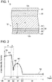
- a semiconductor device 10 of a first embodiment shown in FIG. 1 includes a semiconductor substrate 12, an anode electrode 20 provided on an upper surface 12a of the semiconductor substrate 12, and a cathode electrode 22 provided on a lower surface 12b of the semiconductor substrate 12.
- the semiconductor substrate 12 includes therein a p-type anode region 30 and an n-type cathode region 38.
- the anode region 30 is provided in a range exposed on the upper surface 12a of the semiconductor substrate 12, and is connected to the anode electrode 20.
- the cathode region 38 is provided in a range exposed on the lower surface 12b of the semiconductor substrate 12, and is connected to the cathode electrode 22. That is, a diode is provided in the semiconductor substrate 12.
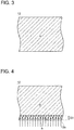
- FIG. 2 shows a density distribution of n-type impurities along a line A-A in FIG. 1 .
- a horizontal axis of FIG. 2 indicates a depth from the lower surface 12b of the semiconductor substrate 12, and a vertical axis designates an n-type impurity density in logarithmic expressions.
- the n-type impurity density rises moderately from the lower surface 12b of the semiconductor substrate 12 toward a deeper side, and comes to be of a local maximum value N1.
- the n-type impurity density steeply drops from a depth D1 having the local maximum value N1 toward the deeper side, and comes to be of a local minimum value N2.
- the n-type impurity density rises from a depth D2 having the local minimum value N2 toward the deeper side, and comes to be of a local maximum value N3.
- the n-type impurity density drops from a depth D3 having the local maximum value N3 toward the deeper side, and comes to of a density N4 at a depth D4.
- the n-type impurity density stays substantially constant at the density N4.
- the densities N1 to N4 satisfy a relationship of N1>N3>N2>N4.
- the local minimum value N2 is a value smaller than one-tenth of the local maximum value N3. That is, a relationship of N3/10>N2 is satisfied.
- an n-type impurity density Ns at the lower surface 12b of the semiconductor substrate 12 is a value greater than one-tenth of the local maximum value N1.
- the cathode region 38 located on a shallower side than the depth D2 (lower surface 12b side) will be termed a contact region 36
- the cathode region 38 between the depth D2 and the depth D4 will be termed a buffer region 34
- the cathode region 38 on the deeper side than the depth D4 (upper surface 12a side) will be termed a drift region 32.
- the depth D1 is 0.3 to 0.7 ⁇ m
- the depth D3 is 0.5 to 3.0 ⁇ m.
- the n-type impurity density varies moderately as compared to a range in the aforementioned distance "b" (range between the depth D1 and the depth D2).
- the n-type impurities are distributed in a form of a Gauss distribution.
- the buffer region 34 is a region formed by implanting the n-type impurities at the depth D3 and thereafter diffusing and activating the n-type impurities by heat treatment.
- the diode When the diode turns on (that is, when a forward voltage is applied to the diode), holes flow from the anode electrode 20 toward the cathode electrode 22, and electrons flow from the cathode electrode 22 toward the anode electrode 20.
- the contact region 36 has the high n-type impurity density, a resistance between the contact region 36 and the cathode electrode 22 is extremely low. Due to this, the electrons flow from the cathode electrode 22 into the contact region 36 with a high inflow efficiency. Further, since the crystal defect density of the contact region 36 is low, a loss is less likely to occur in the contact region when the electrons and holes pass through the contact region 36. Due to this, the diode can operate at a low loss.
- a depletion layer extends from a pn junction at a boundary between the anode region 30 and the drift region 32. Since the n-type impurity density in the buffer region 34 is relatively high, the depletion layer stops within the buffer region 34. Due to this, the depletion layer is prevented from reaching the contact region 36, as a result of which a voltage resistance of the diode is ensured.
- the buffer region 34 is provided at a relatively deep position. More specifically, the depth D3 is arranged to be located at 0.5 to 3.0 ⁇ m. Due to this, even if a scar occurs in the lower surface 12b, the scar is less likely to reach the buffer region 34. Due to this, a voltage resistance deterioration by the scar is less likely to occur.
- the n-type semiconductor substrate 12 shown in FIG. 3 is prepared.
- an entirety of the semiconductor substrate 12 has the n-type impurity density that is equal to the aforementioned density N4.
- the n-type impurities are implanted to a rear surface of the semiconductor substrate 12.
- implantation energy is adjusted so that an average position of positions at which the n-type impurities are implanted is located at the depth D3 from the lower surface 12b of the semiconductor substrate 12.
- the semiconductor substrate 12 is annealed by using a furnace or a laser annealing device.
- the anneal is performed so that the position at the depth D3 where the n-type impurities were implanted in the buffer implantation is sufficiently heated. Further, the anneal is performed at a temperature at which a surface of the semiconductor substrate 12 does not melt. Due to this, the n-type impurities that were implanted in the buffer implantation are diffused and activated. Due to this, the buffer region 34 is formed in the semiconductor substrate 12 as shown in FIG. 5 . That is, the buffer region 34 in which the n-type impurities are distributed in the Gauss distribution form as shown in FIG. 2 is formed by performing the buffer anneal.
- the local maximum value N3 of the n-type impurity density is generated after the buffer anneal in the depth D3 as shown in FIG. 2 . Further, the region on the upper surface 12a side than the buffer region 34 having the low n-type impurity density becomes the drift region 32.
- the n-type impurities are implanted to the lower surface 12b of the semiconductor substrate 12.
- the implantation energy is adjusted so that the average position of the positions at which the n-type impurities are implanted is located at a position shallower than the buffer region 34.
- the n-type impurities are implanted with a higher density than in the buffer implantation. Due to this, a region that had received the implantation of the n-type impurities in the contact implantation (that is, a region in a vicinity of the lower surface 12b) comes to have highly concentrated crystal defects.
- the semiconductor substrate 12 is annealed by laser anneal.
- the vicinity of the lower surface 12b is locally annealed by irradiating laser onto the lower surface 12b of the semiconductor substrate 12.
- the laser anneal is performed within a short period of time so that not so much heat is transmitted to the buffer region 34.
- the laser anneal is performed so that a temperature thereof rises to a level by which the semiconductor layer in the vicinity of the lower surface 12b is melted. More specifically, the laser anneal is performed so that a region on the deeper side (upper surface 12a side) than the depth D2 is not melted.
- the region 36 that was melted by the laser anneal is thereafter solidified, and recrystallized.
- the n-type impurities implanted in the contact implantation diffuse substantially uniformly within the region 36. Due to this, when the region 36 is recrystallized, the region 36 becomes the contact region 36, which contains the n-type impurities at high density. That is, as shown in FIG. 7 , the contact region 36 is formed in a range exposed on the lower surface 12b of the semiconductor substrate 12.
- the n-type impurities diffuse substantially uniformly within the region 36 when the region 36 is melted in the contact anneal.
- the n-type impurities are hardly diffused in regions that were not melted.
- FIG. 2 a distribution in which the n-type impurity density does not change so much in the region between the lower surface 12b and the depth D1, and the n-type impurity density steeply decreases from the depth D1 toward the depth D2 is obtained.
- the shown distances "a", "b" come to satisfy the relationship of a>2b.
- the contact region 36 having the box distribution is formed by performing the contact anneal.
- the region to be melted is limited to the region that is extremely shallow, a thickness of the contact region 36 becomes thin (depth D1 being 0.3 to 0.7 ⁇ m), so a peak density N1 in the contact region 36 becomes high. Further, in the process of melting the region 36 and thereafter solidifying it, majority of the crystal defects that were present at the high concentration in the region 36 are vanished. Due to this, the recrystallized contact region 36 has a reduced number of crystal defects. That is, by performing the contact anneal, the contact region 36 having a high n-type impurity density (more specifically, a high peak n-type impurity density N1) and a low crystal defect density is thereby formed. Notably, the contact anneal is performed so that the n-type impurity density N2 (see FIG. 2 ) satisfying the relationship of N3/10>N2>N4 is obtained after the contact anneal.
- the anode region 30 is formed by implanting p-type impurities into the upper surface 12a of the semiconductor substrate 12 and activating them. Then, the anode electrode 20 is formed on the upper surface 12a of the semiconductor substrate 12. Next, the cathode electrode 22 is formed on the lower surface 12b of the semiconductor substrate 12.
- the semiconductor device 10 as shown in FIG. 1 is completed by the above process.
- the contact region 36 having the high n-type impurity density and the low crystal defect density is formed.
- a diode with a low loss can be formed.
- the n-type impurities in the buffer region 34 are activated by an anneal (buffer anneal) that is different from the contact anneal that melts the surface. Due to this, the buffer region 34 can be formed at a deep position. Thus, the voltage resistance deterioration caused by scar and the like on the lower surface 12b can be suppressed.
- buffer anneal buffer anneal
- the contact anneal is performed so that the relationship of N2>N4 is satisfied. Due to this, the p-type region can be prevented from being formed in a vicinity of the depth D2. That is, there may be a case where p-type impurities are unintentionally adhered to the lower surface 12b of the semiconductor substrate 12 before being subjected to the contact anneal. In such a case, if the region 36 is melted in the contact anneal, the p-type impurities are diffused in the region 36.
- the p-type impurity density may exceed the n-type impurity density in the vicinity of the depth D2, as a result of which a p-type region may be formed in the vicinity of the depth D2.
- the contact anneal is performed so that the relationship of N2>N4 is satisfied (that is, the n-type impurity density N2 at the depth D2 becomes higher than the n-type impurity density N4 of the semiconductor substrate 12 being the base material).
- the region in the vicinity of the depth D2 is less likely to become a p-type region even if a trivial amount of p-type impurities is diffused in the vicinity of the depth D2.
- the p-type region is prevented from being formed in the depth D2. Due to this, when the semiconductor device 10 is mass-produced using the method of the present embodiment, the diode properties (especially, VF) are stabilized.
- the diode is formed so that the relationship of N3/10>N2 is satisfied. Due to this, the stabilization of the diode properties is achieved. That is, if the n-type impurity density N2 at the depth D1 is too high, the contact region 36 and the buffer region 34 will function as one single region, as a result of which the n-type impurity density in the contact region 36 and the n-type impurity density in the buffer region 34 start to influence each other's properties.
- the inflow efficiency of the electrons from the cathode electrode 22 to the contact region 36 would change not only by the n-type impurity density of the contact region 36 but also by the n-type impurity density of the buffer region 34. Due to this, it becomes difficult to accurately control the electron inflow efficiency, and a large variation would be generated in the electron inflow efficiency among the semiconductor devices upon the mass production. Contrary to this, in the method of the present embodiment, the satisfaction of the relationship N3/10>N2 allows greater robustness in the electron inflow efficiency with respect to the influence from the buffer region 34. Thus, according to the method of the embodiment, a variation is less likely to occur in the electron inflow efficiency of the contact regions of the respective semiconductor devices upon the mass production.
- the n-type impurity density Ns at the lower surface 12b is low as compared to the first embodiment.
- a distance "c" from the depth D5 to the depth D1 satisfies a relationship of c>2b.
- the semiconductor device of the second embodiment is manufactured in a same method as in the first embodiment.
- the contact region 36 having a relatively thick thickness by the method of melting the surface of the semiconductor substrate, there may be a case where the n-type impurity density Ns at the lower surface 12b becomes low as in the second embodiment. Even in such a case, in a typical box profile, the relationship of c>2b is satisfied. As above, in the case where the density Ns is low, the box profile can be defined by the distance "c" and the distance "b" (if the n-type impurity density Ns at the lower surface 12b satisfies Ns>N1/10 as in the first embodiment, the distance "a" between the lower surface 12b and the depth D1 simply needs to satisfy the relationship of a>2b). Even with the semiconductor device and the manufacturing method thereof of the second embodiment, substantially the same advantages as in the semiconductor device of the first embodiment can be obtained.
- the semiconductor devices of the comparative examples each have a contact region, a buffer region, a drift region, an anode region, a cathode electrode, and an anode electrode, similar to the first and second embodiments.
- the semiconductor devices of the comparative examples although impurity densities and dimensions of their regions may be different, the basic functionality of these regions are similar to the first and second embodiments.
- parts having common features as the first and second embodiments will be described using the same reference signs as in the first and second embodiments.
- the comparative examples hereinbelow were carried out by the inventors of the present application by experiments, and are not publicly known.
- FIG. 9 shows the n-type impurity density distribution in the contact region 36, the buffer region 34, and the drift region 32 in the semiconductor device of a first comparative example.
- the n-type impurities are implanted at the depth D3 in the semiconductor substrate.
- the n-type impurities are implanted in the vicinity of the lower surface 12b of the semiconductor substrate 12 (for example, the depth D1).
- the lower surface 12b of the semiconductor substrate 12 is melted by the laser anneal.
- the region extending to the depth D2 shown in FIG. 9 is melted. Due to this, the contact region 36 is formed.
- the buffer region 34 is formed by the heat from the laser anneal, so the buffer region 34 needs to be formed at a position close to the lower surface 12b (that is, the depth D3 needs to be made shallow). Due to this, the buffer region 34 cannot be formed at a deep position.
- the semiconductor device of the first comparative example is prone to deteriorating its voltage resistance when a scar is formed on the lower surface 12b. Further, since the n-type impurity density at the depth D2 is high, the contact region 36 and the buffer region 34 are not sufficiently separated. Due to this, when the semiconductor device is mass-produced in this method, the variation in the inflow efficiency of the electrons to the contact region 36 tends to occur.
- FIG. 10 shows the n-type impurity density distribution in the contact region 36, the buffer region 34, and the drift region 32 in the semiconductor device of a second comparative example.
- a manufacturing method of the semiconductor device of the second comparative example is similar to the first comparative example.
- the implanting depth D3 of the n-type impurities in the buffer region 34 is deeper than the first comparative example.
- the semiconductor substrate 12 is melted to a deeper position than in the first comparative example in order to activate the n-type impurities implanted to the depth D3, which is deeper than the first comparative example. Due to this, as shown in FIG.
- the semiconductor device of the second comparative example has the buffer region 34 formed at a deeper position than in the first comparative example, whereas on the other hand the contact region 36 comes to have a wider width, and the n-type impurity density in the contact region 36 is lowered. Due to this, in the semiconductor device of the second comparative example, there is a problem that the contact resistance of the contact region 36 with respect to the cathode electrode 22 is high. Further, in the semiconductor device of the second comparative example as well, the local minimum value N2 is high, so the contact region 36 and the buffer region 34 are not separated sufficiently.
- FIG. 11 shows the n-type impurity density distribution in the contact region 36, the buffer region 34, and the drift region 32 in the semiconductor device of a third comparative example.
- the n-type impurities are implanted to the depth D3.
- the depth D3 of the third comparative example is similar to the depth D3 of the first embodiment.
- the lower surface 12b of the semiconductor substrate 12 is melted by the laser anneal.
- the region at the depth D3 are not melted, however, the depth D1 is heated by melting up to a depth (depth Da in FIG. 11 ) in the vicinity of the depth D1.
- the impurities implanted in the depth D1 are diffused, and the buffer region 34 is thereby formed.
- the n-type impurities are implanted to a depth in the vicinity of the lower surface 12b of the semiconductor substrate 12.
- the lower surface 12b of the semiconductor substrate 12 is melted by the laser anneal. That is, only the region shallower than the depth Da is melted, and the n-type impurities are diffused in that melted region. Due to this, the contact region 36 is formed. According to the method of the third comparative example, the contact region 36 having the high n-type impurity density and the buffer region 34 formed at the deep position as shown in FIG. 11 can be facilitated.
- the p-type impurities are unintentionally adhered to the lower surface 12b of the semiconductor substrate 12, the p-type impurities are diffused in the melting region in the initial laser anneal (laser anneal to melt up to the depth Da). Due to this, as shown in FIG. 11 , there is a case where the p-type impurities are diffused in the region from the lower surface 12b to the depth Da. When this happens, the p-type impurity density may exceed the n-type impurity density at the depth D2 having the local minimum value N2 of n-type impurities.
- the p-type region may be formed between the contact region 36 and the buffer region 34.
- the p-type region may be formed between the contact region 36 and the buffer region 34, and the diode properties may not be stabilized upon the mass production.
- the buffer implantation, the buffer anneal, the contact implantation, and the contact anneal are performed in this order, however, the order by which these processes are performed may be changed. The order may be changed arbitrarily so long as the buffer anneal is performed after the buffer implantation, and the contact anneal is performed after the contact implantation.
- FIG. 12 a configuration shown in FIG. 12 may be exemplified.
- reference signs 20 to 22 and 30 to 36 correspond to the first embodiment.
- a reference sign 51 is an emitter region
- a reference sign 52 is a body region
- a reference sign 53 is a collector region
- a reference sign 55 is a gate insulating film
- a reference sign 56 is a gate electrode.
- the IGBT is configured by these constituent features 51 to 56, and the regions 32 and 34.
- the anode electrode 20 serves also as an emitter electrode of the IGBT
- the cathode electrode 22 serves also as a collector electrode of the IGBT.
- the diode had been described, however, the aforementioned technique may be applied to a contact portion between a source region and a source electrode, or to a contact portion between a drain region and a drain electrode of a FET (for example, MOSFET).
- a FET for example, MOSFET
Landscapes
- Electrodes Of Semiconductors (AREA)
- Metal-Oxide And Bipolar Metal-Oxide Semiconductor Integrated Circuits (AREA)
- Physics & Mathematics (AREA)
- Optics & Photonics (AREA)
- Electromagnetism (AREA)
Abstract
Description
- (Cross Reference to Related Application) This application is a related application of
Japanese Patent Application No. 2014-023873 filed on February 10, 2014 - The technique disclosed herein relates to a semiconductor device.
-
Japanese Patent Application Publication No. 2011-82220 - As in Patent Literature 1, a structure in which a high density impurity region, an intermediate density impurity region, and a low density impurity region are arranged in this order from a surface side of the substrate is widely used in a variety of semiconductor devices, such as diodes, MOSFETS, and the like. In this disclosure, a technique that enables to further stabilize properties of a semiconductor device as aforementioned will be provided.
- The inventors of the present application study the techniques that can further increase an impurity density of the aforementioned high density impurity region. In this technique, impurities are implanted in a vicinity of a surface of a semiconductor substrate, after which a region in the vicinity of the surface is melted, and thereafter solidified again. Since the impurities are diffused over an entirety of the melted region, the region that has again been solidified becomes a region containing the impurities at a high density. Further, when the semiconductor substrate is melted as above, crystal defects that were generated in the high-density impurity implantation can effectively be vanished. Thus, it becomes possible to form a high density impurity region having a high impurity density and a low crystal defect density. However, in a technique that melts the surface of the semiconductor substrate as above, a phenomenon that impurities that had been adhering to the surface of the semiconductor substrate prior to the melting diffuses into the melted region is starting to gain recognition. For example, upon forming an n-type high density impurity region, there are cases where p-type impurities had been adhering to the surface of the semiconductor substrate diffuses within the melted region. In such cases, if the n-type impurity density is low at a boundary between the high density impurity region and the intermediate density impurity region, the p-type impurities are diffused in the aforementioned region having the low n-type impurity density, and there is a case where that region becomes a p-type region. To solve such a problem, the n-type impurity density at the boundary between the high density impurity region and the intermediate density impurity region is required to be high. However, if the n-type impurity density at the boundary is high, the high density impurity region and the intermediate density impurity region are not sufficiently separated. In this case, an inflow efficiency of electrons into the high density impurity region changes due to being influenced by both the high density impurity region and the intermediate density impurity region. Due to this, it becomes difficult to control properties of the semiconductor device.
- Therefore, this description provides a semiconductor device as below. This semiconductor device comprises a first conductivity type region exposed on a surface of a semiconductor substrate. A local maximum value N1, a local minimum value N2, and a local maximum value N3 exist in a density distribution of first conductivity type impurities in the first conductivity type region measured along a thickness direction of the semiconductor substrate. A depth having the local maximum value N1 is located on the surface side with respect to a depth having the local minimum value N2. A depth having the local maximum value N3 is located on an opposite side of the surface with respect to the depth having the local minimum value N2. A region having a density N4 of the first conductivity type impurities is located in a part of the first conductivity type region located on an opposite side of the surface with respect to the depth having the local maximum value N3. A relationship of N1>N3>N2>N4 is satisfied. A relationship of N3/10>N2 is satisfied. A distance "a" from the surface to the depth having the local maximum value N1 is larger than twice a distance "b" from the depth having the local maximum value N1 to the depth having the local minimum value N2.
- Notably, the aforementioned first conductivity type impurities are of an n-type or a p-type. Further, the density of the region having the density N4 does not need to be uniform, but the density N4 in the region may vary depending on positions within a range that satisfies a relationship of N2>N4.
- In this semiconductor device, the distance "a" from the surface of the semiconductor substrate to the depth having the local maximum value N1 is larger than twice the distance "b" from the depth having the local maximum value N1 to the depth having the local minimum N2. Such an impurity distribution is called a box profile, and is a distribution characteristically obtained by the aforementioned method of activating the impurities by melting the semiconductor substrate. In this semiconductor device, the region having the local maximum value N1 corresponds to the high density region, the region having the local maximum value N3 corresponds to the intermediate density region, and the region having the density N4 corresponds to the low density region. Further, the depth having the local minimum value N2 corresponds to a boundary between the high density region and the intermediate density region. In this semiconductor device, the local minimum value N2 is higher than the density N4. Due to this, even if impurities having a conductivity type (which is herein referred to as a second conductivity type) that is different from the first conductivity type are diffused within the depth of the local minimum value N2 in a manufacturing process for this semiconductor device (that is, upon melting the semiconductor substrate), the region at this depth less likely becomes a second conductivity type region. That is, in this semiconductor device, the second conductivity type region is less likely to be formed at the boundary between the high density region and the intermediate density region. Further, the relationship of N3/10>N2 is satisfied in the semiconductor device. When the local minimum value N2 is at a low density at the aforementioned degree, the high density region and the intermediate density region are sufficiently separated, and the influences exerted upon each other between these regions can be suppressed. Due to this, the inflow efficiency of electrons into the high density impurity region comes to be determined by the impurity density of the high density impurity region with hardly any influence from the intermediate density impurity region. As above, according to this semiconductor device, the formation of the second conductivity type region at the boundary can be suppressed, and the influence of the intermediate density impurity region on the inflow efficiency of electrons into the high density impurity region can be suppressed. Thus, the properties of the semiconductor device are stabilized even in the event of mass production.
- Furthermore, this disclosure provides a method for manufacturing a semiconductor device. This method comprises a first implantation for implanting first conductivity type impurities into a surface of a semiconductor substrate of a first conductivity type, heat treating the semiconductor substrate after the first implantation at a temperature at which the semiconductor substrate does not melt, a second implantation for implanting first conductivity type impurities into the surface of the semiconductor substrate at an energy lower than in the first implantation and at a density higher than in the first implantation, and melting, after the second implantation, a region located on the surface side with respect to an average position of positions at which the first conductivity type impurities stop in the first implantation and then solidifying the region.
- Notably, so long as the heat treatment is performed after the first implantation, and the melting and solidifying are performed after the second implantation, the orders by which the first implantation, the heat treatment, the second implantation and the melting and solidifying may be of any order.
- In this method, the first conductivity type impurities are implanted at a relatively deep position in the first implantation, and the first conductivity type impurities that were implanted in the first implantation are activated in the heat treatment. Due to this, an intermediate density region is formed. Further, in this method, the first conductivity type impurities are implanted at a relatively shallow position in the second implantation, and the first conductivity type impurities that were implanted in the second implantation are activated in the melting and solidifying. Due to this, a high density region is formed. A region where the first conductivity type impurities did not diffuse becomes a low density region. According to this manufacturing method, a semiconductor device including the high density region, the intermediate density region, and the low density region can be manufactured.
-
-
FIG. 1 is a vertical cross sectional view of asemiconductor device 10 of a first embodiment; -
FIG. 2 is a graph showing an n-type impurity density along a line A-A inFIG. 1 ; -
FIG. 3 is an explanatory diagram of a manufacturing process of thesemiconductor device 10; -
FIG. 4 is an explanatory diagram of the manufacturing process of thesemiconductor device 10; -
FIG. 5 is an explanatory diagram of the manufacturing process of thesemiconductor device 10; -
FIG. 6 is an explanatory diagram of the manufacturing process of thesemiconductor device 10; -
FIG. 7 is an explanatory diagram of the manufacturing process of thesemiconductor device 10; -
FIG. 8 is a graph of a semiconductor device of a second embodiment corresponding toFIG. 2 ; -
FIG. 9 is a graph of a semiconductor device of a first comparative example corresponding toFIG. 2 ; -
FIG. 10 is a graph of a semiconductor device of a second comparative example corresponding toFIG. 2 ; -
FIG. 11 is a graph of a semiconductor device of a third comparative example corresponding toFIG. 2 ; and -
FIG. 12 is a vertical cross sectional view of an RC-IGBT that adapts the technique disclosed in this description. - Some features of embodiments described hereinbelow will be described below. Notably, the features hereinbelow are each useful independently on their own.
- (Feature 1) A depth having a density N5 of the first conductivity type impurities may be located on the surface side with respect to the depth having the local maximum value N1. The density N5 may be one tenth of the local maximum value N1. A distance "c" from the depth having the density N5 to the depth having the local maximum value N1 may be larger than twice the distance "b".
- (Feature 2) a diode and an IGBT may be provided in the semiconductor substrate, and the first conductivity type region may be a cathode region of the diode.
- (Feature 3) The depth having the local maximum value N1 may be present in a range of 0.3 to 0.7µm from a surface.
- (Feature 4) A depth having the local maximum value N3 may be present in a range of 0.5 to 3.0µm from the surface.
- (First Embodiment) A
semiconductor device 10 of a first embodiment shown inFIG. 1 includes asemiconductor substrate 12, ananode electrode 20 provided on anupper surface 12a of thesemiconductor substrate 12, and acathode electrode 22 provided on alower surface 12b of thesemiconductor substrate 12. - The
semiconductor substrate 12 includes therein a p-type anode region 30 and an n-type cathode region 38. Theanode region 30 is provided in a range exposed on theupper surface 12a of thesemiconductor substrate 12, and is connected to theanode electrode 20. Thecathode region 38 is provided in a range exposed on thelower surface 12b of thesemiconductor substrate 12, and is connected to thecathode electrode 22. That is, a diode is provided in thesemiconductor substrate 12. -
FIG. 2 shows a density distribution of n-type impurities along a line A-A inFIG. 1 . Notably, a horizontal axis ofFIG. 2 indicates a depth from thelower surface 12b of thesemiconductor substrate 12, and a vertical axis designates an n-type impurity density in logarithmic expressions. The n-type impurity density rises moderately from thelower surface 12b of thesemiconductor substrate 12 toward a deeper side, and comes to be of a local maximum value N1. The n-type impurity density steeply drops from a depth D1 having the local maximum value N1 toward the deeper side, and comes to be of a local minimum value N2. The n-type impurity density rises from a depth D2 having the local minimum value N2 toward the deeper side, and comes to be of a local maximum value N3. The n-type impurity density drops from a depth D3 having the local maximum value N3 toward the deeper side, and comes to of a density N4 at a depth D4. In a region deeper than the depth D4, the n-type impurity density stays substantially constant at the density N4. The densities N1 to N4 satisfy a relationship of N1>N3>N2>N4. Further, the local minimum value N2 is a value smaller than one-tenth of the local maximum value N3. That is, a relationship of N3/10>N2 is satisfied. Further, an n-type impurity density Ns at thelower surface 12b of thesemiconductor substrate 12 is a value greater than one-tenth of the local maximum value N1. Hereinbelow, thecathode region 38 located on a shallower side than the depth D2 (lower surface 12b side) will be termed acontact region 36, thecathode region 38 between the depth D2 and the depth D4 will be termed abuffer region 34, and thecathode region 38 on the deeper side than the depth D4 (upper surface 12a side) will be termed adrift region 32. In the present embodiment, the depth D1 is 0.3 to 0.7µm, and the depth D3 is 0.5 to 3.0µm. - A distance "a" (= D1) between the
lower surface 12b and the depth D1 is larger than twice a distance "b" (= D2-D1) between the depth D1 and the depth D2. That is, a>2b is satisfied. That is, an n-type impurity density distribution in thecontact region 36 has a box profile. That is, thecontact region 36 is formed by melting a semiconductor region to which the n-type impurities had been implanted and thereafter solidifying (recrystallizing) it. Due to this, in thecontact region 36, its crystal defect density is low despite its high n-type impurity density. - In the
buffer region 34, the n-type impurity density varies moderately as compared to a range in the aforementioned distance "b" (range between the depth D1 and the depth D2). In thebuffer region 34, the n-type impurities are distributed in a form of a Gauss distribution. Thebuffer region 34 is a region formed by implanting the n-type impurities at the depth D3 and thereafter diffusing and activating the n-type impurities by heat treatment. - When the diode turns on (that is, when a forward voltage is applied to the diode), holes flow from the
anode electrode 20 toward thecathode electrode 22, and electrons flow from thecathode electrode 22 toward theanode electrode 20. As above, since thecontact region 36 has the high n-type impurity density, a resistance between thecontact region 36 and thecathode electrode 22 is extremely low. Due to this, the electrons flow from thecathode electrode 22 into thecontact region 36 with a high inflow efficiency. Further, since the crystal defect density of thecontact region 36 is low, a loss is less likely to occur in the contact region when the electrons and holes pass through thecontact region 36. Due to this, the diode can operate at a low loss. - When the diode turns off (that is, when a reverse voltage is applied to the diode), a depletion layer extends from a pn junction at a boundary between the
anode region 30 and thedrift region 32. Since the n-type impurity density in thebuffer region 34 is relatively high, the depletion layer stops within thebuffer region 34. Due to this, the depletion layer is prevented from reaching thecontact region 36, as a result of which a voltage resistance of the diode is ensured. - Further, in a manufacturing process, if a scar occurs on the
lower surface 12b of thesemiconductor substrate 12 and if the scar reaches thebuffer region 34, the voltage resistance of the diode is deteriorated. However, in thissemiconductor device 10, thebuffer region 34 is provided at a relatively deep position. More specifically, the depth D3 is arranged to be located at 0.5 to 3.0µm. Due to this, even if a scar occurs in thelower surface 12b, the scar is less likely to reach thebuffer region 34. Due to this, a voltage resistance deterioration by the scar is less likely to occur. - Next, a manufacturing method of the
semiconductor device 10 will be described. Firstly, the n-type semiconductor substrate 12 shown inFIG. 3 is prepared. At this stage, an entirety of thesemiconductor substrate 12 has the n-type impurity density that is equal to the aforementioned density N4. - Next, as shown in
FIG. 4 , the n-type impurities are implanted to a rear surface of thesemiconductor substrate 12. Here, implantation energy is adjusted so that an average position of positions at which the n-type impurities are implanted is located at the depth D3 from thelower surface 12b of thesemiconductor substrate 12. - Next, the
semiconductor substrate 12 is annealed by using a furnace or a laser annealing device. Here, the anneal is performed so that the position at the depth D3 where the n-type impurities were implanted in the buffer implantation is sufficiently heated. Further, the anneal is performed at a temperature at which a surface of thesemiconductor substrate 12 does not melt. Due to this, the n-type impurities that were implanted in the buffer implantation are diffused and activated. Due to this, thebuffer region 34 is formed in thesemiconductor substrate 12 as shown inFIG. 5 . That is, thebuffer region 34 in which the n-type impurities are distributed in the Gauss distribution form as shown inFIG. 2 is formed by performing the buffer anneal. Since an average stop depth of the n-type impurities in the buffer implantation is the depth D3, the local maximum value N3 of the n-type impurity density is generated after the buffer anneal in the depth D3 as shown inFIG. 2 . Further, the region on theupper surface 12a side than thebuffer region 34 having the low n-type impurity density becomes thedrift region 32. - Next, as shown in
FIG. 6 , the n-type impurities are implanted to thelower surface 12b of thesemiconductor substrate 12. Here, the implantation energy is adjusted so that the average position of the positions at which the n-type impurities are implanted is located at a position shallower than thebuffer region 34. Further, in the contact implantation, the n-type impurities are implanted with a higher density than in the buffer implantation. Due to this, a region that had received the implantation of the n-type impurities in the contact implantation (that is, a region in a vicinity of thelower surface 12b) comes to have highly concentrated crystal defects. - Next, the
semiconductor substrate 12 is annealed by laser anneal. Here, the vicinity of thelower surface 12b is locally annealed by irradiating laser onto thelower surface 12b of thesemiconductor substrate 12. More specifically, the laser anneal is performed within a short period of time so that not so much heat is transmitted to thebuffer region 34. Further, the laser anneal is performed so that a temperature thereof rises to a level by which the semiconductor layer in the vicinity of thelower surface 12b is melted. More specifically, the laser anneal is performed so that a region on the deeper side (upper surface 12a side) than the depth D2 is not melted. Theregion 36 that was melted by the laser anneal is thereafter solidified, and recrystallized. The n-type impurities implanted in the contact implantation diffuse substantially uniformly within theregion 36. Due to this, when theregion 36 is recrystallized, theregion 36 becomes thecontact region 36, which contains the n-type impurities at high density. That is, as shown inFIG. 7 , thecontact region 36 is formed in a range exposed on thelower surface 12b of thesemiconductor substrate 12. - As above, the n-type impurities diffuse substantially uniformly within the
region 36 when theregion 36 is melted in the contact anneal. On the other hand, the n-type impurities are hardly diffused in regions that were not melted. As a result of this, as shown inFIG. 2 , a distribution in which the n-type impurity density does not change so much in the region between thelower surface 12b and the depth D1, and the n-type impurity density steeply decreases from the depth D1 toward the depth D2 is obtained. Thus, the shown distances "a", "b" come to satisfy the relationship of a>2b. As above, thecontact region 36 having the box distribution is formed by performing the contact anneal. Since the region to be melted is limited to the region that is extremely shallow, a thickness of thecontact region 36 becomes thin (depth D1 being 0.3 to 0.7µm), so a peak density N1 in thecontact region 36 becomes high. Further, in the process of melting theregion 36 and thereafter solidifying it, majority of the crystal defects that were present at the high concentration in theregion 36 are vanished. Due to this, the recrystallizedcontact region 36 has a reduced number of crystal defects. That is, by performing the contact anneal, thecontact region 36 having a high n-type impurity density (more specifically, a high peak n-type impurity density N1) and a low crystal defect density is thereby formed. Notably, the contact anneal is performed so that the n-type impurity density N2 (seeFIG. 2 ) satisfying the relationship of N3/10>N2>N4 is obtained after the contact anneal. - Next, the
anode region 30 is formed by implanting p-type impurities into theupper surface 12a of thesemiconductor substrate 12 and activating them. Then, theanode electrode 20 is formed on theupper surface 12a of thesemiconductor substrate 12. Next, thecathode electrode 22 is formed on thelower surface 12b of thesemiconductor substrate 12. Thesemiconductor device 10 as shown inFIG. 1 is completed by the above process. - As described above, according to the method of this embodiment, the
contact region 36 having the high n-type impurity density and the low crystal defect density is formed. Thus, a diode with a low loss can be formed. - Further, in the method of the embodiment, the n-type impurities in the
buffer region 34 are activated by an anneal (buffer anneal) that is different from the contact anneal that melts the surface. Due to this, thebuffer region 34 can be formed at a deep position. Thus, the voltage resistance deterioration caused by scar and the like on thelower surface 12b can be suppressed. - Further, in the method of the embodiment, the contact anneal is performed so that the relationship of N2>N4 is satisfied. Due to this, the p-type region can be prevented from being formed in a vicinity of the depth D2. That is, there may be a case where p-type impurities are unintentionally adhered to the
lower surface 12b of thesemiconductor substrate 12 before being subjected to the contact anneal. In such a case, if theregion 36 is melted in the contact anneal, the p-type impurities are diffused in theregion 36. Thus, if the n-type impurity density is extremely low at the depth D2, the p-type impurity density may exceed the n-type impurity density in the vicinity of the depth D2, as a result of which a p-type region may be formed in the vicinity of the depth D2. However, with the method of the present embodiment, the contact anneal is performed so that the relationship of N2>N4 is satisfied (that is, the n-type impurity density N2 at the depth D2 becomes higher than the n-type impurity density N4 of thesemiconductor substrate 12 being the base material). Due to this, the region in the vicinity of the depth D2 is less likely to become a p-type region even if a trivial amount of p-type impurities is diffused in the vicinity of the depth D2. Thus, the p-type region is prevented from being formed in the depth D2. Due to this, when thesemiconductor device 10 is mass-produced using the method of the present embodiment, the diode properties (especially, VF) are stabilized. - Further, in the method of the embodiment, the diode is formed so that the relationship of N3/10>N2 is satisfied. Due to this, the stabilization of the diode properties is achieved. That is, if the n-type impurity density N2 at the depth D1 is too high, the
contact region 36 and thebuffer region 34 will function as one single region, as a result of which the n-type impurity density in thecontact region 36 and the n-type impurity density in thebuffer region 34 start to influence each other's properties. For example, if the n-type impurity density N2 is high, the inflow efficiency of the electrons from thecathode electrode 22 to thecontact region 36 would change not only by the n-type impurity density of thecontact region 36 but also by the n-type impurity density of thebuffer region 34. Due to this, it becomes difficult to accurately control the electron inflow efficiency, and a large variation would be generated in the electron inflow efficiency among the semiconductor devices upon the mass production. Contrary to this, in the method of the present embodiment, the satisfaction of the relationship N3/10>N2 allows greater robustness in the electron inflow efficiency with respect to the influence from thebuffer region 34. Thus, according to the method of the embodiment, a variation is less likely to occur in the electron inflow efficiency of the contact regions of the respective semiconductor devices upon the mass production. - (Second Embodiment) In a semiconductor device of a second embodiment, as shown in
FIG. 8 , the n-type impurity density Ns at thelower surface 12b is low as compared to the first embodiment. In the second embodiment, N1/10>Ns is satisfied. Due to this, a depth D5 having an n-type impurity density N5, where N5=N1/10, exists in a region shallower than the depth D1. In the second embodiment, a distance "c" from the depth D5 to the depth D1 satisfies a relationship of c>2b. The semiconductor device of the second embodiment is manufactured in a same method as in the first embodiment. Upon forming thecontact region 36 having a relatively thick thickness by the method of melting the surface of the semiconductor substrate, there may be a case where the n-type impurity density Ns at thelower surface 12b becomes low as in the second embodiment. Even in such a case, in a typical box profile, the relationship of c>2b is satisfied. As above, in the case where the density Ns is low, the box profile can be defined by the distance "c" and the distance "b" (if the n-type impurity density Ns at thelower surface 12b satisfies Ns>N1/10 as in the first embodiment, the distance "a" between thelower surface 12b and the depth D1 simply needs to satisfy the relationship of a>2b). Even with the semiconductor device and the manufacturing method thereof of the second embodiment, substantially the same advantages as in the semiconductor device of the first embodiment can be obtained. - Next, semiconductor devices and manufacturing methods thereof of comparative examples will be described. Notably, the semiconductor devices of the comparative examples each have a contact region, a buffer region, a drift region, an anode region, a cathode electrode, and an anode electrode, similar to the first and second embodiments. In the semiconductor devices of the comparative examples, although impurity densities and dimensions of their regions may be different, the basic functionality of these regions are similar to the first and second embodiments. Thus, hereinbelow, parts having common features as the first and second embodiments will be described using the same reference signs as in the first and second embodiments. Further, the comparative examples hereinbelow were carried out by the inventors of the present application by experiments, and are not publicly known.
- (First Comparative Example)
FIG. 9 shows the n-type impurity density distribution in thecontact region 36, thebuffer region 34, and thedrift region 32 in the semiconductor device of a first comparative example. In a manufacturing method of the semiconductor device of the first comparative example, firstly, the n-type impurities are implanted at the depth D3 in the semiconductor substrate. Next, the n-type impurities are implanted in the vicinity of thelower surface 12b of the semiconductor substrate 12 (for example, the depth D1). Then, thelower surface 12b of thesemiconductor substrate 12 is melted by the laser anneal. At this occasion, the region extending to the depth D2 shown inFIG. 9 is melted. Due to this, thecontact region 36 is formed. Further, although the region in the vicinity of the depth D3 is not melted, it is heated by the laser anneal. Due to this, the n-type impurities are activated in the vicinity of the depth D3, and thebuffer region 34 is formed in the vicinity of the depth D3. Due to this, the semiconductor device in which the n-type impurities are distributed as shown inFIG. 9 is obtained. In the method of the first comparative example, thebuffer region 34 is formed by the heat from the laser anneal, so thebuffer region 34 needs to be formed at a position close to thelower surface 12b (that is, the depth D3 needs to be made shallow). Due to this, thebuffer region 34 cannot be formed at a deep position. Thus, the semiconductor device of the first comparative example is prone to deteriorating its voltage resistance when a scar is formed on thelower surface 12b. Further, since the n-type impurity density at the depth D2 is high, thecontact region 36 and thebuffer region 34 are not sufficiently separated. Due to this, when the semiconductor device is mass-produced in this method, the variation in the inflow efficiency of the electrons to thecontact region 36 tends to occur. - (Second Comparative Example)
FIG. 10 shows the n-type impurity density distribution in thecontact region 36, thebuffer region 34, and thedrift region 32 in the semiconductor device of a second comparative example. A manufacturing method of the semiconductor device of the second comparative example is similar to the first comparative example. However, the implanting depth D3 of the n-type impurities in thebuffer region 34 is deeper than the first comparative example. Further, in the laser anneal, thesemiconductor substrate 12 is melted to a deeper position than in the first comparative example in order to activate the n-type impurities implanted to the depth D3, which is deeper than the first comparative example. Due to this, as shown inFIG. 10 , the semiconductor device of the second comparative example has thebuffer region 34 formed at a deeper position than in the first comparative example, whereas on the other hand thecontact region 36 comes to have a wider width, and the n-type impurity density in thecontact region 36 is lowered. Due to this, in the semiconductor device of the second comparative example, there is a problem that the contact resistance of thecontact region 36 with respect to thecathode electrode 22 is high. Further, in the semiconductor device of the second comparative example as well, the local minimum value N2 is high, so thecontact region 36 and thebuffer region 34 are not separated sufficiently. - (Third Comparative Example)
FIG. 11 shows the n-type impurity density distribution in thecontact region 36, thebuffer region 34, and thedrift region 32 in the semiconductor device of a third comparative example. In a manufacturing method of the semiconductor device of the third comparative example, the n-type impurities are implanted to the depth D3. The depth D3 of the third comparative example is similar to the depth D3 of the first embodiment. Then, thelower surface 12b of thesemiconductor substrate 12 is melted by the laser anneal. Here, the region at the depth D3 are not melted, however, the depth D1 is heated by melting up to a depth (depth Da inFIG. 11 ) in the vicinity of the depth D1. Due to this, the impurities implanted in the depth D1 are diffused, and thebuffer region 34 is thereby formed. Then, the n-type impurities are implanted to a depth in the vicinity of thelower surface 12b of thesemiconductor substrate 12. Then, thelower surface 12b of thesemiconductor substrate 12 is melted by the laser anneal. That is, only the region shallower than the depth Da is melted, and the n-type impurities are diffused in that melted region. Due to this, thecontact region 36 is formed. According to the method of the third comparative example, thecontact region 36 having the high n-type impurity density and thebuffer region 34 formed at the deep position as shown inFIG. 11 can be facilitated. However, according to the method of the third comparative example, if the p-type impurities are unintentionally adhered to thelower surface 12b of thesemiconductor substrate 12, the p-type impurities are diffused in the melting region in the initial laser anneal (laser anneal to melt up to the depth Da). Due to this, as shown inFIG. 11 , there is a case where the p-type impurities are diffused in the region from thelower surface 12b to the depth Da. When this happens, the p-type impurity density may exceed the n-type impurity density at the depth D2 having the local minimum value N2 of n-type impurities. That is, there is a case where the p-type region may be formed between thecontact region 36 and thebuffer region 34. As above, in the method of the third comparative example, the p-type region may be formed between thecontact region 36 and thebuffer region 34, and the diode properties may not be stabilized upon the mass production. - In the methods of the first and second embodiments, none of the problems mentioned in the above first to third comparative examples occurs, and semiconductor devices having quality properties may be manufactured stably.
- Notably, in the aforementioned first and second embodiments, the buffer implantation, the buffer anneal, the contact implantation, and the contact anneal are performed in this order, however, the order by which these processes are performed may be changed. The order may be changed arbitrarily so long as the buffer anneal is performed after the buffer implantation, and the contact anneal is performed after the contact implantation.
- Further, in the aforementioned embodiments, the semiconductor device in which only the diode is provided has been described, however, the aforementioned technique may be applied to a diode portion of an RC-IGBT in which a diode and an IGBT are provided on a single semiconductor substrate. Notably, as such an RC-IGBT, a configuration shown in
FIG. 12 may be exemplified. InFIG. 12 ,reference signs 20 to 22 and 30 to 36 correspond to the first embodiment. Further, areference sign 51 is an emitter region, areference sign 52 is a body region, areference sign 53 is a collector region, areference sign 55 is a gate insulating film, and areference sign 56 is a gate electrode. The IGBT is configured by these constituent features 51 to 56, and theregions anode electrode 20 serves also as an emitter electrode of the IGBT, and thecathode electrode 22 serves also as a collector electrode of the IGBT. - Further, in the aforementioned embodiments, the diode had been described, however, the aforementioned technique may be applied to a contact portion between a source region and a source electrode, or to a contact portion between a drain region and a drain electrode of a FET (for example, MOSFET).
- The embodiments have been described in detail in the above. However, these are only examples and do not limit the claims. The technology described in the claims includes various modifications and changes of the concrete examples represented above. The technical elements explained in the present description or drawings exert technical utility independently or in combination of some of them, and the combination is not limited to one described in the claims as filed. Moreover, the technology exemplified in the present description or drawings achieves a plurality of objects at the same time, and has technical utility by achieving one of such objects.
Claims (6)
- A semiconductor device, comprising a first conductivity type region exposed on a surface of a semiconductor substrate,
wherein
a local maximum value N1, a local minimum value N2, and a local maximum value N3 exist in a density distribution of first conductivity type impurities in the first conductivity type region measured along a thickness direction of the semiconductor substrate,
a depth having the local maximum value N1 is located on the surface side with respect to a depth having the local minimum value N2,
a depth having the local maximum value N3 is located on an opposite side of the surface with respect to the depth having the local minimum value N2,
a region having a density N4 of the first conductivity type impurities is located in a part of the first conductivity type region located on an opposite side of the surface with respect to the depth having the local maximum value N3,
a relationship of N1>N3>N2>N4 is satisfied,
a relationship of N3/10>N2 is satisfied, and
a distance "a" from the surface to the depth having the local maximum value N1 is larger than twice a distance "b" from the depth having the local maximum value N1 to the depth having the local minimum value N2. - The semiconductor device of claim 1, wherein
a depth having a density N5 of the first conductivity type impurities is located on the surface side with respect to the depth having the local maximum value N1, the density N5 is one tenth of the local maximum value N1, and
a distance "c" from the depth having the density N5 to the depth having the local maximum value N1 is larger than twice the distance "b". - The semiconductor device of claim 1 or 2, wherein
a diode is provided in the semiconductor substrate, and
the first conductivity type region is a cathode region of the diode. - The semiconductor device of claim 3, wherein an IGBT is further provided in the semiconductor substrate.
- The semiconductor device of claim 1 or 2, wherein
a MOSFET is provided in the semiconductor substrate, and
the first conductivity type region is a source region or a drain region of the MOSFET. - A method for manufacturing a semiconductor device, comprising:a first implantation for implanting first conductivity type impurities into a surface of a semiconductor substrate of a first conductivity type,heat treating the semiconductor substrate after the first implantation at a temperature at which the semiconductor substrate does not melt,a second implantation for implanting first conductivity type impurities into the surface of the semiconductor substrate at an energy lower than in the first implantation and at a density higher than in the first implantation, andmelting, after the second implantation, a region located on the surface side with respect to an average position of positions at which the first conductivity type impurities stop in the first implantation and then solidifying the region.
Applications Claiming Priority (2)
| Application Number | Priority Date | Filing Date | Title |
|---|---|---|---|
| JP2014023873A JP6098540B2 (en) | 2014-02-10 | 2014-02-10 | Semiconductor device and manufacturing method of semiconductor device |
| PCT/JP2014/073641 WO2015118713A1 (en) | 2014-02-10 | 2014-09-08 | Semiconductor device and production method for semiconductor device |
Publications (3)
| Publication Number | Publication Date |
|---|---|
| EP3107117A4 EP3107117A4 (en) | 2016-12-21 |
| EP3107117A1 true EP3107117A1 (en) | 2016-12-21 |
| EP3107117B1 EP3107117B1 (en) | 2017-12-20 |
Family
ID=53777533
Family Applications (1)
| Application Number | Title | Priority Date | Filing Date |
|---|---|---|---|
| EP14882050.9A Active EP3107117B1 (en) | 2014-02-10 | 2014-09-08 | Semiconductor device and production method for semiconductor device |
Country Status (7)
| Country | Link |
|---|---|
| US (1) | US9633997B2 (en) |
| EP (1) | EP3107117B1 (en) |
| JP (1) | JP6098540B2 (en) |
| KR (1) | KR101897380B1 (en) |
| CN (1) | CN105981143B (en) |
| TW (1) | TW201532272A (en) |
| WO (1) | WO2015118713A1 (en) |
Families Citing this family (4)
| Publication number | Priority date | Publication date | Assignee | Title |
|---|---|---|---|---|
| JP2017055046A (en) * | 2015-09-11 | 2017-03-16 | トヨタ自動車株式会社 | Semiconductor device manufacturing method |
| JP6740835B2 (en) * | 2016-09-26 | 2020-08-19 | 株式会社デンソー | Method for manufacturing semiconductor device |
| US11101137B1 (en) * | 2020-03-19 | 2021-08-24 | Alpha And Omega Semiconductor International Lp | Method of making reverse conducting insulated gate bipolar transistor |
| DE112022002851T5 (en) | 2022-02-17 | 2024-03-14 | Fuji Electric Co., Ltd. | SEMICONDUCTOR DEVICE AND METHOD FOR PRODUCING SAME |
Family Cites Families (23)
| Publication number | Priority date | Publication date | Assignee | Title |
|---|---|---|---|---|
| DE102004047749B4 (en) * | 2004-09-30 | 2008-12-04 | Infineon Technologies Austria Ag | Semiconductor device diode and IGBT as well as suitable manufacturing process |
| US7172954B2 (en) | 2005-05-05 | 2007-02-06 | Infineon Technologies Ag | Implantation process in semiconductor fabrication |
| JP5272299B2 (en) * | 2005-11-10 | 2013-08-28 | 富士電機株式会社 | Semiconductor device and manufacturing method thereof |
| US7728409B2 (en) * | 2005-11-10 | 2010-06-01 | Fuji Electric Device Technology Co., Ltd. | Semiconductor device and method of manufacturing the same |
| JP5104314B2 (en) | 2005-11-14 | 2012-12-19 | 富士電機株式会社 | Semiconductor device and manufacturing method thereof |
| US20070257315A1 (en) | 2006-05-04 | 2007-11-08 | International Business Machines Corporation | Ion implantation combined with in situ or ex situ heat treatment for improved field effect transistors |
| JP2010512652A (en) * | 2006-12-13 | 2010-04-22 | リオタ・ピーティーワイ・リミテッド | Semiconductor doping method |
| US20090053878A1 (en) * | 2007-08-21 | 2009-02-26 | Maxim Kelman | Method for fabrication of semiconductor thin films using flash lamp processing |
| EP2045844A1 (en) * | 2007-10-03 | 2009-04-08 | ABB Technology AG | Semiconductor Module |
| JP5365009B2 (en) * | 2008-01-23 | 2013-12-11 | 富士電機株式会社 | Semiconductor device and manufacturing method thereof |
| JP5374883B2 (en) * | 2008-02-08 | 2013-12-25 | 富士電機株式会社 | Semiconductor device and manufacturing method thereof |
| JP5309360B2 (en) * | 2008-07-31 | 2013-10-09 | 三菱電機株式会社 | Semiconductor device and manufacturing method thereof |
| US8377804B2 (en) * | 2008-10-02 | 2013-02-19 | Semiconductor Energy Laboratory Co., Ltd. | Manufacturing method of semiconductor substrate and semiconductor device |
| US20100084583A1 (en) | 2008-10-06 | 2010-04-08 | Hatem Christopher R | Reduced implant voltage during ion implantation |
| WO2010137146A1 (en) * | 2009-05-28 | 2010-12-02 | トヨタ自動車株式会社 | Method for producing diode, and diode |
| JP2010283132A (en) * | 2009-06-04 | 2010-12-16 | Mitsubishi Electric Corp | Semiconductor device |
| JP2011082220A (en) | 2009-10-02 | 2011-04-21 | Toyota Motor Corp | Semiconductor device |
| JP5569532B2 (en) * | 2009-11-02 | 2014-08-13 | 富士電機株式会社 | Semiconductor device and manufacturing method of semiconductor device |
| JP5641965B2 (en) * | 2011-02-09 | 2014-12-17 | 住友重機械工業株式会社 | Laser annealing method and laser annealing apparatus |
| CN103918078B (en) | 2011-11-09 | 2016-09-14 | 丰田自动车株式会社 | Semiconductor device and manufacture method thereof |
| CN104054178B (en) * | 2012-03-30 | 2017-09-08 | 富士电机株式会社 | Manufacturing method of semiconductor device |
| JP5534379B2 (en) | 2013-03-08 | 2014-06-25 | 株式会社日本製鋼所 | Laser annealing method |
| US9006063B2 (en) * | 2013-06-28 | 2015-04-14 | Stmicroelectronics S.R.L. | Trench MOSFET |
-
2014
- 2014-02-10 JP JP2014023873A patent/JP6098540B2/en not_active Expired - Fee Related
- 2014-09-08 EP EP14882050.9A patent/EP3107117B1/en active Active
- 2014-09-08 KR KR1020167023028A patent/KR101897380B1/en not_active Expired - Fee Related
- 2014-09-08 WO PCT/JP2014/073641 patent/WO2015118713A1/en not_active Ceased
- 2014-09-08 CN CN201480075198.8A patent/CN105981143B/en active Active
- 2014-09-08 US US15/114,201 patent/US9633997B2/en active Active
- 2014-12-18 TW TW103144330A patent/TW201532272A/en not_active IP Right Cessation
Also Published As
| Publication number | Publication date |
|---|---|
| CN105981143B (en) | 2019-02-19 |
| US9633997B2 (en) | 2017-04-25 |
| TWI562356B (en) | 2016-12-11 |
| KR20160105529A (en) | 2016-09-06 |
| TW201532272A (en) | 2015-08-16 |
| JP2015153788A (en) | 2015-08-24 |
| US20170012039A1 (en) | 2017-01-12 |
| WO2015118713A1 (en) | 2015-08-13 |
| CN105981143A (en) | 2016-09-28 |
| EP3107117A4 (en) | 2016-12-21 |
| JP6098540B2 (en) | 2017-03-22 |
| EP3107117B1 (en) | 2017-12-20 |
| KR101897380B1 (en) | 2018-09-10 |
Similar Documents
| Publication | Publication Date | Title |
|---|---|---|
| US10304928B2 (en) | Semiconductor device and method of manufacturing semiconductor device | |
| JP5309360B2 (en) | Semiconductor device and manufacturing method thereof | |
| US6617641B2 (en) | High voltage semiconductor device capable of increasing a switching speed | |
| US10431650B2 (en) | Method of manufacturing semiconductor device | |
| CN103918078B (en) | Semiconductor device and manufacture method thereof | |
| US9773883B2 (en) | Method for manufacturing insulated gate type switching device having low-density body region and high-density body region | |
| EP3107117B1 (en) | Semiconductor device and production method for semiconductor device | |
| US9437719B2 (en) | Method for manufacturing semiconductor device having grooved surface | |
| US8614448B2 (en) | Semiconductor device and method for manufacturing a semiconductor device having a maximal carrier concentration at multiple carrier concentration peak positions | |
| CN108074810A (en) | The manufacturing method of semiconductor device | |
| JP2007053375A (en) | Depth N-type diffusion for trench-type IGBT | |
| US9048210B2 (en) | Transistors and methods of manufacturing the same | |
| CN114144893B (en) | Optimized retrograde channel implantation for planar SiC MOSFETs | |
| US9040362B1 (en) | Method of manufacturing a MOS type semiconductor device | |
| US9780163B2 (en) | Method of manufacturing semiconductor device and semiconductor device | |
| US10312133B2 (en) | Method of manufacturing silicon on insulator substrate | |
| EP3611757A1 (en) | Method for forming a doped region on a semiconductor material | |
| JP2020013821A (en) | Semiconductor device having diode structure | |
| CN102376774A (en) | Composant de protection bidirectionnel dissymetrique |
Legal Events
| Date | Code | Title | Description |
|---|---|---|---|
| PUAI | Public reference made under article 153(3) epc to a published international application that has entered the european phase |
Free format text: ORIGINAL CODE: 0009012 |
|
| STAA | Information on the status of an ep patent application or granted ep patent |
Free format text: STATUS: REQUEST FOR EXAMINATION WAS MADE |
|
| 17P | Request for examination filed |
Effective date: 20160706 |
|
| A4 | Supplementary search report drawn up and despatched |
Effective date: 20161031 |
|
| AK | Designated contracting states |
Kind code of ref document: A1 Designated state(s): AL AT BE BG CH CY CZ DE DK EE ES FI FR GB GR HR HU IE IS IT LI LT LU LV MC MK MT NL NO PL PT RO RS SE SI SK SM TR |
|
| AX | Request for extension of the european patent |
Extension state: BA ME |
|
| DAX | Request for extension of the european patent (deleted) | ||
| GRAP | Despatch of communication of intention to grant a patent |
Free format text: ORIGINAL CODE: EPIDOSNIGR1 |
|
| STAA | Information on the status of an ep patent application or granted ep patent |
Free format text: STATUS: GRANT OF PATENT IS INTENDED |
|
| INTG | Intention to grant announced |
Effective date: 20170919 |
|
| RIN1 | Information on inventor provided before grant (corrected) |
Inventor name: OKI SHUHEI Inventor name: HORIUCHI YUKI Inventor name: IWASAKI SHINYA Inventor name: KAMEYAMA SATORU |
|
| GRAS | Grant fee paid |
Free format text: ORIGINAL CODE: EPIDOSNIGR3 |
|
| GRAA | (expected) grant |
Free format text: ORIGINAL CODE: 0009210 |
|
| STAA | Information on the status of an ep patent application or granted ep patent |
Free format text: STATUS: THE PATENT HAS BEEN GRANTED |
|
| AK | Designated contracting states |
Kind code of ref document: B1 Designated state(s): AL AT BE BG CH CY CZ DE DK EE ES FI FR GB GR HR HU IE IS IT LI LT LU LV MC MK MT NL NO PL PT RO RS SE SI SK SM TR |
|
| REG | Reference to a national code |
Ref country code: GB Ref legal event code: FG4D |
|
| REG | Reference to a national code |
Ref country code: CH Ref legal event code: EP |
|
| REG | Reference to a national code |
Ref country code: IE Ref legal event code: FG4D |
|
| REG | Reference to a national code |
Ref country code: AT Ref legal event code: REF Ref document number: 957097 Country of ref document: AT Kind code of ref document: T Effective date: 20180115 |
|
| REG | Reference to a national code |
Ref country code: DE Ref legal event code: R096 Ref document number: 602014018949 Country of ref document: DE |
|
| REG | Reference to a national code |
Ref country code: NL Ref legal event code: MP Effective date: 20171220 |
|
| PG25 | Lapsed in a contracting state [announced via postgrant information from national office to epo] |
Ref country code: SE Free format text: LAPSE BECAUSE OF FAILURE TO SUBMIT A TRANSLATION OF THE DESCRIPTION OR TO PAY THE FEE WITHIN THE PRESCRIBED TIME-LIMIT Effective date: 20171220 Ref country code: LT Free format text: LAPSE BECAUSE OF FAILURE TO SUBMIT A TRANSLATION OF THE DESCRIPTION OR TO PAY THE FEE WITHIN THE PRESCRIBED TIME-LIMIT Effective date: 20171220 Ref country code: FI Free format text: LAPSE BECAUSE OF FAILURE TO SUBMIT A TRANSLATION OF THE DESCRIPTION OR TO PAY THE FEE WITHIN THE PRESCRIBED TIME-LIMIT Effective date: 20171220 Ref country code: NO Free format text: LAPSE BECAUSE OF FAILURE TO SUBMIT A TRANSLATION OF THE DESCRIPTION OR TO PAY THE FEE WITHIN THE PRESCRIBED TIME-LIMIT Effective date: 20180320 |
|
| REG | Reference to a national code |
Ref country code: LT Ref legal event code: MG4D |
|
| REG | Reference to a national code |
Ref country code: AT Ref legal event code: MK05 Ref document number: 957097 Country of ref document: AT Kind code of ref document: T Effective date: 20171220 |
|
| PG25 | Lapsed in a contracting state [announced via postgrant information from national office to epo] |
Ref country code: HR Free format text: LAPSE BECAUSE OF FAILURE TO SUBMIT A TRANSLATION OF THE DESCRIPTION OR TO PAY THE FEE WITHIN THE PRESCRIBED TIME-LIMIT Effective date: 20171220 Ref country code: GR Free format text: LAPSE BECAUSE OF FAILURE TO SUBMIT A TRANSLATION OF THE DESCRIPTION OR TO PAY THE FEE WITHIN THE PRESCRIBED TIME-LIMIT Effective date: 20180321 Ref country code: RS Free format text: LAPSE BECAUSE OF FAILURE TO SUBMIT A TRANSLATION OF THE DESCRIPTION OR TO PAY THE FEE WITHIN THE PRESCRIBED TIME-LIMIT Effective date: 20171220 Ref country code: LV Free format text: LAPSE BECAUSE OF FAILURE TO SUBMIT A TRANSLATION OF THE DESCRIPTION OR TO PAY THE FEE WITHIN THE PRESCRIBED TIME-LIMIT Effective date: 20171220 Ref country code: BG Free format text: LAPSE BECAUSE OF FAILURE TO SUBMIT A TRANSLATION OF THE DESCRIPTION OR TO PAY THE FEE WITHIN THE PRESCRIBED TIME-LIMIT Effective date: 20180320 |
|
| REG | Reference to a national code |
Ref country code: DE Ref legal event code: R084 Ref document number: 602014018949 Country of ref document: DE |
|
| PG25 | Lapsed in a contracting state [announced via postgrant information from national office to epo] |
Ref country code: NL Free format text: LAPSE BECAUSE OF FAILURE TO SUBMIT A TRANSLATION OF THE DESCRIPTION OR TO PAY THE FEE WITHIN THE PRESCRIBED TIME-LIMIT Effective date: 20171220 |
|
| REG | Reference to a national code |
Ref country code: GB Ref legal event code: 746 Effective date: 20180625 |
|
| PG25 | Lapsed in a contracting state [announced via postgrant information from national office to epo] |
Ref country code: SK Free format text: LAPSE BECAUSE OF FAILURE TO SUBMIT A TRANSLATION OF THE DESCRIPTION OR TO PAY THE FEE WITHIN THE PRESCRIBED TIME-LIMIT Effective date: 20171220 Ref country code: CY Free format text: LAPSE BECAUSE OF FAILURE TO SUBMIT A TRANSLATION OF THE DESCRIPTION OR TO PAY THE FEE WITHIN THE PRESCRIBED TIME-LIMIT Effective date: 20171220 Ref country code: EE Free format text: LAPSE BECAUSE OF FAILURE TO SUBMIT A TRANSLATION OF THE DESCRIPTION OR TO PAY THE FEE WITHIN THE PRESCRIBED TIME-LIMIT Effective date: 20171220 Ref country code: ES Free format text: LAPSE BECAUSE OF FAILURE TO SUBMIT A TRANSLATION OF THE DESCRIPTION OR TO PAY THE FEE WITHIN THE PRESCRIBED TIME-LIMIT Effective date: 20171220 Ref country code: CZ Free format text: LAPSE BECAUSE OF FAILURE TO SUBMIT A TRANSLATION OF THE DESCRIPTION OR TO PAY THE FEE WITHIN THE PRESCRIBED TIME-LIMIT Effective date: 20171220 |
|
| REG | Reference to a national code |
Ref country code: FR Ref legal event code: PLFP Year of fee payment: 5 |
|
| PG25 | Lapsed in a contracting state [announced via postgrant information from national office to epo] |
Ref country code: IT Free format text: LAPSE BECAUSE OF FAILURE TO SUBMIT A TRANSLATION OF THE DESCRIPTION OR TO PAY THE FEE WITHIN THE PRESCRIBED TIME-LIMIT Effective date: 20171220 Ref country code: AT Free format text: LAPSE BECAUSE OF FAILURE TO SUBMIT A TRANSLATION OF THE DESCRIPTION OR TO PAY THE FEE WITHIN THE PRESCRIBED TIME-LIMIT Effective date: 20171220 Ref country code: PL Free format text: LAPSE BECAUSE OF FAILURE TO SUBMIT A TRANSLATION OF THE DESCRIPTION OR TO PAY THE FEE WITHIN THE PRESCRIBED TIME-LIMIT Effective date: 20171220 Ref country code: SM Free format text: LAPSE BECAUSE OF FAILURE TO SUBMIT A TRANSLATION OF THE DESCRIPTION OR TO PAY THE FEE WITHIN THE PRESCRIBED TIME-LIMIT Effective date: 20171220 Ref country code: IS Free format text: LAPSE BECAUSE OF FAILURE TO SUBMIT A TRANSLATION OF THE DESCRIPTION OR TO PAY THE FEE WITHIN THE PRESCRIBED TIME-LIMIT Effective date: 20180420 Ref country code: RO Free format text: LAPSE BECAUSE OF FAILURE TO SUBMIT A TRANSLATION OF THE DESCRIPTION OR TO PAY THE FEE WITHIN THE PRESCRIBED TIME-LIMIT Effective date: 20171220 |
|
| REG | Reference to a national code |
Ref country code: DE Ref legal event code: R097 Ref document number: 602014018949 Country of ref document: DE |
|
| PLBE | No opposition filed within time limit |
Free format text: ORIGINAL CODE: 0009261 |
|
| STAA | Information on the status of an ep patent application or granted ep patent |
Free format text: STATUS: NO OPPOSITION FILED WITHIN TIME LIMIT |
|
| PG25 | Lapsed in a contracting state [announced via postgrant information from national office to epo] |
Ref country code: DK Free format text: LAPSE BECAUSE OF FAILURE TO SUBMIT A TRANSLATION OF THE DESCRIPTION OR TO PAY THE FEE WITHIN THE PRESCRIBED TIME-LIMIT Effective date: 20171220 |
|
| 26N | No opposition filed |
Effective date: 20180921 |
|
| PG25 | Lapsed in a contracting state [announced via postgrant information from national office to epo] |
Ref country code: SI Free format text: LAPSE BECAUSE OF FAILURE TO SUBMIT A TRANSLATION OF THE DESCRIPTION OR TO PAY THE FEE WITHIN THE PRESCRIBED TIME-LIMIT Effective date: 20171220 |
|
| PG25 | Lapsed in a contracting state [announced via postgrant information from national office to epo] |
Ref country code: MC Free format text: LAPSE BECAUSE OF FAILURE TO SUBMIT A TRANSLATION OF THE DESCRIPTION OR TO PAY THE FEE WITHIN THE PRESCRIBED TIME-LIMIT Effective date: 20171220 |
|
| REG | Reference to a national code |
Ref country code: CH Ref legal event code: PL |
|
| REG | Reference to a national code |
Ref country code: BE Ref legal event code: MM Effective date: 20180930 |
|
| REG | Reference to a national code |
Ref country code: IE Ref legal event code: MM4A |
|
| PG25 | Lapsed in a contracting state [announced via postgrant information from national office to epo] |
Ref country code: LU Free format text: LAPSE BECAUSE OF NON-PAYMENT OF DUE FEES Effective date: 20180908 |
|
| PG25 | Lapsed in a contracting state [announced via postgrant information from national office to epo] |
Ref country code: IE Free format text: LAPSE BECAUSE OF NON-PAYMENT OF DUE FEES Effective date: 20180908 |
|
| PG25 | Lapsed in a contracting state [announced via postgrant information from national office to epo] |
Ref country code: LI Free format text: LAPSE BECAUSE OF NON-PAYMENT OF DUE FEES Effective date: 20180930 Ref country code: BE Free format text: LAPSE BECAUSE OF NON-PAYMENT OF DUE FEES Effective date: 20180930 Ref country code: CH Free format text: LAPSE BECAUSE OF NON-PAYMENT OF DUE FEES Effective date: 20180930 |
|
| PG25 | Lapsed in a contracting state [announced via postgrant information from national office to epo] |
Ref country code: MT Free format text: LAPSE BECAUSE OF NON-PAYMENT OF DUE FEES Effective date: 20180908 |
|
| PG25 | Lapsed in a contracting state [announced via postgrant information from national office to epo] |
Ref country code: TR Free format text: LAPSE BECAUSE OF FAILURE TO SUBMIT A TRANSLATION OF THE DESCRIPTION OR TO PAY THE FEE WITHIN THE PRESCRIBED TIME-LIMIT Effective date: 20171220 |
|
| REG | Reference to a national code |
Ref country code: DE Ref legal event code: R082 Ref document number: 602014018949 Country of ref document: DE Representative=s name: KUHNEN & WACKER PATENT- UND RECHTSANWALTSBUERO, DE Ref country code: DE Ref legal event code: R081 Ref document number: 602014018949 Country of ref document: DE Owner name: DENSO CORPORATION, KARIYA-CITY, JP Free format text: FORMER OWNER: TOYOTA JIDOSHA KABUSHIKI KAISHA, TOYOTA-SHI, AICHI-KEN, JP |
|
| PG25 | Lapsed in a contracting state [announced via postgrant information from national office to epo] |
Ref country code: PT Free format text: LAPSE BECAUSE OF FAILURE TO SUBMIT A TRANSLATION OF THE DESCRIPTION OR TO PAY THE FEE WITHIN THE PRESCRIBED TIME-LIMIT Effective date: 20171220 |
|
| PG25 | Lapsed in a contracting state [announced via postgrant information from national office to epo] |
Ref country code: HU Free format text: LAPSE BECAUSE OF FAILURE TO SUBMIT A TRANSLATION OF THE DESCRIPTION OR TO PAY THE FEE WITHIN THE PRESCRIBED TIME-LIMIT; INVALID AB INITIO Effective date: 20140908 Ref country code: MK Free format text: LAPSE BECAUSE OF NON-PAYMENT OF DUE FEES Effective date: 20171220 |
|
| PG25 | Lapsed in a contracting state [announced via postgrant information from national office to epo] |
Ref country code: AL Free format text: LAPSE BECAUSE OF FAILURE TO SUBMIT A TRANSLATION OF THE DESCRIPTION OR TO PAY THE FEE WITHIN THE PRESCRIBED TIME-LIMIT Effective date: 20171220 |
|
| P01 | Opt-out of the competence of the unified patent court (upc) registered |
Effective date: 20230427 |
|
| PGFP | Annual fee paid to national office [announced via postgrant information from national office to epo] |
Ref country code: GB Payment date: 20230727 Year of fee payment: 10 |
|
| PGFP | Annual fee paid to national office [announced via postgrant information from national office to epo] |
Ref country code: FR Payment date: 20230808 Year of fee payment: 10 |
|
| REG | Reference to a national code |
Ref country code: DE Ref legal event code: R079 Ref document number: 602014018949 Country of ref document: DE Free format text: PREVIOUS MAIN CLASS: H01L0021329000 Ipc: H10D0008010000 |
|
| GBPC | Gb: european patent ceased through non-payment of renewal fee |
Effective date: 20240908 |
|
| PG25 | Lapsed in a contracting state [announced via postgrant information from national office to epo] |
Ref country code: GB Free format text: LAPSE BECAUSE OF NON-PAYMENT OF DUE FEES Effective date: 20240908 |
|
| PG25 | Lapsed in a contracting state [announced via postgrant information from national office to epo] |
Ref country code: FR Free format text: LAPSE BECAUSE OF NON-PAYMENT OF DUE FEES Effective date: 20240930 |
|
| PGFP | Annual fee paid to national office [announced via postgrant information from national office to epo] |
Ref country code: DE Payment date: 20250919 Year of fee payment: 12 |