EP3104516A1 - Method and system for dead time compensation in a pwm controlled inverter - Google Patents
Method and system for dead time compensation in a pwm controlled inverter Download PDFInfo
- Publication number
- EP3104516A1 EP3104516A1 EP15462002.5A EP15462002A EP3104516A1 EP 3104516 A1 EP3104516 A1 EP 3104516A1 EP 15462002 A EP15462002 A EP 15462002A EP 3104516 A1 EP3104516 A1 EP 3104516A1
- Authority
- EP
- European Patent Office
- Prior art keywords
- voltage
- duty cycle
- phase
- phases
- pwm
- Prior art date
- Legal status (The legal status is an assumption and is not a legal conclusion. Google has not performed a legal analysis and makes no representation as to the accuracy of the status listed.)
- Granted
Links
- 238000000034 method Methods 0.000 title claims abstract description 40
- 239000004065 semiconductor Substances 0.000 claims abstract description 27
- 238000012937 correction Methods 0.000 claims abstract description 21
- 238000005259 measurement Methods 0.000 claims abstract description 21
- 239000013598 vector Substances 0.000 claims description 22
- 230000003247 decreasing effect Effects 0.000 claims description 6
- 230000001965 increasing effect Effects 0.000 claims description 4
- 230000001550 time effect Effects 0.000 abstract description 2
- 238000010586 diagram Methods 0.000 description 6
- 238000004422 calculation algorithm Methods 0.000 description 4
- 230000001934 delay Effects 0.000 description 4
- 230000001419 dependent effect Effects 0.000 description 3
- 230000009466 transformation Effects 0.000 description 3
- 230000007704 transition Effects 0.000 description 3
- 230000008859 change Effects 0.000 description 2
- 230000007423 decrease Effects 0.000 description 2
- 230000000694 effects Effects 0.000 description 2
- 238000001914 filtration Methods 0.000 description 2
- 238000003780 insertion Methods 0.000 description 2
- 230000037431 insertion Effects 0.000 description 2
- 238000013459 approach Methods 0.000 description 1
- 230000008901 benefit Effects 0.000 description 1
- 230000033228 biological regulation Effects 0.000 description 1
- 238000004364 calculation method Methods 0.000 description 1
- 238000006243 chemical reaction Methods 0.000 description 1
- 238000009795 derivation Methods 0.000 description 1
- 238000001514 detection method Methods 0.000 description 1
- 238000011161 development Methods 0.000 description 1
- 230000005669 field effect Effects 0.000 description 1
- 230000001939 inductive effect Effects 0.000 description 1
- 238000004519 manufacturing process Methods 0.000 description 1
- 229910044991 metal oxide Inorganic materials 0.000 description 1
- 150000004706 metal oxides Chemical class 0.000 description 1
- 238000012986 modification Methods 0.000 description 1
- 230000004048 modification Effects 0.000 description 1
- 230000007935 neutral effect Effects 0.000 description 1
- 238000012545 processing Methods 0.000 description 1
- 238000005070 sampling Methods 0.000 description 1
- 230000003068 static effect Effects 0.000 description 1
Images



Classifications
-
- H—ELECTRICITY
- H02—GENERATION; CONVERSION OR DISTRIBUTION OF ELECTRIC POWER
- H02M—APPARATUS FOR CONVERSION BETWEEN AC AND AC, BETWEEN AC AND DC, OR BETWEEN DC AND DC, AND FOR USE WITH MAINS OR SIMILAR POWER SUPPLY SYSTEMS; CONVERSION OF DC OR AC INPUT POWER INTO SURGE OUTPUT POWER; CONTROL OR REGULATION THEREOF
- H02M7/00—Conversion of AC power input into DC power output; Conversion of DC power input into AC power output
- H02M7/42—Conversion of DC power input into AC power output without possibility of reversal
- H02M7/44—Conversion of DC power input into AC power output without possibility of reversal by static converters
- H02M7/48—Conversion of DC power input into AC power output without possibility of reversal by static converters using discharge tubes with control electrode or semiconductor devices with control electrode
- H02M7/53—Conversion of DC power input into AC power output without possibility of reversal by static converters using discharge tubes with control electrode or semiconductor devices with control electrode using devices of a triode or transistor type requiring continuous application of a control signal
- H02M7/537—Conversion of DC power input into AC power output without possibility of reversal by static converters using discharge tubes with control electrode or semiconductor devices with control electrode using devices of a triode or transistor type requiring continuous application of a control signal using semiconductor devices only, e.g. single switched pulse inverters
- H02M7/538—Conversion of DC power input into AC power output without possibility of reversal by static converters using discharge tubes with control electrode or semiconductor devices with control electrode using devices of a triode or transistor type requiring continuous application of a control signal using semiconductor devices only, e.g. single switched pulse inverters in a push-pull configuration
- H02M7/53803—Conversion of DC power input into AC power output without possibility of reversal by static converters using discharge tubes with control electrode or semiconductor devices with control electrode using devices of a triode or transistor type requiring continuous application of a control signal using semiconductor devices only, e.g. single switched pulse inverters in a push-pull configuration with automatic control of output voltage or current
-
- H—ELECTRICITY
- H02—GENERATION; CONVERSION OR DISTRIBUTION OF ELECTRIC POWER
- H02M—APPARATUS FOR CONVERSION BETWEEN AC AND AC, BETWEEN AC AND DC, OR BETWEEN DC AND DC, AND FOR USE WITH MAINS OR SIMILAR POWER SUPPLY SYSTEMS; CONVERSION OF DC OR AC INPUT POWER INTO SURGE OUTPUT POWER; CONTROL OR REGULATION THEREOF
- H02M1/00—Details of apparatus for conversion
- H02M1/38—Means for preventing simultaneous conduction of switches
- H02M1/385—Means for preventing simultaneous conduction of switches with means for correcting output voltage deviations introduced by the dead time
Definitions
- the invention generally relates to pulse wide modulation (PWM) controlled voltage sourced inverters (VSI) and more specifically to a method and system for dead time compensation in PWM controlled inverters and variable frequency drives.
- PWM pulse wide modulation
- VSI voltage sourced inverters
- FIG. 1 shows the main circuit of a conventional three phase grid connected PWM VSI (Pulse Width Modulated Voltage Source Inverter) system 1.
- System 1 operates between the DC-link 10 and the AC-link 20.
- System 1 includes three phase legs, phase leg 30 for phase "A", 33 for phase "B", and 36 for phase "C”.
- Each phase leg, like leg 30 consists of two semiconductor switching elements connected in series, and two semiconductor diodes connected in series, wherein each of the diodes is connected in parallel with a respective semiconductor switching element: high-side switch 50 parallel with high-side diode 60, and low-side switch 70 parallel with low-side diode 80.
- the semiconductor switching elements can be BJT-s (bipolar junction transistor), MOSFET-s (Metal Oxide Semiconductor Field Effect Transistor), IGBT-s (Insulated Gate Bipolar Transistor) or any other controllable semiconductor switches.
- the switches are controlled using a controller unit (not shown in the drawing) which normally contains a DSP (Digital Signal Processor) or an FPGA (Field Programmable Gate Array) or a purpose designed ASIC (Application Specific Integrated Circuit).
- Each phase leg is filtered using a filter or load containing reactive components, like LC filter 90 for the phase "A".
- An inductive filter or load is always required, but capacitive filtering is also needed in grid connected applications.
- u bA , u bB and u bC refer to the phase leg voltages of the inverter
- i A , i B and i C refer to the output currents of the phase legs 30 (for phase A), 33 (for phase B), and 36 (for phase C), respectively.
- the voltages of the AC grid 20 are referenced as up A , up B and up C .
- Figure 1 depicts only a minimal set of components relevant to the discussion.
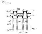
- FIG. 2 shows the control and output voltage waveforms of the VSI.
- the (time) period of the PWM carrier is denoted 105.
- the high-side and the low-side control signals 110 and 120 of a phase leg contain the low-to-high control dead-time 130 (t cd_LH ) and the high-to-low control dead-time 140 (t cd_HL ) which are inserted by the controller to avoid arm shoot-through. This effectively reduces the high switch ON time 115 and the low switch ON time 125. For safety reasons, these blanking intervals are always more than the transition time required to switch-over the phase leg.
- the output voltage 150 of the phase leg is well defined when the high- or the low side switch is controlled, but the voltage x time area (volt-seconds product) during the low-to-high 160 and the high-to-low 170 control dead-time is hard to predict.
- the output voltage depends on the output current, and may be different from the intended output voltage. If not compensated, this difference causes voltage inaccuracies and increased THD (Total Harmonic Distortion). This is most problematic if the average current is comparable to the current ripple, which happens at light load conditions. Moreover, if the current reaches zero during effective dead time, then a structure change happens and discontinuous conduction mode can occur. This means that both high- and low-side semiconductor switches in one or more of the phase legs of Figure 1 cease to conduct, and the bridge voltage U b will become equal to the grid voltage (or the back EMF (ElectroMotive Force) voltage in case of motor drives). This structure change can cause further nonlinearities.
- THD Total Harmonic Distortion
- the delays are not known exactly, and may depend on the current and the temperature of the semiconductor. Because of these, the length of the effective dead-time (t d ) can only be estimated using complex physical models or lookup tables containing past measurement data.
- Phase leg currents with switch-over events at close to zero current can be seen in the time range 174.
- an intermediate third case applies, with a required correction voltage smaller by absolute value than for the time range 176. This is so because here discontinuous conduction may happen during dead time.
- the time range 176 is usually very short, and as such, is often left uncompensated by simpler compensators.
- any dead-time compensator is to ensure that the voltage x time area at the output of each phase leg is the same as what would be if the input duty cycles were applied to an ideal, completely linear inverter.
- a good compensator decreases THD, providing sinusoidal output voltage and sinusoidal current for linear loads. This enables the control of inverters at very light loads, and enables compliance with harmonic emission standards at such load conditions. Good compensators are also required to enable the use and accurate control of sensorless drives, especially at low rotational speeds.
- the existing dead-time compensation methods can be classified as below:
- the RMS (Root Mean Squared) current and the actual-to-RMS current ratio values are applied separately to two lookup tables containing previous error measurement data values. The two results are multiplied to get the error voltage values.
- the model 210 calculates the average bridge voltages ub av which would appear at the output of the non-ideal inverter if D* is applied on it.
- the model uses voltage and current data measured at the beginning of the half period.
- the 210 model calculates with discontinuous conduction mode, dead-time, switch delays, and voltage drops too.
- the subtractor 240 calculates the difference between the output of the ideal and the non-ideal inverter, and the divider 250 divides this difference by Udc. This is then used for compensation in subtractor 260. This simple intervention can be performed fast, but it gives perfect results only in continuous conduction (high current) mode. In low current cases where the half current ripple is larger than the average current, current waveforms containing zero crossings can arise. For such cases, this formula only gives approximate results.
- a PWM VSI generally comprises in each phase a pair of semiconductor switching elements connected in series between DC voltage rails of a DC power source and a pair of diodes connected in series between the DC voltage rails of the DC power source wherein each of the diodes is connected antiparallel with a respective semiconductor switching element.
- Each phase output node is connected to an LC filter circuit.
- the method comprises the step of
- the measured parameters are the input DC voltage, the phase leg current values and the output phase voltages.
- the duty cycle of the phases not yet switched over may be corrected in the same way for a given timestamp. However, depending on the number of already switched over phases, for a given timestamp, a different correction of the duty cycle is carried out.
- the duty cycle for all of the three phases is corrected by decreasing the duty cycle of an ideal inverter (D*) by a difference value ( ⁇ D). This may be called complete correction of the duty cycle of all three phases.
- the difference value ( ⁇ D) for determining the duty cycle (D) is obtained by dividing an error voltage Uerr by the DC voltage U DC , wherein the error voltage.
- Uerr is the difference of a phase leg voltage determined on the basis of the measured parameters and of the ideal phase leg voltage Ub_ideal.
- the ideal phase leg voltage is determined by a model for an ideal inverter and the non-ideal phase leg voltage is determined by a model for a non-ideal inverter taking in to account deadtime, switch delay time, voltage drops and discontinuous conduction mode.
- the duty cycle of the two phases not yet switched over is corrected by decreasing the duty cycle of an ideal inverter (D*) by a difference value ( ⁇ D) and increasing the same by a shifting value V for changing the zero order component of the phase leg voltage vector.
- D* an ideal inverter
- ⁇ D difference value
- V shifting value
- This correction the duty cycle can be termed as partial correction.
- the number of switched-over phases is three, no correction of the duty cycle for the three phases is carried out. When all three phases are switched over, no more correction is possible. This case only occurs, if the timestamp is near to the end of a half period of the PWM carrier signal. If only one timestamp is applicable, through the proper selection of the timestamp with respect to the half period can be guaranteed that at least a partial or a full corrcetion is possible.
- a control delay time additional tn the time stamp is applied in order to determine the time of intervention, which may be used instead of the timestamp.
- the object of the invention may be achieved by using a system for compensating the dead time delay in a pulse width modulated voltage sourced inverter, PWM VSI, comprising in each phase a pair of semiconductor switching elements connected in series between DC voltage rails of a DC power source and a pair of diodes connected in series between the DC voltage rails of the DC power source wherein each of the diodes is connected antiparallel with a respective semiconductor switching element, wherein each phase output node is connected to an LC filter circuit.
- PWM VSI pulse width modulated voltage sourced inverter
- the means for carrying out an in-cycle correction of the duty cycle (D) comprises an intervention unit (460) provided a first input for receiving an ideal duty cycle value (D*) a second input for receiving timestamp values, a third input for receiving information on the number of the switched over phases, a fourth input for receiving a duty cycle difference value ( ⁇ D) and an output for the corrected duty cycle (D).
- the main advantage of the system as suggested is its ability to quickly react to changes. This is performed by providing in-cycle-intervention ability. It can be better understood with the help of Figure 6 which shows the operation of a three phase PWM modulator.
- the triangular PWM carrier 310 is compared in the modulator with the duty cycles Du1, Du2 and Du3 to generate the PWM control signal at the output of the modulator.
- the slope of the carrier is positive in the half period 330, so the phase legs switch from the high to the low side.
- the first switch-over happens at t 1 , the second at t 2 , and the third at t 3 , respectively.
- the values t 1 , t 2 , and t 3 are not static values but rather dynamic ones, oscillating between the upper and lower limits of the PWM carrier signal according to a sinusoid 3 phase AC voltage. Therefore not only the absolute position of t 1 , t 2 , and t 3 , changes, but also the relative position of these values with respect to each other. It will also be contemplated that t 1 might be equal to t 2 , while t 3 is different and t 2 might be equal to t 3 , while t 1 is different.
- the block diagram of the compensator system 400 can be seen in Figure 7 . It is very similar to the model based compensator seen in Figure 5 .
- the inputs of the system are the D* reference duty factor vector, the instantaneous currents i a , i b , i c , the DC voltage U DC , and the three grid phase voltages U P_A , U p_B and U p_C . These parameters are sampled by analog sample and hold circuits, and are then digitalized via A/D converters.
- the time stamp of the measurements is the time when the sample&hold operation was performed relative to the beginning of the actual half-period of the PWM carrier.
- the model 410 calculates the possible average bridge voltages u bA , u bB , and u bC for the actual half period of the triangular carrier if the duty cyrle vector D* is applied to a non-ideal PWM inverter having delays and voltage drops.
- the model does this estimation using all previous duty cycles from previous iterations within the actual half-period, and actual measurement data.
- the models 210, 220, 410, 420 are known from earlier publications of the inventors, therefore they will only be described in a detail necessary for the understanding of the invention.
- an intervention block 460 is applied which decides on the type of intervention used, based on the actual timestamp of the measurements and the previous duty cycle values. This is required for the in-cycle intervention ability.
- the output of the compensator is fed back to the input for the next run, as shown by the loop 490. This increases accuracy.
- the algorithm can operate continuously, in a cyclical manner. It can be run as a separate task or on a separate core of the DSP which controls the inverter.
- Relatively fast sensors are required, capable of producing inductor current measurements at a sampling frequency at least one order of magnitude higher than the switching frequency of the inverter, so that nearly instantaneous currents can be taken.
- the frequency of intervention is not locked to the switching frequency, and is only limited by the speed of the controller DSP and the current measurement unit.
- the detailed operation of the compensator system 400 can be seen in a flowchart ( Figure 8 ).
- the underlined variables in the flowchart are vectors containing three elements (one for each phase). Some steps of the flow chart have the same number as a block in Figure 7 . These correspond to the same operation.
- new instantaneous inductor current measurement values are collected, along with output phase voltage data and DC voltage in S405.
- the model 410 is run in S410 to get the average bridge voltage for the real inverter.
- the average bridge voltage for the ideal inverter is calculated in S420.
- the difference is calculated in S440, and it is scaled to duty cycle range in S450.
- step S462 checks the actual time stamp. If it is smaller than t 1 as seen in Figure 6 , no switch-over has happened so far. In this case, step S464 is executed.
- the output duty cycle D is simply a difference between the input D* and the calculated difference value ⁇ D.
- the block S466 checks if the time stamp is between t 1 and t 2 . If this is true, a switch-over has already happened in one of the phases. Based on the duty cycle values, the already switched-over phase can be identified (phase i in S468) and the corresponding difference duty cycle (labelled as V) can be used in S470, where the whole duty cycle vector is shifted with this value. This means that the duty factor of the already switched phase remains unchanged, and the correction is performed by changing the zero order component of the bridge voltage vector. This can be done in most three-phase inverters, as the neutral cable is not connected to the DC link, so the zero-order impedance is very high.
- the elements of the D output duty cycle vector are called a, b, and c, respectively.
- a, b, and c are phase quantities (in this case, duty factors)
- ⁇ and ⁇ are Descartes coordinates which define the three phase vector (here duty factor vector) in a stationary reference frame.
Landscapes
- Engineering & Computer Science (AREA)
- Power Engineering (AREA)
- Inverter Devices (AREA)
Abstract
- providing a PWM control signal for controlling the switching state of the semiconductor switching elements (SW1, SW2) in each phase leg,
- taking measurement samples of different parameters influencing the voltage (Ub) of a phase leg cyclically.
- selecting the frequency of taking the samples so that at least one sample of the parameters is taken during each half period of the PWM carrier signal,
- using the time of taking the measurement sample as a time stamp,
- determining the number of already switched over phases in each half period of the PWM carrier signal for the actual time stamp, and
- carrying out an in-cycle correction of the duty cycle (D) for the phases not yet switched over.
Description
- The invention generally relates to pulse wide modulation (PWM) controlled voltage sourced inverters (VSI) and more specifically to a method and system for dead time compensation in PWM controlled inverters and variable frequency drives.
- Nowadays, as electric cars and renewable energy sources like solar and wind generation are becoming widespread, the number of grid connected bi-directional inverters and variable frequency drives is increasing quickly. New inverters should be small and cheap, while harmonic emissions need to be kept low to conform regulations and to avoid disturbances caused by EMI if multiple inverters are used on the same grid, together with other equipment.
-
Figure 1 shows the main circuit of a conventional three phase grid connected PWM VSI (Pulse Width Modulated Voltage Source Inverter)system 1.System 1 operates between the DC-link 10 and the AC-link 20.System 1 includes three phase legs,phase leg 30 for phase "A", 33 for phase "B", and 36 for phase "C". Each phase leg, likeleg 30 consists of two semiconductor switching elements connected in series, and two semiconductor diodes connected in series, wherein each of the diodes is connected in parallel with a respective semiconductor switching element: high-side switch 50 parallel with high-side diode 60, and low-side switch 70 parallel with low-side diode 80. The semiconductor switching elements can be BJT-s (bipolar junction transistor), MOSFET-s (Metal Oxide Semiconductor Field Effect Transistor), IGBT-s (Insulated Gate Bipolar Transistor) or any other controllable semiconductor switches. The switches are controlled using a controller unit (not shown in the drawing) which normally contains a DSP (Digital Signal Processor) or an FPGA (Field Programmable Gate Array) or a purpose designed ASIC (Application Specific Integrated Circuit). Each phase leg is filtered using a filter or load containing reactive components, likeLC filter 90 for the phase "A". An inductive filter or load is always required, but capacitive filtering is also needed in grid connected applications. InFigure 1 , ubA, ubB and ubC refer to the phase leg voltages of the inverter, and iA, iB and iC refer to the output currents of the phase legs 30 (for phase A), 33 (for phase B), and 36 (for phase C), respectively. The voltages of theAC grid 20 are referenced as upA, upB and upC.Figure 1 depicts only a minimal set of components relevant to the discussion. - In ideal case sinusoidal duty cycle control of a PWM VSI would result in a sinusoidal output voltage. In practical realizations, however this is not the case. For sinusoidal duty cycle control, the output voltages are not completely sinusoidal in these inverters; these voltages always contain low order harmonics. This happens because of three main reasons:
- i.) the load dependent fluctuation of the DC bus voltage,
- ii.) the current dependent voltage drop -over the power semiconductor devices and
- iii.) the insertion of control dead time.
- The fluctuation of the DC bus voltage is usually slow and not very significant; advanced controllers can cope with this problem easily. The switching transistor and the diode voltage drops are more problematic, as these are not only current dependent, but also depend on the temperature. Even so, the problem due to these voltage drops is usually minor and can be compensated by the inverter controller using pre-recorded semiconductor forward characteristics. The most problematic cause of nonlinearities is the insertion of control dead-time by the inverter controller. This is illustrated in
Figure 2 . -
Figure 2 shows the control and output voltage waveforms of the VSI. The (time) period of the PWM carrier is denoted 105. The high-side and the low-side control signals time 115 and the low switch ONtime 125. For safety reasons, these blanking intervals are always more than the transition time required to switch-over the phase leg. Theoutput voltage 150 of the phase leg is well defined when the high- or the low side switch is controlled, but the voltage x time area (volt-seconds product) during the low-to-high 160 and the high-to-low 170 control dead-time is hard to predict. The transition time of the phase leg is equal to the difference between the off-delay (tdoff) and the on-delay (tdon) of the semiconductor switches ( tt = tdoff + tdon, not shown inFigure 2 ). What remains from the "control" dead-time inserted by the switch controller is the "effective" dead time: td = tcd -tt. During the effective dead-time, the output voltage depends on the output current, and may be different from the intended output voltage. If not compensated, this difference causes voltage inaccuracies and increased THD (Total Harmonic Distortion). This is most problematic if the average current is comparable to the current ripple, which happens at light load conditions. Moreover, if the current reaches zero during effective dead time, then a structure change happens and discontinuous conduction mode can occur. This means that both high- and low-side semiconductor switches in one or more of the phase legs ofFigure 1 cease to conduct, and the bridge voltage Ub will become equal to the grid voltage (or the back EMF (ElectroMotive Force) voltage in case of motor drives). This structure change can cause further nonlinearities. - The delays are not known exactly, and may depend on the current and the temperature of the semiconductor. Because of these, the length of the effective dead-time (td) can only be estimated using complex physical models or lookup tables containing past measurement data.
- In
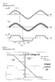
Figure 3 the distortion effects caused by dead time can be well observed. During positive phase leg current, the phase leg voltage always becomes negative during the effective dead time regardless of the direction of the switch-over, because the diode D2 will conduct. This causes a negative error voltage which needs to be compensated via adding a positive compensating voltage to the reference. For negative currents, the same effect causes a positive error voltage via opening D2. The error voltage is constant for current waveforms not containing zero crossings. Such time ranges are marked with 172. Nearly zero currents have a ripple which is positive at one switch-over, and negative at the next one. Such switch-over events produce dead time voltage errors with opposite signs, and as such, these cancel out, so no compensation is required. This is seen in thetime range 176. Phase leg currents with switch-over events at close to zero current can be seen in thetime range 174. Here an intermediate third case applies, with a required correction voltage smaller by absolute value than for thetime range 176. This is so because here discontinuous conduction may happen during dead time. Thetime range 176 is usually very short, and as such, is often left uncompensated by simpler compensators. - The main goal of any dead-time compensator is to ensure that the voltage x time area at the output of each phase leg is the same as what would be if the input duty cycles were applied to an ideal, completely linear inverter.
- A good compensator decreases THD, providing sinusoidal output voltage and sinusoidal current for linear loads. This enables the control of inverters at very light loads, and enables compliance with harmonic emission standards at such load conditions. Good compensators are also required to enable the use and accurate control of sensorless drives, especially at low rotational speeds.
- The existing dead-time compensation methods can be classified as below:
- The simplest and most accurate way of doing this is via using an accurate voltage feedback from the output of each of the phase legs (before any filtering is done). This requires fast, extra measurement hardware which is otherwise not needed for the operation of the inverter normally. As such, this solution is seldom used.
- In some cases, current direction detection is possible via measuring the sign of the voltage on the free-wheeling diodes. Patent no
US 6535402 B1 discloses such a solution. Using this method greatly decreases hardware costs, but some serious drawbacks cannot be excluded, especially at low currents (see below) or with zero crossing waveforms if the measurements are performed only at switching frequency. - Most methods so far use only the sign of the measured average current (signum(I)) and therefore cannot cope with low current problems and discontinuous conduction mode. The operation of the simplest one of such compensators can be seen in
Figure 4 .Vertical line 180 shows the characteristic of the compensator, the actual values can be calculated from the approximate effective dead-time, the switching frequency and DC link voltage. Patent no.US 6714424 B2 also discloses a method which uses signum(I). David Leggate and Russel J. Kerkman, "Pulse Based Dead Time Compensator for PWM Voltage Inverters" IEEE Transactions on Industrial Electronics (1997), vol. 44, pp. 191-197. discloses a pulse based method which is also based on this input. - There are differences in how the value of the effective dead-time is obtained. The more advanced variants of these methods use some kind of learning algorithm to approximate this value. It improves compensation. Two such methods from literature can be seen below: Seon-Hwan Hwang and Jang-Mok Kim, "Dead Time Compensation Method for Voltage-Fed PWM Inverter" IEEE Transactions on Energy Conversion (2010), vol. 25, pp. 1-10.Cichowski and J. Nieznanski "Self-tuning dead-time compensation method for voltage-source inverters" IEEE Power Electronics Letters (2005), vol. 3, pp. 72-75
- The most advanced methods try to make use of the amplitude of the current as well. Such methods found so far can be classified as analytical solutions and approximate solutions. An analytical solution is published by the inventors in A Futó, I Varjasi: "Compensation of Discontinuous Conduction in Three Phase Voltage Source PWM In verters"
In: Renewable Energy & Power Quality Journal: RE&PQJ, edited by Manuel Perez Donsion. Place and date of conference: Cordoba, Spain, 2014.04.07-2014.04.10. Cordoba: European Association for the Development of Renewable Energies, Environment and Power Quality (EA4EPQ), 2014. pp. 1-6. (International Conference on Renewable Energies and Power Quality, ICREPQ'14) (ISBN:978-84-616-8196-9). Compensating for low current cases and discontinuous conduction mode require the frequent re-calculation of complex mathematical formulae in the controller chip of the inverter. For three-phase inverters, this is very computationally intensive and impractical. - Approximate solutions use pre-recorded or approximate characteristics to improve the results. These offer somewhat better performance than signum(I), but still leave considerable inaccuracy. An example of an approximate solution is the "linear interpolation" based compensator shown by
line 190 inFigure 4 . For high currents, this method uses the signum(I) approach, but for currents lower than a pre-set limit, it compensates via using an approximate error voltage calculated from a linear interpolation between the error voltage for positive and negative currents. This improves compensation at low currents. Patent noUS 8084986 B2 discloses a similar but more advanced method. In the method the RMS (Root Mean Squared) current and the actual-to-RMS current ratio values (called "per unit" in the cited document) are applied separately to two lookup tables containing previous error measurement data values. The two results are multiplied to get the error voltage values. - To increase low current performance, a new model based compensator was published by the inventors in Andras Futo, Istvan Varjasi: "Simple Model Based Dead Time Compensation Using Fast Current Measurement" In: AASRI Conference on Circuit and Signal Processing: (CSP 2014). Place and date of conference: London, UK, 2014.06.21-2014.06.22. Elsevier, 2014. pp. 146-151. (in AASRI Procedia: http://www.sciencedirect.com/science/article/pii/S2212671614001231). The described model can be seen in
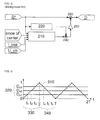
Figure 5 . The input of the compensator is the duty cycle vector D* which basically contains reference duty cycles. D* would result in the accurate output voltage vector on a theoretical ideal inverter using ideal switches with no switching delays and thus having zero transition times, controlled without control deadtime. Themodel 210 calculates the average bridge voltages ub av which would appear at the output of the non-ideal inverter if D* is applied on it. The model uses voltage and current data measured at the beginning of the half period. The 210 model calculates with discontinuous conduction mode, dead-time, switch delays, and voltage drops too. Theideal inverter block 220 calculates the bridge voltages for the ideal inverter ub ideal = (D*-½)*Udc. Thesubtractor 240 calculates the difference between the output of the ideal and the non-ideal inverter, and thedivider 250 divides this difference by Udc. This is then used for compensation insubtractor 260. This simple intervention can be performed fast, but it gives perfect results only in continuous conduction (high current) mode. In low current cases where the half current ripple is larger than the average current, current waveforms containing zero crossings can arise. For such cases, this formula only gives approximate results. - Therefore it is an object of the invention to provide an improved method and system for dead time compensation for PWM controlled inverters.
- This object may be achieved by using a method for compensating the dead time effects in a pulse wide modulated voltage sourced inverter according to
claim 1 and using a system according to claim 13. A PWM VSI, generally comprises in each phase a pair of semiconductor switching elements connected in series between DC voltage rails of a DC power source and a pair of diodes connected in series between the DC voltage rails of the DC power source wherein each of the diodes is connected antiparallel with a respective semiconductor switching element. Each phase output node is connected to an LC filter circuit. According to one aspect of the invention the method comprises the step of - providing a PWM control signal for controlling the switching state of the semiconductor switching elements in each phase leg,
- taking measurement samples of different parameters influencing the voltage (Ub) of a phase leg cyclically,
- The method is further characterized by the steps of
- selecting the frequency of taking the samples so that at least one sample of the parameters is taken during each half period of the PWM carrier signal,
- using the time of taking the measurement sample as a time stamp,
- determining the number of already switched over phases in each half period of the PWM carrier signal for the actual time stamp, and
- carrying out an in-cycle correction of the duty cycle (D) for the phases not yet switched over.
- The measured parameters are the input DC voltage, the phase leg current values and the output phase voltages.
- The duty cycle of the phases not yet switched over may be corrected in the same way for a given timestamp. However, depending on the number of already switched over phases, for a given timestamp, a different correction of the duty cycle is carried out.
- If, for a given timestamp, the number of switched-over phases is zero, the duty cycle for all of the three phases is corrected by decreasing the duty cycle of an ideal inverter (D*) by a difference value (ΔD). This may be called complete correction of the duty cycle of all three phases.
- The difference value (ΔD) for determining the duty cycle (D) is obtained by dividing an error voltage Uerr by the DC voltage UDC, wherein the error voltage. Uerr is the difference of a phase leg voltage determined on the basis of the measured parameters and of the ideal phase leg voltage Ub_ideal.
- The ideal phase leg voltage is determined by a model for an ideal inverter and the non-ideal phase leg voltage is determined by a model for a non-ideal inverter taking in to account deadtime, switch delay time, voltage drops and discontinuous conduction mode.
- If, for a given timestamp, the number of switched-over phases is one, the duty cycle of the two phases not yet switched over is corrected by decreasing the duty cycle of an ideal inverter (D*) by a difference value (ΔD) and increasing the same by a shifting value V for changing the zero order component of the phase leg voltage vector. As the duty cycle of the already switched over phase cannot be corrected this time, the remaining two phases can be corrected with respect to the already switched over phase so that whole duty cycle vector is shifted with the value V.
- If, for a given timestamp, the number of switched-over phases is two, a desired duty cycle D' of the one phase not yet switched over is calculated by decreasing the duty cycle of an ideal inverter (D*) by a difference value (ΔD) and the duty cycle nearest to the desired duty cycle is determined by minimizing an error vector E=D-D'. This correction the duty cycle can be termed as partial correction.
- And if, for a given timestamp, the number of switched-over phases is three, no correction of the duty cycle for the three phases is carried out. When all three phases are switched over, no more correction is possible. This case only occurs, if the timestamp is near to the end of a half period of the PWM carrier signal. If only one timestamp is applicable, through the proper selection of the timestamp with respect to the half period can be guaranteed that at least a partial or a full corrcetion is possible.
- Therefore it may be advantageous to increase the frequency of sample taking so that the number of timestamps during a half period of PWM carrier signal is at least three. In this case it is very likely that at least one complete correction or a partial correction of the duty cycle of the phases can be carried out.
- According to an aspect of the invention a control delay time additional tn the time stamp is applied in order to determine the time of intervention, which may be used instead of the timestamp.
- The object of the invention may be achieved by using a system for compensating the dead time delay in a pulse width modulated voltage sourced inverter, PWM VSI, comprising in each phase a pair of semiconductor switching elements connected in series between DC voltage rails of a DC power source and a pair of diodes connected in series between the DC voltage rails of the DC power source wherein each of the diodes is connected antiparallel with a respective semiconductor switching element, wherein each phase output node is connected to an LC filter circuit. The system also comprises
- a PWM modulator for providing a PWM control signal for controlling the switching state of the semiconductor switching elements (SW1, SW2) in each phase leg. The system is further chacterized by comprising
- a sample and hold unit for taking at least one measurement sample of different parameters influencing the voltage (Ub) of a phase leg cyclically during each half period of the PWM carrier signal, and for determining time stamps as the time of taking the measurement samples,
- means for determining the number of already switched over phases in each half period of the PWM carrier signal for the actual time stamp, and
- means for carrying out an in-cycle correction of the duty cycle (D) for the phases not yet switched over.
- According to an aspect of the invention, the means for carrying out an in-cycle correction of the duty cycle (D) comprises an intervention unit (460) provided a first input for receiving an ideal duty cycle value (D*) a second input for receiving timestamp values, a third input for receiving information on the number of the switched over phases, a fourth input for receiving a duty cycle difference value (ΔD) and an output for the corrected duty cycle (D).
- In order that the invention may be more readily understood, reference will now be made, by way of example, to the accompanying drawings in which:
-
Figure 1 is a circuit diagram of a general three phase two-level voltage source inverter. -
Figure 2 is a graph of the voltage waveforms of the gate drive signals of the two semiconductor switches and the bridge voltage versus time for one phase leg of a general voltage source inverter. -
Figure 3 is a diagram showing the average bridge output voltage, bridge current, and the voltage required for compensation versus time. The distortion caused by dead time is visible on the top diagram which shows the average bridge voltage for both ideal inverters with zero effective dead time (ubAV,ideal) and for real inverters with nonzero effective dead time (UbAV,real) -
Figure 4 is a graph showing the operation of two conventional dead-time compensation methods. The graph shows the estimated error voltage versus average inverter output current for a phase leg. -
Figure 5 is a schematic block diagram of a previous model based dead-time compensator system. -
Figure 6 is a graph of the triangular carrier waveform versus time used in three-phase PWM Voltage Sourced Inverters (VSI). The graph also shows the three duty cycle values, and defines time points and regions relevant for the in-cycle intervention logic. -
Figure 7 is a schematic block diagram of a model based dead time compensator system capable of in-cycle intervention. -
Figure 8 is a flow chart of a model based dead-time compensator system capable of in-cycle intervention, showing details of how the in-cycle intervention can be performed at various points of time, in a model according toFig. 7 . - The main advantage of the system as suggested is its ability to quickly react to changes. This is performed by providing in-cycle-intervention ability. It can be better understood with the help of
Figure 6 which shows the operation of a three phase PWM modulator. Thetriangular PWM carrier 310 is compared in the modulator with the duty cycles Du1, Du2 and Du3 to generate the PWM control signal at the output of the modulator. The slope of the carrier is positive in thehalf period 330, so the phase legs switch from the high to the low side. The first switch-over happens at t1, the second at t2, and the third at t3, respectively. It will be appreciated that the values t1, t2, and t3, are not static values but rather dynamic ones, oscillating between the upper and lower limits of the PWM carrier signal according to asinusoid 3 phase AC voltage. Therefore not only the absolute position of t1, t2, and t3, changes, but also the relative position of these values with respect to each other. It will also be contemplated that t1 might be equal to t2, while t3 is different and t2 might be equal to t3, while t1 is different. It might be also clear that the assignment of the times and duty cycles t1 - Du1, t2 - Du2 and t3 - Du3 is not constant, it changes with the time cyclically. The time t1 means only the first swith-over of a phase leg which might belong to a phase with the duty cycle Du1, Du2 or Du3 equally. - Full compensation is possible before t1 or (t1 = t2) because before this point of time, no switch-over has yet happened and thus all three duty factors can still be modified. Between t1 and t2, full compensation is still possible if the zero order impedance is infinite, but the zero order modulation will be changed. After t2, if t2 ≠ t3, only partial compensation is possible, and after t3 or (t2 = t3) the average output voltage for the given half-period cannot be modified anymore. The same applies for the second half-
period 340, the only difference is that the phase legs switch from the low to the high side. The compensator under discussion uses these possibilities to perform the necessary modifications to the duty cycles where possible. - The block diagram of the
compensator system 400 can be seen inFigure 7 . It is very similar to the model based compensator seen inFigure 5 . The inputs of the system are the D* reference duty factor vector, the instantaneous currents ia, ib, ic, the DC voltage UDC, and the three grid phase voltages UP_A, Up_B and Up_C. These parameters are sampled by analog sample and hold circuits, and are then digitalized via A/D converters. The time stamp of the measurements is the time when the sample&hold operation was performed relative to the beginning of the actual half-period of the PWM carrier. Themodel 410 calculates the possible average bridge voltages ubA, ubB, and ubC for the actual half period of the triangular carrier if the duty cyrle vector D* is applied to a non-ideal PWM inverter having delays and voltage drops. The model does this estimation using all previous duty cycles from previous iterations within the actual half-period, and actual measurement data. Themodels ideal inverter block 420 calculates the bridge voltages for the ideal inverter ub ideal = (D*-½)*Udc. Thesubtractor 440 calculates the difference between the output of the ideal and the non-ideal inverter Uerr = Ub ideal - Ub pred, and theblock 450 divides this difference by Udc to have duty cycle dimension D = Uerr/Udc. According to the invention anintervention block 460 is applied which decides on the type of intervention used, based on the actual timestamp of the measurements and the previous duty cycle values. This is required for the in-cycle intervention ability. The output of the compensator is fed back to the input for the next run, as shown by theloop 490. This increases accuracy. The algorithm can operate continuously, in a cyclical manner. It can be run as a separate task or on a separate core of the DSP which controls the inverter. Relatively fast sensors are required, capable of producing inductor current measurements at a sampling frequency at least one order of magnitude higher than the switching frequency of the inverter, so that nearly instantaneous currents can be taken. The frequency of intervention is not locked to the switching frequency, and is only limited by the speed of the controller DSP and the current measurement unit. - The detailed operation of the
compensator system 400 can be seen in a flowchart (Figure 8 ). The underlined variables in the flowchart are vectors containing three elements (one for each phase). Some steps of the flow chart have the same number as a block inFigure 7 . These correspond to the same operation. At the beginning of a new iteration of the compensator algorithm insystem 400, new instantaneous inductor current measurement values are collected, along with output phase voltage data and DC voltage in S405. Themodel 410 is run in S410 to get the average bridge voltage for the real inverter. The average bridge voltage for the ideal inverter is calculated in S420. The difference is calculated in S440, and it is scaled to duty cycle range in S450. - The decision block S462 checks the actual time stamp. If it is smaller than t1 as seen in
Figure 6 , no switch-over has happened so far. In this case, step S464 is executed. The output duty cycle D is simply a difference between the input D* and the calculated difference value ΔD. - Otherwise, the block S466 checks if the time stamp is between t1 and t2. If this is true, a switch-over has already happened in one of the phases. Based on the duty cycle values, the already switched-over phase can be identified (phase i in S468) and the corresponding difference duty cycle (labelled as V) can be used in S470, where the whole duty cycle vector is shifted with this value. This means that the duty factor of the already switched phase remains unchanged, and the correction is performed by changing the zero order component of the bridge voltage vector. This can be done in most three-phase inverters, as the neutral cable is not connected to the DC link, so the zero-order impedance is very high.
- If the actual time stamp is after t2, then full correction cannot be performed, but a partial correction may be possible. The block S472 decides if it is still possible to intervene in one of the duty cycles. If yes, the goal of the compensator is to calculate the duty cycle vector D closest to the desired duty cycle vector D' while only one component of D can be modified, this is D(j), labelled as W. The j index is determined in S474. D' is calculated in step S476 and an α-β transformation (also called Clarke transformation) is performed in S478 on three-phase vector D' to get α' and β'. As mentioned before, the goal is to minimize the length of an error vector E = D - D'. The elements of the D output duty cycle vector are called a, b, and c, respectively. Using the formulas of the Clarke transformation, the Clarke representation of the output can be written as:

where a, b, and c are phase quantities (in this case, duty factors) and α and β are Descartes coordinates which define the three phase vector (here duty factor vector) in a stationary reference frame. - The square of the Euclidean norm of the error vector can be written as follows:

- In the above formula, one of the three phase duty factors a, b, and c is unknown. That one is marked as W. The other two, as well as α' and β' are known variables. Thus it can be easily understood that the two polynomials in the brackets can be rewritten as the sum of a constant part (u1 and u2) plus a term proportional to W (k1*W and k2*W). Here the value W needs to be calculated. W is equal to D(j) which is one of a, b, or c depending on the j index determined in S474. The constants u1, k1, u2, and k2 can be calculated using the two already available elements of D, and using α' and β'. This is performed in S480. Using these variables, the length of the error vector can be calculated by the following equation:

- The formula for |E|2 defines an upward opening parabola. Its minimum value can be found via derivation:

- The above equation is used in S482 to calculate the final output D(j). If none of the duty cycles can be changed, the algorithm jumps from S472 to S486 and leaves the duty cycle vector unchanged. Finding the proper duty cycle values will result in proper phase voltages with a minimum of total harmonic distortion THD even under frequently changing load conditions.
- It is understood that the system and method described herein may be included in a programmable HW array such as an FPGA and transformed to hardware in the production of integrated circuits. Additionally, the apparatus and methods described herein may be embodied as a combination of hardware and software. Thus, the present invention should not be limited by any of the above-described exemplary embodiments, but should be defined only in accordance with the following claims and their equivalents.
Claims (14)
- Method for compensating the dead time in a pulse wide modulated voltage sourced inverter, PWM VSI, comprising in each phase a pair of semiconductor switching elements (SW1, SW2) connected in series between DC voltage rails of a DC power source and a pair of diodes (D1, D2) connected in series between the DC voltage rails of the DC power source wherein each of the diodes (D1, D2) is connected antiparallel with a respective semiconductor switching element (SW1, SW2), wherein each phase output node (A, B, C) is connected to an LC filter circuit, the method comprising the steps of- providing a PWM control signal for controlling the switching state of the semiconductor switching elements (SW1, SW2) in each phase leg,- taking measurement samples of different parameters influencing the voltage (Ub) of a phase leg cyclically,characterized in the further steps of- selecting the frequency of taking the samples so that at least one sample of the parameters is takenduring each half period of the PWM carrier signal,- using the time of taking the measurement sample as a time stamp,- determining the number of already switched over phases in each half period of the PWM carrier signal for the actual time stamp, and- carrying out an in-cycle correction of the duty cycle (D) for the phases not yet switched over.
- The method of claim 1, wherein the duty cycle (D) of the phases not yet switched over is corrected in the same way for a given timestamp.
- The method of claim 2, wherein a different correction of the duty cycle (D) is carried out depending on the number of already switched over phases, for a given timestamp.
- The method of claim 3, wherein, if the number of switched-over phases is zero, the duty cycle (D) for all of the three phases is corrected by decreasing the duty cycle of an ideal inverter (D*) by a difference value (ΔD).
- The method of claim 3, wherein, if the number of switched-over phases is one, the duty cycle of the two phases not yet switched over is corrected by decreasing the duty cycle of an ideal inverter (D*) by a difference value (ΔD) and increasing the same by a shifting value V for changing the zero order component of the phase leg voltage vector.
- The method of claim 3, wherein, if the number of switched-over phases is two, a desired duty cycle D' of the one phase not yet switched over is calculated by decreasing the duty cycle of an ideal inverter (D*) by a difference value (ΔD) and the duty cycle nearest to the desired duty cycle is determined by minimizing an error vector E=D-D'.
- The method of claim 3, wherein if the number of switched-over phases is three for a given timestamp, no correction of the duty cycle for the three phases is carried out.
- The method of claim 1 to 7, wherein the number of timestamps during a half period of PWM carrier signal is at least three.
- The method of claim 1 to 8, wherein a control delay time additional to the time stamp is applied order to determine the time of intervention, which may be used instead of the timestamp.
- The method of claim 4 to 6, wherein the difference value (ΔD) for determining the duty cycle (D) is obtained by dividing an error voltage Uerr by the DC voltage UDC, wherein the error voltage Uerr is the difference of a phase leg voltage determined on the basis of the measured parameters and of the ideal phase leg voltage Ub_ideal.
- The method of claim 10, wherein the measured parameters are the input DC voltage (UDC), the phase leg current values (IA, IB, IC), and the output phase voltages (UPA, UPB, UPC).
- The method of 12, wherein the ideal phase leg voltage is determined by a model for an ideal inverter and the non-ideal phase leg voltage is determined by a model for a non-ideal inverter taking in to account deadtime, switch delay time, voltage drops and discontinuous conduction mode.
- System for compensating the dead time delay in a pulse wide modulated voltage sourced inverter, PWM VSI, comprising in each phase a pair of semiconductor switching elements (SW1, SW2) connected in series between DC voltage rails of a DC power source and a pair of diodes (D1, D2) connected in series between the DC voltage rails of the DC power source wherein each of the diodes (D1, D2) is connected antiparallel with a respective semiconductor switching element (SW1, SW2), wherein each phase output node (A, B, C) is connected to an LC filter circuit the system also comprising- a PWM modulator for providing a PWM control signal for controlling the switching state of the semiconductor switching elements (SW1, SW2) in each phase leg, characterized in that the system further comprises- a sample and hold unit for taking at least one measurement sample of different parameters influencing the voltage (Ub) of a phase leg cyclically during each half period of the PWM carrier signal, and for determining time stamps as the time of taking the measurement samples,- means for determining the number of already switched over phases in each half period of the PWM carrier signal for the actual time stamp, and- means for carrying out an in-cycle correction of the duty cycle (D) for the phases not yet switched over.
- The system of claim 14, wherein the means for carrying out an in-cycle correction of the duty cycle (D) comprises an intervention unit (460) provided a first input for receiving an ideal duty cycle value (D*) a second input for receiving timestamp values, a third input for receiving information on the number of the switched over phases, a fourth input for receiving a duty cycle difference value (ΔD) and an output for the corrected duty cycle (D).
Priority Applications (2)
| Application Number | Priority Date | Filing Date | Title |
|---|---|---|---|
| EP15462002.5A EP3104516B1 (en) | 2015-06-09 | 2015-06-09 | Method and system for dead time compensation in a pwm controlled inverter |
| HUE15462002A HUE037964T2 (en) | 2015-06-09 | 2015-06-09 | Method and system for dead time compensation in a pwm controlled inverter |
Applications Claiming Priority (1)
| Application Number | Priority Date | Filing Date | Title |
|---|---|---|---|
| EP15462002.5A EP3104516B1 (en) | 2015-06-09 | 2015-06-09 | Method and system for dead time compensation in a pwm controlled inverter |
Publications (2)
| Publication Number | Publication Date |
|---|---|
| EP3104516A1 true EP3104516A1 (en) | 2016-12-14 |
| EP3104516B1 EP3104516B1 (en) | 2018-03-21 |
Family
ID=53510823
Family Applications (1)
| Application Number | Title | Priority Date | Filing Date |
|---|---|---|---|
| EP15462002.5A Not-in-force EP3104516B1 (en) | 2015-06-09 | 2015-06-09 | Method and system for dead time compensation in a pwm controlled inverter |
Country Status (2)
| Country | Link |
|---|---|
| EP (1) | EP3104516B1 (en) |
| HU (1) | HUE037964T2 (en) |
Cited By (12)
| Publication number | Priority date | Publication date | Assignee | Title |
|---|---|---|---|---|
| CN108390553A (en) * | 2018-02-08 | 2018-08-10 | 江西精骏电控技术有限公司 | A kind of compensation method in the dead zones motor drive PWM |
| CN111988021A (en) * | 2019-05-24 | 2020-11-24 | 北京车和家信息技术有限公司 | PWM generation method and device, motor controller and vehicle |
| WO2021066996A1 (en) * | 2019-10-04 | 2021-04-08 | Borgwarner Inc. | Method of duty cycle generation for extending the linear modulation range in a pulse width modulated voltage source inverter |
| CN113702742A (en) * | 2021-08-30 | 2021-11-26 | 广东技术师范大学 | System and method for testing electromagnetic immunity under dynamic working conditions of vehicle |
| CN114070096A (en) * | 2021-11-11 | 2022-02-18 | 中冶赛迪电气技术有限公司 | Current interruption compensation method for AC-AC frequency converter |
| US11394334B2 (en) * | 2019-02-18 | 2022-07-19 | Nissan Motor Co., Ltd. | Power control method and power control apparatus |
| CN115833541A (en) * | 2022-12-09 | 2023-03-21 | 上海儒竞智控技术有限公司 | PWM wave generation and duty ratio control method, system, timer and storage medium |
| CN115913023A (en) * | 2022-11-03 | 2023-04-04 | 苏州伟创电气科技股份有限公司 | Voltage compensation method and voltage compensation device |
| CN116896285A (en) * | 2023-09-11 | 2023-10-17 | 湖南大学 | A hybrid carrier modulation method for multi-level converters |
| CN117713501A (en) * | 2023-12-19 | 2024-03-15 | 河北建投新能源有限公司 | Modulation method, modulation device, terminal and storage medium of bidirectional current source type converter |
| CN118432099A (en) * | 2024-04-28 | 2024-08-02 | 南方电网科学研究院有限责任公司 | A distributed harmonic control closed-loop control method, device and system |
| CN120825044A (en) * | 2025-09-12 | 2025-10-21 | 南京欧陆电气股份有限公司 | A precise dead-zone compensation method for SVPWM based on oscilloscope phase markers |
Families Citing this family (1)
| Publication number | Priority date | Publication date | Assignee | Title |
|---|---|---|---|---|
| US11923795B2 (en) | 2022-02-15 | 2024-03-05 | Haier Us Appliance Solutions, Inc. | System and method for voltage calibration |
Citations (5)
| Publication number | Priority date | Publication date | Assignee | Title |
|---|---|---|---|---|
| US6535402B1 (en) | 2002-07-12 | 2003-03-18 | Delta Electronics Inc. | Adaptive compensation of dead time for inverter and converter |
| US6714424B2 (en) | 2001-11-30 | 2004-03-30 | Ballard Power Systems Corporation | Dead-time compensation with narrow pulse elimination in solid- state switch devices |
| US8084986B2 (en) | 2009-12-28 | 2011-12-27 | Delta Electronics, Inc. | Dead-time compensation apparatus of PWM inverter and method thereof |
| DE102012112902A1 (en) * | 2011-12-23 | 2013-06-27 | Sma Solar Technology Ag | Method for controlling multi-phase inverter bridge switches of inverter for photovoltaic system, involves setting upper fixed value by adding another correction value, if predetermined upper threshold value exceeds duty cycle |
| US20150077025A1 (en) * | 2013-09-18 | 2015-03-19 | Denso Corporation | Power conversion apparatus and electric power steering apparatus having the same |
-
2015
- 2015-06-09 EP EP15462002.5A patent/EP3104516B1/en not_active Not-in-force
- 2015-06-09 HU HUE15462002A patent/HUE037964T2/en unknown
Patent Citations (5)
| Publication number | Priority date | Publication date | Assignee | Title |
|---|---|---|---|---|
| US6714424B2 (en) | 2001-11-30 | 2004-03-30 | Ballard Power Systems Corporation | Dead-time compensation with narrow pulse elimination in solid- state switch devices |
| US6535402B1 (en) | 2002-07-12 | 2003-03-18 | Delta Electronics Inc. | Adaptive compensation of dead time for inverter and converter |
| US8084986B2 (en) | 2009-12-28 | 2011-12-27 | Delta Electronics, Inc. | Dead-time compensation apparatus of PWM inverter and method thereof |
| DE102012112902A1 (en) * | 2011-12-23 | 2013-06-27 | Sma Solar Technology Ag | Method for controlling multi-phase inverter bridge switches of inverter for photovoltaic system, involves setting upper fixed value by adding another correction value, if predetermined upper threshold value exceeds duty cycle |
| US20150077025A1 (en) * | 2013-09-18 | 2015-03-19 | Denso Corporation | Power conversion apparatus and electric power steering apparatus having the same |
Non-Patent Citations (9)
| Title |
|---|
| "Renewable Energy & Power Quality Journal: RE&PQJ", MANUEL PEREZ DONSION |
| A FUTO; I VARJASI, COMPENSATION OF DISCONTINUOUS CONDUCTION IN THREE PHASE VOLTAGE SOURCE PWM INVERTERS |
| ANDRAS FUTO; ISTVAN VARJASI: "A AASRI Conference on Circuit and Signal Processing: (CSP 2014", 21 June 2014, ELSEVIER, article "Simple Model Based Dead Time Compensation Using Fast Current Meaasurement", pages: 146 - 151 |
| CICHOWSKI; J. NLIEZNANSKI: "Znif-ttin;nn dead-time compensationme for voltage-source inverters", IEEE POWER ELECTRONICS LETTERS, vol. 3, 2005, pages 72 - 75 |
| DAVID LEGGATE; RUSSEL J. KERKMAN: "Pulse Based Dead Time Compensator for PWM Voltage Inverters", IEEE TRANSACTIONS ON INDUSTRIAL ELECTRONICS, vol. 44, 1997, pages 191 - 197, XP000586504 * |
| DAVID LEGGATE; RUSSEL J. KERKMAN: "Pulse Based Dead Time Compensator for PWM Voltage Inverters", IEEE TRANSACTIONS ON INDUSTRIAL ELECTRONICS, vol. 44, 1997, pages 191 - 197, XP011023245 |
| INTERNATIONAL CONFERENCE ON RENEWABLE ENERGIES AND POWER QUALITY, ICREPQ'14, 2014, pages 1 - 6 |
| SEON-HWAN HWANG; JANG-MOK KIM: "Dead Time Compensation Method for Voltage-Fed PWM Inverter", IEEE TRANSACTIONS ON ENERGY CONVERSION, vol. 25, 2010, pages 1 - 10, XP011284269, DOI: doi:10.1109/TEC.2009.2031811 |
| SEON-HWAN HWANG; JANG-MOK KIM: "Dead Time Compensation Method for Voltage-Fed PWM Inverter", IEEE TRANSACTIONS ON ENERGY CONVERSION, vol. 25, March 2010 (2010-03-01), pages 1 - 10, XP011297054 * |
Cited By (17)
| Publication number | Priority date | Publication date | Assignee | Title |
|---|---|---|---|---|
| CN108390553A (en) * | 2018-02-08 | 2018-08-10 | 江西精骏电控技术有限公司 | A kind of compensation method in the dead zones motor drive PWM |
| US11394334B2 (en) * | 2019-02-18 | 2022-07-19 | Nissan Motor Co., Ltd. | Power control method and power control apparatus |
| CN111988021B (en) * | 2019-05-24 | 2024-05-03 | 北京车和家信息技术有限公司 | PWM generation method and device, motor controller and vehicle |
| CN111988021A (en) * | 2019-05-24 | 2020-11-24 | 北京车和家信息技术有限公司 | PWM generation method and device, motor controller and vehicle |
| WO2021066996A1 (en) * | 2019-10-04 | 2021-04-08 | Borgwarner Inc. | Method of duty cycle generation for extending the linear modulation range in a pulse width modulated voltage source inverter |
| US11239787B2 (en) | 2019-10-04 | 2022-02-01 | Borgwarner Inc. | Method of duty cycle generation for extending the linear modulation range in a pulse width modulated voltage source inverter |
| CN114097171A (en) * | 2019-10-04 | 2022-02-25 | 博格华纳公司 | Duty cycle generation method for extending linear modulation range in pulse width modulation voltage source inverter |
| CN113702742A (en) * | 2021-08-30 | 2021-11-26 | 广东技术师范大学 | System and method for testing electromagnetic immunity under dynamic working conditions of vehicle |
| CN114070096A (en) * | 2021-11-11 | 2022-02-18 | 中冶赛迪电气技术有限公司 | Current interruption compensation method for AC-AC frequency converter |
| CN114070096B (en) * | 2021-11-11 | 2024-05-14 | 中冶赛迪电气技术有限公司 | A method for current discontinuity compensation of AC-AC inverter |
| CN115913023A (en) * | 2022-11-03 | 2023-04-04 | 苏州伟创电气科技股份有限公司 | Voltage compensation method and voltage compensation device |
| CN115833541A (en) * | 2022-12-09 | 2023-03-21 | 上海儒竞智控技术有限公司 | PWM wave generation and duty ratio control method, system, timer and storage medium |
| CN116896285B (en) * | 2023-09-11 | 2023-11-14 | 湖南大学 | Mixed carrier modulation method of multi-level converter |
| CN116896285A (en) * | 2023-09-11 | 2023-10-17 | 湖南大学 | A hybrid carrier modulation method for multi-level converters |
| CN117713501A (en) * | 2023-12-19 | 2024-03-15 | 河北建投新能源有限公司 | Modulation method, modulation device, terminal and storage medium of bidirectional current source type converter |
| CN118432099A (en) * | 2024-04-28 | 2024-08-02 | 南方电网科学研究院有限责任公司 | A distributed harmonic control closed-loop control method, device and system |
| CN120825044A (en) * | 2025-09-12 | 2025-10-21 | 南京欧陆电气股份有限公司 | A precise dead-zone compensation method for SVPWM based on oscilloscope phase markers |
Also Published As
| Publication number | Publication date |
|---|---|
| HUE037964T2 (en) | 2018-09-28 |
| EP3104516B1 (en) | 2018-03-21 |
Similar Documents
| Publication | Publication Date | Title |
|---|---|---|
| EP3104516B1 (en) | Method and system for dead time compensation in a pwm controlled inverter | |
| KR101512188B1 (en) | A driving method of the modular multi-level converter and the apparatus thereof | |
| Yusoff et al. | A concept of virtual-flux direct power control of three-phase AC-DC converter | |
| Chang et al. | An analytical approach for characterizing harmonic and interharmonic currents generated by VSI-fed adjustable speed drives | |
| Wang et al. | Online feedback dead time compensation strategy for three-level T-type inverters | |
| Trinh et al. | An improved control strategy of three-phase PWM rectifiers under input voltage distortions and DC-offset measurement errors | |
| Hoffmann et al. | Observer-based grid voltage disturbance rejection for grid connected voltage source PWM converters with line side LCL filters | |
| CN104980040A (en) | Power converterpower converting apparatus control device of power converterpower converting apparatus and control method of power converterpower converting apparatus | |
| KR101929519B1 (en) | Three level neutral point clamped inverter system having imbalance capacitor voltages and its control method | |
| Briz et al. | Current sampling and measurement in PWM operated AC drives and power converters | |
| US10666131B2 (en) | Dead-time voltage compensation apparatus and dead-time voltage compensation method | |
| US10826411B2 (en) | Device for controlling power conversion circuit | |
| Zeng et al. | Development of an SVPWM-based predictive current controller for three-phase grid-connected VSI | |
| Zeng et al. | Improved current controller based on SVPWM for three-phase grid-connected voltage source inverters | |
| US11611286B2 (en) | Method for determining rectifier-stage output current or grid-side currents of a frequency converter | |
| KR102399873B1 (en) | Apparatus and method for measuring current of 3-phase pulse width modulation(PWM) inverter | |
| Rojas et al. | Instantaneous average prediction of the currents in a PWM-controlled two-level converter | |
| JP2011172387A (en) | Power conversion controller, converter control circuit, power conversion control method, power conversion control program and recording medium | |
| Majić et al. | Influence of dead time on voltage harmonic spectrum of grid-connected PWM-VSC with LCL filter | |
| Mallik et al. | DC link voltage sensorless control of a three-phase boost power factor correction rectifier | |
| Lin et al. | Model-free predictive current control of a voltage source inverter | |
| Gakis et al. | Simple control schemes for grid-connected three-phase voltage-source inverters of DG units | |
| Kim et al. | Indirect-modulated MMC current control with voltage disturbance estimation and compensation | |
| Zare et al. | A new hysteresis current control for three-phase inverters based on adjacent voltage vectors and time error | |
| Jin et al. | Current ripple reduction for finite control set model predictive control strategy of grid-tied inverter with reference current compensation |
Legal Events
| Date | Code | Title | Description |
|---|---|---|---|
| PUAI | Public reference made under article 153(3) epc to a published international application that has entered the european phase |
Free format text: ORIGINAL CODE: 0009012 |
|
| AK | Designated contracting states |
Kind code of ref document: A1 Designated state(s): AL AT BE BG CH CY CZ DE DK EE ES FI FR GB GR HR HU IE IS IT LI LT LU LV MC MK MT NL NO PL PT RO RS SE SI SK SM TR |
|
| AX | Request for extension of the european patent |
Extension state: BA ME |
|
| 17P | Request for examination filed |
Effective date: 20170125 |
|
| RBV | Designated contracting states (corrected) |
Designated state(s): AL AT BE BG CH CY CZ DE DK EE ES FI FR GB GR HR HU IE IS IT LI LT LU LV MC MK MT NL NO PL PT RO RS SE SI SK SM TR |
|
| GRAP | Despatch of communication of intention to grant a patent |
Free format text: ORIGINAL CODE: EPIDOSNIGR1 |
|
| INTG | Intention to grant announced |
Effective date: 20171017 |
|
| GRAS | Grant fee paid |
Free format text: ORIGINAL CODE: EPIDOSNIGR3 |
|
| GRAA | (expected) grant |
Free format text: ORIGINAL CODE: 0009210 |
|
| AK | Designated contracting states |
Kind code of ref document: B1 Designated state(s): AL AT BE BG CH CY CZ DE DK EE ES FI FR GB GR HR HU IE IS IT LI LT LU LV MC MK MT NL NO PL PT RO RS SE SI SK SM TR |
|
| REG | Reference to a national code |
Ref country code: GB Ref legal event code: FG4D |
|
| REG | Reference to a national code |
Ref country code: CH Ref legal event code: EP |
|
| REG | Reference to a national code |
Ref country code: AT Ref legal event code: REF Ref document number: 982119 Country of ref document: AT Kind code of ref document: T Effective date: 20180415 |
|
| REG | Reference to a national code |
Ref country code: IE Ref legal event code: FG4D |
|
| REG | Reference to a national code |
Ref country code: DE Ref legal event code: R096 Ref document number: 602015009070 Country of ref document: DE |
|
| REG | Reference to a national code |
Ref country code: NL Ref legal event code: MP Effective date: 20180321 |
|
| PG25 | Lapsed in a contracting state [announced via postgrant information from national office to epo] |
Ref country code: NO Free format text: LAPSE BECAUSE OF FAILURE TO SUBMIT A TRANSLATION OF THE DESCRIPTION OR TO PAY THE FEE WITHIN THE PRESCRIBED TIME-LIMIT Effective date: 20180621 Ref country code: HR Free format text: LAPSE BECAUSE OF FAILURE TO SUBMIT A TRANSLATION OF THE DESCRIPTION OR TO PAY THE FEE WITHIN THE PRESCRIBED TIME-LIMIT Effective date: 20180321 Ref country code: LT Free format text: LAPSE BECAUSE OF FAILURE TO SUBMIT A TRANSLATION OF THE DESCRIPTION OR TO PAY THE FEE WITHIN THE PRESCRIBED TIME-LIMIT Effective date: 20180321 Ref country code: CY Free format text: LAPSE BECAUSE OF FAILURE TO SUBMIT A TRANSLATION OF THE DESCRIPTION OR TO PAY THE FEE WITHIN THE PRESCRIBED TIME-LIMIT Effective date: 20180321 Ref country code: FI Free format text: LAPSE BECAUSE OF FAILURE TO SUBMIT A TRANSLATION OF THE DESCRIPTION OR TO PAY THE FEE WITHIN THE PRESCRIBED TIME-LIMIT Effective date: 20180321 |
|
| REG | Reference to a national code |
Ref country code: LT Ref legal event code: MG4D |
|
| REG | Reference to a national code |
Ref country code: AT Ref legal event code: MK05 Ref document number: 982119 Country of ref document: AT Kind code of ref document: T Effective date: 20180321 |
|
| PG25 | Lapsed in a contracting state [announced via postgrant information from national office to epo] |
Ref country code: GR Free format text: LAPSE BECAUSE OF FAILURE TO SUBMIT A TRANSLATION OF THE DESCRIPTION OR TO PAY THE FEE WITHIN THE PRESCRIBED TIME-LIMIT Effective date: 20180622 Ref country code: SE Free format text: LAPSE BECAUSE OF FAILURE TO SUBMIT A TRANSLATION OF THE DESCRIPTION OR TO PAY THE FEE WITHIN THE PRESCRIBED TIME-LIMIT Effective date: 20180321 Ref country code: RS Free format text: LAPSE BECAUSE OF FAILURE TO SUBMIT A TRANSLATION OF THE DESCRIPTION OR TO PAY THE FEE WITHIN THE PRESCRIBED TIME-LIMIT Effective date: 20180321 Ref country code: LV Free format text: LAPSE BECAUSE OF FAILURE TO SUBMIT A TRANSLATION OF THE DESCRIPTION OR TO PAY THE FEE WITHIN THE PRESCRIBED TIME-LIMIT Effective date: 20180321 Ref country code: BG Free format text: LAPSE BECAUSE OF FAILURE TO SUBMIT A TRANSLATION OF THE DESCRIPTION OR TO PAY THE FEE WITHIN THE PRESCRIBED TIME-LIMIT Effective date: 20180621 |
|
| REG | Reference to a national code |
Ref country code: HU Ref legal event code: AG4A Ref document number: E037964 Country of ref document: HU |
|
| PG25 | Lapsed in a contracting state [announced via postgrant information from national office to epo] |
Ref country code: EE Free format text: LAPSE BECAUSE OF FAILURE TO SUBMIT A TRANSLATION OF THE DESCRIPTION OR TO PAY THE FEE WITHIN THE PRESCRIBED TIME-LIMIT Effective date: 20180321 Ref country code: PL Free format text: LAPSE BECAUSE OF FAILURE TO SUBMIT A TRANSLATION OF THE DESCRIPTION OR TO PAY THE FEE WITHIN THE PRESCRIBED TIME-LIMIT Effective date: 20180321 Ref country code: IT Free format text: LAPSE BECAUSE OF FAILURE TO SUBMIT A TRANSLATION OF THE DESCRIPTION OR TO PAY THE FEE WITHIN THE PRESCRIBED TIME-LIMIT Effective date: 20180321 Ref country code: AL Free format text: LAPSE BECAUSE OF FAILURE TO SUBMIT A TRANSLATION OF THE DESCRIPTION OR TO PAY THE FEE WITHIN THE PRESCRIBED TIME-LIMIT Effective date: 20180321 Ref country code: ES Free format text: LAPSE BECAUSE OF FAILURE TO SUBMIT A TRANSLATION OF THE DESCRIPTION OR TO PAY THE FEE WITHIN THE PRESCRIBED TIME-LIMIT Effective date: 20180321 Ref country code: RO Free format text: LAPSE BECAUSE OF FAILURE TO SUBMIT A TRANSLATION OF THE DESCRIPTION OR TO PAY THE FEE WITHIN THE PRESCRIBED TIME-LIMIT Effective date: 20180321 Ref country code: NL Free format text: LAPSE BECAUSE OF FAILURE TO SUBMIT A TRANSLATION OF THE DESCRIPTION OR TO PAY THE FEE WITHIN THE PRESCRIBED TIME-LIMIT Effective date: 20180321 |
|
| PG25 | Lapsed in a contracting state [announced via postgrant information from national office to epo] |
Ref country code: AT Free format text: LAPSE BECAUSE OF FAILURE TO SUBMIT A TRANSLATION OF THE DESCRIPTION OR TO PAY THE FEE WITHIN THE PRESCRIBED TIME-LIMIT Effective date: 20180321 Ref country code: CZ Free format text: LAPSE BECAUSE OF FAILURE TO SUBMIT A TRANSLATION OF THE DESCRIPTION OR TO PAY THE FEE WITHIN THE PRESCRIBED TIME-LIMIT Effective date: 20180321 Ref country code: SK Free format text: LAPSE BECAUSE OF FAILURE TO SUBMIT A TRANSLATION OF THE DESCRIPTION OR TO PAY THE FEE WITHIN THE PRESCRIBED TIME-LIMIT Effective date: 20180321 Ref country code: SM Free format text: LAPSE BECAUSE OF FAILURE TO SUBMIT A TRANSLATION OF THE DESCRIPTION OR TO PAY THE FEE WITHIN THE PRESCRIBED TIME-LIMIT Effective date: 20180321 |
|
| PG25 | Lapsed in a contracting state [announced via postgrant information from national office to epo] |
Ref country code: PT Free format text: LAPSE BECAUSE OF FAILURE TO SUBMIT A TRANSLATION OF THE DESCRIPTION OR TO PAY THE FEE WITHIN THE PRESCRIBED TIME-LIMIT Effective date: 20180723 |
|
| REG | Reference to a national code |
Ref country code: DE Ref legal event code: R119 Ref document number: 602015009070 Country of ref document: DE |
|
| REG | Reference to a national code |
Ref country code: DE Ref legal event code: R097 Ref document number: 602015009070 Country of ref document: DE |
|
| PLBE | No opposition filed within time limit |
Free format text: ORIGINAL CODE: 0009261 |
|
| STAA | Information on the status of an ep patent application or granted ep patent |
Free format text: STATUS: NO OPPOSITION FILED WITHIN TIME LIMIT |
|
| PG25 | Lapsed in a contracting state [announced via postgrant information from national office to epo] |
Ref country code: DK Free format text: LAPSE BECAUSE OF FAILURE TO SUBMIT A TRANSLATION OF THE DESCRIPTION OR TO PAY THE FEE WITHIN THE PRESCRIBED TIME-LIMIT Effective date: 20180321 |
|
| REG | Reference to a national code |
Ref country code: CH Ref legal event code: PL |
|
| 26N | No opposition filed |
Effective date: 20190102 |
|
| REG | Reference to a national code |
Ref country code: BE Ref legal event code: MM Effective date: 20180630 |
|
| REG | Reference to a national code |
Ref country code: IE Ref legal event code: MM4A |
|
| PG25 | Lapsed in a contracting state [announced via postgrant information from national office to epo] |
Ref country code: LU Free format text: LAPSE BECAUSE OF NON-PAYMENT OF DUE FEES Effective date: 20180609 Ref country code: MC Free format text: LAPSE BECAUSE OF FAILURE TO SUBMIT A TRANSLATION OF THE DESCRIPTION OR TO PAY THE FEE WITHIN THE PRESCRIBED TIME-LIMIT Effective date: 20180321 |
|
| PG25 | Lapsed in a contracting state [announced via postgrant information from national office to epo] |
Ref country code: DE Free format text: LAPSE BECAUSE OF NON-PAYMENT OF DUE FEES Effective date: 20190101 Ref country code: CH Free format text: LAPSE BECAUSE OF NON-PAYMENT OF DUE FEES Effective date: 20180630 Ref country code: IE Free format text: LAPSE BECAUSE OF NON-PAYMENT OF DUE FEES Effective date: 20180609 Ref country code: LI Free format text: LAPSE BECAUSE OF NON-PAYMENT OF DUE FEES Effective date: 20180630 Ref country code: FR Free format text: LAPSE BECAUSE OF NON-PAYMENT OF DUE FEES Effective date: 20180630 |
|
| PG25 | Lapsed in a contracting state [announced via postgrant information from national office to epo] |
Ref country code: SI Free format text: LAPSE BECAUSE OF FAILURE TO SUBMIT A TRANSLATION OF THE DESCRIPTION OR TO PAY THE FEE WITHIN THE PRESCRIBED TIME-LIMIT Effective date: 20180321 Ref country code: BE Free format text: LAPSE BECAUSE OF NON-PAYMENT OF DUE FEES Effective date: 20180630 |
|
| PGFP | Annual fee paid to national office [announced via postgrant information from national office to epo] |
Ref country code: HU Payment date: 20190604 Year of fee payment: 5 |
|
| PG25 | Lapsed in a contracting state [announced via postgrant information from national office to epo] |
Ref country code: MT Free format text: LAPSE BECAUSE OF NON-PAYMENT OF DUE FEES Effective date: 20180609 |
|
| GBPC | Gb: european patent ceased through non-payment of renewal fee |
Effective date: 20190609 |
|
| PG25 | Lapsed in a contracting state [announced via postgrant information from national office to epo] |
Ref country code: TR Free format text: LAPSE BECAUSE OF FAILURE TO SUBMIT A TRANSLATION OF THE DESCRIPTION OR TO PAY THE FEE WITHIN THE PRESCRIBED TIME-LIMIT Effective date: 20180321 |
|
| PG25 | Lapsed in a contracting state [announced via postgrant information from national office to epo] |
Ref country code: GB Free format text: LAPSE BECAUSE OF NON-PAYMENT OF DUE FEES Effective date: 20190609 |
|
| PG25 | Lapsed in a contracting state [announced via postgrant information from national office to epo] |
Ref country code: MK Free format text: LAPSE BECAUSE OF NON-PAYMENT OF DUE FEES Effective date: 20180321 |
|
| PG25 | Lapsed in a contracting state [announced via postgrant information from national office to epo] |
Ref country code: IS Free format text: LAPSE BECAUSE OF FAILURE TO SUBMIT A TRANSLATION OF THE DESCRIPTION OR TO PAY THE FEE WITHIN THE PRESCRIBED TIME-LIMIT Effective date: 20180721 |
|
| PG25 | Lapsed in a contracting state [announced via postgrant information from national office to epo] |
Ref country code: HU Free format text: LAPSE BECAUSE OF NON-PAYMENT OF DUE FEES Effective date: 20200610 |