EP3104449B1 - Two-dimensional electronically steerable antenna - Google Patents
Two-dimensional electronically steerable antenna Download PDFInfo
- Publication number
- EP3104449B1 EP3104449B1 EP16171450.6A EP16171450A EP3104449B1 EP 3104449 B1 EP3104449 B1 EP 3104449B1 EP 16171450 A EP16171450 A EP 16171450A EP 3104449 B1 EP3104449 B1 EP 3104449B1
- Authority
- EP
- European Patent Office
- Prior art keywords
- ferrite
- magnetizing
- controller
- path
- elements
- Prior art date
- Legal status (The legal status is an assumption and is not a legal conclusion. Google has not performed a legal analysis and makes no representation as to the accuracy of the status listed.)
- Active
Links
Images


Classifications
-
- H—ELECTRICITY
- H01—ELECTRIC ELEMENTS
- H01Q—ANTENNAS, i.e. RADIO AERIALS
- H01Q3/00—Arrangements for changing or varying the orientation or the shape of the directional pattern of the waves radiated from an antenna or antenna system
- H01Q3/26—Arrangements for changing or varying the orientation or the shape of the directional pattern of the waves radiated from an antenna or antenna system varying the relative phase or relative amplitude of energisation between two or more active radiating elements; varying the distribution of energy across a radiating aperture
- H01Q3/30—Arrangements for changing or varying the orientation or the shape of the directional pattern of the waves radiated from an antenna or antenna system varying the relative phase or relative amplitude of energisation between two or more active radiating elements; varying the distribution of energy across a radiating aperture varying the relative phase between the radiating elements of an array
- H01Q3/34—Arrangements for changing or varying the orientation or the shape of the directional pattern of the waves radiated from an antenna or antenna system varying the relative phase or relative amplitude of energisation between two or more active radiating elements; varying the distribution of energy across a radiating aperture varying the relative phase between the radiating elements of an array by electrical means
- H01Q3/36—Arrangements for changing or varying the orientation or the shape of the directional pattern of the waves radiated from an antenna or antenna system varying the relative phase or relative amplitude of energisation between two or more active radiating elements; varying the distribution of energy across a radiating aperture varying the relative phase between the radiating elements of an array by electrical means with variable phase-shifters
-
- H—ELECTRICITY
- H01—ELECTRIC ELEMENTS
- H01P—WAVEGUIDES; RESONATORS, LINES, OR OTHER DEVICES OF THE WAVEGUIDE TYPE
- H01P1/00—Auxiliary devices
- H01P1/165—Auxiliary devices for rotating the plane of polarisation
-
- H—ELECTRICITY
- H01—ELECTRIC ELEMENTS
- H01P—WAVEGUIDES; RESONATORS, LINES, OR OTHER DEVICES OF THE WAVEGUIDE TYPE
- H01P1/00—Auxiliary devices
- H01P1/18—Phase-shifters
- H01P1/182—Waveguide phase-shifters
-
- H—ELECTRICITY
- H01—ELECTRIC ELEMENTS
- H01P—WAVEGUIDES; RESONATORS, LINES, OR OTHER DEVICES OF THE WAVEGUIDE TYPE
- H01P1/00—Auxiliary devices
- H01P1/18—Phase-shifters
- H01P1/19—Phase-shifters using a ferromagnetic device
-
- H—ELECTRICITY
- H01—ELECTRIC ELEMENTS
- H01P—WAVEGUIDES; RESONATORS, LINES, OR OTHER DEVICES OF THE WAVEGUIDE TYPE
- H01P1/00—Auxiliary devices
- H01P1/18—Phase-shifters
- H01P1/19—Phase-shifters using a ferromagnetic device
- H01P1/195—Phase-shifters using a ferromagnetic device having a toroidal shape
-
- H—ELECTRICITY
- H01—ELECTRIC ELEMENTS
- H01Q—ANTENNAS, i.e. RADIO AERIALS
- H01Q3/00—Arrangements for changing or varying the orientation or the shape of the directional pattern of the waves radiated from an antenna or antenna system
- H01Q3/26—Arrangements for changing or varying the orientation or the shape of the directional pattern of the waves radiated from an antenna or antenna system varying the relative phase or relative amplitude of energisation between two or more active radiating elements; varying the distribution of energy across a radiating aperture
- H01Q3/30—Arrangements for changing or varying the orientation or the shape of the directional pattern of the waves radiated from an antenna or antenna system varying the relative phase or relative amplitude of energisation between two or more active radiating elements; varying the distribution of energy across a radiating aperture varying the relative phase between the radiating elements of an array
- H01Q3/34—Arrangements for changing or varying the orientation or the shape of the directional pattern of the waves radiated from an antenna or antenna system varying the relative phase or relative amplitude of energisation between two or more active radiating elements; varying the distribution of energy across a radiating aperture varying the relative phase between the radiating elements of an array by electrical means
-
- H—ELECTRICITY
- H01—ELECTRIC ELEMENTS
- H01Q—ANTENNAS, i.e. RADIO AERIALS
- H01Q3/00—Arrangements for changing or varying the orientation or the shape of the directional pattern of the waves radiated from an antenna or antenna system
- H01Q3/44—Arrangements for changing or varying the orientation or the shape of the directional pattern of the waves radiated from an antenna or antenna system varying the electric or magnetic characteristics of reflecting, refracting, or diffracting devices associated with the radiating element
-
- H—ELECTRICITY
- H01—ELECTRIC ELEMENTS
- H01P—WAVEGUIDES; RESONATORS, LINES, OR OTHER DEVICES OF THE WAVEGUIDE TYPE
- H01P5/00—Coupling devices of the waveguide type
- H01P5/12—Coupling devices having more than two ports
-
- H—ELECTRICITY
- H01—ELECTRIC ELEMENTS
- H01Q—ANTENNAS, i.e. RADIO AERIALS
- H01Q15/00—Devices for reflection, refraction, diffraction or polarisation of waves radiated from an antenna, e.g. quasi-optical devices
- H01Q15/24—Polarising devices; Polarisation filters
- H01Q15/242—Polarisation converters
- H01Q15/246—Polarisation converters rotating the plane of polarisation of a linear polarised wave
Definitions
- antenna beam-steering has been accomplished using mechanical positioners, multiple beam antennas, and active phased-arrays.
- Mechanical positioners have been used to direct a single antenna in the desired direction.
- the mechanical positioner is essentially a robot that moves the antenna in the azimuth (left, right) and elevation (up, down) directions to achieve the desired antenna position.
- Mechanical positioners are not preferred due to maintenance requirements, speed limitations, and the reliability of the rotary joints.
- Multiple-beam antennas use multiple separate antennas pointed in different directions and switch between the separate antennas. Since the use of a large number of individual antennas is not practical, lower gain antennas are traditionally used to cover a wider area. The gain for multiple-beam antennas is further reduced at beam cross-over points. For some applications, the reduction of gain for multiple-beam antennas excludes them as a viable option.
- Phased-arrays include a large number of antenna elements (e.g., transmit/receive (T/R) modules) arranged in a plane.
- T/R transmit/receive
- phased-arrays are expensive because hundreds or thousands of antenna elements are required and the spacing becomes a difficult and expensive constraint to meet because the wavelengths are small.
- United States Patent 5,729,239 discloses a voltage controlled ferroelectric lens phase array, where voltage is applied across each pair of plates to control the phase of an electromagnetic signal.
- United States Patent 3,080,536 discloses a microwave phase shifter having a magnetic circuit of saturable ferrite material in a waveguide.
- United states Patent 3,205,501 discloses a reciprocal ferromagnetic phase shifting transmission system, where a controllable magnetic field is applied to a ferrite slab for controlling the degree of phase shift.
- Embodiments of the present disclosure provide systems for a two-dimensional electronically steerable antenna and will be understood by reading a studying the following specification.
- a ferrite controller comprises: a single array of two or more ferrite control elements, wherein the ferrite control elements each include: a radio frequency (RF) path assembly including a RF path ferrite element and a RF path dielectric element.
- RF radio frequency
- the ferrite control elements also include a magnetizing ferrite assembly including: a magnetizing ferrite element configured to control the magnetization state of the control element; one or more structural dielectric elements; and a flexible insulated waveguide wall; wherein the magnetizing ferrite element is attached to the one or more structural dielectric elements, wherein the flexible insulated waveguide wall surrounds the magnetizing ferrite element and the structural dielectric elements, wherein the RF path ferrite element and the magnetizing ferrite element are attached to form a ferrite toroid.
- the ferrite control elements also include two tapered impedance matching transformers attached to the RF path assembly and the magnetizing ferrite assembly.
- Embodiments of the present disclosure provide systems and methods that overcome the above described challenges with traditional antenna beam-steering by separating the elevation and azimuth steering into different stages and utilizing at least one ferrite controller that includes an array of ferrite elements.
- Each ferrite element may replace a whole row or column of antenna elements in a traditional phased-array.
- the number of elements used to provide the desired gain and coverage for millimeter-wave frequencies is manageable.
- an antenna based on embodiments of the present disclosure only requires N row + N column antenna elements, as opposed to N row x N column antenna elements for a phased-array, because embodiments can be implemented having only a single column and a single row of antenna elements.
- the impact of a one-half wavelength or less spacing requirement is reduced compared to the phased-arrays because each separate stage only needs to accommodate this requirement in a single direction.
- the antenna elements in the single row of elements need only be spaced one-half wavelength horizontally because there are no elements vertically adjacent to the single row of elements.
- the antenna elements in the single column of elements need only be spaced one-half wavelength vertically because there are no elements horizontally adjacent to the single column of elements.
- Embodiments discussed herein thus provide systems for antenna beam-steering having reduced cost and complexity compared to traditional phased-arrays and better performance than mechanical positioners and multiple-beam antennas.
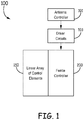
- FIGs 1 and 2 illustrate an example two-dimensional electronically steerable antenna 100 according to one embodiment of the present disclosure.
- Antenna 100 comprises an antenna controller 101, a ferrite controller 200 including a plurality of ferrite elements, one or more driver circuits 103 for each ferrite element, and a linear array of control elements 150.
- driver circuits 103 may also be electrically coupled to each control element 150 in order to independently control the phase of RF propagating through each control element 150.
- Figure 2 does not show the driver circuits 103.
- the control elements 150 include a column of phase shifting elements 106 attached to a column of parallel plates 108.
- the control elements 150 are attached to a waveguide input 102 and an E-plane power divider 104.
- the elevation steering and the azimuth steering of a beam are performed in separate stages. That is, the elevation and azimuth steering are performed by separate distinct groups of control elements, rather than a single plane of control elements. Specifically, the elevation and azimuth steering are performed by a single row of control elements and a single column of control elements.
- the linear array of control elements 150 is configured to provide elevation steering and the ferrite controller 200 is configured to provide azimuth steering.
- the two-dimensional electronically steerable antenna 100 can be rotated 90 degrees such that the linear array of control elements 150 is configured to provide azimuth steering and the ferrite controller 200 is configured to provide elevation steering.
- FIG 3 is a perspective view of an example ferrite controller 200 according to one embodiment of the present disclosure.
- the ferrite controller 200 comprises a plurality of ferrite control elements 201, also referred to herein as ferrite phase shifters. Figures 3A-3D will be referenced when describing the features of the ferrite control elements 201 in greater detail.
- the ferrite controller 200 can include a single array of two or more ferrite control elements 201 depending on the desired gain for the particular application.
- the number of ferrite control elements 201 determines the size of the ferrite controller 200 and the amount of gain that can be achieved. Thus, the greater the number of ferrite elements 201, the more precise the beam and the greater the gain.
- the ferrite control elements 201 have a height of at least five inches so they can be used to replace an entire column or row of antenna elements. For exemplary high-frequency applications (e.g., above 30 GHz), typically a height of five to fifteen inches would be used to produce the desired gain and precision.
- the E-field of the incident RF is oriented as shown in Figure 3 .
- FIG 3A is an exploded horizontal cross-section view of a ferrite control element 201 of an example ferrite controller 200 taken along the line A-A.
- Each ferrite control element 201 includes a radio frequency (RF) path assembly 202, a magnetizing ferrite assembly 205, and impedance matching transformers 212.
- RF radio frequency
- the RF path assembly 202 includes a RF path ferrite element 203 and a RF path dielectric element 204.
- the RF path ferrite element 203 and the RF path dielectric element 204 are formed as slabs having a substantially rectangular cross-section.
- the RF path ferrite element 203 also has a central portion that extends beyond the RF path dielectric element 204.
- the RF path ferrite element 203 and the RF path dielectric element 204 are each precisely manufactured to have a desired thickness because the thickness of the RF path ferrite element 203 and the RF path dielectric element 204 corresponds to a desired phase shift at the desired RF frequency.
- the RF path dielectric element 204 comprises a microwave dielectric or another dielectric material used for antenna applications known to those having skill in the art.
- the RF path ferrite element 203 and the RF path dielectric element 204 are attached together.
- the RF path ferrite element 203 and the RF path dielectric element 204 are bonded using a heat press technique or other methods known to one having skill in the art.
- the RF path assembly 202 is machined to interface with the impedance matching transformers 212.
- the magnetizing ferrite assembly 205 includes a magnetizing ferrite element 206, structural dielectric elements 208, and a flexible insulated waveguide wall 210.
- the magnetizing ferrite element 206 is formed as a slab having a thickness that is at least as thick as the RF path ferrite element 203. This thickness specification prevents flux limitations in the RF path during operation of the ferrite controller 200.
- the magnetizing ferrite element 206 is isolated from the RF path by the flexible insulated waveguide wall 210.
- the magnetizing ferrite element 206 is used to control the magnetization state of the ferrite control element 201 and thus the phase of the RF propagating through the RF path assembly 202.
- Figure 3B is a vertical cross-section view of two adjacent ferrite control elements 201 of an example ferrite controller 200 taken along the line B-B.
- the magnetizing ferrite element 206 is etched and plated with a conductive material to form a conductor 214 that continuously wraps around the magnetizing ferrite element 206 in a spiral pattern.
- the number of turns of the conductor 214 and width of the conductor 214 is selected to be an amount that will evenly distribute an applied current along the height of the magnetizing ferrite element 206.
- Figure 3B shows a particular configuration of the conductor 214 according to one embodiment of the present disclosure. The spaces in between the conductor 214 windings are exposed sections of the magnetizing ferrite element 206. It should be understood that the conductor 214 may have any configuration that would evenly distribute an applied current along the height of the magnetizing ferrite element 206.
- the structural dielectric elements 208 are attached to the magnetizing ferrite element 206 as shown in Figure 3A .
- the structural dielectric elements 208 are chosen to be thermally matched to the magnetizing ferrite element 206.
- the structural dielectric elements 208 are substantially wedge-shaped to aid in impedance transformation.
- the magnetizing ferrite element 206 and the structural dielectric elements 208 may be bonded together using a heat press technique or other methods known to those having skill in the art.
- the flexible insulated waveguide wall 210 is wrapped around the magnetizing ferrite element 206 and the structural dielectric elements 208.
- the flexible insulated waveguide wall 210 directs the incident RF energy through the RF path assembly 202.
- the flexible insulated waveguide wall 210 comprises a multi-layer film.
- flexible insulated waveguide wall 210 comprises a conductive layer 302 attached to an insulating layer 304.
- the conductive layer 302 comprises a copper sheet or another suitable conductive metal.
- the insulating layer 304 comprises a polyimide film such as Kapton or another suitable insulting material known to those having skill in the art.
- the insulating layer 304 is also adhesive. In other embodiments, an additional adhesive layer comprising a suitable adhesive material is attached to the insulating layer 304.
- the insulating layer 304 separates the conductive layer 302, which serves as the waveguide wall, from the conductor 214 wrapped around the magnetizing ferrite element 206.
- the flexible insulated waveguide wall 210 is selected so there are no horizontal breaks as it is wrapped around the magnetizing ferrite element 206 and the structural dielectric elements 208 because this can cause degraded performance. For example, if the flexible insulated waveguide wall 210 were on a roll, then a horizontal break would not occur if the roll was as wide as the ferrite controller 200 is tall.
- the magnetizing ferrite assembly 205 is attached to the RF path assembly 202.
- the magnetizing ferrite assembly 205 and the RF path assembly 202 are bonded together using a heat press technique or other methods known to those having skill in the art.
- the RF path ferrite element 203 can be bonded to the flexible insulated waveguide wall 210 and the magnetizing ferrite element 206.
- end segments 217 of the magnetizing ferrite element 206 and the RF path ferrite element 203 extend beyond the flexible insulated waveguide wall 210. It should be understood that these end segments are omitted from Figure 2 for ease of illustration. These end segments 217 of the magnetizing ferrite element 206 and the RF path ferrite element 203 extend outwardly from each end of the flexible insulated waveguide wall 210. These end segments of the magnetizing ferrite element 206 and the RF path ferrite element 203 are connected with ferrite 216 and attached to form a ferrite toroid.
- the dashed lines in Figure 3B represent where the ferrite 216 is placed between the magnetizing ferrite element 206 and the RF path ferrite element 203.
- the end segments 217 also provide access to the conductor 214 for the driver circuit 103 for that ferrite control element 201.
- the surfaces 218, 220 of the end segments 217 unique to the magnetizing ferrite element 206 that extend outwardly from each end of the flexible insulated waveguide wall 210 are used as contact points for the driver circuit 103 for that ferrite control element 201.
- the surfaces 218, 220 are etched and plated with the conductor 214, and the at least one driver circuit 103 is electrically coupled to the conductor 214.
- the height of the end segments 217 of the magnetizing ferrite element 206 and the RF path ferrite element 203 that extend beyond the flexible insulated waveguide wall 210 can also be staggered for the respective ferrite control elements 201.
- half of each end segment 217 of the magnetizing ferrite element 206 and the RF path ferrite element 203 of a respective ferrite control element 201 extend farther beyond the flexible insulated waveguide wall 210 than the other half of each end segment 217 of the magnetizing ferrite element 206 and the RF path ferrite element 203.
- This pattern can be alternated between adjacent ferrite control elements 201 to so the staggering allows easier access to the conductors 214.
- the impedance matching transformers 212 are tapered to accommodate a broad range of frequencies and wide elevation angles of RF propagation from the elevation control elements 150. Further, the impedance matching transformers 212 have a low dielectric constant so they are not as sensitive to glue line variations. In prior systems including twin-slab ferrite phase shifters, quarter-wave transformers are used. However, quarter-wave transformers do not perform as well as the tapered impedance matching transformers at wide angles. In exemplary embodiments, the impedance matching transformers 212 are composed of multiple separate pieces for ease of manufacturability. In other embodiments, the impedance matching transformers 212 are a single piece. The impedance matching transformers 212 are attached to the RF path assembly 202 and magnetizing ferrite assembly 205 after those components of the ferrite controller 200 have been attached together.
- Figure 3D is an example assembled ferrite controller 200 with three ferrite control elements 201.
- ferrite controller 200 can include two or more ferrite control elements depending on the desired precision and gain of the particular application.
- the ferrite control elements 201 contain the same components as the ferrite control elements 201 described above.
- the magnetizing ferrite assembly of an adjacent ferrite controller is attached to the RF path assembly and the impedance matching transformers.
- the magnetizing ferrite assembly of ferrite control element 201-2 is attached to the RF path assembly and impedance matching transformers of ferrite control element 201-1.
- an additional magnetizing ferrite assembly 306 is attached to the last ferrite control element 201-3 for structural purposes. Specifically, the additional magnetizing ferrite assembly 306 provides a waveguide wall for the RF that propagates through the RF path assembly of ferrite control element 201-3.
- the components of adjacent ferrite control elements are spaced a distance apart that is less than or equal to one-half wavelength of the shortest wavelength of a wave to pass through the ferrite controller 200.
- the tips of the impedance matching transformers of ferrite control element 201-1 are spaced a distance apart from the tips of the impedance matching transformers of ferrite control element 201-2 that is less than or equal to one-half wavelength of the shortest wavelength of a wave to pass through the ferrite controller 200.
- the spacing would be 0.5 centimeters or less.
- the other features of adjacent ferrite control elements are also spaced the same distance apart. This spacing prevents undesirable grating lobes. For some applications, a greater than one-half wavelength spacing can be used if grating lobes are small enough or tolerable.
- the driver circuit 103 for each ferrite control element 201 is electrically coupled to the conductor 214 that is wrapped around the magnetizing ferrite element 206 to control the phase of each ferrite control element 201.
- the antenna controller 101 calculates the delta phase between the ferrite toroids that will produce the desired azimuth steering.
- the antenna controller 101 provides a digital command to the driver circuits 103, which is converted into a voltage pulse by the driver circuits 103.
- the driver circuits 103 applies an initial saturating voltage pulse to each magnetizing ferrite element 206 in a single direction before applying a controlled non-saturating pulse in the opposite direction to set the magnetization or phase state of the ferrite toroid.
- the saturating voltage pulse can be applied in either a clockwise or counter-clockwise direction.
- the non-saturating pulse finely controls the magnetization state of each ferrite control element 201 and implements the delta phases that were calculated.
- the ferrite toroids can be magnetized using voltages of less than 200 V.
- FIG. 4 is a block diagram of an example two-dimensional electronically steerable antenna 400 according to one embodiment of the present disclosure.
- Antenna 400 includes a ferrite elevation controller 402, a 90 degree twist polarizer 404, a ferrite azimuth controller 406, and at least one driver circuit 408 per control element in each ferrite controller 402, 406.
- Ferrite elevation controller 402 and ferrite azimuth controller 406 include the same features as those discussed above with respect to ferrite controller 200. Thus, only the differences in operation will be discussed.
- the ferrite elevation controller 402 is rotated 90 degrees with respect to the ferrite azimuth controller 406.
- the ferrite elevation controller 402 is configured to control the elevation angle of a RF wave and the ferrite azimuth controller 406 is configured to control the azimuth angle of the RF wave.
- the polarizer 404 is coupled between the ferrite elevation controller 402 and the ferrite azimuth controller 406 in order to align the E-field of the RF wave prior to propagation through the ferrite azimuth controller 406.
- azimuth steering can be performed in the first stage and elevation steering can be performed in the second stage.
- the operation of the driver circuits 408 is similar to the operation of the driver circuits 103, discussed above with reference to Figures 1-3D .
- the antenna controller 401 calculates phases for each ferrite control element 201 in both ferrite controllers 402, 406, and sends digital commands to the driver circuits 408.
- the driver circuits 408 initially magnetize each ferrite control element 201 in both the ferrite elevation controller 402 and the ferrite azimuth controller 406 with saturating voltage pulses followed by precisely-controlled non-saturating pulses in the opposite direction.
- the controllers 101, 401, and the driver circuits 103, 408, include or function with software programs, firmware or other computer readable instructions for carrying out various methods, process tasks, calculations, and control functions, used in controlling the above described two-dimensional antennas 100, 400.
- system elements, method steps, or examples described throughout this disclosure may be implemented on one or more computer systems, field programmable gate array (FPGA), or similar devices comprising a processor and memory hardware executing code to realize those elements, processes, or examples, said code stored on a non-transient data storage device. Therefore other embodiments of the present disclosure may include such a processor and memory hardware as well as elements comprising program instructions resident on computer readable media which when implemented by such computer systems, enable them to implement the embodiments described herein.
- FPGA field programmable gate array
- computer readable media refers to tangible memory storage devices having non-transient physical forms.
- Such non-transient physical forms may include computer memory devices, such as but not limited to punch cards, magnetic disk or tape, any optical data storage system, flash read only memory (ROM), non-volatile ROM, programmable ROM (PROM), erasable-programmable ROM (E-PROM), random access memory (RAM), or any other form of permanent, semi-permanent, or temporary memory storage system or device having a physical, tangible form.
- Program instructions include, but are not limited to computer-executable instructions executed by computer system processors and hardware description languages such as Very High Speed Integrated Circuit (VHSIC) Hardware Description Language (VHDL).
- VHSIC Very High Speed Integrated Circuit
- VHDL Hardware Description Language
Landscapes
- Variable-Direction Aerials And Aerial Arrays (AREA)
Description
- Traditionally, antenna beam-steering has been accomplished using mechanical positioners, multiple beam antennas, and active phased-arrays. Mechanical positioners have been used to direct a single antenna in the desired direction. The mechanical positioner is essentially a robot that moves the antenna in the azimuth (left, right) and elevation (up, down) directions to achieve the desired antenna position. Mechanical positioners are not preferred due to maintenance requirements, speed limitations, and the reliability of the rotary joints.
- Multiple-beam antennas use multiple separate antennas pointed in different directions and switch between the separate antennas. Since the use of a large number of individual antennas is not practical, lower gain antennas are traditionally used to cover a wider area. The gain for multiple-beam antennas is further reduced at beam cross-over points. For some applications, the reduction of gain for multiple-beam antennas excludes them as a viable option.
- Phased-arrays include a large number of antenna elements (e.g., transmit/receive (T/R) modules) arranged in a plane. For millimeter-wave frequencies (above 30 GHz), phased-arrays are expensive because hundreds or thousands of antenna elements are required and the spacing becomes a difficult and expensive constraint to meet because the wavelengths are small.
- For the reasons stated above and for other reasons stated below which will become apparent to those skilled in the art upon reading and understanding the specification, there is a need in the art for improved systems and methods for two-dimensional antenna beam-steering at millimeter-wave frequencies.
- United States Patent
5,729,239 discloses a voltage controlled ferroelectric lens phase array, where voltage is applied across each pair of plates to control the phase of an electromagnetic signal. United States Patent3,080,536 discloses a microwave phase shifter having a magnetic circuit of saturable ferrite material in a waveguide. United states Patent3,205,501 discloses a reciprocal ferromagnetic phase shifting transmission system, where a controllable magnetic field is applied to a ferrite slab for controlling the degree of phase shift. - The Embodiments of the present disclosure provide systems for a two-dimensional electronically steerable antenna and will be understood by reading a studying the following specification.
- In one embodiment, a ferrite controller comprises: a single array of two or more ferrite control elements, wherein the ferrite control elements each include: a radio frequency (RF) path assembly including a RF path ferrite element and a RF path dielectric element. The ferrite control elements also include a magnetizing ferrite assembly including: a magnetizing ferrite element configured to control the magnetization state of the control element; one or more structural dielectric elements; and a flexible insulated waveguide wall; wherein the magnetizing ferrite element is attached to the one or more structural dielectric elements, wherein the flexible insulated waveguide wall surrounds the magnetizing ferrite element and the structural dielectric elements, wherein the RF path ferrite element and the magnetizing ferrite element are attached to form a ferrite toroid. The ferrite control elements also include two tapered impedance matching transformers attached to the RF path assembly and the magnetizing ferrite assembly.
- Understanding that the drawings depict only exemplary embodiments and are not therefore to be considered limiting in scope, the exemplary embodiments will be described with additional specificity and detail through the use of the accompanying drawings, in which:
-
Figure 1 is a block diagram of an example two-dimensional electronically steerable antenna according to one embodiment of the present disclosure. -
Figure 2 is a perspective view of an example two-dimensional electronically steerable antenna according to one embodiment of the present disclosure. -
Figure 3 is a perspective view of an example ferrite controller according to one embodiment of the present disclosure. -
Figure 3A is an exploded horizontal cross-section of a ferrite control element of an example ferrite controller according to one embodiment of the present disclosure. -
Figure 3B is a vertical cross-section of two ferrite control elements of an example ferrite controller according to one embodiment of the present disclosure. -
Figure 3C is a cross-section of an insulated waveguide wall according to one embodiment of the present disclosure. -
Figure 3D is a horizontal cross-section of an example ferrite controller according to one embodiment of the present disclosure. -
Figure 4 is a block diagram of an example two-dimensional electronically steerable antenna according to one embodiment of the present disclosure. - In accordance with common practice, the various described features are not drawn to scale but are drawn to emphasize specific features relevant to the exemplary embodiments.
- In the following detailed description, reference is made to the accompanying drawings that form a part hereof, and in which is shown by way of illustration specific illustrative embodiments. However, it is to be understood that other embodiments may be utilized and that logical, mechanical, and electrical changes may be made. Furthermore, the method presented in the drawing figures and the specification is not to be construed as limiting the order in which the individual steps may be performed. The following detailed description is, therefore, not to be taken in a limiting sense.
- Embodiments of the present disclosure provide systems and methods that overcome the above described challenges with traditional antenna beam-steering by separating the elevation and azimuth steering into different stages and utilizing at least one ferrite controller that includes an array of ferrite elements. Each ferrite element may replace a whole row or column of antenna elements in a traditional phased-array. Thus, the number of elements used to provide the desired gain and coverage for millimeter-wave frequencies is manageable. For example, an antenna based on embodiments of the present disclosure only requires Nrow + Ncolumn antenna elements, as opposed to Nrow x Ncolumn antenna elements for a phased-array, because embodiments can be implemented having only a single column and a single row of antenna elements.
- Further, the impact of a one-half wavelength or less spacing requirement is reduced compared to the phased-arrays because each separate stage only needs to accommodate this requirement in a single direction. For example, the antenna elements in the single row of elements need only be spaced one-half wavelength horizontally because there are no elements vertically adjacent to the single row of elements. Likewise, the antenna elements in the single column of elements need only be spaced one-half wavelength vertically because there are no elements horizontally adjacent to the single column of elements.
- Embodiments discussed herein thus provide systems for antenna beam-steering having reduced cost and complexity compared to traditional phased-arrays and better performance than mechanical positioners and multiple-beam antennas.
-
Figures 1 and2 illustrate an example two-dimensional electronicallysteerable antenna 100 according to one embodiment of the present disclosure.Antenna 100 comprises anantenna controller 101, aferrite controller 200 including a plurality of ferrite elements, one ormore driver circuits 103 for each ferrite element, and a linear array ofcontrol elements 150. In some embodiments,driver circuits 103 may also be electrically coupled to eachcontrol element 150 in order to independently control the phase of RF propagating through eachcontrol element 150. For ease of illustration,Figure 2 does not show thedriver circuits 103. - In exemplary embodiments, the
control elements 150 include a column ofphase shifting elements 106 attached to a column ofparallel plates 108. Thecontrol elements 150 are attached to awaveguide input 102 and anE-plane power divider 104. In the embodiment shown inFigure 2 , the elevation steering and the azimuth steering of a beam are performed in separate stages. That is, the elevation and azimuth steering are performed by separate distinct groups of control elements, rather than a single plane of control elements. Specifically, the elevation and azimuth steering are performed by a single row of control elements and a single column of control elements. In the embodiment shown inFigure 2 , the linear array ofcontrol elements 150 is configured to provide elevation steering and theferrite controller 200 is configured to provide azimuth steering. In another implementation, the two-dimensional electronicallysteerable antenna 100 can be rotated 90 degrees such that the linear array ofcontrol elements 150 is configured to provide azimuth steering and theferrite controller 200 is configured to provide elevation steering. -
Figure 3 is a perspective view of anexample ferrite controller 200 according to one embodiment of the present disclosure. Theferrite controller 200 comprises a plurality offerrite control elements 201, also referred to herein as ferrite phase shifters.Figures 3A-3D will be referenced when describing the features of theferrite control elements 201 in greater detail. It should be understood that theferrite controller 200 can include a single array of two or moreferrite control elements 201 depending on the desired gain for the particular application. The number offerrite control elements 201 determines the size of theferrite controller 200 and the amount of gain that can be achieved. Thus, the greater the number offerrite elements 201, the more precise the beam and the greater the gain. In exemplary embodiments, theferrite control elements 201 have a height of at least five inches so they can be used to replace an entire column or row of antenna elements. For exemplary high-frequency applications (e.g., above 30 GHz), typically a height of five to fifteen inches would be used to produce the desired gain and precision. For proper operation offerrite controller 200, the E-field of the incident RF is oriented as shown inFigure 3 . -
Figure 3A is an exploded horizontal cross-section view of aferrite control element 201 of anexample ferrite controller 200 taken along the line A-A. Eachferrite control element 201 includes a radio frequency (RF)path assembly 202, a magnetizingferrite assembly 205, andimpedance matching transformers 212. - The
RF path assembly 202 includes a RFpath ferrite element 203 and a RF pathdielectric element 204. The RFpath ferrite element 203 and the RF pathdielectric element 204 are formed as slabs having a substantially rectangular cross-section. In exemplary embodiments, the RFpath ferrite element 203 also has a central portion that extends beyond the RF pathdielectric element 204. The RFpath ferrite element 203 and the RF pathdielectric element 204 are each precisely manufactured to have a desired thickness because the thickness of the RFpath ferrite element 203 and the RF pathdielectric element 204 corresponds to a desired phase shift at the desired RF frequency. In exemplary embodiments, the RF pathdielectric element 204 comprises a microwave dielectric or another dielectric material used for antenna applications known to those having skill in the art. The RFpath ferrite element 203 and the RF pathdielectric element 204 are attached together. In exemplary embodiments, the RFpath ferrite element 203 and the RF pathdielectric element 204 are bonded using a heat press technique or other methods known to one having skill in the art. After attaching the RFpath ferrite element 203 and the RF pathdielectric element 204, theRF path assembly 202 is machined to interface with theimpedance matching transformers 212. - The magnetizing
ferrite assembly 205 includes a magnetizingferrite element 206, structuraldielectric elements 208, and a flexibleinsulated waveguide wall 210. The magnetizingferrite element 206 is formed as a slab having a thickness that is at least as thick as the RFpath ferrite element 203. This thickness specification prevents flux limitations in the RF path during operation of theferrite controller 200. The magnetizingferrite element 206 is isolated from the RF path by the flexibleinsulated waveguide wall 210. The magnetizingferrite element 206 is used to control the magnetization state of theferrite control element 201 and thus the phase of the RF propagating through theRF path assembly 202. -
Figure 3B is a vertical cross-section view of two adjacentferrite control elements 201 of anexample ferrite controller 200 taken along the line B-B. In exemplary embodiments, the magnetizingferrite element 206 is etched and plated with a conductive material to form aconductor 214 that continuously wraps around the magnetizingferrite element 206 in a spiral pattern. The number of turns of theconductor 214 and width of theconductor 214 is selected to be an amount that will evenly distribute an applied current along the height of the magnetizingferrite element 206.Figure 3B shows a particular configuration of theconductor 214 according to one embodiment of the present disclosure. The spaces in between theconductor 214 windings are exposed sections of the magnetizingferrite element 206. It should be understood that theconductor 214 may have any configuration that would evenly distribute an applied current along the height of the magnetizingferrite element 206. - The structural
dielectric elements 208 are attached to the magnetizingferrite element 206 as shown inFigure 3A . The structuraldielectric elements 208 are chosen to be thermally matched to the magnetizingferrite element 206. In exemplary embodiments, the structuraldielectric elements 208 are substantially wedge-shaped to aid in impedance transformation. In exemplary embodiments, the magnetizingferrite element 206 and the structuraldielectric elements 208 may be bonded together using a heat press technique or other methods known to those having skill in the art. - The flexible
insulated waveguide wall 210 is wrapped around the magnetizingferrite element 206 and the structuraldielectric elements 208. The flexibleinsulated waveguide wall 210 directs the incident RF energy through theRF path assembly 202. The flexibleinsulated waveguide wall 210 comprises a multi-layer film. For example, in an embodiment shown inFigure 3C , flexibleinsulated waveguide wall 210 comprises aconductive layer 302 attached to an insulatinglayer 304. Theconductive layer 302 comprises a copper sheet or another suitable conductive metal. For low-loss implementations, a highly conductive metal, such as gold, silver, or aluminum, would be preferable. The insulatinglayer 304 comprises a polyimide film such as Kapton or another suitable insulting material known to those having skill in the art. In some embodiments, the insulatinglayer 304 is also adhesive. In other embodiments, an additional adhesive layer comprising a suitable adhesive material is attached to the insulatinglayer 304. The insulatinglayer 304 separates theconductive layer 302, which serves as the waveguide wall, from theconductor 214 wrapped around the magnetizingferrite element 206. The flexibleinsulated waveguide wall 210 is selected so there are no horizontal breaks as it is wrapped around the magnetizingferrite element 206 and the structuraldielectric elements 208 because this can cause degraded performance. For example, if the flexibleinsulated waveguide wall 210 were on a roll, then a horizontal break would not occur if the roll was as wide as theferrite controller 200 is tall. - The magnetizing
ferrite assembly 205 is attached to theRF path assembly 202. In exemplary embodiments, the magnetizingferrite assembly 205 and theRF path assembly 202 are bonded together using a heat press technique or other methods known to those having skill in the art. Specifically, the RFpath ferrite element 203 can be bonded to the flexibleinsulated waveguide wall 210 and the magnetizingferrite element 206. - As shown in
Figure 3 andFigure 3B , endsegments 217 of the magnetizingferrite element 206 and the RFpath ferrite element 203 extend beyond the flexibleinsulated waveguide wall 210. It should be understood that these end segments are omitted fromFigure 2 for ease of illustration. Theseend segments 217 of the magnetizingferrite element 206 and the RFpath ferrite element 203 extend outwardly from each end of the flexibleinsulated waveguide wall 210. These end segments of the magnetizingferrite element 206 and the RFpath ferrite element 203 are connected withferrite 216 and attached to form a ferrite toroid. The dashed lines inFigure 3B represent where theferrite 216 is placed between the magnetizingferrite element 206 and the RFpath ferrite element 203. - The
end segments 217 also provide access to theconductor 214 for thedriver circuit 103 for thatferrite control element 201. Thesurfaces end segments 217 unique to the magnetizingferrite element 206 that extend outwardly from each end of the flexibleinsulated waveguide wall 210 are used as contact points for thedriver circuit 103 for thatferrite control element 201. In such embodiments, thesurfaces conductor 214, and the at least onedriver circuit 103 is electrically coupled to theconductor 214. The height of theend segments 217 of the magnetizingferrite element 206 and the RFpath ferrite element 203 that extend beyond the flexibleinsulated waveguide wall 210 can also be staggered for the respectiveferrite control elements 201. For example, as shown inFigures 3 and3B , half of eachend segment 217 of the magnetizingferrite element 206 and the RFpath ferrite element 203 of a respectiveferrite control element 201 extend farther beyond the flexibleinsulated waveguide wall 210 than the other half of eachend segment 217 of the magnetizingferrite element 206 and the RFpath ferrite element 203. This pattern can be alternated between adjacentferrite control elements 201 to so the staggering allows easier access to theconductors 214. - In exemplary embodiments, the
impedance matching transformers 212 are tapered to accommodate a broad range of frequencies and wide elevation angles of RF propagation from theelevation control elements 150. Further, theimpedance matching transformers 212 have a low dielectric constant so they are not as sensitive to glue line variations. In prior systems including twin-slab ferrite phase shifters, quarter-wave transformers are used. However, quarter-wave transformers do not perform as well as the tapered impedance matching transformers at wide angles. In exemplary embodiments, theimpedance matching transformers 212 are composed of multiple separate pieces for ease of manufacturability. In other embodiments, theimpedance matching transformers 212 are a single piece. Theimpedance matching transformers 212 are attached to theRF path assembly 202 and magnetizingferrite assembly 205 after those components of theferrite controller 200 have been attached together. -
Figure 3D is an example assembledferrite controller 200 with threeferrite control elements 201. As discussed above, it should be understood thatferrite controller 200 can include two or more ferrite control elements depending on the desired precision and gain of the particular application. Theferrite control elements 201 contain the same components as theferrite control elements 201 described above. To connect the assembledferrite control elements 201 to one another, the magnetizing ferrite assembly of an adjacent ferrite controller is attached to the RF path assembly and the impedance matching transformers. For example, inFigure 3D , the magnetizing ferrite assembly of ferrite control element 201-2 is attached to the RF path assembly and impedance matching transformers of ferrite control element 201-1. To complete theferrite controller 200, an additional magnetizingferrite assembly 306 is attached to the last ferrite control element 201-3 for structural purposes. Specifically, the additional magnetizingferrite assembly 306 provides a waveguide wall for the RF that propagates through the RF path assembly of ferrite control element 201-3. - The components of adjacent ferrite control elements are spaced a distance apart that is less than or equal to one-half wavelength of the shortest wavelength of a wave to pass through the
ferrite controller 200. For example, the tips of the impedance matching transformers of ferrite control element 201-1 are spaced a distance apart from the tips of the impedance matching transformers of ferrite control element 201-2 that is less than or equal to one-half wavelength of the shortest wavelength of a wave to pass through theferrite controller 200. For example, for a one centimeter wavelength (30 GHz), the spacing would be 0.5 centimeters or less. The other features of adjacent ferrite control elements are also spaced the same distance apart. This spacing prevents undesirable grating lobes. For some applications, a greater than one-half wavelength spacing can be used if grating lobes are small enough or tolerable. - As discussed above, the
driver circuit 103 for eachferrite control element 201 is electrically coupled to theconductor 214 that is wrapped around the magnetizingferrite element 206 to control the phase of eachferrite control element 201. Theantenna controller 101 calculates the delta phase between the ferrite toroids that will produce the desired azimuth steering. Theantenna controller 101 provides a digital command to thedriver circuits 103, which is converted into a voltage pulse by thedriver circuits 103. Thedriver circuits 103 applies an initial saturating voltage pulse to each magnetizingferrite element 206 in a single direction before applying a controlled non-saturating pulse in the opposite direction to set the magnetization or phase state of the ferrite toroid. In exemplary embodiments, the saturating voltage pulse can be applied in either a clockwise or counter-clockwise direction. The non-saturating pulse finely controls the magnetization state of eachferrite control element 201 and implements the delta phases that were calculated. - This technique utilizes the unique property of ferrite toroids that they will hold a magnetization indefinitely, so constantly supplied voltage is not necessary to magnetize the ferrite phase shifters, only a voltage pulse. This significantly reduces the power necessary to control the phase of the
ferrite controller 200. In exemplary embodiments, the ferrite toroids can be magnetized using voltages of less than 200 V. -
Figure 4 is a block diagram of an example two-dimensional electronicallysteerable antenna 400 according to one embodiment of the present disclosure.Antenna 400 includes aferrite elevation controller 402, a 90degree twist polarizer 404, aferrite azimuth controller 406, and at least onedriver circuit 408 per control element in eachferrite controller Ferrite elevation controller 402 andferrite azimuth controller 406 include the same features as those discussed above with respect toferrite controller 200. Thus, only the differences in operation will be discussed. - The
ferrite elevation controller 402 is rotated 90 degrees with respect to theferrite azimuth controller 406. Theferrite elevation controller 402 is configured to control the elevation angle of a RF wave and theferrite azimuth controller 406 is configured to control the azimuth angle of the RF wave. Thepolarizer 404 is coupled between theferrite elevation controller 402 and theferrite azimuth controller 406 in order to align the E-field of the RF wave prior to propagation through theferrite azimuth controller 406. In exemplary embodiments, azimuth steering can be performed in the first stage and elevation steering can be performed in the second stage. The operation of thedriver circuits 408 is similar to the operation of thedriver circuits 103, discussed above with reference toFigures 1-3D . However, theantenna controller 401 calculates phases for eachferrite control element 201 in bothferrite controllers driver circuits 408. Thedriver circuits 408 initially magnetize eachferrite control element 201 in both theferrite elevation controller 402 and theferrite azimuth controller 406 with saturating voltage pulses followed by precisely-controlled non-saturating pulses in the opposite direction. - The
controllers driver circuits dimensional antennas - In various alternative embodiments, system elements, method steps, or examples described throughout this disclosure (such as
antenna controllers driver circuits ferrite controllers - Although specific embodiments have been illustrated and described herein, it will be appreciated by those of ordinary skill in the art that any arrangement, which is calculated to achieve the same purpose, may be substituted for the specific embodiments shown. Therefore, it is manifestly intended that this invention be limited only by the claims.
Claims (10)
- A ferrite controller (200, 402, 406), comprising:a single array of two or more ferrite control elements (201), wherein the ferrite control elements (201) each include:a radio frequency (RF) path assembly (202) including a RF path ferrite element (203) and a RF path dielectric element (204);a magnetizing ferrite assembly (205) including:a magnetizing ferrite element (206) configured to control the magnetization state of the control element (201);one or more structural dielectric elements (208); anda flexible insulated waveguide wall (210);wherein the magnetizing ferrite element (206) is attached to the one or more structural dielectric elements (208), wherein the flexible insulated waveguide wall (210) surrounds the magnetizing ferrite element (206) and the structural dielectric elements (208), wherein the RF path ferrite element (203) and the magnetizing ferrite element (206) are attached to form a ferrite toroid; andtwo tapered impedance matching transformers (212) attached to the RF path assembly (202) and the magnetizing ferrite assembly (205).
- The ferrite controller (200, 402, 406) of claim 1, wherein the flexible insulated waveguide wall (210) comprises a multi-layer film including a conducting layer (302) and an insulating layer (304); and
wherein the insulating layer (304) is positioned between the conducting layer (302) and the magnetizing ferrite assembly (205). - The ferrite controller (200, 402, 406) of claim 1, wherein the RF path assemblies (202), magnetizing ferrite assemblies (205), and tapered impedance matching transformers (212) of adjacent ferrite control elements (201) are spaced apart a distance that is less than or equal to one-half wavelength of an RF wave propagating through the ferrite controller (200, 402, 406).
- The ferrite controller (200, 402, 406) of claim 1, further comprising a conductor (214) wrapped around the magnetizing ferrite element (206).
- The ferrite controller (200, 402, 406) of claim 4, wherein the conductor (214) is wrapped around the magnetizing ferrite element (206) by etching a pattern on the magnetizing ferrite element (206) and plating the etched pattern with a conductive material.
- The ferrite controller (200, 402, 406) of claim 5, wherein end segments (217) of the magnetizing ferrite element (206) extend beyond the flexible insulated waveguide wall (210);
wherein end segments (217) of the RF path ferrite element (203) extend beyond the flexible insulated waveguide wall (210); and
wherein the end segments (217) of the magnetizing ferrite element (206) and the end segments (217) of the RF path ferrite element (203) are attached together using ferrite (216) to form the ferrite toroid. - The ferrite controller (200, 402, 406) of claim 6, wherein a surface (218, 220) of each of the end segments (217) of the magnetizing ferrite element (206) is etched and plated with the conductive material; and
wherein the height of the end segments (217) of the magnetizing ferrite element (206) and the height of the end segments (217) of the RF path ferrite element (203) is staggered for adjacent ferrite control elements. - The ferrite controller (200, 402, 406) of claim 1, wherein the structural dielectric elements (208) are wedge-shaped to aid impedance matching.
- A two-dimensional electronically steerable antenna (100) comprising the ferrite controller (200, 402, 406) of claim 1, wherein the ferrite control elements (201) comprise ferrite phase shifters (201), the two-dimensional electronically steerable antenna (100) further comprising:an antenna controller (101);a linear array of control elements (150), wherein the control elements (150) include phase shifting elements (106) attached to parallel plates (108); andat least one driver circuit (103) per ferrite phase shifter (201) configured to control the phase of each of the ferrite phase shifters (201).
- The antenna (100) of claim 9, further comprising a respective conductor (214) wrapped around each respective magnetizing ferrite element (206); and
wherein the at least one driver circuit (103) per ferrite phase shifter (201) is electrically coupled to the respective conductor (214) wrapped around each respective magnetizing ferrite element (206).
Applications Claiming Priority (1)
| Application Number | Priority Date | Filing Date | Title |
|---|---|---|---|
| US14/733,350 US9799955B2 (en) | 2015-06-08 | 2015-06-08 | Two-dimensional electronically steerable antenna |
Publications (2)
| Publication Number | Publication Date |
|---|---|
| EP3104449A1 EP3104449A1 (en) | 2016-12-14 |
| EP3104449B1 true EP3104449B1 (en) | 2019-11-13 |
Family
ID=56081329
Family Applications (1)
| Application Number | Title | Priority Date | Filing Date |
|---|---|---|---|
| EP16171450.6A Active EP3104449B1 (en) | 2015-06-08 | 2016-05-25 | Two-dimensional electronically steerable antenna |
Country Status (2)
| Country | Link |
|---|---|
| US (1) | US9799955B2 (en) |
| EP (1) | EP3104449B1 (en) |
Families Citing this family (3)
| Publication number | Priority date | Publication date | Assignee | Title |
|---|---|---|---|---|
| JP6347423B2 (en) * | 2015-03-30 | 2018-06-27 | 日立金属株式会社 | Phase shift circuit and antenna device |
| US9813973B2 (en) * | 2016-04-03 | 2017-11-07 | Siklu Communication ltd. | Embedded millimeter-wave components |
| CN111146595A (en) * | 2019-12-27 | 2020-05-12 | 中国航天科工集团八五一一研究所 | Low sidelobe beam scanning antenna based on cavity excitation |
Family Cites Families (8)
| Publication number | Priority date | Publication date | Assignee | Title |
|---|---|---|---|---|
| US3205501A (en) | 1959-10-01 | 1965-09-07 | Gen Electric | Closely spaced stocked waveguide antenna array employing reciprocal ridged wageguide phase shifters |
| US3080536A (en) | 1959-11-02 | 1963-03-05 | Hughes Aircraft Co | Microwave phase shifter |
| US3354461A (en) * | 1963-11-15 | 1967-11-21 | Kenneth S Kelleher | Steerable antenna array |
| US4405927A (en) | 1981-05-26 | 1983-09-20 | The United States Of America As Represented By The Secretary Of The Army | Phase shifter start/stop electronic trimming |
| US4532704A (en) * | 1981-06-11 | 1985-08-06 | Raytheon Company | Dielectric waveguide phase shifter |
| US4818963A (en) | 1985-06-05 | 1989-04-04 | Raytheon Company | Dielectric waveguide phase shifter |
| US5729239A (en) | 1995-08-31 | 1998-03-17 | The United States Of America As Represented By The Secretary Of The Navy | Voltage controlled ferroelectric lens phased array |
| EP0935823A1 (en) * | 1997-09-03 | 1999-08-18 | EMS Technologies, Inc. | Electronically scanned ferrite line source |
-
2015
- 2015-06-08 US US14/733,350 patent/US9799955B2/en not_active Expired - Fee Related
-
2016
- 2016-05-25 EP EP16171450.6A patent/EP3104449B1/en active Active
Non-Patent Citations (1)
| Title |
|---|
| None * |
Also Published As
| Publication number | Publication date |
|---|---|
| EP3104449A1 (en) | 2016-12-14 |
| US20160359229A1 (en) | 2016-12-08 |
| US9799955B2 (en) | 2017-10-24 |
Similar Documents
| Publication | Publication Date | Title |
|---|---|---|
| US7417587B2 (en) | Ferrite phase shifter and phase array radar system | |
| Buell et al. | Metamaterial insulator enabled superdirective array | |
| EP3462543B1 (en) | Array antenna | |
| Ding et al. | A defected microstrip structure (DMS)-based phase shifter and its application to beamforming antennas | |
| EP3686997B1 (en) | Antenna device | |
| CN110235301B (en) | Liquid crystal-based high-frequency device and high-frequency switch | |
| US3205501A (en) | Closely spaced stocked waveguide antenna array employing reciprocal ridged wageguide phase shifters | |
| EP3258540B1 (en) | Planar antenna array | |
| US9799955B2 (en) | Two-dimensional electronically steerable antenna | |
| US11929556B2 (en) | Multi-beam passively-switched patch antenna array | |
| EP3867976B1 (en) | Switchable lens antenna with integrated frequency selective structure | |
| US3539950A (en) | Microstrip reciprocal latching ferrite phase shifter | |
| US3080536A (en) | Microwave phase shifter | |
| JP6347423B2 (en) | Phase shift circuit and antenna device | |
| JP2017152793A (en) | Phase shifter and antenna device including the same | |
| WO2018042508A1 (en) | Array antenna device | |
| US3031666A (en) | Three conductor planar antenna | |
| US3377592A (en) | Ultrahigh-frequency aerials | |
| US10855114B2 (en) | Wireless power transmission system using patch antenna | |
| US3838363A (en) | Planar phase shifter for use in the microwave range | |
| RU2641506C1 (en) | Transmissive phase antenna array module with control driver of phase shifter | |
| JP6565838B2 (en) | Waveguide type variable phase shifter and waveguide slot array antenna apparatus | |
| US3553733A (en) | Transverse electromagnetic devices for ferrite loaded planar circuits | |
| US9099763B2 (en) | Tunable slow wave coplanar waveguide transmission line having a movable shielding plane | |
| CN115250642A (en) | antenna |
Legal Events
| Date | Code | Title | Description |
|---|---|---|---|
| PUAI | Public reference made under article 153(3) epc to a published international application that has entered the european phase |
Free format text: ORIGINAL CODE: 0009012 |
|
| STAA | Information on the status of an ep patent application or granted ep patent |
Free format text: STATUS: REQUEST FOR EXAMINATION WAS MADE |
|
| 17P | Request for examination filed |
Effective date: 20160525 |
|
| AK | Designated contracting states |
Kind code of ref document: A1 Designated state(s): AL AT BE BG CH CY CZ DE DK EE ES FI FR GB GR HR HU IE IS IT LI LT LU LV MC MK MT NL NO PL PT RO RS SE SI SK SM TR |
|
| AX | Request for extension of the european patent |
Extension state: BA ME |
|
| RIC1 | Information provided on ipc code assigned before grant |
Ipc: H01Q 3/44 20060101ALI20190510BHEP Ipc: H01Q 15/24 20060101ALN20190510BHEP Ipc: H01Q 3/36 20060101ALI20190510BHEP Ipc: H01P 5/12 20060101ALN20190510BHEP Ipc: H01P 1/19 20060101AFI20190510BHEP Ipc: H01Q 3/34 20060101ALI20190510BHEP Ipc: H01P 1/165 20060101ALN20190510BHEP |
|
| GRAP | Despatch of communication of intention to grant a patent |
Free format text: ORIGINAL CODE: EPIDOSNIGR1 |
|
| STAA | Information on the status of an ep patent application or granted ep patent |
Free format text: STATUS: GRANT OF PATENT IS INTENDED |
|
| INTG | Intention to grant announced |
Effective date: 20190621 |
|
| GRAS | Grant fee paid |
Free format text: ORIGINAL CODE: EPIDOSNIGR3 |
|
| GRAA | (expected) grant |
Free format text: ORIGINAL CODE: 0009210 |
|
| STAA | Information on the status of an ep patent application or granted ep patent |
Free format text: STATUS: THE PATENT HAS BEEN GRANTED |
|
| AK | Designated contracting states |
Kind code of ref document: B1 Designated state(s): AL AT BE BG CH CY CZ DE DK EE ES FI FR GB GR HR HU IE IS IT LI LT LU LV MC MK MT NL NO PL PT RO RS SE SI SK SM TR |
|
| REG | Reference to a national code |
Ref country code: CH Ref legal event code: EP Ref country code: AT Ref legal event code: REF Ref document number: 1202635 Country of ref document: AT Kind code of ref document: T Effective date: 20191115 |
|
| REG | Reference to a national code |
Ref country code: DE Ref legal event code: R096 Ref document number: 602016024143 Country of ref document: DE |
|
| REG | Reference to a national code |
Ref country code: IE Ref legal event code: FG4D |
|
| REG | Reference to a national code |
Ref country code: NL Ref legal event code: MP Effective date: 20191113 |
|
| REG | Reference to a national code |
Ref country code: LT Ref legal event code: MG4D |
|
| PG25 | Lapsed in a contracting state [announced via postgrant information from national office to epo] |
Ref country code: LV Free format text: LAPSE BECAUSE OF FAILURE TO SUBMIT A TRANSLATION OF THE DESCRIPTION OR TO PAY THE FEE WITHIN THE PRESCRIBED TIME-LIMIT Effective date: 20191113 Ref country code: SE Free format text: LAPSE BECAUSE OF FAILURE TO SUBMIT A TRANSLATION OF THE DESCRIPTION OR TO PAY THE FEE WITHIN THE PRESCRIBED TIME-LIMIT Effective date: 20191113 Ref country code: NL Free format text: LAPSE BECAUSE OF FAILURE TO SUBMIT A TRANSLATION OF THE DESCRIPTION OR TO PAY THE FEE WITHIN THE PRESCRIBED TIME-LIMIT Effective date: 20191113 Ref country code: PT Free format text: LAPSE BECAUSE OF FAILURE TO SUBMIT A TRANSLATION OF THE DESCRIPTION OR TO PAY THE FEE WITHIN THE PRESCRIBED TIME-LIMIT Effective date: 20200313 Ref country code: FI Free format text: LAPSE BECAUSE OF FAILURE TO SUBMIT A TRANSLATION OF THE DESCRIPTION OR TO PAY THE FEE WITHIN THE PRESCRIBED TIME-LIMIT Effective date: 20191113 Ref country code: BG Free format text: LAPSE BECAUSE OF FAILURE TO SUBMIT A TRANSLATION OF THE DESCRIPTION OR TO PAY THE FEE WITHIN THE PRESCRIBED TIME-LIMIT Effective date: 20200213 Ref country code: NO Free format text: LAPSE BECAUSE OF FAILURE TO SUBMIT A TRANSLATION OF THE DESCRIPTION OR TO PAY THE FEE WITHIN THE PRESCRIBED TIME-LIMIT Effective date: 20200213 Ref country code: PL Free format text: LAPSE BECAUSE OF FAILURE TO SUBMIT A TRANSLATION OF THE DESCRIPTION OR TO PAY THE FEE WITHIN THE PRESCRIBED TIME-LIMIT Effective date: 20191113 Ref country code: GR Free format text: LAPSE BECAUSE OF FAILURE TO SUBMIT A TRANSLATION OF THE DESCRIPTION OR TO PAY THE FEE WITHIN THE PRESCRIBED TIME-LIMIT Effective date: 20200214 Ref country code: LT Free format text: LAPSE BECAUSE OF FAILURE TO SUBMIT A TRANSLATION OF THE DESCRIPTION OR TO PAY THE FEE WITHIN THE PRESCRIBED TIME-LIMIT Effective date: 20191113 |
|
| PG25 | Lapsed in a contracting state [announced via postgrant information from national office to epo] |
Ref country code: HR Free format text: LAPSE BECAUSE OF FAILURE TO SUBMIT A TRANSLATION OF THE DESCRIPTION OR TO PAY THE FEE WITHIN THE PRESCRIBED TIME-LIMIT Effective date: 20191113 Ref country code: RS Free format text: LAPSE BECAUSE OF FAILURE TO SUBMIT A TRANSLATION OF THE DESCRIPTION OR TO PAY THE FEE WITHIN THE PRESCRIBED TIME-LIMIT Effective date: 20191113 Ref country code: IS Free format text: LAPSE BECAUSE OF FAILURE TO SUBMIT A TRANSLATION OF THE DESCRIPTION OR TO PAY THE FEE WITHIN THE PRESCRIBED TIME-LIMIT Effective date: 20200313 |
|
| PG25 | Lapsed in a contracting state [announced via postgrant information from national office to epo] |
Ref country code: AL Free format text: LAPSE BECAUSE OF FAILURE TO SUBMIT A TRANSLATION OF THE DESCRIPTION OR TO PAY THE FEE WITHIN THE PRESCRIBED TIME-LIMIT Effective date: 20191113 |
|
| PG25 | Lapsed in a contracting state [announced via postgrant information from national office to epo] |
Ref country code: ES Free format text: LAPSE BECAUSE OF FAILURE TO SUBMIT A TRANSLATION OF THE DESCRIPTION OR TO PAY THE FEE WITHIN THE PRESCRIBED TIME-LIMIT Effective date: 20191113 Ref country code: RO Free format text: LAPSE BECAUSE OF FAILURE TO SUBMIT A TRANSLATION OF THE DESCRIPTION OR TO PAY THE FEE WITHIN THE PRESCRIBED TIME-LIMIT Effective date: 20191113 Ref country code: CZ Free format text: LAPSE BECAUSE OF FAILURE TO SUBMIT A TRANSLATION OF THE DESCRIPTION OR TO PAY THE FEE WITHIN THE PRESCRIBED TIME-LIMIT Effective date: 20191113 Ref country code: DK Free format text: LAPSE BECAUSE OF FAILURE TO SUBMIT A TRANSLATION OF THE DESCRIPTION OR TO PAY THE FEE WITHIN THE PRESCRIBED TIME-LIMIT Effective date: 20191113 Ref country code: EE Free format text: LAPSE BECAUSE OF FAILURE TO SUBMIT A TRANSLATION OF THE DESCRIPTION OR TO PAY THE FEE WITHIN THE PRESCRIBED TIME-LIMIT Effective date: 20191113 |
|
| REG | Reference to a national code |
Ref country code: DE Ref legal event code: R097 Ref document number: 602016024143 Country of ref document: DE |
|
| REG | Reference to a national code |
Ref country code: AT Ref legal event code: MK05 Ref document number: 1202635 Country of ref document: AT Kind code of ref document: T Effective date: 20191113 |
|
| PG25 | Lapsed in a contracting state [announced via postgrant information from national office to epo] |
Ref country code: SK Free format text: LAPSE BECAUSE OF FAILURE TO SUBMIT A TRANSLATION OF THE DESCRIPTION OR TO PAY THE FEE WITHIN THE PRESCRIBED TIME-LIMIT Effective date: 20191113 Ref country code: SM Free format text: LAPSE BECAUSE OF FAILURE TO SUBMIT A TRANSLATION OF THE DESCRIPTION OR TO PAY THE FEE WITHIN THE PRESCRIBED TIME-LIMIT Effective date: 20191113 |
|
| PLBE | No opposition filed within time limit |
Free format text: ORIGINAL CODE: 0009261 |
|
| STAA | Information on the status of an ep patent application or granted ep patent |
Free format text: STATUS: NO OPPOSITION FILED WITHIN TIME LIMIT |
|
| 26N | No opposition filed |
Effective date: 20200814 |
|
| PG25 | Lapsed in a contracting state [announced via postgrant information from national office to epo] |
Ref country code: SI Free format text: LAPSE BECAUSE OF FAILURE TO SUBMIT A TRANSLATION OF THE DESCRIPTION OR TO PAY THE FEE WITHIN THE PRESCRIBED TIME-LIMIT Effective date: 20191113 Ref country code: AT Free format text: LAPSE BECAUSE OF FAILURE TO SUBMIT A TRANSLATION OF THE DESCRIPTION OR TO PAY THE FEE WITHIN THE PRESCRIBED TIME-LIMIT Effective date: 20191113 |
|
| PG25 | Lapsed in a contracting state [announced via postgrant information from national office to epo] |
Ref country code: LI Free format text: LAPSE BECAUSE OF NON-PAYMENT OF DUE FEES Effective date: 20200531 Ref country code: CH Free format text: LAPSE BECAUSE OF NON-PAYMENT OF DUE FEES Effective date: 20200531 Ref country code: MC Free format text: LAPSE BECAUSE OF FAILURE TO SUBMIT A TRANSLATION OF THE DESCRIPTION OR TO PAY THE FEE WITHIN THE PRESCRIBED TIME-LIMIT Effective date: 20191113 |
|
| REG | Reference to a national code |
Ref country code: BE Ref legal event code: MM Effective date: 20200531 |
|
| PG25 | Lapsed in a contracting state [announced via postgrant information from national office to epo] |
Ref country code: LU Free format text: LAPSE BECAUSE OF NON-PAYMENT OF DUE FEES Effective date: 20200525 |
|
| PG25 | Lapsed in a contracting state [announced via postgrant information from national office to epo] |
Ref country code: IE Free format text: LAPSE BECAUSE OF NON-PAYMENT OF DUE FEES Effective date: 20200525 |
|
| PG25 | Lapsed in a contracting state [announced via postgrant information from national office to epo] |
Ref country code: BE Free format text: LAPSE BECAUSE OF NON-PAYMENT OF DUE FEES Effective date: 20200531 |
|
| PGFP | Annual fee paid to national office [announced via postgrant information from national office to epo] |
Ref country code: FR Payment date: 20210526 Year of fee payment: 6 Ref country code: DE Payment date: 20210527 Year of fee payment: 6 Ref country code: IT Payment date: 20210520 Year of fee payment: 6 |
|
| PGFP | Annual fee paid to national office [announced via postgrant information from national office to epo] |
Ref country code: GB Payment date: 20210526 Year of fee payment: 6 |
|
| PG25 | Lapsed in a contracting state [announced via postgrant information from national office to epo] |
Ref country code: TR Free format text: LAPSE BECAUSE OF FAILURE TO SUBMIT A TRANSLATION OF THE DESCRIPTION OR TO PAY THE FEE WITHIN THE PRESCRIBED TIME-LIMIT Effective date: 20191113 Ref country code: MT Free format text: LAPSE BECAUSE OF FAILURE TO SUBMIT A TRANSLATION OF THE DESCRIPTION OR TO PAY THE FEE WITHIN THE PRESCRIBED TIME-LIMIT Effective date: 20191113 Ref country code: CY Free format text: LAPSE BECAUSE OF FAILURE TO SUBMIT A TRANSLATION OF THE DESCRIPTION OR TO PAY THE FEE WITHIN THE PRESCRIBED TIME-LIMIT Effective date: 20191113 |
|
| PG25 | Lapsed in a contracting state [announced via postgrant information from national office to epo] |
Ref country code: MK Free format text: LAPSE BECAUSE OF FAILURE TO SUBMIT A TRANSLATION OF THE DESCRIPTION OR TO PAY THE FEE WITHIN THE PRESCRIBED TIME-LIMIT Effective date: 20191113 |
|
| REG | Reference to a national code |
Ref country code: DE Ref legal event code: R119 Ref document number: 602016024143 Country of ref document: DE |
|
| GBPC | Gb: european patent ceased through non-payment of renewal fee |
Effective date: 20220525 |
|
| PG25 | Lapsed in a contracting state [announced via postgrant information from national office to epo] |
Ref country code: FR Free format text: LAPSE BECAUSE OF NON-PAYMENT OF DUE FEES Effective date: 20220531 |
|
| PG25 | Lapsed in a contracting state [announced via postgrant information from national office to epo] |
Ref country code: GB Free format text: LAPSE BECAUSE OF NON-PAYMENT OF DUE FEES Effective date: 20220525 Ref country code: DE Free format text: LAPSE BECAUSE OF NON-PAYMENT OF DUE FEES Effective date: 20221201 |
|
| P01 | Opt-out of the competence of the unified patent court (upc) registered |
Effective date: 20230525 |
|
| PG25 | Lapsed in a contracting state [announced via postgrant information from national office to epo] |
Ref country code: IT Free format text: LAPSE BECAUSE OF NON-PAYMENT OF DUE FEES Effective date: 20220525 |