EP3104182A1 - Current detecting circuit - Google Patents
Current detecting circuit Download PDFInfo
- Publication number
- EP3104182A1 EP3104182A1 EP16173534.5A EP16173534A EP3104182A1 EP 3104182 A1 EP3104182 A1 EP 3104182A1 EP 16173534 A EP16173534 A EP 16173534A EP 3104182 A1 EP3104182 A1 EP 3104182A1
- Authority
- EP
- European Patent Office
- Prior art keywords
- signal line
- detecting circuit
- current detecting
- shunt resistor
- terminal
- Prior art date
- Legal status (The legal status is an assumption and is not a legal conclusion. Google has not performed a legal analysis and makes no representation as to the accuracy of the status listed.)
- Granted
Links
Images

Classifications
-
- G—PHYSICS
- G01—MEASURING; TESTING
- G01R—MEASURING ELECTRIC VARIABLES; MEASURING MAGNETIC VARIABLES
- G01R19/00—Arrangements for measuring currents or voltages or for indicating presence or sign thereof
- G01R19/0092—Measuring current only
-
- G—PHYSICS
- G01—MEASURING; TESTING
- G01R—MEASURING ELECTRIC VARIABLES; MEASURING MAGNETIC VARIABLES
- G01R15/00—Details of measuring arrangements of the types provided for in groups G01R17/00 - G01R29/00, G01R33/00 - G01R33/26 or G01R35/00
- G01R15/14—Adaptations providing voltage or current isolation, e.g. for high-voltage or high-current networks
- G01R15/146—Measuring arrangements for current not covered by other subgroups of G01R15/14, e.g. using current dividers, shunts, or measuring a voltage drop
-
- G—PHYSICS
- G01—MEASURING; TESTING
- G01R—MEASURING ELECTRIC VARIABLES; MEASURING MAGNETIC VARIABLES
- G01R19/00—Arrangements for measuring currents or voltages or for indicating presence or sign thereof
- G01R19/25—Arrangements for measuring currents or voltages or for indicating presence or sign thereof using digital measurement techniques
-
- G—PHYSICS
- G01—MEASURING; TESTING
- G01R—MEASURING ELECTRIC VARIABLES; MEASURING MAGNETIC VARIABLES
- G01R17/00—Measuring arrangements involving comparison with a reference value, e.g. bridge
- G01R17/02—Arrangements in which the value to be measured is automatically compared with a reference value
-
- H—ELECTRICITY
- H03—ELECTRONIC CIRCUITRY
- H03F—AMPLIFIERS
- H03F1/00—Details of amplifiers with only discharge tubes, only semiconductor devices or only unspecified devices as amplifying elements
- H03F1/26—Modifications of amplifiers to reduce influence of noise generated by amplifying elements
-
- H—ELECTRICITY
- H03—ELECTRONIC CIRCUITRY
- H03F—AMPLIFIERS
- H03F3/00—Amplifiers with only discharge tubes or only semiconductor devices as amplifying elements
- H03F3/45—Differential amplifiers
- H03F3/45071—Differential amplifiers with semiconductor devices only
- H03F3/45076—Differential amplifiers with semiconductor devices only characterised by the way of implementation of the active amplifying circuit in the differential amplifier
- H03F3/45475—Differential amplifiers with semiconductor devices only characterised by the way of implementation of the active amplifying circuit in the differential amplifier using IC blocks as the active amplifying circuit
-
- H—ELECTRICITY
- H03—ELECTRONIC CIRCUITRY
- H03F—AMPLIFIERS
- H03F3/00—Amplifiers with only discharge tubes or only semiconductor devices as amplifying elements
- H03F3/45—Differential amplifiers
- H03F3/45071—Differential amplifiers with semiconductor devices only
- H03F3/45479—Differential amplifiers with semiconductor devices only characterised by the way of common mode signal rejection
- H03F3/45928—Differential amplifiers with semiconductor devices only characterised by the way of common mode signal rejection using IC blocks as the active amplifying circuit
-
- G—PHYSICS
- G01—MEASURING; TESTING
- G01R—MEASURING ELECTRIC VARIABLES; MEASURING MAGNETIC VARIABLES
- G01R1/00—Details of instruments or arrangements of the types included in groups G01R5/00 - G01R13/00 and G01R31/00
- G01R1/20—Modifications of basic electric elements for use in electric measuring instruments; Structural combinations of such elements with such instruments
- G01R1/203—Resistors used for electric measuring, e.g. decade resistors standards, resistors for comparators, series resistors, shunts
-
- G—PHYSICS
- G01—MEASURING; TESTING
- G01R—MEASURING ELECTRIC VARIABLES; MEASURING MAGNETIC VARIABLES
- G01R31/00—Arrangements for testing electric properties; Arrangements for locating electric faults; Arrangements for electrical testing characterised by what is being tested not provided for elsewhere
- G01R31/36—Arrangements for testing, measuring or monitoring the electrical condition of accumulators or electric batteries, e.g. capacity or state of charge [SoC]
- G01R31/382—Arrangements for monitoring battery or accumulator variables, e.g. SoC
-
- H—ELECTRICITY
- H02—GENERATION; CONVERSION OR DISTRIBUTION OF ELECTRIC POWER
- H02H—EMERGENCY PROTECTIVE CIRCUIT ARRANGEMENTS
- H02H7/00—Emergency protective circuit arrangements specially adapted for specific types of electric machines or apparatus or for sectionalised protection of cable or line systems, and effecting automatic switching in the event of an undesired change from normal working conditions
- H02H7/18—Emergency protective circuit arrangements specially adapted for specific types of electric machines or apparatus or for sectionalised protection of cable or line systems, and effecting automatic switching in the event of an undesired change from normal working conditions for batteries; for accumulators
-
- H—ELECTRICITY
- H03—ELECTRONIC CIRCUITRY
- H03F—AMPLIFIERS
- H03F2200/00—Indexing scheme relating to amplifiers
- H03F2200/462—Indexing scheme relating to amplifiers the current being sensed
-
- H—ELECTRICITY
- H03—ELECTRONIC CIRCUITRY
- H03F—AMPLIFIERS
- H03F2203/00—Indexing scheme relating to amplifiers with only discharge tubes or only semiconductor devices as amplifying elements covered by H03F3/00
- H03F2203/45—Indexing scheme relating to differential amplifiers
- H03F2203/45548—Indexing scheme relating to differential amplifiers the IC comprising one or more capacitors as shunts to earth or as short circuit between inputs
-
- H—ELECTRICITY
- H05—ELECTRIC TECHNIQUES NOT OTHERWISE PROVIDED FOR
- H05K—PRINTED CIRCUITS; CASINGS OR CONSTRUCTIONAL DETAILS OF ELECTRIC APPARATUS; MANUFACTURE OF ASSEMBLAGES OF ELECTRICAL COMPONENTS
- H05K1/00—Printed circuits
- H05K1/02—Details
- H05K1/0266—Marks, test patterns or identification means
- H05K1/0268—Marks, test patterns or identification means for electrical inspection or testing
Definitions
- the present invention relates to a current detecting circuit.
- a shunt resistor may be arranged on a predetermined current path to measure a current.
- a resistance value of the shunt resistor may be precisely manufactured.
- the resistance value of the shunt resistor is generally very low, and as a result, easily influenced by a resistance value generated according to a pattern of a connected wire. Therefore, how to design the pattern of the wire is an important consideration for designers.
- the current detecting circuit utilizing the shunt resistor may remove noise so as to measure a minute current change.
- the noise is largely divided into a common mode noise and a differential mode noise.
- the common mode noise is noise having the same phase generated for ground terminals in two signal lines.
- the noise which is an AC component flows to the path through the bypass capacitors C21 and C22.
- the differential mode noise may be removed by setting a current path through the bypass capacitors C21 and C22.
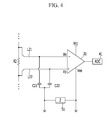
- an impedance 51 exists between the ground terminal connected with the bypass capacitors C21 and C22 and the ground terminal connected with a first power supply Vee of an amplifier 31. That is, the aforementioned two ground terminals are ground terminals that are physically different from each other to have a potential difference. Accordingly, a common mode current according to a potential difference flows, and it is difficult to detect an accurate current due to a noise component carried on the common mode current.
- aspects of the present invention include a current detecting circuit having a new structure for solving the aforementioned problems.
- aspects of embodiments of the present invention relate to a current detecting circuit, and to a current detecting circuit including a shunt resistor.
- aspects of embodiments of the present invention include a current detecting circuit having advantages of improving current accuracy.
- a current detecting circuit includes: a shunt resistor; an amplifier; a first signal line connecting a first terminal of the shunt resistor to a first input terminal of the amplifier; a second signal line connecting a second terminal of the shunt resistor to a second input terminal of the amplifier; and a third signal line connecting the second terminal of the shunt resistor to a first power supply terminal of the amplifier.
- the current detecting circuit may further include: a first capacitor connecting the first signal line to the third signal line; and a second capacitor connecting the second signal line to the third signal line.
- a pattern of the third signal line may be between a pattern of the first signal line and a pattern of the second signal line.
- An impedance of the first signal line may be matched with an impedance of the second signal line.
- An impedance of the third signal line may be matched with the impedance of the first signal line and the impedance of the second signal line.
- the impedances of the first, second, and third signal lines may be determined according to a shape of each signal line pattern.
- a capacitance of the first capacitor and a capacitance of the second capacitor may be determined according to a frequency value of an environmental noise.
- the capacitance of the first capacitor and the capacitance of the second capacitor may have a same value.
- a second power supply terminal of the amplifier may be connected to a fixed voltage source; and a voltage applied to the second power supply terminal may be larger than a voltage applied to the first power supply terminal.
- the shunt resistor may be positioned on a high current path of a battery protective circuit.
- a polarity of both voltages of the shunt resistor when the battery protective circuit is in a charge mode may be different from a polarity of the both voltages of the shunt resistor when the battery protective circuit is in a discharge mode.
- An output of the amplifier may be input to an analog to digital converter (ADC), and a current flowing in the shunt resistor may be measured according to an output of the ADC.
- ADC analog to digital converter
- the first power supply terminal may be a ground terminal.
- a battery pack according to an example embodiment of the present invention includes a battery 10 and a battery protective circuit 20.
- the battery protective circuit 20 is interposed between an anode and an external terminal P of the battery 10 and between a cathode and an external terminal N of the battery 10 to be positioned on a high current path.
- the battery protective circuit 20 includes a charging field effect transistor and a discharging field effect transistor that are connected to each other in series to control charging and discharging according to control of a controller.
- the charging field effect transistor and the discharging field effect transistor may not operate well and, as a result, when overdischarging or overcharging occurs, the controller disconnects a fuse that is a secondary protective element to block the high current path.
- a protecting operation of the battery protective circuit 20 is an example embodiment, and the present invention is not limited thereto.
- the battery protective circuit 20 of the present invention includes a shunt resistor R1 in order to perform a protection function of the battery 10. For example, in a charging mode, when the current flows to a discharging direction or a current over a predicted current flows, the current may be detected through the shunt resistor R1 and the battery protective circuit 20 may operate.
- the shunt resistor R1 may be arranged at a position to measure a current change.
- the shunt resistor R1 may be positioned on the high current path of the battery protective circuit 20.
- polarities of both voltages i.e. the voltages at each terminal of the shunt resistor
- polarities of both voltages may be changed according to a mode of the battery protective circuit 20. That is, a polarity of both voltages of the shunt resistor R1 when the battery protective circuit 20 is in the charging mode and a polarity of both voltages of the shunt resistor R1 when the battery protective circuit 20 is in the discharging mode are different from each other.
- the charging current in the charging mode and the discharging current in the discharging mode have different directions.
- the charging current in the charging mode flows in order of the external terminal P, the battery protective circuit 20, the anode of the battery 10, the cathode of the battery 10, the battery protective circuit 20, and the external terminal N.
- the discharging current in the discharging mode flows in order of the external terminal N, the battery protective circuit 20, the cathode of the battery 10, the anode of the battery 10, the battery protective circuit 20, and the external terminal P.
- An external device such as a load or a generator is connected to the external terminal P and the external terminal N.
- the shunt resistor R1 is positioned on the high current path between the cathode of the battery 10 and the external terminal N.
- the shunt resistor R1 may be positioned on the high current path between the anode of the battery 10 and the external terminal P.
- the position of the shunt resistor R1 may be determined by considering a voltage level that is applied to the first and second power supply terminals Vcc and Vee of the amplifier 30 of FIG. 2 .
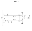
- FIG. 2 is a diagram illustrating a current detecting circuit according to the example embodiment of the present invention.
- the current detecting circuit includes the shunt resistor R1, first to third signal lines L1, L2, and L3, first and second capacitors C1 and C2, the amplifier 30, and an analog to digital converter (ADC) 40.
- ADC analog to digital converter
- the first signal line L1 connects one terminal of the shunt resistor R1 and a first input terminal Vn of the amplifier 30 to each other.
- the second signal line L2 connects the other terminal of the shunt resistor R1 and a second input terminal Vp of the amplifier 30 to each other.
- the third signal line L3 connects the other terminal of the shunt resistor R1 and the first power supply terminal Vee of the amplifier 30 to each other.
- the first power supply terminal Vee may be a ground terminal of the amplifier 30.
- the "connecting" of two elements to each other means electrically connecting the two elements to each other as long as a function to be achieved is performed.
- the “electrically connecting" of the two elements to each other means that a passive element or an active element may be interposed therebetween. That is, because another element is interposed on a predetermined path of the current detecting circuit illustrated in FIG. 2 , a person having ordinary skill in the art should recognize that certain modifications to the described embodiments may be made to have additional features or aspects, without departing from the scope of the present invention as defined by the claims.
- the first capacitor C1 connects the first signal line L1 and the third signal line L3 to each other.
- the second capacitor C2 connects the second signal line L2 and the third signal line L3 to each other.
- the first and second capacitors C1 and C2 as a bypass capacitor serve to reduce the common mode noise and the differential mode noise as described above.
- a capacitance value of the first capacitor C1 and a capacitance value of the second capacitor C2 may be the same as or similar to each other. This is to match impedance of the pattern configured by each signal line with each other, and the capacitance values of the capacitors may be different from each other according to a detailed pattern.
- the capacitance values of the first capacitor C1 and the second capacitor C2 may be determined according to a frequency value of the noise that is frequently applied in an environment where the current detecting circuit of the present invention is used.
- the first capacitor C1 and the second capacitor C2 serve to reduce the noise by bypassing an AC component of the noise. In this case, because the frequency value of the applied noise varies according to the environment where the current detecting circuit is used, the capacitance values of the first capacitor C1 and the second capacitor C2 are determined to efficiently remove the noise.
- the amplifier 30 may be an operational amplifier (OP AMP).
- the amplifier 30 may be configured by a single power or double power OP AMP.
- Input and output terminals of the amplifier 30 may vary according to a product. It is described that the amplifier 30 in the present invention includes two input terminals Vn and Vp, two power supply terminals Vcc and Vee, and one out terminal.
- the amplifier 30 amplifies and outputs a difference between the first voltage input to the first input terminal Vn and the second voltage input to the second input terminal Vp with a predetermined ratio.
- the first voltage is a voltage of one terminal of the shunt resistor Ri
- the second voltage is a voltage of the other terminal of the shunt resistor R1.
- the first input terminal Vn and the second input terminal Vp may be used to be replaced with each other.
- the third signal line L3 connects the other terminal of the shunt resistor R1 and the first power supply terminal Vee of the amplifier 30 to each other through the same voltage node. Accordingly, one terminal of each of the first and second capacitors C1 and C2 and the first power supply terminal Vee are positioned on the same voltage node. As described above, the first power supply terminal Vee may be a ground terminal of the amplifier 30.
- the ground terminal of the bypass capacitors C21 and C22 and the ground terminal of the first power supply terminal Vee are different from each other to have a potential difference. Accordingly, there is a problem in that mismatch of the potentials is amplified in the amplifier, and as a result, an undesired signal may be amplified.
- one terminal of each of the first and second capacitors C1 and C2 and the first power supply terminal Vee are positioned on physically the same voltage node, and as a result, the impedance 51 like FIG. 4 is not interposed therebetween. Accordingly, a cause of the common mode noise is removed to improve quality of the output signal.
- the second power supply terminal Vcc of the amplifier 30 may be connected to a fixed voltage source.
- the voltage applied to the second power supply terminal Vcc may be larger than the voltage applied to the first power supply terminal Vee.
- the second power supply terminal Vcc of the amplifier 30 may be connected to a node having a voltage level higher than that of the first power supply terminal Vee.
- a potential difference of the first power supply terminal Vee and the second power supply terminal Vcc may be determined by considering an output range of the amplifier 30.
- An output of the amplifier 30 is input to the ADC 40, and the current detecting circuit of the present invention may measure the current flowing in the shunt resistor R1 according to an output of the ADC 40.
- the ADC 40 is a selective configuration, and the current detecting circuit further includes an analog circuit replacing the ADC 40 to measure the current.
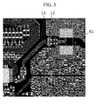
- FIG. 3 is a diagram illustrating a part of the current detecting circuit implemented on a printed circuit board (PCB) according to the example embodiment of the present invention.
- PCB printed circuit board
- the first to third signal lines L1, L2, and L3 may be patterned on the PCB.
- the impedance of the first signal line L1 and the impedance of the second signal line L2 may be matched with each other.
- the patterns of the first signal line L1 and the second signal line L2 may be the same as or similar to each other. That is, because a length, a width, and a shape of the pattern of the first signal line L1 and a length, a width, and a shape of the pattern of the second signal line L2 are the same as or similar to each other, impedance matching may be implemented.
- the third signal line L3 is patterned between the first and second signal lines L1 and L2. Accordingly, because a distance between the third signal line L3 and the first signal line L1 and a distance between the third signal line L3 and the second signal line L2 are the same as or similar to each other, impedance matching of the first and second signal lines L1 and L2 may be more easily obtained in some instances.
- the pattern of the third signal line L3 is similarly configured to the pattern of the first or second signal line L1 or L2, and as a result, the impedance of the third signal line L3 may be matched with the impedance of the first or second signal line L1 or L2.
Landscapes
- Physics & Mathematics (AREA)
- General Physics & Mathematics (AREA)
- Engineering & Computer Science (AREA)
- Power Engineering (AREA)
- Measurement Of Current Or Voltage (AREA)
Abstract
Description
- The present invention relates to a current detecting circuit.
- A shunt resistor may be arranged on a predetermined current path to measure a current.
- In order to measure a minute current difference, a resistance value of the shunt resistor may be precisely manufactured. The resistance value of the shunt resistor is generally very low, and as a result, easily influenced by a resistance value generated according to a pattern of a connected wire. Therefore, how to design the pattern of the wire is an important consideration for designers.
- Further, the current detecting circuit utilizing the shunt resistor may remove noise so as to measure a minute current change. The noise is largely divided into a common mode noise and a differential mode noise.
- The common mode noise is noise having the same phase generated for ground terminals in two signal lines. In order to remove the common mode noise, there are various methods, but as one example, there is a method of connecting bypass capacitors C21 and C22 between the ground terminals and each of two signal lines L221 and L22 (see
FIG. 4 ). The noise which is an AC component flows to the path through the bypass capacitors C21 and C22. The differential mode noise may be removed by setting a current path through the bypass capacitors C21 and C22. - However, referring to
FIG. 4 , animpedance 51 exists between the ground terminal connected with the bypass capacitors C21 and C22 and the ground terminal connected with a first power supply Vee of anamplifier 31. That is, the aforementioned two ground terminals are ground terminals that are physically different from each other to have a potential difference. Accordingly, a common mode current according to a potential difference flows, and it is difficult to detect an accurate current due to a noise component carried on the common mode current. - Further, because the position of the ground terminal connected with the bypass capacitors C21 and C22 is different from the position of the ground terminal connected to the first power supply Vee of the
amplifier 31, different noise may be transferred. - Accordingly, aspects of the present invention include a current detecting circuit having a new structure for solving the aforementioned problems.
- Aspects of embodiments of the present invention relate to a current detecting circuit, and to a current detecting circuit including a shunt resistor.
- Aspects of embodiments of the present invention include a current detecting circuit having advantages of improving current accuracy.
- According to aspects of some embodiments of the present invention, a current detecting circuit includes: a shunt resistor; an amplifier; a first signal line connecting a first terminal of the shunt resistor to a first input terminal of the amplifier; a second signal line connecting a second terminal of the shunt resistor to a second input terminal of the amplifier; and a third signal line connecting the second terminal of the shunt resistor to a first power supply terminal of the amplifier.
- The current detecting circuit may further include: a first capacitor connecting the first signal line to the third signal line; and a second capacitor connecting the second signal line to the third signal line.
- A pattern of the third signal line may be between a pattern of the first signal line and a pattern of the second signal line.
- An impedance of the first signal line may be matched with an impedance of the second signal line.
- An impedance of the third signal line may be matched with the impedance of the first signal line and the impedance of the second signal line.
- The impedances of the first, second, and third signal lines may be determined according to a shape of each signal line pattern.
- A capacitance of the first capacitor and a capacitance of the second capacitor may be determined according to a frequency value of an environmental noise.
- The capacitance of the first capacitor and the capacitance of the second capacitor may have a same value.
- A second power supply terminal of the amplifier may be connected to a fixed voltage source; and a voltage applied to the second power supply terminal may be larger than a voltage applied to the first power supply terminal.
- The shunt resistor may be positioned on a high current path of a battery protective circuit.
- A polarity of both voltages of the shunt resistor when the battery protective circuit is in a charge mode may be different from a polarity of the both voltages of the shunt resistor when the battery protective circuit is in a discharge mode.
- An output of the amplifier may be input to an analog to digital converter (ADC), and a current flowing in the shunt resistor may be measured according to an output of the ADC.
- The first power supply terminal may be a ground terminal.
- According to aspects of some embodiments of the present invention, it may be possible to provide a current detecting circuit with improved current accuracy.
- Embodiments of the invention will now be described by way of example with reference to the accompanying drawings, in which:
-
FIG. 1 is a diagram illustrating a battery pack according to an example embodiment of the present invention. -
FIG. 2 is a diagram illustrating a current detecting circuit according to the example embodiment of the present invention. -
FIG. 3 is a diagram illustrating a part of the current detecting circuit implemented on a printed circuit board (PCB) according to the example embodiment of the present invention. -
FIG. 4 is a diagram illustrating a current detecting circuit in the related art. - Referring to
FIG. 1 , a battery pack according to an example embodiment of the present invention includes abattery 10 and a batteryprotective circuit 20. - The battery
protective circuit 20 is interposed between an anode and an external terminal P of thebattery 10 and between a cathode and an external terminal N of thebattery 10 to be positioned on a high current path. - The battery
protective circuit 20 includes a charging field effect transistor and a discharging field effect transistor that are connected to each other in series to control charging and discharging according to control of a controller. The charging field effect transistor and the discharging field effect transistor may not operate well and, as a result, when overdischarging or overcharging occurs, the controller disconnects a fuse that is a secondary protective element to block the high current path. A protecting operation of the batteryprotective circuit 20 is an example embodiment, and the present invention is not limited thereto. - The battery
protective circuit 20 of the present invention includes a shunt resistor R1 in order to perform a protection function of thebattery 10. For example, in a charging mode, when the current flows to a discharging direction or a current over a predicted current flows, the current may be detected through the shunt resistor R1 and the batteryprotective circuit 20 may operate. - The shunt resistor R1 may be arranged at a position to measure a current change. The shunt resistor R1 may be positioned on the high current path of the battery
protective circuit 20. - When the shunt resistor R1 is positioned on the high current path of the battery
protective circuit 20, polarities of both voltages, i.e. the voltages at each terminal of the shunt resistor, may be changed according to a mode of the batteryprotective circuit 20. That is, a polarity of both voltages of the shunt resistor R1 when the batteryprotective circuit 20 is in the charging mode and a polarity of both voltages of the shunt resistor R1 when the batteryprotective circuit 20 is in the discharging mode are different from each other. The charging current in the charging mode and the discharging current in the discharging mode have different directions. - The charging current in the charging mode flows in order of the external terminal P, the battery
protective circuit 20, the anode of thebattery 10, the cathode of thebattery 10, the batteryprotective circuit 20, and the external terminal N. The discharging current in the discharging mode flows in order of the external terminal N, the batteryprotective circuit 20, the cathode of thebattery 10, the anode of thebattery 10, the batteryprotective circuit 20, and the external terminal P. - An external device such as a load or a generator is connected to the external terminal P and the external terminal N.
- In
FIG. 1 , the shunt resistor R1 is positioned on the high current path between the cathode of thebattery 10 and the external terminal N. As another example embodiment, the shunt resistor R1 may be positioned on the high current path between the anode of thebattery 10 and the external terminal P. The position of the shunt resistor R1 may be determined by considering a voltage level that is applied to the first and second power supply terminals Vcc and Vee of theamplifier 30 ofFIG. 2 . -
FIG. 2 is a diagram illustrating a current detecting circuit according to the example embodiment of the present invention. - Referring to
FIG. 2 , the current detecting circuit according to the example embodiment of the present invention includes the shunt resistor R1, first to third signal lines L1, L2, and L3, first and second capacitors C1 and C2, theamplifier 30, and an analog to digital converter (ADC) 40. - The first signal line L1 connects one terminal of the shunt resistor R1 and a first input terminal Vn of the
amplifier 30 to each other. The second signal line L2 connects the other terminal of the shunt resistor R1 and a second input terminal Vp of theamplifier 30 to each other. The third signal line L3 connects the other terminal of the shunt resistor R1 and the first power supply terminal Vee of theamplifier 30 to each other. In this case, the first power supply terminal Vee may be a ground terminal of theamplifier 30. - Hereinafter, in the present invention, the "connecting" of two elements to each other means electrically connecting the two elements to each other as long as a function to be achieved is performed. The "electrically connecting" of the two elements to each other means that a passive element or an active element may be interposed therebetween. That is, because another element is interposed on a predetermined path of the current detecting circuit illustrated in
FIG. 2 , a person having ordinary skill in the art should recognize that certain modifications to the described embodiments may be made to have additional features or aspects, without departing from the scope of the present invention as defined by the claims. - The first capacitor C1 connects the first signal line L1 and the third signal line L3 to each other. The second capacitor C2 connects the second signal line L2 and the third signal line L3 to each other.
- The first and second capacitors C1 and C2 as a bypass capacitor serve to reduce the common mode noise and the differential mode noise as described above.
- As one example embodiment, a capacitance value of the first capacitor C1 and a capacitance value of the second capacitor C2 may be the same as or similar to each other. This is to match impedance of the pattern configured by each signal line with each other, and the capacitance values of the capacitors may be different from each other according to a detailed pattern.
- The capacitance values of the first capacitor C1 and the second capacitor C2 may be determined according to a frequency value of the noise that is frequently applied in an environment where the current detecting circuit of the present invention is used. The first capacitor C1 and the second capacitor C2 serve to reduce the noise by bypassing an AC component of the noise. In this case, because the frequency value of the applied noise varies according to the environment where the current detecting circuit is used, the capacitance values of the first capacitor C1 and the second capacitor C2 are determined to efficiently remove the noise.
- The
amplifier 30 may be an operational amplifier (OP AMP). Theamplifier 30 may be configured by a single power or double power OP AMP. Input and output terminals of theamplifier 30 may vary according to a product. It is described that theamplifier 30 in the present invention includes two input terminals Vn and Vp, two power supply terminals Vcc and Vee, and one out terminal. - The
amplifier 30 amplifies and outputs a difference between the first voltage input to the first input terminal Vn and the second voltage input to the second input terminal Vp with a predetermined ratio. In the example embodiment, the first voltage is a voltage of one terminal of the shunt resistor Ri, and the second voltage is a voltage of the other terminal of the shunt resistor R1. The first input terminal Vn and the second input terminal Vp may be used to be replaced with each other. - The third signal line L3 connects the other terminal of the shunt resistor R1 and the first power supply terminal Vee of the
amplifier 30 to each other through the same voltage node. Accordingly, one terminal of each of the first and second capacitors C1 and C2 and the first power supply terminal Vee are positioned on the same voltage node. As described above, the first power supply terminal Vee may be a ground terminal of theamplifier 30. - As described above, referring to
FIG. 4 , in a current protective circuit in the related art, the ground terminal of the bypass capacitors C21 and C22 and the ground terminal of the first power supply terminal Vee are different from each other to have a potential difference. Accordingly, there is a problem in that mismatch of the potentials is amplified in the amplifier, and as a result, an undesired signal may be amplified. - However, in the present invention, one terminal of each of the first and second capacitors C1 and C2 and the first power supply terminal Vee are positioned on physically the same voltage node, and as a result, the
impedance 51 likeFIG. 4 is not interposed therebetween. Accordingly, a cause of the common mode noise is removed to improve quality of the output signal. - The second power supply terminal Vcc of the
amplifier 30 may be connected to a fixed voltage source. In this case, the voltage applied to the second power supply terminal Vcc may be larger than the voltage applied to the first power supply terminal Vee. - As another example embodiment, the second power supply terminal Vcc of the
amplifier 30 may be connected to a node having a voltage level higher than that of the first power supply terminal Vee. A potential difference of the first power supply terminal Vee and the second power supply terminal Vcc may be determined by considering an output range of theamplifier 30. - An output of the
amplifier 30 is input to theADC 40, and the current detecting circuit of the present invention may measure the current flowing in the shunt resistor R1 according to an output of theADC 40. TheADC 40 is a selective configuration, and the current detecting circuit further includes an analog circuit replacing theADC 40 to measure the current. -
FIG. 3 is a diagram illustrating a part of the current detecting circuit implemented on a printed circuit board (PCB) according to the example embodiment of the present invention. - Referring to
FIG. 3 , the first to third signal lines L1, L2, and L3 may be patterned on the PCB. - The impedance of the first signal line L1 and the impedance of the second signal line L2 may be matched with each other. When the first signal line L1 and the second signal line L2 are configured by (or formed of) the same material (for example, copper), the patterns of the first signal line L1 and the second signal line L2 may be the same as or similar to each other. That is, because a length, a width, and a shape of the pattern of the first signal line L1 and a length, a width, and a shape of the pattern of the second signal line L2 are the same as or similar to each other, impedance matching may be implemented.
- The third signal line L3 is patterned between the first and second signal lines L1 and L2. Accordingly, because a distance between the third signal line L3 and the first signal line L1 and a distance between the third signal line L3 and the second signal line L2 are the same as or similar to each other, impedance matching of the first and second signal lines L1 and L2 may be more easily obtained in some instances.
- In this case, the pattern of the third signal line L3 is similarly configured to the pattern of the first or second signal line L1 or L2, and as a result, the impedance of the third signal line L3 may be matched with the impedance of the first or second signal line L1 or L2.
- While this invention has been described in connection with what are presently considered to be practical example embodiments, it is to be understood that the invention is not limited to the disclosed embodiments, but, on the contrary, is intended to cover various modifications and equivalent arrangements included within the scope of the appended claims.
Claims (13)
- A current detecting circuit, comprising:a shunt resistor;an amplifier;a first signal line connecting a first terminal of the shunt resistor to a first input terminal of the amplifier;a second signal line connecting a second terminal of the shunt resistor to a second input terminal of the amplifier; anda third signal line connecting the second terminal of the shunt resistor to a first power supply terminal of the amplifier.
- The current detecting circuit of claim 1, further comprising:a first capacitor connecting the first signal line to the third signal line; anda second capacitor connecting the second signal line to the third signal line.
- The current detecting circuit of claim 1 or 2, wherein:a pattern of the third signal line is arranged between a pattern of the first signal line and a pattern of the second signal line.
- The current detecting circuit of any one of the preceding claims, wherein:an impedance of the first signal line is matched with an impedance of the second signal line.
- The current detecting circuit of claim 4, wherein:an impedance of the third signal line is matched with the impedance of the first signal line and the impedance of the second signal line.
- The current detecting circuit of any one of the preceding claims, wherein:the impedances of the first, second, and third signal lines are determined according to the shape of each signal line pattern.
- The current detecting circuit of any one of claims 3 to 6 when dependent on claim 2, wherein:a capacitance of the first capacitor and a capacitance of the second capacitor are determined according to a frequency value of an environmental noise.
- The current detecting circuit of claim 7, wherein:the capacitance of the first capacitor and the capacitance of the second capacitor have the same value.
- The current detecting circuit of any one of claims 4 to 8 when dependent on claim 3, wherein:a second power supply terminal of the amplifier is connected to a fixed voltage source; anda voltage applied to the second power supply terminal is larger than a voltage applied to the first power supply terminal.
- The current detecting circuit of any one of the preceding claims, wherein:the shunt resistor is positioned on a high current path of a battery protective circuit.
- The current detecting circuit of claim 10, wherein:a polarity of both voltages of the shunt resistor when the battery protective circuit is in a charge mode is different from a polarity of the both voltages of the shunt resistor when the battery protective circuit is in a discharge mode.
- The current detecting circuit of any one of claims 4 to 9 when dependent on claim 3, wherein:an output of the amplifier is input to an analog to digital converter ADC, anda current flowing in the shunt resistor is measured according to an output of the ADC.
- The current detecting circuit of any one of the preceding claims, wherein:the first power supply terminal is a ground terminal.
Applications Claiming Priority (1)
| Application Number | Priority Date | Filing Date | Title |
|---|---|---|---|
| KR1020150080860A KR102345505B1 (en) | 2015-06-08 | 2015-06-08 | Current detecting circuit |
Publications (2)
| Publication Number | Publication Date |
|---|---|
| EP3104182A1 true EP3104182A1 (en) | 2016-12-14 |
| EP3104182B1 EP3104182B1 (en) | 2020-03-11 |
Family
ID=56117556
Family Applications (1)
| Application Number | Title | Priority Date | Filing Date |
|---|---|---|---|
| EP16173534.5A Active EP3104182B1 (en) | 2015-06-08 | 2016-06-08 | Current detecting circuit |
Country Status (4)
| Country | Link |
|---|---|
| US (1) | US20160356825A1 (en) |
| EP (1) | EP3104182B1 (en) |
| KR (1) | KR102345505B1 (en) |
| CN (1) | CN106249037B (en) |
Families Citing this family (7)
| Publication number | Priority date | Publication date | Assignee | Title |
|---|---|---|---|---|
| JP7098289B2 (en) * | 2017-08-29 | 2022-07-11 | Koa株式会社 | Current measuring device |
| US11899043B2 (en) * | 2019-04-26 | 2024-02-13 | Autonetworks Technologies, Ltd. | Current detection apparatus and power supply control apparatus |
| US11333685B1 (en) | 2020-02-13 | 2022-05-17 | Sendyne Corporation | Functional safety of measurements |
| US20250012833A1 (en) * | 2021-11-26 | 2025-01-09 | Mitsubishi Electric Corporation | Detection circuit |
| WO2023244518A1 (en) * | 2022-06-14 | 2023-12-21 | Kyocera Senco Industrial Tools, Inc. | Battery adapter for power tools |
| KR102854441B1 (en) * | 2022-11-28 | 2025-09-02 | 주식회사 현대케피코 | Engine control apparatus having dark current measuring function and dark current mearusing method thereof |
| CN119450917A (en) * | 2023-07-31 | 2025-02-14 | 台达电子工业股份有限公司 | Circuit board module and electronic device using the circuit board module |
Citations (8)
| Publication number | Priority date | Publication date | Assignee | Title |
|---|---|---|---|---|
| US5438252A (en) * | 1991-11-25 | 1995-08-01 | Societe Anonyme Dite: Saft | Power supply control module for a battery control system of an appliance, and a battery equipped with such a module |
| US5945853A (en) * | 1997-04-24 | 1999-08-31 | Sanyo Electric Co., Ltd. | Current sensing circuit with automatic offset compensation |
| US20030025514A1 (en) * | 2001-07-26 | 2003-02-06 | Benes Michael J. | Multiple range current measurement system with low power dissipation, fast settling time, and low common mode voltage error |
| WO2005006392A2 (en) * | 2003-06-24 | 2005-01-20 | Atmel Corporation | Low voltage circuit for interfacing with high voltage analog signals |
| WO2007028960A1 (en) * | 2005-09-07 | 2007-03-15 | Trw Limited | Current measurement circuit and method of diagnosing faults in same |
| EP2244319A1 (en) * | 2009-04-24 | 2010-10-27 | Sanyo Electric Co., Ltd. | Battery module, battery system and electric vehicle |
| US20130307511A1 (en) * | 2011-02-11 | 2013-11-21 | Ian Douglas De Vries | Hysteretic current mode controller for a bidirectional converter with lossless inductor current sensing |
| US20150077091A1 (en) * | 2011-03-01 | 2015-03-19 | Sendyne Corporation | Current sensor |
Family Cites Families (11)
| Publication number | Priority date | Publication date | Assignee | Title |
|---|---|---|---|---|
| JPH07306883A (en) * | 1994-05-12 | 1995-11-21 | Fujitsu Ltd | Pattern evaluation support device |
| US6946845B2 (en) * | 2002-05-14 | 2005-09-20 | Isabellenhutte Heusler Gmbh Kg | Current, voltage and temperature measuring circuit |
| US8278876B2 (en) * | 2005-03-07 | 2012-10-02 | O2Micro, Inc. | Battery pack current monitoring |
| JP4531608B2 (en) * | 2005-03-30 | 2010-08-25 | ルネサスエレクトロニクス株式会社 | Battery voltage measuring device |
| JP5469813B2 (en) * | 2008-01-29 | 2014-04-16 | 株式会社日立製作所 | Battery system for vehicles |
| EP2120485B1 (en) * | 2008-04-28 | 2014-10-08 | Harman Becker Automotive Systems GmbH | Load detection |
| US8264216B2 (en) * | 2010-09-21 | 2012-09-11 | Sendyne Corp. | High-accuracy low-power current sensor with large dynamic range |
| CN102231549B (en) * | 2011-07-04 | 2013-12-11 | 重庆长安汽车股份有限公司 | Battery management chip |
| JP5348259B2 (en) * | 2012-02-02 | 2013-11-20 | 横河電機株式会社 | Insulation circuit and communication equipment |
| JP6237982B2 (en) * | 2013-04-23 | 2017-11-29 | セイコーエプソン株式会社 | Physical quantity sensor, electronic device and moving object |
| US9208764B2 (en) * | 2013-07-05 | 2015-12-08 | Google Inc. | Methods and devices for determining media files based on activity levels |
-
2015
- 2015-06-08 KR KR1020150080860A patent/KR102345505B1/en active Active
-
2016
- 2016-05-17 US US15/157,168 patent/US20160356825A1/en not_active Abandoned
- 2016-06-08 EP EP16173534.5A patent/EP3104182B1/en active Active
- 2016-06-08 CN CN201610404415.4A patent/CN106249037B/en active Active
Patent Citations (8)
| Publication number | Priority date | Publication date | Assignee | Title |
|---|---|---|---|---|
| US5438252A (en) * | 1991-11-25 | 1995-08-01 | Societe Anonyme Dite: Saft | Power supply control module for a battery control system of an appliance, and a battery equipped with such a module |
| US5945853A (en) * | 1997-04-24 | 1999-08-31 | Sanyo Electric Co., Ltd. | Current sensing circuit with automatic offset compensation |
| US20030025514A1 (en) * | 2001-07-26 | 2003-02-06 | Benes Michael J. | Multiple range current measurement system with low power dissipation, fast settling time, and low common mode voltage error |
| WO2005006392A2 (en) * | 2003-06-24 | 2005-01-20 | Atmel Corporation | Low voltage circuit for interfacing with high voltage analog signals |
| WO2007028960A1 (en) * | 2005-09-07 | 2007-03-15 | Trw Limited | Current measurement circuit and method of diagnosing faults in same |
| EP2244319A1 (en) * | 2009-04-24 | 2010-10-27 | Sanyo Electric Co., Ltd. | Battery module, battery system and electric vehicle |
| US20130307511A1 (en) * | 2011-02-11 | 2013-11-21 | Ian Douglas De Vries | Hysteretic current mode controller for a bidirectional converter with lossless inductor current sensing |
| US20150077091A1 (en) * | 2011-03-01 | 2015-03-19 | Sendyne Corporation | Current sensor |
Non-Patent Citations (2)
| Title |
|---|
| STEPHEN ENGLAND: "High Side Resistive Shunt Current Sensing Using Current Shunt Monitors From Texas Instruments Table of Contents", 4 April 2011 (2011-04-04), XP055303391, Retrieved from the Internet <URL:http://www.egr.msu.edu/classes/ece480/capstone/spring11/group05/documents/app_note_s11_dt5_stephen.pdf> [retrieved on 20160916] * |
| TIM REGAN ET AL: "Application Note 105: Current Sense Circuit Collection Making Sense Of Current", INTERNET CITATION, 1 December 2005 (2005-12-01), pages 1 - 118, XP002732091, Retrieved from the Internet <URL:http://cds.linear.com/docs/en/application-note/an105fa.pdf> [retrieved on 20141105] * |
Also Published As
| Publication number | Publication date |
|---|---|
| CN106249037B (en) | 2020-11-20 |
| US20160356825A1 (en) | 2016-12-08 |
| KR102345505B1 (en) | 2021-12-29 |
| EP3104182B1 (en) | 2020-03-11 |
| KR20160144262A (en) | 2016-12-16 |
| CN106249037A (en) | 2016-12-21 |
Similar Documents
| Publication | Publication Date | Title |
|---|---|---|
| EP3104182B1 (en) | Current detecting circuit | |
| JP4241787B2 (en) | Total battery voltage detection and leak detection device | |
| TWI761549B (en) | Secondary battery protection circuit, secondary battery protection integrated circuit and battery pack | |
| US8786289B2 (en) | Method and semiconductor device for monitoring battery voltages | |
| US9658270B2 (en) | Inspection method of sensor device and sensor device | |
| EP3516404B1 (en) | Current sense amplifier architecture and level shifter | |
| JP2002296316A (en) | Leakage detecting circuit for power-supply device | |
| US9812743B2 (en) | Battery state monitoring circuit and battery device | |
| US9366730B2 (en) | Battery voltage detector circuit | |
| US7446554B2 (en) | Direct current measuring apparatus and limiting circuit | |
| US20170315181A1 (en) | Integrated circuit with built-in status monitoring unit and power supply device provided with said integrated circuit | |
| CN106936175B (en) | Charge and discharge control circuit and battery device | |
| US10317248B2 (en) | Multiple-distance proximity sensor systems | |
| KR102365630B1 (en) | Apparatus and method for detecting ovr current | |
| KR20150110717A (en) | Voltage measurement device | |
| JP2007333529A (en) | Insulation resistance measuring apparatus, leakage current measuring apparatus, insulation resistance measurement method and leakage current measurement method | |
| JP6444772B2 (en) | Voltage detection device, voltage detection method, and battery pack system | |
| EP3327454A1 (en) | Battery system with a shared cell supervision circuit unit | |
| EP4039323B1 (en) | Detection circuit for a nerve stimulator | |
| JP6714860B2 (en) | Measurement module | |
| JP2011507477A (en) | Integrated circuit having a DC-DC converter | |
| JP2005172796A (en) | Current-voltage conversion circuit | |
| TW201902018A (en) | Charge and discharge control circuit and battery device having the same | |
| JP7120129B2 (en) | battery monitor | |
| JPWO2018235457A1 (en) | Battery system monitoring device and battery pack |
Legal Events
| Date | Code | Title | Description |
|---|---|---|---|
| PUAI | Public reference made under article 153(3) epc to a published international application that has entered the european phase |
Free format text: ORIGINAL CODE: 0009012 |
|
| STAA | Information on the status of an ep patent application or granted ep patent |
Free format text: STATUS: THE APPLICATION HAS BEEN PUBLISHED |
|
| AK | Designated contracting states |
Kind code of ref document: A1 Designated state(s): AL AT BE BG CH CY CZ DE DK EE ES FI FR GB GR HR HU IE IS IT LI LT LU LV MC MK MT NL NO PL PT RO RS SE SI SK SM TR |
|
| AX | Request for extension of the european patent |
Extension state: BA ME |
|
| STAA | Information on the status of an ep patent application or granted ep patent |
Free format text: STATUS: REQUEST FOR EXAMINATION WAS MADE |
|
| 17P | Request for examination filed |
Effective date: 20170530 |
|
| RBV | Designated contracting states (corrected) |
Designated state(s): AL AT BE BG CH CY CZ DE DK EE ES FI FR GB GR HR HU IE IS IT LI LT LU LV MC MK MT NL NO PL PT RO RS SE SI SK SM TR |
|
| STAA | Information on the status of an ep patent application or granted ep patent |
Free format text: STATUS: EXAMINATION IS IN PROGRESS |
|
| 17Q | First examination report despatched |
Effective date: 20180508 |
|
| RIC1 | Information provided on ipc code assigned before grant |
Ipc: G01R 31/36 20190101ALN20190919BHEP Ipc: H03F 1/26 20060101ALI20190919BHEP Ipc: H03F 3/45 20060101ALI20190919BHEP Ipc: H05K 1/02 20060101ALI20190919BHEP Ipc: H02H 7/18 20060101ALN20190919BHEP Ipc: G01R 15/14 20060101AFI20190919BHEP Ipc: G01R 1/20 20060101ALN20190919BHEP |
|
| GRAP | Despatch of communication of intention to grant a patent |
Free format text: ORIGINAL CODE: EPIDOSNIGR1 |
|
| STAA | Information on the status of an ep patent application or granted ep patent |
Free format text: STATUS: GRANT OF PATENT IS INTENDED |
|
| INTG | Intention to grant announced |
Effective date: 20191104 |
|
| GRAS | Grant fee paid |
Free format text: ORIGINAL CODE: EPIDOSNIGR3 |
|
| GRAA | (expected) grant |
Free format text: ORIGINAL CODE: 0009210 |
|
| STAA | Information on the status of an ep patent application or granted ep patent |
Free format text: STATUS: THE PATENT HAS BEEN GRANTED |
|
| AK | Designated contracting states |
Kind code of ref document: B1 Designated state(s): AL AT BE BG CH CY CZ DE DK EE ES FI FR GB GR HR HU IE IS IT LI LT LU LV MC MK MT NL NO PL PT RO RS SE SI SK SM TR |
|
| REG | Reference to a national code |
Ref country code: GB Ref legal event code: FG4D |
|
| REG | Reference to a national code |
Ref country code: CH Ref legal event code: EP |
|
| REG | Reference to a national code |
Ref country code: AT Ref legal event code: REF Ref document number: 1243808 Country of ref document: AT Kind code of ref document: T Effective date: 20200315 |
|
| REG | Reference to a national code |
Ref country code: IE Ref legal event code: FG4D |
|
| REG | Reference to a national code |
Ref country code: DE Ref legal event code: R096 Ref document number: 602016031366 Country of ref document: DE |
|
| PG25 | Lapsed in a contracting state [announced via postgrant information from national office to epo] |
Ref country code: FI Free format text: LAPSE BECAUSE OF FAILURE TO SUBMIT A TRANSLATION OF THE DESCRIPTION OR TO PAY THE FEE WITHIN THE PRESCRIBED TIME-LIMIT Effective date: 20200311 Ref country code: NO Free format text: LAPSE BECAUSE OF FAILURE TO SUBMIT A TRANSLATION OF THE DESCRIPTION OR TO PAY THE FEE WITHIN THE PRESCRIBED TIME-LIMIT Effective date: 20200611 Ref country code: RS Free format text: LAPSE BECAUSE OF FAILURE TO SUBMIT A TRANSLATION OF THE DESCRIPTION OR TO PAY THE FEE WITHIN THE PRESCRIBED TIME-LIMIT Effective date: 20200311 |
|
| REG | Reference to a national code |
Ref country code: NL Ref legal event code: MP Effective date: 20200311 |
|
| PG25 | Lapsed in a contracting state [announced via postgrant information from national office to epo] |
Ref country code: BG Free format text: LAPSE BECAUSE OF FAILURE TO SUBMIT A TRANSLATION OF THE DESCRIPTION OR TO PAY THE FEE WITHIN THE PRESCRIBED TIME-LIMIT Effective date: 20200611 Ref country code: GR Free format text: LAPSE BECAUSE OF FAILURE TO SUBMIT A TRANSLATION OF THE DESCRIPTION OR TO PAY THE FEE WITHIN THE PRESCRIBED TIME-LIMIT Effective date: 20200612 Ref country code: LV Free format text: LAPSE BECAUSE OF FAILURE TO SUBMIT A TRANSLATION OF THE DESCRIPTION OR TO PAY THE FEE WITHIN THE PRESCRIBED TIME-LIMIT Effective date: 20200311 Ref country code: SE Free format text: LAPSE BECAUSE OF FAILURE TO SUBMIT A TRANSLATION OF THE DESCRIPTION OR TO PAY THE FEE WITHIN THE PRESCRIBED TIME-LIMIT Effective date: 20200311 Ref country code: HR Free format text: LAPSE BECAUSE OF FAILURE TO SUBMIT A TRANSLATION OF THE DESCRIPTION OR TO PAY THE FEE WITHIN THE PRESCRIBED TIME-LIMIT Effective date: 20200311 |
|
| REG | Reference to a national code |
Ref country code: LT Ref legal event code: MG4D |
|
| PG25 | Lapsed in a contracting state [announced via postgrant information from national office to epo] |
Ref country code: NL Free format text: LAPSE BECAUSE OF FAILURE TO SUBMIT A TRANSLATION OF THE DESCRIPTION OR TO PAY THE FEE WITHIN THE PRESCRIBED TIME-LIMIT Effective date: 20200311 |
|
| PG25 | Lapsed in a contracting state [announced via postgrant information from national office to epo] |
Ref country code: PT Free format text: LAPSE BECAUSE OF FAILURE TO SUBMIT A TRANSLATION OF THE DESCRIPTION OR TO PAY THE FEE WITHIN THE PRESCRIBED TIME-LIMIT Effective date: 20200805 Ref country code: LT Free format text: LAPSE BECAUSE OF FAILURE TO SUBMIT A TRANSLATION OF THE DESCRIPTION OR TO PAY THE FEE WITHIN THE PRESCRIBED TIME-LIMIT Effective date: 20200311 Ref country code: CZ Free format text: LAPSE BECAUSE OF FAILURE TO SUBMIT A TRANSLATION OF THE DESCRIPTION OR TO PAY THE FEE WITHIN THE PRESCRIBED TIME-LIMIT Effective date: 20200311 Ref country code: SK Free format text: LAPSE BECAUSE OF FAILURE TO SUBMIT A TRANSLATION OF THE DESCRIPTION OR TO PAY THE FEE WITHIN THE PRESCRIBED TIME-LIMIT Effective date: 20200311 Ref country code: IS Free format text: LAPSE BECAUSE OF FAILURE TO SUBMIT A TRANSLATION OF THE DESCRIPTION OR TO PAY THE FEE WITHIN THE PRESCRIBED TIME-LIMIT Effective date: 20200711 Ref country code: RO Free format text: LAPSE BECAUSE OF FAILURE TO SUBMIT A TRANSLATION OF THE DESCRIPTION OR TO PAY THE FEE WITHIN THE PRESCRIBED TIME-LIMIT Effective date: 20200311 Ref country code: SM Free format text: LAPSE BECAUSE OF FAILURE TO SUBMIT A TRANSLATION OF THE DESCRIPTION OR TO PAY THE FEE WITHIN THE PRESCRIBED TIME-LIMIT Effective date: 20200311 Ref country code: EE Free format text: LAPSE BECAUSE OF FAILURE TO SUBMIT A TRANSLATION OF THE DESCRIPTION OR TO PAY THE FEE WITHIN THE PRESCRIBED TIME-LIMIT Effective date: 20200311 |
|
| REG | Reference to a national code |
Ref country code: DE Ref legal event code: R097 Ref document number: 602016031366 Country of ref document: DE |
|
| PLBE | No opposition filed within time limit |
Free format text: ORIGINAL CODE: 0009261 |
|
| STAA | Information on the status of an ep patent application or granted ep patent |
Free format text: STATUS: NO OPPOSITION FILED WITHIN TIME LIMIT |
|
| PG25 | Lapsed in a contracting state [announced via postgrant information from national office to epo] |
Ref country code: IT Free format text: LAPSE BECAUSE OF FAILURE TO SUBMIT A TRANSLATION OF THE DESCRIPTION OR TO PAY THE FEE WITHIN THE PRESCRIBED TIME-LIMIT Effective date: 20200311 Ref country code: MC Free format text: LAPSE BECAUSE OF FAILURE TO SUBMIT A TRANSLATION OF THE DESCRIPTION OR TO PAY THE FEE WITHIN THE PRESCRIBED TIME-LIMIT Effective date: 20200311 Ref country code: DK Free format text: LAPSE BECAUSE OF FAILURE TO SUBMIT A TRANSLATION OF THE DESCRIPTION OR TO PAY THE FEE WITHIN THE PRESCRIBED TIME-LIMIT Effective date: 20200311 Ref country code: ES Free format text: LAPSE BECAUSE OF FAILURE TO SUBMIT A TRANSLATION OF THE DESCRIPTION OR TO PAY THE FEE WITHIN THE PRESCRIBED TIME-LIMIT Effective date: 20200311 |
|
| REG | Reference to a national code |
Ref country code: CH Ref legal event code: PL |
|
| 26N | No opposition filed |
Effective date: 20201214 |
|
| PG25 | Lapsed in a contracting state [announced via postgrant information from national office to epo] |
Ref country code: SI Free format text: LAPSE BECAUSE OF FAILURE TO SUBMIT A TRANSLATION OF THE DESCRIPTION OR TO PAY THE FEE WITHIN THE PRESCRIBED TIME-LIMIT Effective date: 20200311 Ref country code: PL Free format text: LAPSE BECAUSE OF FAILURE TO SUBMIT A TRANSLATION OF THE DESCRIPTION OR TO PAY THE FEE WITHIN THE PRESCRIBED TIME-LIMIT Effective date: 20200311 |
|
| PG25 | Lapsed in a contracting state [announced via postgrant information from national office to epo] |
Ref country code: LU Free format text: LAPSE BECAUSE OF NON-PAYMENT OF DUE FEES Effective date: 20200608 |
|
| REG | Reference to a national code |
Ref country code: BE Ref legal event code: MM Effective date: 20200630 |
|
| PG25 | Lapsed in a contracting state [announced via postgrant information from national office to epo] |
Ref country code: CH Free format text: LAPSE BECAUSE OF NON-PAYMENT OF DUE FEES Effective date: 20200630 Ref country code: LI Free format text: LAPSE BECAUSE OF NON-PAYMENT OF DUE FEES Effective date: 20200630 Ref country code: IE Free format text: LAPSE BECAUSE OF NON-PAYMENT OF DUE FEES Effective date: 20200608 |
|
| PG25 | Lapsed in a contracting state [announced via postgrant information from national office to epo] |
Ref country code: BE Free format text: LAPSE BECAUSE OF NON-PAYMENT OF DUE FEES Effective date: 20200630 |
|
| REG | Reference to a national code |
Ref country code: AT Ref legal event code: UEP Ref document number: 1243808 Country of ref document: AT Kind code of ref document: T Effective date: 20200311 |
|
| PG25 | Lapsed in a contracting state [announced via postgrant information from national office to epo] |
Ref country code: TR Free format text: LAPSE BECAUSE OF FAILURE TO SUBMIT A TRANSLATION OF THE DESCRIPTION OR TO PAY THE FEE WITHIN THE PRESCRIBED TIME-LIMIT Effective date: 20200311 Ref country code: MT Free format text: LAPSE BECAUSE OF FAILURE TO SUBMIT A TRANSLATION OF THE DESCRIPTION OR TO PAY THE FEE WITHIN THE PRESCRIBED TIME-LIMIT Effective date: 20200311 Ref country code: CY Free format text: LAPSE BECAUSE OF FAILURE TO SUBMIT A TRANSLATION OF THE DESCRIPTION OR TO PAY THE FEE WITHIN THE PRESCRIBED TIME-LIMIT Effective date: 20200311 |
|
| PG25 | Lapsed in a contracting state [announced via postgrant information from national office to epo] |
Ref country code: MK Free format text: LAPSE BECAUSE OF FAILURE TO SUBMIT A TRANSLATION OF THE DESCRIPTION OR TO PAY THE FEE WITHIN THE PRESCRIBED TIME-LIMIT Effective date: 20200311 Ref country code: AL Free format text: LAPSE BECAUSE OF FAILURE TO SUBMIT A TRANSLATION OF THE DESCRIPTION OR TO PAY THE FEE WITHIN THE PRESCRIBED TIME-LIMIT Effective date: 20200311 |
|
| P01 | Opt-out of the competence of the unified patent court (upc) registered |
Effective date: 20230528 |
|
| PGFP | Annual fee paid to national office [announced via postgrant information from national office to epo] |
Ref country code: DE Payment date: 20250604 Year of fee payment: 10 |
|
| PGFP | Annual fee paid to national office [announced via postgrant information from national office to epo] |
Ref country code: GB Payment date: 20250529 Year of fee payment: 10 |
|
| PGFP | Annual fee paid to national office [announced via postgrant information from national office to epo] |
Ref country code: FR Payment date: 20250610 Year of fee payment: 10 |
|
| PGFP | Annual fee paid to national office [announced via postgrant information from national office to epo] |
Ref country code: AT Payment date: 20250610 Year of fee payment: 10 |