EP3104072B1 - Light source module and planar light source device including the same - Google Patents
Light source module and planar light source device including the same Download PDFInfo
- Publication number
- EP3104072B1 EP3104072B1 EP16173729.1A EP16173729A EP3104072B1 EP 3104072 B1 EP3104072 B1 EP 3104072B1 EP 16173729 A EP16173729 A EP 16173729A EP 3104072 B1 EP3104072 B1 EP 3104072B1
- Authority
- EP
- European Patent Office
- Prior art keywords
- light
- reflective
- light source
- guide plate
- circuit board
- Prior art date
- Legal status (The legal status is an assumption and is not a legal conclusion. Google has not performed a legal analysis and makes no representation as to the accuracy of the status listed.)
- Active
Links
Images






Classifications
-
- F—MECHANICAL ENGINEERING; LIGHTING; HEATING; WEAPONS; BLASTING
- F21—LIGHTING
- F21K—NON-ELECTRIC LIGHT SOURCES USING LUMINESCENCE; LIGHT SOURCES USING ELECTROCHEMILUMINESCENCE; LIGHT SOURCES USING CHARGES OF COMBUSTIBLE MATERIAL; LIGHT SOURCES USING SEMICONDUCTOR DEVICES AS LIGHT-GENERATING ELEMENTS; LIGHT SOURCES NOT OTHERWISE PROVIDED FOR
- F21K9/00—Light sources using semiconductor devices as light-generating elements, e.g. using light-emitting diodes [LED] or lasers
- F21K9/60—Optical arrangements integrated in the light source, e.g. for improving the colour rendering index or the light extraction
- F21K9/61—Optical arrangements integrated in the light source, e.g. for improving the colour rendering index or the light extraction using light guides
-
- G—PHYSICS
- G02—OPTICS
- G02B—OPTICAL ELEMENTS, SYSTEMS OR APPARATUS
- G02B6/00—Light guides; Structural details of arrangements comprising light guides and other optical elements, e.g. couplings
- G02B6/0001—Light guides; Structural details of arrangements comprising light guides and other optical elements, e.g. couplings specially adapted for lighting devices or systems
- G02B6/0011—Light guides; Structural details of arrangements comprising light guides and other optical elements, e.g. couplings specially adapted for lighting devices or systems the light guides being planar or of plate-like form
- G02B6/0013—Means for improving the coupling-in of light from the light source into the light guide
- G02B6/0023—Means for improving the coupling-in of light from the light source into the light guide provided by one optical element, or plurality thereof, placed between the light guide and the light source, or around the light source
- G02B6/0031—Reflecting element, sheet or layer
-
- G—PHYSICS
- G02—OPTICS
- G02F—OPTICAL DEVICES OR ARRANGEMENTS FOR THE CONTROL OF LIGHT BY MODIFICATION OF THE OPTICAL PROPERTIES OF THE MEDIA OF THE ELEMENTS INVOLVED THEREIN; NON-LINEAR OPTICS; FREQUENCY-CHANGING OF LIGHT; OPTICAL LOGIC ELEMENTS; OPTICAL ANALOGUE/DIGITAL CONVERTERS
- G02F1/00—Devices or arrangements for the control of the intensity, colour, phase, polarisation or direction of light arriving from an independent light source, e.g. switching, gating or modulating; Non-linear optics
- G02F1/01—Devices or arrangements for the control of the intensity, colour, phase, polarisation or direction of light arriving from an independent light source, e.g. switching, gating or modulating; Non-linear optics for the control of the intensity, phase, polarisation or colour
- G02F1/13—Devices or arrangements for the control of the intensity, colour, phase, polarisation or direction of light arriving from an independent light source, e.g. switching, gating or modulating; Non-linear optics for the control of the intensity, phase, polarisation or colour based on liquid crystals, e.g. single liquid crystal display cells
- G02F1/133—Constructional arrangements; Operation of liquid crystal cells; Circuit arrangements
- G02F1/1333—Constructional arrangements; Manufacturing methods
- G02F1/1335—Structural association of cells with optical devices, e.g. polarisers or reflectors
- G02F1/1336—Illuminating devices
- G02F1/133615—Edge-illuminating devices, i.e. illuminating from the side
-
- F—MECHANICAL ENGINEERING; LIGHTING; HEATING; WEAPONS; BLASTING
- F21—LIGHTING
- F21K—NON-ELECTRIC LIGHT SOURCES USING LUMINESCENCE; LIGHT SOURCES USING ELECTROCHEMILUMINESCENCE; LIGHT SOURCES USING CHARGES OF COMBUSTIBLE MATERIAL; LIGHT SOURCES USING SEMICONDUCTOR DEVICES AS LIGHT-GENERATING ELEMENTS; LIGHT SOURCES NOT OTHERWISE PROVIDED FOR
- F21K9/00—Light sources using semiconductor devices as light-generating elements, e.g. using light-emitting diodes [LED] or lasers
- F21K9/60—Optical arrangements integrated in the light source, e.g. for improving the colour rendering index or the light extraction
- F21K9/62—Optical arrangements integrated in the light source, e.g. for improving the colour rendering index or the light extraction using mixing chambers, e.g. housings with reflective walls
-
- F—MECHANICAL ENGINEERING; LIGHTING; HEATING; WEAPONS; BLASTING
- F21—LIGHTING
- F21S—NON-PORTABLE LIGHTING DEVICES; SYSTEMS THEREOF; VEHICLE LIGHTING DEVICES SPECIALLY ADAPTED FOR VEHICLE EXTERIORS
- F21S2/00—Systems of lighting devices, not provided for in main groups F21S4/00 - F21S10/00 or F21S19/00, e.g. of modular construction
- F21S2/005—Systems of lighting devices, not provided for in main groups F21S4/00 - F21S10/00 or F21S19/00, e.g. of modular construction of modular construction
-
- F—MECHANICAL ENGINEERING; LIGHTING; HEATING; WEAPONS; BLASTING
- F21—LIGHTING
- F21V—FUNCTIONAL FEATURES OR DETAILS OF LIGHTING DEVICES OR SYSTEMS THEREOF; STRUCTURAL COMBINATIONS OF LIGHTING DEVICES WITH OTHER ARTICLES, NOT OTHERWISE PROVIDED FOR
- F21V7/00—Reflectors for light sources
- F21V7/0066—Reflectors for light sources specially adapted to cooperate with point like light sources; specially adapted to cooperate with light sources the shape of which is unspecified
-
- F—MECHANICAL ENGINEERING; LIGHTING; HEATING; WEAPONS; BLASTING
- F21—LIGHTING
- F21V—FUNCTIONAL FEATURES OR DETAILS OF LIGHTING DEVICES OR SYSTEMS THEREOF; STRUCTURAL COMBINATIONS OF LIGHTING DEVICES WITH OTHER ARTICLES, NOT OTHERWISE PROVIDED FOR
- F21V7/00—Reflectors for light sources
- F21V7/04—Optical design
- F21V7/09—Optical design with a combination of different curvatures
-
- G—PHYSICS
- G02—OPTICS
- G02B—OPTICAL ELEMENTS, SYSTEMS OR APPARATUS
- G02B6/00—Light guides; Structural details of arrangements comprising light guides and other optical elements, e.g. couplings
- G02B6/0001—Light guides; Structural details of arrangements comprising light guides and other optical elements, e.g. couplings specially adapted for lighting devices or systems
- G02B6/0011—Light guides; Structural details of arrangements comprising light guides and other optical elements, e.g. couplings specially adapted for lighting devices or systems the light guides being planar or of plate-like form
- G02B6/0033—Means for improving the coupling-out of light from the light guide
- G02B6/0035—Means for improving the coupling-out of light from the light guide provided on the surface of the light guide or in the bulk of it
- G02B6/0038—Linear indentations or grooves, e.g. arc-shaped grooves or meandering grooves, extending over the full length or width of the light guide
-
- G—PHYSICS
- G02—OPTICS
- G02B—OPTICAL ELEMENTS, SYSTEMS OR APPARATUS
- G02B6/00—Light guides; Structural details of arrangements comprising light guides and other optical elements, e.g. couplings
- G02B6/0001—Light guides; Structural details of arrangements comprising light guides and other optical elements, e.g. couplings specially adapted for lighting devices or systems
- G02B6/0011—Light guides; Structural details of arrangements comprising light guides and other optical elements, e.g. couplings specially adapted for lighting devices or systems the light guides being planar or of plate-like form
- G02B6/0033—Means for improving the coupling-out of light from the light guide
- G02B6/005—Means for improving the coupling-out of light from the light guide provided by one optical element, or plurality thereof, placed on the light output side of the light guide
- G02B6/0055—Reflecting element, sheet or layer
-
- G—PHYSICS
- G02—OPTICS
- G02B—OPTICAL ELEMENTS, SYSTEMS OR APPARATUS
- G02B6/00—Light guides; Structural details of arrangements comprising light guides and other optical elements, e.g. couplings
- G02B6/0001—Light guides; Structural details of arrangements comprising light guides and other optical elements, e.g. couplings specially adapted for lighting devices or systems
- G02B6/0011—Light guides; Structural details of arrangements comprising light guides and other optical elements, e.g. couplings specially adapted for lighting devices or systems the light guides being planar or of plate-like form
- G02B6/0066—Light guides; Structural details of arrangements comprising light guides and other optical elements, e.g. couplings specially adapted for lighting devices or systems the light guides being planar or of plate-like form characterised by the light source being coupled to the light guide
- G02B6/0068—Arrangements of plural sources, e.g. multi-colour light sources
-
- G—PHYSICS
- G02—OPTICS
- G02F—OPTICAL DEVICES OR ARRANGEMENTS FOR THE CONTROL OF LIGHT BY MODIFICATION OF THE OPTICAL PROPERTIES OF THE MEDIA OF THE ELEMENTS INVOLVED THEREIN; NON-LINEAR OPTICS; FREQUENCY-CHANGING OF LIGHT; OPTICAL LOGIC ELEMENTS; OPTICAL ANALOGUE/DIGITAL CONVERTERS
- G02F1/00—Devices or arrangements for the control of the intensity, colour, phase, polarisation or direction of light arriving from an independent light source, e.g. switching, gating or modulating; Non-linear optics
- G02F1/01—Devices or arrangements for the control of the intensity, colour, phase, polarisation or direction of light arriving from an independent light source, e.g. switching, gating or modulating; Non-linear optics for the control of the intensity, phase, polarisation or colour
- G02F1/13—Devices or arrangements for the control of the intensity, colour, phase, polarisation or direction of light arriving from an independent light source, e.g. switching, gating or modulating; Non-linear optics for the control of the intensity, phase, polarisation or colour based on liquid crystals, e.g. single liquid crystal display cells
- G02F1/133—Constructional arrangements; Operation of liquid crystal cells; Circuit arrangements
- G02F1/1333—Constructional arrangements; Manufacturing methods
- G02F1/1335—Structural association of cells with optical devices, e.g. polarisers or reflectors
- G02F1/1336—Illuminating devices
- G02F1/133602—Direct backlight
- G02F1/133605—Direct backlight including specially adapted reflectors
-
- F—MECHANICAL ENGINEERING; LIGHTING; HEATING; WEAPONS; BLASTING
- F21—LIGHTING
- F21Y—INDEXING SCHEME ASSOCIATED WITH SUBCLASSES F21K, F21L, F21S and F21V, RELATING TO THE FORM OR THE KIND OF THE LIGHT SOURCES OR OF THE COLOUR OF THE LIGHT EMITTED
- F21Y2103/00—Elongate light sources, e.g. fluorescent tubes
- F21Y2103/10—Elongate light sources, e.g. fluorescent tubes comprising a linear array of point-like light-generating elements
-
- F—MECHANICAL ENGINEERING; LIGHTING; HEATING; WEAPONS; BLASTING
- F21—LIGHTING
- F21Y—INDEXING SCHEME ASSOCIATED WITH SUBCLASSES F21K, F21L, F21S and F21V, RELATING TO THE FORM OR THE KIND OF THE LIGHT SOURCES OR OF THE COLOUR OF THE LIGHT EMITTED
- F21Y2115/00—Light-generating elements of semiconductor light sources
- F21Y2115/10—Light-emitting diodes [LED]
-
- G—PHYSICS
- G02—OPTICS
- G02B—OPTICAL ELEMENTS, SYSTEMS OR APPARATUS
- G02B6/00—Light guides; Structural details of arrangements comprising light guides and other optical elements, e.g. couplings
- G02B6/0001—Light guides; Structural details of arrangements comprising light guides and other optical elements, e.g. couplings specially adapted for lighting devices or systems
- G02B6/0011—Light guides; Structural details of arrangements comprising light guides and other optical elements, e.g. couplings specially adapted for lighting devices or systems the light guides being planar or of plate-like form
- G02B6/0081—Mechanical or electrical aspects of the light guide and light source in the lighting device peculiar to the adaptation to planar light guides, e.g. concerning packaging
- G02B6/0086—Positioning aspects
- G02B6/009—Positioning aspects of the light source in the package
-
- G—PHYSICS
- G02—OPTICS
- G02F—OPTICAL DEVICES OR ARRANGEMENTS FOR THE CONTROL OF LIGHT BY MODIFICATION OF THE OPTICAL PROPERTIES OF THE MEDIA OF THE ELEMENTS INVOLVED THEREIN; NON-LINEAR OPTICS; FREQUENCY-CHANGING OF LIGHT; OPTICAL LOGIC ELEMENTS; OPTICAL ANALOGUE/DIGITAL CONVERTERS
- G02F1/00—Devices or arrangements for the control of the intensity, colour, phase, polarisation or direction of light arriving from an independent light source, e.g. switching, gating or modulating; Non-linear optics
- G02F1/01—Devices or arrangements for the control of the intensity, colour, phase, polarisation or direction of light arriving from an independent light source, e.g. switching, gating or modulating; Non-linear optics for the control of the intensity, phase, polarisation or colour
- G02F1/13—Devices or arrangements for the control of the intensity, colour, phase, polarisation or direction of light arriving from an independent light source, e.g. switching, gating or modulating; Non-linear optics for the control of the intensity, phase, polarisation or colour based on liquid crystals, e.g. single liquid crystal display cells
- G02F1/133—Constructional arrangements; Operation of liquid crystal cells; Circuit arrangements
- G02F1/1333—Constructional arrangements; Manufacturing methods
- G02F1/1335—Structural association of cells with optical devices, e.g. polarisers or reflectors
- G02F1/1336—Illuminating devices
- G02F1/133602—Direct backlight
- G02F1/133606—Direct backlight including a specially adapted diffusing, scattering or light controlling members
- G02F1/133607—Direct backlight including a specially adapted diffusing, scattering or light controlling members the light controlling member including light directing or refracting elements, e.g. prisms or lenses
Definitions
- Embodiments relate to a light source module and a planar light source device.
- LEDs Light-Emitting Diodes
- LEDs which convert electrical signals into infrared light, visible light, and the like using the characteristics of compound semiconductors.
- LEDs are used in, for example, home appliances, remote controllers, electronic display boards, display devices, and various automated devices. The fields in which LEDs are used are gradually becoming more numerous.
- a planar light source device equipped with LEDs is a device that converts light, which is emitted from LEDs in a point light source form, into a planar light form.
- the planar light source device may be used in a display apparatus such as a liquid crystal display apparatus, and may be used in a variety of other lighting apparatuses.
- a light guiding means is a total reflection or light emission means based on the difference in the index of refraction, and such a means uses a pattern or shape to cause light to be emitted from the light emission surface.
- FIG. 9 is a cross-sectional view of a conventional planar light source device, taken along the longitudinal direction of a light source module.
- the conventional light source module is constructed such that packages 1300 are disposed so as to surround point light sources 1200.
- the packaged point light sources 1200 are arranged at a constant pitch in the longitudinal direction of a circuit board 1100.
- the packages 1300 are configured so as to be open at upper sides thereof over the point light sources 120 and to surround the side surfaces of the point light sources 1200.1
- the packages 1300 may concentrate light, generated from the point light sources 1200, upward (toward a light guide plate 1400), there is a problem in that the amount of light emitted in a lateral direction is reduced, thereby causing the occurrence of hot spots between the point light sources 120.
- FIG. 10 illustrates the travelling path of light introduced from a light source module in which the light is guided toward a light guide plate 1400 by means of a light guide 1500.
- the light guide 1500 is configured such that the width thereof is reduced with increasing distance toward the light guide plate 1400 from the point light sources 1200.
- a is an acceptance angle
- n 1 is an index of refraction of a light guide plate
- n 2 is an index of refraction of the outside of the light guide plate.
- US 2015/062494 discloses a light emitting module that includes at least one light emitting chip mounted on a substrate, a sidewall including a fastener fastened to the substrate and surrounding the light emitting chip, and a transparent resin mixed with phosphor configured to fill a space partitioned by the sidewall.
- the present invention provides a light source module and a planar light source device according to claim 1.
- spatially relative terms such as “below”, “beneath”, “lower”, “above”, or “upper” may be used herein to describe one element's relationship to another element as illustrated in the Figures. It will be understood that spatially relative terms are intended to encompass different orientations of the device in addition to the orientation depicted in the Figures. For example, if the device in one of the figures is turned over, elements described as “below” or “beneath” other elements would then be oriented “above” the other elements. The exemplary terms “below” or “beneath” can, therefore, encompass both an orientation of above and below. Since the device may be oriented in another direction, the spatially relative terms may be interpreted in accordance with the orientation of the device.
- each layer is exaggerated, omitted, or schematically illustrated for convenience of description and clarity. Also, the size or area of each constituent element does not entirely reflect the actual size thereof.
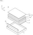
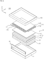
- FIG. 1 is an exploded perspective view showing a planar light source device according to an exemplary embodiment, not part of the invention.
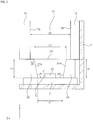
- FIG. 2 is a cross-sectional view showing the planar light source device according to the exemplary embodiment.
- the planar light source device 10 of the embodiment includes a light source module 20 for providing light and a light guide plate 13, the light guide plate 13 having a light introduction surface 131 for receiving light from the light source module 20 and a light emission surface 132, which has a larger area than the light introduction surface 13 and emits the light.
- the Z-axis illustrated in the drawings may be referred to as "the front”.
- the X-axis illustrated in the drawings may be referred to as “the horizontal direction” or “the longitudinal direction”.
- the Y-axis illustrated in the drawings may be referred to as "the upward direction”.
- the light guide plate 13 serves to diffuse and propagate the light introduced from the point light source of the light source module 20. That is, the light guide plate 13 may cause introduced point light to have even brightness, and may convert the introduced point light into planar light so that the planar light is emitted outward through the light emission surface 132.
- the light guide plate 13 may be made of a transparent material or a hollow metal pipe, into which light propagates.
- the light guide plate 13 may be fabricated and used in a flat type or a wedge type using polymethylmethacrylate (PMMA) or a transparent acryl resin, may be formed of a glass material, or may include a plastic lens, although the disclosure is not limited thereto.
- PMMA polymethylmethacrylate
- a transparent acryl resin may be formed of a glass material, or may include a plastic lens, although the disclosure is not limited thereto.
- the light guide plate 13 may take the form of a plate having 132 light emission surface 132, from which planar light is emitted, a light-reflecting surface 135 opposite the light emission surface 132, and four side surfaces connecting the light emission surface 132 and the light-reflecting surface 135 to each other.
- the form of the light guide plate 13 is not limited thereto.
- light may be emitted from the front and rear sides of the light guide plate 13 (both ends in the Z-axis direction).
- the light-reflecting surface 135 may be formed in such a manner as to provide a resin material with an aluminum layer imparted with excellent reflectivity through chemical vapor deposition, the aluminum layer being provided or not provided with a plurality of randomly arranged protrusions.
- the protrusions serve to reflect light, introduced from the point light sources 22, in various directions.
- the front surface of the light guide plate 13, i.e. the light emission surface 132, is forwardly spaced apart from the light-reflecting surface 135.
- the space between the light emission surface 132 and the light-reflecting surface 135 may be filled with air.
- the light emission surface 132 and the light-reflecting surface 135 are arranged parallel to each other in consideration of the efficient propagation of light.
- the light emission surface 132 may include a regular reflector pattern.
- the light emission surface 132 may downwardly reflect some of the light introduced through the light introduction surface 131 from the point light sources 22 so as to transmit the light in the direction opposite the light introduction surface 131.
- the remaining light, introduced through the light introduction surface 131 from the point light sources 22, may be forwardly emitted from the light guide plate 13 through the light emission surface 132.
- the light introduction surface 131 is a space which is located between the light-reflecting surface 135 and the light emission surface 132 so as to receive light from the point light sources 22 of the light source module 20.
- the light introduction surface 131 may be disposed on one side surface of the light guide plate 13, and may be made of a transparent material so as to be open.
- the area of the light introduction surface 131 is smaller than the area of the light emission surface 132.
- the light guide plate 13 may be formed of a light transmissive material, and may be configured so as to inwardly propagate the light introduced through the light introduction surface 131 of the light guide plate 13 using the difference in the index of refraction between the light guide plate and the outside.
- planar light source device 10 may further include at least one optical sheet 14, disposed in front of the light guide plate 13 so as to concentrate and diffuse the light directed from the light guide plate 13, and at least one reflector sheet 12 at the rear of the light guide plate 13.
- planar light source device 10 may further include a bottom cover 11 disposed below the light guide plate 13, the bottom cover 11 being configured to receive the light guide plate 13 and the light source module 20 therein.
- the reflector sheet 12 may be disposed at the rear of the light guide plate 13, the disclosure is not limited thereto.
- the reflector sheet 12 may enhance light transmission efficiency by reflecting the light, generated from the light source module 20, forward from the light guide plate 13.
- the optical sheet 14 serves to concentrate and diffuse the planar light introduced from the light guide plate 13.
- the optical sheet 14 may include a diffuser film 14a which includes diffuser particles such as, for example, beads, to diffuse the light introduced from the light guide plate 13 toward a liquid crystal display panel (in the forward direction), a prism film 14b which has a prism pattern to concentrate light in front of the diffuser film 14a, and a protector film 14c which covers the entire surface of the prism film 14b to protect the prism film 14b.
- a diffuser film 14a which includes diffuser particles such as, for example, beads, to diffuse the light introduced from the light guide plate 13 toward a liquid crystal display panel (in the forward direction)
- a prism film 14b which has a prism pattern to concentrate light in front of the diffuser film 14a
- a protector film 14c which covers the entire surface of the prism film 14b to protect the prism film 14b.
- the disclosure is not limited thereto.
- the optical sheet 14 may diffuse and concentrate the light, emitted from the light source module 20 and guided by the light guide plate 13, so as to achieve the required brightness and viewing angle.
- the diffuser film 14a may realize even brightness by scattering and concentrating the light coming from the light source module 20 or the light returning from the prism film 14b.
- the diffuser film 14a may have a thin sheet shape and may be formed of a transparent resin.
- the diffuser film 14a may be formed by coating a polycarbonate or polyester film with a light-scattering or light-concentrating resin.
- the disclosure is not limited thereto.
- the prism film 14b is acquired by forming a vertical or horizontal prism pattern on the surface of an optical film, and serves to concentrate light output from the diffuser film 14a.
- the prism pattern of the prism film 14b may be formed to have a triangular cross section in order to improve the light concentration efficiency thereof.
- the optimum brightness may be accomplished when a right-angled prism having an apex angle of 90 degrees is used.
- the protector film 14c may cover the upper surface of the prism film 14b in order to protect the prism film 14b.
- the light generated from the light source module 20 may be efficiently introduced into the light guide plate 13 only when a constant distance is maintained between the light guide plate 13 and the light source module 20.
- the light source module 20 is required to provide light that is uniform in the longitudinal direction of the light guide plate 13.
- FIG. 3 is a plan view showing the light source module according to the exemplary embodiment.
- the light source module 20 serves to generate light and provide the light to the light guide plate 13.
- the light source module 20 includes a plurality of point light sources 22 for generating light, the circuit board 21 on which the point light sources 22 are mounted, and a light guide for guiding the light generated from the point light sources 22.
- the point light sources 22 may include any of various components capable of generating light.
- the point light sources 22 are light sources capable of emitting point-shaped light.
- the point light sources 22 may include semiconductor diodes such as light-emitting diodes or laser diodes.
- the point light sources 22 may be of a chip-on-board type, in which light-emitting diodes are mounted on a circuit board 21.
- the disclosure is not limited thereto.
- the point light sources 22 may be colored light-emitting diodes which emit light having a color such as red, green, blue, white or the like, or ultra violet (UV) light-emitting diodes which emit ultraviolet light, the disclosure is not limited thereto.
- the light source module 20 may further include a fluorescent body (not shown) for converting the wavelength of light generated from the point light sources 22 into light having a white wavelength.
- the fluorescent body is disposed so as to surround the point light sources 22.
- the point light sources 22 may be arranged in a single row or in multiple rows.
- the point light sources 22 may be composed of light emitting elements adapted to emit red, green and blue colored light, which are alternately arranged.
- the point light sources 22 may be repeatedly arranged at a constant pitch in the longitudinal direction of the light introduction surface 131 of the light guide plate 13 (in the x-axis direction).
- the point light sources 22 are preferably arranged in a single row in the direction parallel to the longitudinal direction of the light introduction surface 131 of the light guide plate 13.
- Light generated from the point light sources 22 is emitted in a radial fashion around the light-projecting direction.
- the light-projecting direction of the point light sources 22 is typically perpendicular to the light introduction surface 131.
- the circuit board 21 serves to provide a space on which the point light sources 22 are disposed and to support the point light sources 22.
- the circuit board 21 may include an electrode pattern (not shown) having electrical conductivity, and an insulative body which surrounds the electrode pattern and has an opening portion (not shown) through which a portion of the electrode pattern is exposed.
- the point light sources 22 are electrically connected to the electrode pattern.
- the circuit board 21 is provided with a connector 26, which is electrically connected to an external power supply. The connector serves to electrically connect the circuit board 21 and the external power supply to each other.
- the body of the circuit board 21 may include a material having an electrical insulation property.
- the body of the circuit board 21 may be formed of FR-4, or may include at least one of polyimide, liquid crystal polymer, polyester, polyethylene naphthalate (PEN), polyethylene terephthalate (PET) and liquid crystal polymer (LCP), but the disclosure is not limited thereto.
- the circuit board 21 may be a typical printed circuit board (PCB), a metal core PCB, a flexible PCB, a ceramic PCB or the like.
- the circuit board 21 is disposed so as to face the light introduction surface 131 of the light guide plate 13. Specifically, the upper surface of the circuit board 21 is positioned so as to face the light introduction surface 131 of the light guide plate 13 in a state of being parallel to the light introduction surface 131.
- the circuit board 21 has a larger size than at least the light introduction surface 131 of the light guide plate 13. In other words, the circuit board 21 is positioned so as to overlap the light introduction surface 131 of the light guide plate 13.
- the circuit board 21 may be further provided on the upper surface thereof with a reflective layer (not shown), which serves to reflect light introduced into the upper surface of the circuit board 21.
- the reflective layer may be formed of a reflective material, which is applied to the entire upper surface of the circuit board 21.
- the reflective layer may include at least one of silver (Ag), aluminum (Al), a silver (Ag) alloy, and an aluminum (Al) alloy.
- the reflective surfaces may be configured such that layers having different indices of refraction are alternately and repeatedly stacked one on another.
- the reflective layer is not limited thereto.
- the point light sources 22 are arranged on the upper surface of the circuit board 21 in the longitudinal direction of the circuit board 21 (i.e. in the x-axis direction or in the longitudinal direction of the light introduction surface 131).
- the light guide serves to guide the light, emitted from the point light sources 22, in the upward direction of the circuit board 21. Furthermore, the light guide serves to guide the light, emitted from the point light sources 22, from the circuit board 21 to the light introduction surface 131 of the light guide plate 13.
- the light guide includes a first reflective wall 23 disposed on the upper surface of the circuit board 21, and a second reflective wall 24 disposed on the upper surface of the circuit board 21 so as to define a space C, in which the point light sources 22 are located, between the first reflective wall 23 and the second reflective wall 24.
- the first reflective wall 23, the second reflective wall 24, the upper surface of the circuit board 21, and the light introduction surface 131 of the light guide plate 13 define a closed space, and the point light sources 22 are located in the closed space.
- first reflective wall 23 and the second reflective wall 24 are arranged in the longitudinal direction of the circuit board 21.
- the first reflective wall 23 and the second reflective wall 24 have a length corresponding to the length of the light introduction surface 131 and are arranged parallel to each other.
- the first reflective wall 23 and the second reflective wall 24 support the light guide plate 13 to prevent the light guide plate 13 from coming into contact with the point light sources 22 and to maintain the distance between the point light sources 22 and the light guide plate 13.
- the first reflective wall 23 and the second reflective wall 24 reflect the light introduced from the point light sources 22.
- the reflective walls may be formed of a resin material.
- the first reflective wall 23 and the second reflective wall 24 cause the point light sources 22 and the light guide plate 13 to be spaced apart from each other, in order to prevent the light guide plate 13 from being deformed by the heat generated from the point light sources 22.
- at least one of the heights h1 and h2 of the first reflective wall 23 and the second reflective wall 24 is greater than the height of the point light sources 22.
- both the heights h1 and h2 of the first reflective wall 23 and the second reflective wall 24 may be greater than the height of the point light sources 22.
- the light introduction surface 131 of the light guide plate 13 is supported by at least one of the upper portion of the first reflective wall 23 and the upper portion of the second reflective wall 24. Specifically, the front end of the light introduction surface 131 of the light guide plate 13 is supported by the upper portion of the first reflective wall 23, and the rear end of the light introduction surface 131 is supported by the upper portion of the second reflective wall 24.
- the width d3 of the portion of the light introduction surface 131 of the light guide plate 13 that is supported by the first reflective wall 23 or the second reflective wall 24 preferably exceeds 0.01 mm.
- the first reflective wall 23 and the second reflective wall 24 are provided with reflective surfaces to reflect the light generated from the point light sources 22.
- the reflective surfaces may include at least one of silver (Ag), aluminum (Al), a silver (Ag) alloy, and an aluminum (Al) alloy.
- the reflective surfaces may be configured such that layers having different indices of refraction are alternately and repeatedly stacked one on another.
- the reflective surfaces include a first reflective surface 23a formed on one surface of the first reflective wall 23 to reflect light, and a second reflective surface 24a formed on one surface of the second reflective wall 24 to reflect light.
- the first reflective surface 23a and the second reflective surface 24a are arranged so as to face each other with the point light sources 22 interposed therebetween.
- the first reflective surface 23a and the second reflective surface 24a are configured so as to be parallel to each other.
- the space defined by the first reflective surface 23a and the second reflective surface 24a vertically overlaps the light introduction surface 131 of the light guide plate 13.
- the reflective surfaces serve to increase the amount of light that undergoes total reflection at the boundary of the light guide plate 13 when the light from the point light sources 22 is introduced through the light introduction surface 131 of the light guide plate 13. Accordingly, the light guide has to cause the light to be introduced into the light introduction surface 131 in a direction parallel to the light emission surface 132 of the light guide plate 13, or to ensure that the angle between the light emission surface 132 and the light introduced into the light introduction surface 131 is small.
- the distance between the first reflective surface 23a and the second reflective surface 24a may increase in at least some region with increasing distance from the bottom.
- Providing the reflective surfaces with the above-described shape may cause the light, generated from the point light sources 22, to be introduced into the light emission surface 131 of the light guide plate 13 in a direction approximately parallel to the light emission surface 132 of the light guide plate 13, which may reduce the loss of light inside the light guide plate 13.
- first reflective surface 23a and the second reflective surface 24a may be configured such that the distance therebetween increases with increasing distance upward from the bottom.
- first reflective surface 23a and the second reflective surface 24a may be configured such that the distance therebetween increases in the direction from the circuit board 21 toward the light guide plate 13.
- the width d2 between the upper end of the first reflective surface 23a and the upper end of the second reflective surface 24a may be smaller than the width d4 of the light introduction surface 131 of the light guide plate 13.
- the width d2 between the upper end of the first reflective surface 23a and the upper end of the second reflective surface 24a may be within a range from 90% to 95% of the width d4 of the light introduction surface 131 of the light guide plate 13. If the width d2 between the upper end of the first reflective surface 23a and the upper end of the second reflective surface 24a is less than 90% of the width d4 of the light introduction surface 131 of the light guide plate 13, hot spots may be generated on the light emission surface 132 at positions close to the light introduction surface 131.
- the reflective walls 23 and 24 may have difficulty supporting the light introduction surface 131 of the light guide plate 13.
- the width d2 between the upper end of the first reflective surface 23a and the upper end of the second reflective surface 24a is greater than the width d1 between the lower end of the first reflective surface 23a and the lower end of the second reflective surface 24a.
- the reflective surfaces may be flat or curved.
- the shapes of the first reflective surface 23a and the second reflective surface 24a may be configured to be symmetrical with each other, or may be different.
- the first reflective surface 23a and the second reflective surface 24a may be oriented at an angle that is perpendicular or oblique relative to the upper surface of the circuit board 21.
- the first reflective surface 23a and the second reflective surface 24a may have the same angle or different angles relative to the upper surface of the circuit board 21.
- FIG. 2 illustrates an example in which each of the first reflective surface 23a and the second reflective surface 24a has a flat surface, and the first reflective surface 23a and the second reflective surface 24a have the same angle relative to the upper surface of the circuit board 21.
- Various configurations of the reflective surfaces other than the above-mentioned configuration will be described later.
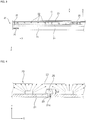
- FIG. 4 is a cross-sectional view of the light source module shown in FIG. 3 , which is taken along line A-A.
- the light source module 20 further includes bridges 25 configured to connect the first reflective wall 23 and the second reflective wall 24 to each other.
- the bridges 25 serve to prevent bending which may occur when the first reflective wall 23 and the second reflective wall 24 are long so as to maintain a constant distance between the first reflective wall 23 and the second reflective wall 24, thereby allowing the first reflective wall 23 and the second reflective wall 24 to be integrally coupled to the circuit board 21.
- Each of the bridges 25 has one end connected to the first reflective wall 23 and the other end connected to the second reflective wall 24.
- the bridges 25 may be repeatedly arranged at a constant pitch in the longitudinal direction of the circuit board 21.
- the bridges 25 are located between the point light sources 22, which are arranged in the longitudinal direction of the circuit board 21.
- the height h3 of the bridges 25 is not limited, in order to allow the light generated from the point light sources 22 to be emitted in the longitudinal direction of the light introduction surface 131 without restriction, the height h3 of the bridges 25 is preferably lower than those of the first reflective wall 23 and the second reflective wall 24.
- a reflective material for reflecting light may be applied to the outer surfaces of the bridges 25.
- the reflective material is the same material as that of the above-described reflector layer.
- each bridge 25 is preferably configured such that the width of the bridge is gradually reduced with increasing distance upward from the bottom (i.e. in the direction from the circuit board 21 toward the light guide plate 13).
- the bridges 25 are disposed on the upper surface of the circuit board 21.
- the light guide may further include coupling protrusions 29, which are fitted into respective coupling holes 21a formed in the circuit board 21.
- the coupling protrusions 29 serve to position the coupling locations and to provide holding force when the light guide is coupled to the circuit board 21.
- the light guide may be coupled to the circuit board 21 by means of a bonding material.
- the coupling protrusions 29 include at least two coupling protrusions in order to prevent rotation and displacement of the light guide. Specifically, the coupling protrusions 29 protrude from the bottom of the light guide. More specifically, the coupling protrusions 29 may protrude from the bottom of the bridges 25.
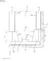
- FIG. 5 is a schematic view illustrating a light travelling path of the planar light source device according to the exemplary embodiment.
- FIG. 5A is a cross-sectional view of the planar light source device, which is take along the Y-Z cross section.
- the distance between the first reflective surface 23a and the second reflective surface 24a increases in at least a portion thereof with increasing distance upward from the bottom, and light generated from the point light sources 22 is thus introduced into the light introduction surface 131 of the light guide plate 13 at an angle approximately parallel to the light emission surface 132 of the light guide plate 13. Accordingly, when the light generated from the point light sources 22 is introduced into the light introduction surface 131 of the light guide plate 13 at an angle approximately parallel to the light emission surface 132 of the light guide plate 13, it is possible to reduce the loss of light in the light guide plate 13.
- FIG. 5B is a cross-sectional view of the planar light source device, which is taken along the X-Y cross section.
- the space defined by the first reflective surface 23a and the second reflective surface 24a extends in the longitudinal direction of the light introduction surface 131, and the point light sources 22 are arranged on the upper surface of the circuit board 21 in a chip-on-board fashion, thereby allowing light generated from the point light sources 22 to be efficiently emitted in the longitudinal direction of the light introduction surface 131. Consequently, light generated from the plurality of point light sources 22 is emitted in the longitudinal direction of the light introduction surface 131 in a fashion similar to a planar light source. Accordingly, the light may be uniformly introduced into the light introduction surface 131 of the light guide plate 13 from the plurality of point light sources 22.
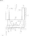
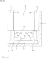
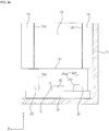
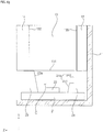
- FIGS. 6A to 6G are views showing light guides according to various embodiments.
- the light guides shown in FIGS. 6A to 6G are modifications of the light guide shown in FIG. 2 , and a description of configurations that are identical to those shown in FIG. 2 is omitted.
- the light guide according to the invention is configured such that height of the first reflective wall 23 is different from that of the second reflective wall 24.
- any of the height of the first reflective 23 and the height of the second reflective wall 24 is also greater than the height of the point light sources 22.
- the light introduction surface 131 of the light guide plate 13 includes a stepped portion 131a, which is recessed or protruded therefrom.
- the stepped portion 131a mates with the upper portion of the first reflective wall 23 or the second reflective wall 24 so as to position the light guide plate 13 with respect to the light source module 20.
- the height h2 of the second reflective wall 24 is greater than the height h1 of the first reflective wall 23.
- FIG. 6B a further embodiment, not part of the invention, differs from the embodiment shown in FIG. 2 in terms of the shapes of the first reflective surface 23a and the second reflective surface 24a.
- the first reflective surface 23a and the second reflective surface 24a are curved. Specifically, the first reflective surface 23a and the second reflective surface 24a define aspherical or spherical surfaces, which have the centers of curvature positioned directly above the point light sources 22.
- a further embodiment differs from the embodiment shown in FIG. 2 in terms of the shape of the first reflective surface 23a.
- the first reflective surface 23a and the second reflective surface 24a have angle of inclination that are different from each other.
- the angle of inclination ⁇ 1 defined between the first reflective surface 23a and the upper surface of the circuit board 21, is a right angle
- the angle of inclination ⁇ 2, defined between the second reflective surface 24a and the upper surface of the circuit board 21 is greater than a right angle.
- a further embodiment differs from the embodiment shown in FIG. 2 in terms of shapes of the first reflective surface 23a and the second reflective surface 24a.
- the first reflective surface 23a and the second reflective surface 24a have shapes that are symmetrical to each other.
- the distance between the lower section 231 of the first reflective surface 23a and a lower section 241 of the second reflective surface 24a increases with increasing distance toward the light guide plate 13 from the circuit board 21, and the distance between the upper section 232 of the first reflective surfaces 23a and the upper section 242 of the second reflective surface 24a is constant.
- a height of the lower sections 231 and 241 of the first and second reflective surfaces 23a and 24a may be equal to or greater than the height of the point light sources 22.
- a further embodiment, not part of the invention, differs from the embodiment shown in FIG. 6D in terms of the shape of the first reflective surface 23a.
- the first and second reflective surfaces 23a and 24a have shapes that are different from each other.
- the second reflective surface 24a of this embodiment is identical to the second reflective surface 24a of the embodiment shown in FIG. 6D
- the first reflective surface 23a of this embodiment has an angle of inclination perpendicular to the upper surface of the circuit board 21, unlike the embodiment shown in FIG. 6D .
- a further embodiment differs from the embodiment shown in FIG. 2 in terms of the shape of the second reflective surface 24a.
- one of two reflective surfaces has a flat surface and the other of the two reflective surfaces has a curved surface.
- the distance between the first reflective surface 23a and the second reflective surface 24a increases with increasing distance from the circuit board 21 toward the light guide plate 13.
- the first reflective surface 23a is flat whereas the second reflective surface 24a is curved.
- a further embodiment, not part of the invention, differs from the embodiment shown in FIG. 6D in terms of the shape of the first reflective surface 23a.
- the first and second reflective surfaces 23a and 24a have shapes that are different from each other.
- the second reflective surface 24a of this embodiment is identical to the second reflective surface 24a of the embodiment shown in FIG. 6D
- the first reflective surface 23a of this embodiment has an angle of inclination that is greater than a right angle unlike the embodiment shown in FIG. 6D .
- the height of the lower section 241 of the second reflective surface 24a may be equal to or greater than the height of the point light sources 22.
- FIG. 7 is a cross-sectional view showing a planar light source device according to a further embodiment, not part of the invention.
- the planar light source device of this embodiment differs from that of the embodiment shown in FIG. 2 in terms of the configuration of the light source module 20.
- one of two reflective walls has a greater width than the other of the two reflective walls. Increasing the width of one of two reflective walls may contribute to an increase in the rigidity of the light guide and prevent distortion of the light guide.
- the point light sources 22 may eccentrically deviate to one side in the width direction of the circuit board 21 (in the z-axis direction).
- the first reflective wall 23 has a greater width d5 than the second reflective wall 24.
- the widths of the upper and lower ends of the first reflective wall 23 are greater than those of the upper and lower ends of the second reflective wall 24.
- the light guide plate 13 and the optical sheet 14 may be disposed on the upper end of the first reflective wall 23, which has an increased width and may be stably supported thereby.
- the reflective walls maintain a uniform distance between the light guide plate and the point light sources, there is an advantage of preventing the light guide plate from being deformed by heat generated from the point light sources.
- FIG. 8 is an exploded perspective view showing a liquid crystal display apparatus including the planar light source device.
- the liquid crystal display apparatus 100 of the embodiment may include a liquid crystal display panel 110, which displays an image, and the planar light source device 10, which supplies light to the liquid crystal display panel 110.
- the liquid crystal display panel 110 may display an image using the light provided from the planar light source device 10.
- the liquid crystal display panel 110 may include a color filter substrate 112 and a thin film transistor substrate 114 which are opposite each other with liquid crystals interposed therebetween.
- the color filter substrate 112 may realize the color of the image displayed on the liquid crystal display panel 110.
- the thin film transistor substrate 114 is electrically connected to a printed circuit board 118, on which a plurality of circuit components are mounted, via a drive film 117.
- the thin film transistor substrate 114 may apply a drive voltage, provided from the printed circuit board 118, to the liquid crystals in response to a drive signal provided from the printed circuit board 118.
- the thin film transistor substrate 114 may include thin film transistors and pixel electrodes formed on a transparent substrate formed of, for example, glass or plastic.
- the liquid crystal display apparatus 100 may achieve good light uniformity and may prevent the generation of hot spots at the edge portion thereof.
Landscapes
- Physics & Mathematics (AREA)
- Optics & Photonics (AREA)
- General Physics & Mathematics (AREA)
- Engineering & Computer Science (AREA)
- General Engineering & Computer Science (AREA)
- Nonlinear Science (AREA)
- Microelectronics & Electronic Packaging (AREA)
- Mathematical Physics (AREA)
- Chemical & Material Sciences (AREA)
- Crystallography & Structural Chemistry (AREA)
- Planar Illumination Modules (AREA)
Description
- Embodiments relate to a light source module and a planar light source device.
- A representative example of light-emitting elements is Light-Emitting Diodes (LEDs), which convert electrical signals into infrared light, visible light, and the like using the characteristics of compound semiconductors. LEDs are used in, for example, home appliances, remote controllers, electronic display boards, display devices, and various automated devices. The fields in which LEDs are used are gradually becoming more numerous.
- A planar light source device equipped with LEDs is a device that converts light, which is emitted from LEDs in a point light source form, into a planar light form. The planar light source device may be used in a display apparatus such as a liquid crystal display apparatus, and may be used in a variety of other lighting apparatuses.
- In a conventional light guide structure, light is introduced from a light source, located at one side when viewing a cross-section of a light guide unit, into the light guide unit so as to be guided to a light emission surface or a surface opposite the light source. A light guiding means is a total reflection or light emission means based on the difference in the index of refraction, and such a means uses a pattern or shape to cause light to be emitted from the light emission surface.
-
FIG. 9 is a cross-sectional view of a conventional planar light source device, taken along the longitudinal direction of a light source module. Referring toFIG. 9 , the conventional light source module is constructed such thatpackages 1300 are disposed so as to surroundpoint light sources 1200. The packagedpoint light sources 1200 are arranged at a constant pitch in the longitudinal direction of acircuit board 1100. - In order to concentrate light generated from the
point light sources 1200 in a desired direction, thepackages 1300 are configured so as to be open at upper sides thereof over thepoint light sources 120 and to surround the side surfaces of the point light sources 1200.1 - Although the
packages 1300 may concentrate light, generated from thepoint light sources 1200, upward (toward a light guide plate 1400), there is a problem in that the amount of light emitted in a lateral direction is reduced, thereby causing the occurrence of hot spots between thepoint light sources 120. - For this reason, if the pitch between the
point light sources 1200 is decreased in order to diminish the hot spots, there is a problem in that manufacturing costs are increased. -
FIG. 10 illustrates the travelling path of light introduced from a light source module in which the light is guided toward alight guide plate 1400 by means of alight guide 1500. - Here, the
light guide 1500 is configured such that the width thereof is reduced with increasing distance toward thelight guide plate 1400 from thepoint light sources 1200. - Consequently, there is a problem in that the light introduced from the
point light sources 1200 undergoes total reflection in thelight guide 1500, thereby causing internal loss of light. Furthermore, when light emitted from thelight guide 1500 is introduced into thelight guide plate 1400, some of the light introduced at an angle exceeding an acceptance angle (the maximum allowable incident angle within which the light emitted from thelight guide plate 1400 can undergo total reflection), thereby causing radiation loss in thelight guide plate 1400. - The formula for calculating the acceptance angle is as follows:

US 2015/062494 discloses a light emitting module that includes at least one light emitting chip mounted on a substrate, a sidewall including a fastener fastened to the substrate and surrounding the light emitting chip, and a transparent resin mixed with phosphor configured to fill a space partitioned by the sidewall. - The present invention provides a light source module and a planar light source device according to
claim 1. - Details of the embodiments will be more clearly understood from the following detailed
description taken in conjunction with the accompanying drawings, in which: -
FIG. 1 is an exploded perspective view showing a planar light source device according to an exemplary embodiment, not part of the invention; -
FIG. 2 is a cross-sectional view showing the planar light source device according to the exemplary embodiment; -
FIG. 3 is a plan view showing a light source module according to the exemplary embodiment; -
FIG. 4 is a cross-sectional view of the light source module shown inFIG. 3 , which is taken along line A-A; -
FIG. 5 is a schematic view illustrating a light travelling path of the planar light source device according to the exemplary embodiment; -
FIGS. 6A shows a light guide according to the invention; -
FIGS 6B-6G are views showing light guides according to various embodiments, not part of the invention; -
FIG. 7 is a cross-sectional view illustrating the planar light source device according to another embodiment, not part of the invention; -
FIG. 8 is an exploded perspective view showing a liquid crystal display apparatus including the planar light source device; -
FIG. 9 is a cross-sectional view showing a planar light source device according to the related art; and -
FIG. 10 is a view illustrating a light guide according to the related art which decreases in width with increasing distance toward a light guide plate. - Reference will now be made in detail to embodiments, examples of which are illustrated in the accompanying drawings. However, the present disclosure may be embodied in many different forms and should not be construed as limited to the embodiments set forth herein. Rather, these embodiments are provided so that this disclosure will be thorough and complete, and will fully convey the scope of the disclosure to those skilled in the art. The present disclosure is defined only by the categories of the claims. In certain embodiments, detailed descriptions of device constructions or processes well known in the art may be omitted to avoid obscuring appreciation of the disclosure by a person of ordinary skill in the art. Wherever possible, the same reference numbers will be used throughout the drawings to refer to the same or like parts.
- Spatially relative terms such as "below", "beneath", "lower", "above", or "upper" may be used herein to describe one element's relationship to another element as illustrated in the Figures. It will be understood that spatially relative terms are intended to encompass different orientations of the device in addition to the orientation depicted in the Figures. For example, if the device in one of the figures is turned over, elements described as "below" or "beneath" other elements would then be oriented "above" the other elements. The exemplary terms "below" or "beneath" can, therefore, encompass both an orientation of above and below. Since the device may be oriented in another direction, the spatially relative terms may be interpreted in accordance with the orientation of the device.
- The terminology used in the present disclosure is for the purpose of describing particular embodiments only and is not intended to limit the disclosure. As used in the disclosure and the appended claims, the singular forms "a", "an" and "the" are intended to include the plural forms as well, unless the context clearly indicates otherwise. It will be further understood that the terms "comprises" and/or "comprising," when used in this specification, specify the presence of stated features, integers, steps, operations, elements, and/or components, but do not preclude the presence or addition of one or more other features, integers, steps, operations, elements, components, and/or groups thereof.
- Unless otherwise defined, all terms (including technical and scientific terms) used herein have the same meaning as commonly understood by one of ordinary skill in the art. It will be further understood that terms, such as those defined in commonly used dictionaries, should be interpreted as having a meaning that is consistent with their meaning in the context of the relevant art and the present disclosure, and will not be interpreted in an idealized or overly formal sense unless expressly so defined herein.
- In the drawings, the thickness or size of each layer is exaggerated, omitted, or schematically illustrated for convenience of description and clarity. Also, the size or area of each constituent element does not entirely reflect the actual size thereof.
- Angles or directions used to describe the structures of light-emitting devices according to embodiments are based on those shown in the drawings. Unless there is, in the specification, no definition of a reference point to describe angular positional relationships in the structures of the light-emitting devices, the associated drawings may be referred to.
-
FIG. 1 is an exploded perspective view showing a planar light source device according to an exemplary embodiment, not part of the invention.FIG. 2 is a cross-sectional view showing the planar light source device according to the exemplary embodiment. - Referring to
FIGs. 1 and2 , the planarlight source device 10 of the embodiment includes alight source module 20 for providing light and alight guide plate 13, thelight guide plate 13 having alight introduction surface 131 for receiving light from thelight source module 20 and alight emission surface 132, which has a larger area than thelight introduction surface 13 and emits the light. - First, the Z-axis illustrated in the drawings may be referred to as "the front". The X-axis illustrated in the drawings may be referred to as "the horizontal direction" or "the longitudinal direction". The Y-axis illustrated in the drawings may be referred to as "the upward direction".
- The
light guide plate 13 serves to diffuse and propagate the light introduced from the point light source of thelight source module 20. That is, thelight guide plate 13 may cause introduced point light to have even brightness, and may convert the introduced point light into planar light so that the planar light is emitted outward through thelight emission surface 132. - For example, the
light guide plate 13 may be made of a transparent material or a hollow metal pipe, into which light propagates. Specifically, thelight guide plate 13 may be fabricated and used in a flat type or a wedge type using polymethylmethacrylate (PMMA) or a transparent acryl resin, may be formed of a glass material, or may include a plastic lens, although the disclosure is not limited thereto. - In particular, referring to
FIG. 2 , thelight guide plate 13 may take the form of a plate having 132light emission surface 132, from which planar light is emitted, a light-reflectingsurface 135 opposite thelight emission surface 132, and four side surfaces connecting thelight emission surface 132 and the light-reflectingsurface 135 to each other. However, the form of thelight guide plate 13 is not limited thereto. In addition, in another embodiment, light may be emitted from the front and rear sides of the light guide plate 13 (both ends in the Z-axis direction). - The light-reflecting
surface 135 of thelight guide plate 13, which constitutes the rear surface of thelight guide plate 13, performs total forward (Z-axis) reflection of the light introduced from the pointlight sources 22 through thelight introduction surface 131. - For example, the light-reflecting
surface 135 may be formed in such a manner as to provide a resin material with an aluminum layer imparted with excellent reflectivity through chemical vapor deposition, the aluminum layer being provided or not provided with a plurality of randomly arranged protrusions. The protrusions serve to reflect light, introduced from the pointlight sources 22, in various directions. - The front surface of the
light guide plate 13, i.e. thelight emission surface 132, is forwardly spaced apart from the light-reflectingsurface 135. The space between thelight emission surface 132 and the light-reflectingsurface 135 may be filled with air. Thelight emission surface 132 and the light-reflectingsurface 135 are arranged parallel to each other in consideration of the efficient propagation of light. - Specifically, the
light emission surface 132 may include a regular reflector pattern. Thelight emission surface 132 may downwardly reflect some of the light introduced through thelight introduction surface 131 from the pointlight sources 22 so as to transmit the light in the direction opposite thelight introduction surface 131. The remaining light, introduced through thelight introduction surface 131 from the pointlight sources 22, may be forwardly emitted from thelight guide plate 13 through thelight emission surface 132. - The
light introduction surface 131 is a space which is located between the light-reflectingsurface 135 and thelight emission surface 132 so as to receive light from the pointlight sources 22 of thelight source module 20. - For example, as shown in
FIG. 2 , thelight introduction surface 131 may be disposed on one side surface of thelight guide plate 13, and may be made of a transparent material so as to be open. In particular, the area of thelight introduction surface 131 is smaller than the area of thelight emission surface 132. - In another example, the
light guide plate 13 may be formed of a light transmissive material, and may be configured so as to inwardly propagate the light introduced through thelight introduction surface 131 of thelight guide plate 13 using the difference in the index of refraction between the light guide plate and the outside. - In addition, the planar
light source device 10 may further include at least oneoptical sheet 14, disposed in front of thelight guide plate 13 so as to concentrate and diffuse the light directed from thelight guide plate 13, and at least onereflector sheet 12 at the rear of thelight guide plate 13. - In addition, the planar
light source device 10 may further include abottom cover 11 disposed below thelight guide plate 13, thebottom cover 11 being configured to receive thelight guide plate 13 and thelight source module 20 therein. - Although the
reflector sheet 12 may be disposed at the rear of thelight guide plate 13, the disclosure is not limited thereto. Thereflector sheet 12 may enhance light transmission efficiency by reflecting the light, generated from thelight source module 20, forward from thelight guide plate 13. - The
optical sheet 14 serves to concentrate and diffuse the planar light introduced from thelight guide plate 13. For example, theoptical sheet 14 may include adiffuser film 14a which includes diffuser particles such as, for example, beads, to diffuse the light introduced from thelight guide plate 13 toward a liquid crystal display panel (in the forward direction), aprism film 14b which has a prism pattern to concentrate light in front of thediffuser film 14a, and aprotector film 14c which covers the entire surface of theprism film 14b to protect theprism film 14b. However, the disclosure is not limited thereto. - The
optical sheet 14 may diffuse and concentrate the light, emitted from thelight source module 20 and guided by thelight guide plate 13, so as to achieve the required brightness and viewing angle. - The
diffuser film 14a may realize even brightness by scattering and concentrating the light coming from thelight source module 20 or the light returning from theprism film 14b. Thediffuser film 14a may have a thin sheet shape and may be formed of a transparent resin. For example, thediffuser film 14a may be formed by coating a polycarbonate or polyester film with a light-scattering or light-concentrating resin. However, the disclosure is not limited thereto. - The
prism film 14b is acquired by forming a vertical or horizontal prism pattern on the surface of an optical film, and serves to concentrate light output from thediffuser film 14a. - The prism pattern of the
prism film 14b may be formed to have a triangular cross section in order to improve the light concentration efficiency thereof. The optimum brightness may be accomplished when a right-angled prism having an apex angle of 90 degrees is used. - The
protector film 14c may cover the upper surface of theprism film 14b in order to protect theprism film 14b. - The light generated from the
light source module 20 may be efficiently introduced into thelight guide plate 13 only when a constant distance is maintained between thelight guide plate 13 and thelight source module 20. In particular, in response to the recent trend toward planar light sources having reduced thickness, thelight source module 20 is required to provide light that is uniform in the longitudinal direction of thelight guide plate 13. -
FIG. 3 is a plan view showing the light source module according to the exemplary embodiment. - Referring to
FIGS. 1 to 3 , thelight source module 20 serves to generate light and provide the light to thelight guide plate 13. - For example, the
light source module 20 includes a plurality of pointlight sources 22 for generating light, thecircuit board 21 on which the pointlight sources 22 are mounted, and a light guide for guiding the light generated from the pointlight sources 22. - The point
light sources 22 may include any of various components capable of generating light. For example, the pointlight sources 22 are light sources capable of emitting point-shaped light. The pointlight sources 22 may include semiconductor diodes such as light-emitting diodes or laser diodes. - Specifically, as shown in
FIG. 3 , the pointlight sources 22 may be of a chip-on-board type, in which light-emitting diodes are mounted on acircuit board 21. However, the disclosure is not limited thereto. - Although the point
light sources 22 may be colored light-emitting diodes which emit light having a color such as red, green, blue, white or the like, or ultra violet (UV) light-emitting diodes which emit ultraviolet light, the disclosure is not limited thereto. Thelight source module 20 may further include a fluorescent body (not shown) for converting the wavelength of light generated from the pointlight sources 22 into light having a white wavelength. The fluorescent body is disposed so as to surround the pointlight sources 22. - In addition, the point
light sources 22 may be arranged in a single row or in multiple rows. Specifically, the pointlight sources 22 may be composed of light emitting elements adapted to emit red, green and blue colored light, which are alternately arranged. - More specifically, the point
light sources 22 may be repeatedly arranged at a constant pitch in the longitudinal direction of thelight introduction surface 131 of the light guide plate 13 (in the x-axis direction). The pointlight sources 22 are preferably arranged in a single row in the direction parallel to the longitudinal direction of thelight introduction surface 131 of thelight guide plate 13. - Light generated from the point
light sources 22 is emitted in a radial fashion around the light-projecting direction. The light-projecting direction of the pointlight sources 22 is typically perpendicular to thelight introduction surface 131. - The
circuit board 21 serves to provide a space on which the pointlight sources 22 are disposed and to support the pointlight sources 22. For example, thecircuit board 21 may include an electrode pattern (not shown) having electrical conductivity, and an insulative body which surrounds the electrode pattern and has an opening portion (not shown) through which a portion of the electrode pattern is exposed. The pointlight sources 22 are electrically connected to the electrode pattern. Thecircuit board 21 is provided with aconnector 26, which is electrically connected to an external power supply. The connector serves to electrically connect thecircuit board 21 and the external power supply to each other. - The body of the
circuit board 21 may include a material having an electrical insulation property. For example, the body of thecircuit board 21 may be formed of FR-4, or may include at least one of polyimide, liquid crystal polymer, polyester, polyethylene naphthalate (PEN), polyethylene terephthalate (PET) and liquid crystal polymer (LCP), but the disclosure is not limited thereto. Thecircuit board 21 may be a typical printed circuit board (PCB), a metal core PCB, a flexible PCB, a ceramic PCB or the like. - The
circuit board 21 is disposed so as to face thelight introduction surface 131 of thelight guide plate 13. Specifically, the upper surface of thecircuit board 21 is positioned so as to face thelight introduction surface 131 of thelight guide plate 13 in a state of being parallel to thelight introduction surface 131. Thecircuit board 21 has a larger size than at least thelight introduction surface 131 of thelight guide plate 13. In other words, thecircuit board 21 is positioned so as to overlap thelight introduction surface 131 of thelight guide plate 13. - The
circuit board 21 may be further provided on the upper surface thereof with a reflective layer (not shown), which serves to reflect light introduced into the upper surface of thecircuit board 21. For example, the reflective layer may be formed of a reflective material, which is applied to the entire upper surface of thecircuit board 21. - For example, the reflective layer may include at least one of silver (Ag), aluminum (Al), a silver (Ag) alloy, and an aluminum (Al) alloy. In another example, the reflective surfaces may be configured such that layers having different indices of refraction are alternately and repeatedly stacked one on another. However, the reflective layer is not limited thereto.
- Here, the point
light sources 22 are arranged on the upper surface of thecircuit board 21 in the longitudinal direction of the circuit board 21 (i.e. in the x-axis direction or in the longitudinal direction of the light introduction surface 131). - The light guide serves to guide the light, emitted from the point
light sources 22, in the upward direction of thecircuit board 21. Furthermore, the light guide serves to guide the light, emitted from the pointlight sources 22, from thecircuit board 21 to thelight introduction surface 131 of thelight guide plate 13. - The light guide includes a first
reflective wall 23 disposed on the upper surface of thecircuit board 21, and a secondreflective wall 24 disposed on the upper surface of thecircuit board 21 so as to define a space C, in which the pointlight sources 22 are located, between the firstreflective wall 23 and the secondreflective wall 24. - Specifically, when the Y-Z cross-section is viewed, the first
reflective wall 23, the secondreflective wall 24, the upper surface of thecircuit board 21, and thelight introduction surface 131 of thelight guide plate 13 define a closed space, and the pointlight sources 22 are located in the closed space. - More specifically, the first
reflective wall 23 and the secondreflective wall 24 are arranged in the longitudinal direction of thecircuit board 21. The firstreflective wall 23 and the secondreflective wall 24 have a length corresponding to the length of thelight introduction surface 131 and are arranged parallel to each other. - The first
reflective wall 23 and the secondreflective wall 24 support thelight guide plate 13 to prevent thelight guide plate 13 from coming into contact with the pointlight sources 22 and to maintain the distance between the pointlight sources 22 and thelight guide plate 13. In addition, the firstreflective wall 23 and the secondreflective wall 24 reflect the light introduced from the pointlight sources 22. The reflective walls may be formed of a resin material. - The first
reflective wall 23 and the secondreflective wall 24 cause the pointlight sources 22 and thelight guide plate 13 to be spaced apart from each other, in order to prevent thelight guide plate 13 from being deformed by the heat generated from the pointlight sources 22. Thus, at least one of the heights h1 and h2 of the firstreflective wall 23 and the secondreflective wall 24 is greater than the height of the pointlight sources 22. In other words, both the heights h1 and h2 of the firstreflective wall 23 and the secondreflective wall 24 may be greater than the height of the pointlight sources 22. - The
light introduction surface 131 of thelight guide plate 13 is supported by at least one of the upper portion of the firstreflective wall 23 and the upper portion of the secondreflective wall 24. Specifically, the front end of thelight introduction surface 131 of thelight guide plate 13 is supported by the upper portion of the firstreflective wall 23, and the rear end of thelight introduction surface 131 is supported by the upper portion of the secondreflective wall 24. The width d3 of the portion of thelight introduction surface 131 of thelight guide plate 13 that is supported by the firstreflective wall 23 or the secondreflective wall 24 preferably exceeds 0.01 mm. - The first
reflective wall 23 and the secondreflective wall 24 are provided with reflective surfaces to reflect the light generated from the pointlight sources 22. The reflective surfaces may include at least one of silver (Ag), aluminum (Al), a silver (Ag) alloy, and an aluminum (Al) alloy. In another example, the reflective surfaces may be configured such that layers having different indices of refraction are alternately and repeatedly stacked one on another. - The reflective surfaces include a first
reflective surface 23a formed on one surface of the firstreflective wall 23 to reflect light, and a secondreflective surface 24a formed on one surface of the secondreflective wall 24 to reflect light. - The first
reflective surface 23a and the secondreflective surface 24a are arranged so as to face each other with the pointlight sources 22 interposed therebetween. The firstreflective surface 23a and the secondreflective surface 24a are configured so as to be parallel to each other. The space defined by the firstreflective surface 23a and the secondreflective surface 24a vertically overlaps thelight introduction surface 131 of thelight guide plate 13. - The reflective surfaces serve to increase the amount of light that undergoes total reflection at the boundary of the
light guide plate 13 when the light from the pointlight sources 22 is introduced through thelight introduction surface 131 of thelight guide plate 13. Accordingly, the light guide has to cause the light to be introduced into thelight introduction surface 131 in a direction parallel to thelight emission surface 132 of thelight guide plate 13, or to ensure that the angle between thelight emission surface 132 and the light introduced into thelight introduction surface 131 is small. - Therefore, particularly referring to FIG. 13, when the Y-Z cross section is viewed, the distance between the first
reflective surface 23a and the secondreflective surface 24a may increase in at least some region with increasing distance from the bottom. Providing the reflective surfaces with the above-described shape may cause the light, generated from the pointlight sources 22, to be introduced into thelight emission surface 131 of thelight guide plate 13 in a direction approximately parallel to thelight emission surface 132 of thelight guide plate 13, which may reduce the loss of light inside thelight guide plate 13. - Specifically, the first
reflective surface 23a and the secondreflective surface 24a may be configured such that the distance therebetween increases with increasing distance upward from the bottom. In other words, the firstreflective surface 23a and the secondreflective surface 24a may be configured such that the distance therebetween increases in the direction from thecircuit board 21 toward thelight guide plate 13. - The width d2 between the upper end of the first
reflective surface 23a and the upper end of the secondreflective surface 24a may be smaller than the width d4 of thelight introduction surface 131 of thelight guide plate 13. The width d2 between the upper end of the firstreflective surface 23a and the upper end of the secondreflective surface 24a may be within a range from 90% to 95% of the width d4 of thelight introduction surface 131 of thelight guide plate 13. If the width d2 between the upper end of the firstreflective surface 23a and the upper end of the secondreflective surface 24a is less than 90% of the width d4 of thelight introduction surface 131 of thelight guide plate 13, hot spots may be generated on thelight emission surface 132 at positions close to thelight introduction surface 131. If the width d2 between the upper end of the firstreflective surface 23a and the upper end of the secondreflective surface 24a exceeds 95% of the width d4 of thelight introduction surface 131 of thelight guide plate 13, thereflective walls light introduction surface 131 of thelight guide plate 13. - In addition, the width d2 between the upper end of the first
reflective surface 23a and the upper end of the secondreflective surface 24a is greater than the width d1 between the lower end of the firstreflective surface 23a and the lower end of the secondreflective surface 24a. - The reflective surfaces may be flat or curved. In addition, the shapes of the first
reflective surface 23a and the secondreflective surface 24a may be configured to be symmetrical with each other, or may be different. The firstreflective surface 23a and the secondreflective surface 24a may be oriented at an angle that is perpendicular or oblique relative to the upper surface of thecircuit board 21. Here, the firstreflective surface 23a and the secondreflective surface 24a may have the same angle or different angles relative to the upper surface of thecircuit board 21. -
FIG. 2 illustrates an example in which each of the firstreflective surface 23a and the secondreflective surface 24a has a flat surface, and the firstreflective surface 23a and the secondreflective surface 24a have the same angle relative to the upper surface of thecircuit board 21. Various configurations of the reflective surfaces other than the above-mentioned configuration will be described later. -
FIG. 4 is a cross-sectional view of the light source module shown inFIG. 3 , which is taken along line A-A. - Referring to
FIG. 4 , thelight source module 20 further includesbridges 25 configured to connect the firstreflective wall 23 and the secondreflective wall 24 to each other. - The
bridges 25 serve to prevent bending which may occur when the firstreflective wall 23 and the secondreflective wall 24 are long so as to maintain a constant distance between the firstreflective wall 23 and the secondreflective wall 24, thereby allowing the firstreflective wall 23 and the secondreflective wall 24 to be integrally coupled to thecircuit board 21. - Each of the
bridges 25 has one end connected to the firstreflective wall 23 and the other end connected to the secondreflective wall 24. Thebridges 25 may be repeatedly arranged at a constant pitch in the longitudinal direction of thecircuit board 21. Thebridges 25 are located between the pointlight sources 22, which are arranged in the longitudinal direction of thecircuit board 21. - Although the height h3 of the
bridges 25 is not limited, in order to allow the light generated from the pointlight sources 22 to be emitted in the longitudinal direction of thelight introduction surface 131 without restriction, the height h3 of thebridges 25 is preferably lower than those of the firstreflective wall 23 and the secondreflective wall 24. - In order to reflect the light introduced into the
bridges 25, a reflective material for reflecting light may be applied to the outer surfaces of thebridges 25. Here, the reflective material is the same material as that of the above-described reflector layer. - In addition, although the shape of the
bridges 25 is not limited, eachbridge 25 is preferably configured such that the width of the bridge is gradually reduced with increasing distance upward from the bottom (i.e. in the direction from thecircuit board 21 toward the light guide plate 13). Thebridges 25 are disposed on the upper surface of thecircuit board 21. - The light guide may further include
coupling protrusions 29, which are fitted intorespective coupling holes 21a formed in thecircuit board 21. The coupling protrusions 29 serve to position the coupling locations and to provide holding force when the light guide is coupled to thecircuit board 21. The light guide may be coupled to thecircuit board 21 by means of a bonding material. - The coupling protrusions 29 include at least two coupling protrusions in order to prevent rotation and displacement of the light guide. Specifically, the
coupling protrusions 29 protrude from the bottom of the light guide. More specifically, thecoupling protrusions 29 may protrude from the bottom of thebridges 25. -
FIG. 5 is a schematic view illustrating a light travelling path of the planar light source device according to the exemplary embodiment. -
FIG. 5A is a cross-sectional view of the planar light source device, which is take along the Y-Z cross section. Referring toFIG. 5A , the distance between the firstreflective surface 23a and the secondreflective surface 24a increases in at least a portion thereof with increasing distance upward from the bottom, and light generated from the pointlight sources 22 is thus introduced into thelight introduction surface 131 of thelight guide plate 13 at an angle approximately parallel to thelight emission surface 132 of thelight guide plate 13. Accordingly, when the light generated from the pointlight sources 22 is introduced into thelight introduction surface 131 of thelight guide plate 13 at an angle approximately parallel to thelight emission surface 132 of thelight guide plate 13, it is possible to reduce the loss of light in thelight guide plate 13. -
FIG. 5B is a cross-sectional view of the planar light source device, which is taken along the X-Y cross section. - Referring to
FIG. 5B , the space defined by the firstreflective surface 23a and the secondreflective surface 24a extends in the longitudinal direction of thelight introduction surface 131, and the pointlight sources 22 are arranged on the upper surface of thecircuit board 21 in a chip-on-board fashion, thereby allowing light generated from the pointlight sources 22 to be efficiently emitted in the longitudinal direction of thelight introduction surface 131. Consequently, light generated from the plurality of pointlight sources 22 is emitted in the longitudinal direction of thelight introduction surface 131 in a fashion similar to a planar light source. Accordingly, the light may be uniformly introduced into thelight introduction surface 131 of thelight guide plate 13 from the plurality of pointlight sources 22. -
FIGS. 6A to 6G are views showing light guides according to various embodiments. The light guides shown inFIGS. 6A to 6G are modifications of the light guide shown inFIG. 2 , and a description of configurations that are identical to those shown inFIG. 2 is omitted. - Referring to
FIG. 6A , the light guide according to the invention is configured such that height of the firstreflective wall 23 is different from that of the secondreflective wall 24. In this embodiment, any of the height of the first reflective 23 and the height of the secondreflective wall 24 is also greater than the height of the pointlight sources 22. - The
light introduction surface 131 of thelight guide plate 13 includes a steppedportion 131a, which is recessed or protruded therefrom. The steppedportion 131a mates with the upper portion of the firstreflective wall 23 or the secondreflective wall 24 so as to position thelight guide plate 13 with respect to thelight source module 20. - In this embodiment, the height h2 of the second
reflective wall 24 is greater than the height h1 of the firstreflective wall 23. - Referring to
FIG. 6B , a further embodiment, not part of the invention, differs from the embodiment shown inFIG. 2 in terms of the shapes of the firstreflective surface 23a and the secondreflective surface 24a. - The first
reflective surface 23a and the secondreflective surface 24a are curved. Specifically, the firstreflective surface 23a and the secondreflective surface 24a define aspherical or spherical surfaces, which have the centers of curvature positioned directly above the pointlight sources 22. - Consequently, most of the light generated from the point
light sources 22, positioned below the center of curvature, is introduced in a direction approximately parallel to thelight emission surface 132 of thelight guide plate 13 with the result that the efficiency of thelight guide plate 13 is improved. - Referring to
FIG. 6C , a further embodiment, not part of the invention, differs from the embodiment shown inFIG. 2 in terms of the shape of the firstreflective surface 23a. In other words, the firstreflective surface 23a and the secondreflective surface 24a have angle of inclination that are different from each other. Specifically, the angle of inclination Θ1, defined between the firstreflective surface 23a and the upper surface of thecircuit board 21, is a right angle, whereas the angle of inclination Θ2, defined between the secondreflective surface 24a and the upper surface of thecircuit board 21, is greater than a right angle. - Referring to
FIG. 6D , a further embodiment, not part of the invention, differs from the embodiment shown inFIG. 2 in terms of shapes of the firstreflective surface 23a and the secondreflective surface 24a. In this embodiment, the firstreflective surface 23a and the secondreflective surface 24a have shapes that are symmetrical to each other. - Specifically, the distance between the
lower section 231 of the firstreflective surface 23a and alower section 241 of the secondreflective surface 24a increases with increasing distance toward thelight guide plate 13 from thecircuit board 21, and the distance between theupper section 232 of the firstreflective surfaces 23a and theupper section 242 of the secondreflective surface 24a is constant. - A height of the
lower sections reflective surfaces light sources 22. - Referring to
FIG. 6E , a further embodiment, not part of the invention, differs from the embodiment shown inFIG. 6D in terms of the shape of the firstreflective surface 23a. In this embodiment, the first and secondreflective surfaces reflective surface 24a of this embodiment is identical to the secondreflective surface 24a of the embodiment shown inFIG. 6D , the firstreflective surface 23a of this embodiment has an angle of inclination perpendicular to the upper surface of thecircuit board 21, unlike the embodiment shown inFIG. 6D . - Referring to
FIG. 6F , a further embodiment, not part of the invention, differs from the embodiment shown inFIG. 2 in terms of the shape of the secondreflective surface 24a. In this embodiment, one of two reflective surfaces has a flat surface and the other of the two reflective surfaces has a curved surface. - The distance between the first
reflective surface 23a and the secondreflective surface 24a increases with increasing distance from thecircuit board 21 toward thelight guide plate 13. The firstreflective surface 23a is flat whereas the secondreflective surface 24a is curved. - Referring to
FIG. 6G , a further embodiment, not part of the invention, differs from the embodiment shown inFIG. 6D in terms of the shape of the firstreflective surface 23a. In this embodiment, the first and secondreflective surfaces reflective surface 24a of this embodiment is identical to the secondreflective surface 24a of the embodiment shown inFIG. 6D , the firstreflective surface 23a of this embodiment has an angle of inclination that is greater than a right angle unlike the embodiment shown inFIG. 6D . The height of thelower section 241 of the secondreflective surface 24a may be equal to or greater than the height of the pointlight sources 22. -
FIG. 7 is a cross-sectional view showing a planar light source device according to a further embodiment, not part of the invention. Referring toFIG. 7 , the planar light source device of this embodiment differs from that of the embodiment shown inFIG. 2 in terms of the configuration of thelight source module 20. - When the point
light sources 22 are disposed on the upper surface of thecircuit board 21, the pointlight sources 22 may eccentrically deviate to one side from the center due to the presence of theconnectors 26. In this embodiment, one of two reflective walls has a greater width than the other of the two reflective walls. Increasing the width of one of two reflective walls may contribute to an increase in the rigidity of the light guide and prevent distortion of the light guide. - Specifically, the point
light sources 22 may eccentrically deviate to one side in the width direction of the circuit board 21 (in the z-axis direction). The firstreflective wall 23 has a greater width d5 than the secondreflective wall 24. As a matter of course, the widths of the upper and lower ends of the firstreflective wall 23 are greater than those of the upper and lower ends of the secondreflective wall 24. - The
light guide plate 13 and theoptical sheet 14 may be disposed on the upper end of the firstreflective wall 23, which has an increased width and may be stably supported thereby. - According to the embodiments, since hot spots, which occur between the point light sources of the light source module, are reduced, there is an advantage of enhancing the efficiency with which light is introduced into the light guide plate from the light source module.
- Furthermore, according to the embodiments, since it is not necessary to perform an additional process of packaging the point light sources, there are advantages of reduced manufacturing costs and manufacturing time.
- In addition, according to the embodiments, since the reflective walls maintain a uniform distance between the light guide plate and the point light sources, there is an advantage of preventing the light guide plate from being deformed by heat generated from the point light sources.
-
FIG. 8 is an exploded perspective view showing a liquid crystal display apparatus including the planar light source device. - Referring to
FIG. 8 , the liquidcrystal display apparatus 100 of the embodiment may include a liquidcrystal display panel 110, which displays an image, and the planarlight source device 10, which supplies light to the liquidcrystal display panel 110. - The liquid
crystal display panel 110 may display an image using the light provided from the planarlight source device 10. The liquidcrystal display panel 110 may include acolor filter substrate 112 and a thin film transistor substrate 114 which are opposite each other with liquid crystals interposed therebetween. - The
color filter substrate 112 may realize the color of the image displayed on the liquidcrystal display panel 110. - The thin film transistor substrate 114 is electrically connected to a printed
circuit board 118, on which a plurality of circuit components are mounted, via adrive film 117. The thin film transistor substrate 114 may apply a drive voltage, provided from the printedcircuit board 118, to the liquid crystals in response to a drive signal provided from the printedcircuit board 118. - The thin film transistor substrate 114 may include thin film transistors and pixel electrodes formed on a transparent substrate formed of, for example, glass or plastic.
- Accordingly, through the use of the planar
light source device 10 of the embodiment, the liquidcrystal display apparatus 100 may achieve good light uniformity and may prevent the generation of hot spots at the edge portion thereof.
Claims (13)
- A planar light source device (10), comprising:a light source module (20);a light guide plate (13) having a light introduction surface (131) into which light from the light source module (20) is introduced, and a light emission surface (132) which has a larger surface area than the light introduction surface (131) and from which light is emitted; anda stepped portion (131a) formed by a recessed part of the introduction surface (131) of the light guide plate (13),wherein the light source module (20) comprises:a circuit board (21);at least two point light sources (22), which are electrically connected to the circuit board (21) and are arranged on an upper surface of the circuit board (21) in a longitudinal direction of the circuit board (21); anda light guide for guiding light, which is introduced from the point light sources (22), in an upward direction of the circuit board (21),wherein the light guide comprises:a first reflective wall (23) disposed on the upper surface of the circuit board (21); anda second reflective wall (24) disposed on the upper surface of the circuit board (21) such that a space, in which the point light sources (22) are disposed, is defined between the first reflective wall (23) and the second reflective wall (24),wherein the second reflective wall (24) has a greater height than the first reflective wall (23),wherein the stepped portion (131a) mates with an upper portion of the second reflective wall (24).
- The planar light source device (10) according to claim 1, wherein the light introduction surface (131) of the light guide plate (13) is supported by at least one of the upper portion of the first reflective wall (23) and the upper portion of the second reflection wall (24)
- The planar light source device (10) according to claim 2, wherein the first reflective wall (23) has the first reflective surface formed on one side thereof so as to reflect light, and the second reflective wall (24) has the second reflective surface formed on one side thereof so as to reflect light,
wherein the first reflective surface and the second reflective surface face each other with the point light sources (22) disposed therebetween. - The planar light source device (10) according to claim 3, wherein the light introduction surface (131) of the light guide plate (13) is supported by upper portions of the first and second reflective walls (23, 24).
- The planar light source device (10) according to claim 3 or 4, wherein a distance between an upper end of the first reflective surface and an upper end of the second reflective surface is less than a width of the light introduction surface (131) of the light guide plate (13).
- The planar light source device (10) according to any one preceding claim, wherein lengths of the first and second reflective walls are equal to a length of the light introduction surface (131) of the light guide plate (13).
- The planar light source device (10) according to any one of claims 2 to 6, wherein a distance between the first reflective surface and the second reflective surface increases with increasing distance toward the light guide plate (13) from the circuit board (21).
- The planar light source device (10) according to any one of claims 3 to 7, wherein one of the first reflective surface and the second reflective surface is perpendicular to the upper surface of the circuit board (21).
- The planar light source device (10) according to any one of claims 3 to 7, wherein the first reflective surface and the second reflective surface are inclined with respect to a line perpendicular to the upper surface of the circuit board (21).
- The planar light source device (10) according to any one of claims 3 to 7, wherein the first reflective surface and the second reflective surface define aspherical or spherical surfaces, which have centers of curvature positioned directly above the point light sources (22).
- The planar light source device (10) according to any one preceding claim, wherein the light guide further includes a coupling protrusion (29), which is fitted into a coupling hole (21a) formed in the circuit board (21).
- The planar light source device (10) according to any one preceding claim, further comprising a bridge (25), which is connected at one end thereof to the first reflective wall (23) and at the other end thereof to the second reflective wall (24).
- The planar light source device (10) according to claim 12. wherein the bridge (25) includes a reflective material applied to an outer surface thereof so as to reflect light, and has a width which decreases with increasing distance upward.
Applications Claiming Priority (1)
| Application Number | Priority Date | Filing Date | Title |
|---|---|---|---|
| KR1020150083615A KR102373025B1 (en) | 2015-06-12 | 2015-06-12 | Light source module and plane light source device |
Publications (2)
| Publication Number | Publication Date |
|---|---|
| EP3104072A1 EP3104072A1 (en) | 2016-12-14 |
| EP3104072B1 true EP3104072B1 (en) | 2019-10-23 |
Family
ID=56289295
Family Applications (1)
| Application Number | Title | Priority Date | Filing Date |
|---|---|---|---|
| EP16173729.1A Active EP3104072B1 (en) | 2015-06-12 | 2016-06-09 | Light source module and planar light source device including the same |
Country Status (4)
| Country | Link |
|---|---|
| US (1) | US10254462B2 (en) |
| EP (1) | EP3104072B1 (en) |
| KR (1) | KR102373025B1 (en) |
| CN (1) | CN106249476A (en) |
Citations (3)
| Publication number | Priority date | Publication date | Assignee | Title |
|---|---|---|---|---|
| US20130128617A1 (en) * | 2011-11-17 | 2013-05-23 | Au Optronics Corporation | Backlight module and assembling method thereof |
| EP2813754A1 (en) * | 2012-02-07 | 2014-12-17 | Mitsubishi Electric Corporation | Light-source device |
| US20150117054A1 (en) * | 2013-10-24 | 2015-04-30 | E Ink Holdings Inc. | Display device |
Family Cites Families (21)
| Publication number | Priority date | Publication date | Assignee | Title |
|---|---|---|---|---|
| KR100649679B1 (en) | 2005-07-19 | 2006-11-27 | 삼성전기주식회사 | Side-emitting LED package and backlight unit using same |
| TWI313381B (en) * | 2005-12-23 | 2009-08-11 | Innolux Display Corp | Backlight module and liquid crystal display device |
| JP2007329073A (en) * | 2006-06-09 | 2007-12-20 | Mitsubishi Electric Corp | Surface light source device |
| EP2535766A3 (en) * | 2007-05-20 | 2013-05-01 | 3M Innovative Properties Company | Asymmetric reflective film and backlight having a hollow cavity, which recycles the light |
| CN101315489A (en) * | 2007-06-01 | 2008-12-03 | 启萌科技有限公司 | Side direction type light emitting module |
| CN101725914A (en) * | 2008-10-23 | 2010-06-09 | 京东方科技集团股份有限公司 | Side-lighting type light-emitting diode backlight source and liquid crystal display |
| TW201022796A (en) | 2008-12-02 | 2010-06-16 | Chi Mei Optoelectronics Corp | Backlight module and application thereof |
| JP2010272386A (en) * | 2009-05-22 | 2010-12-02 | Nippon Seiki Co Ltd | Display device |
| CN101832514A (en) * | 2010-05-31 | 2010-09-15 | 海洋王照明科技股份有限公司 | Light source reflector and lamp with same |
| TWI467284B (en) * | 2010-12-08 | 2015-01-01 | Au Optronics Corp | Back light module |
| USRE47780E1 (en) * | 2011-04-20 | 2019-12-24 | Panasonic Intellectual Property Management Co., Ltd. | Light-emitting apparatus, backlight unit, liquid crystal display apparatus, and illumination apparatus |
| KR20120128032A (en) * | 2011-05-16 | 2012-11-26 | 엘지디스플레이 주식회사 | Back Light Unit |
| US8770822B2 (en) * | 2011-07-09 | 2014-07-08 | Shenzhen China Star Optoelectronics Technology Co., Ltd. | Backlight module and a backlight device |
| KR20130051133A (en) * | 2011-11-09 | 2013-05-20 | 삼성전자주식회사 | Liquid crystal panel assembly and liquid crystal display apparatus |
| KR101251840B1 (en) * | 2011-12-08 | 2013-04-09 | 엘지이노텍 주식회사 | Light emitting device, light unit and display device having thereof |
| KR101871374B1 (en) * | 2012-04-09 | 2018-06-27 | 엘지이노텍 주식회사 | A light emitting lamp |
| CN104185811A (en) * | 2012-05-29 | 2014-12-03 | 夏普株式会社 | Display device and television receiving device |
| KR102066077B1 (en) * | 2012-12-18 | 2020-02-11 | 엘지디스플레이 주식회사 | Back Light Unit and Liquid Crystal Display Device Using The Same |
| KR102130524B1 (en) * | 2013-08-28 | 2020-07-07 | 삼성디스플레이 주식회사 | Light emitting module, backlight unit comprising the same and liquid crystal display comprising the same |
| JP2015106487A (en) * | 2013-11-29 | 2015-06-08 | 株式会社東芝 | Light source device and display device |
| KR20160070903A (en) * | 2014-12-10 | 2016-06-21 | 삼성디스플레이 주식회사 | Display apparatus |
-
2015
- 2015-06-12 KR KR1020150083615A patent/KR102373025B1/en active Active
-
2016
- 2016-06-08 CN CN201610404319.XA patent/CN106249476A/en active Pending
- 2016-06-09 US US15/177,742 patent/US10254462B2/en active Active
- 2016-06-09 EP EP16173729.1A patent/EP3104072B1/en active Active
Patent Citations (3)
| Publication number | Priority date | Publication date | Assignee | Title |
|---|---|---|---|---|
| US20130128617A1 (en) * | 2011-11-17 | 2013-05-23 | Au Optronics Corporation | Backlight module and assembling method thereof |
| EP2813754A1 (en) * | 2012-02-07 | 2014-12-17 | Mitsubishi Electric Corporation | Light-source device |
| US20150117054A1 (en) * | 2013-10-24 | 2015-04-30 | E Ink Holdings Inc. | Display device |
Also Published As
| Publication number | Publication date |
|---|---|
| EP3104072A1 (en) | 2016-12-14 |
| KR20160146392A (en) | 2016-12-21 |
| US10254462B2 (en) | 2019-04-09 |
| US20170045667A1 (en) | 2017-02-16 |
| CN106249476A (en) | 2016-12-21 |
| KR102373025B1 (en) | 2022-03-10 |
Similar Documents
| Publication | Publication Date | Title |
|---|---|---|
| US10234620B2 (en) | Light guide plate and planer light source device having the same | |
| US7385653B2 (en) | LED package and backlight assembly for LCD comprising the same | |
| KR100616598B1 (en) | Light emitting diode lens and backlight module having the same | |
| TWI432846B (en) | Backlight unit and liquid crystal display having the same | |
| EP2413389B1 (en) | Light emitting device package | |
| US20080231772A1 (en) | Flat panel display and fabrication method thereof | |
| CN104678649B (en) | Display device having light emitting diode package as light source | |
| JP2021517351A (en) | Lighting device | |
| KR102076243B1 (en) | A light emitting device package | |
| CN103292214B (en) | Lighting unit and the display device using the lighting unit | |
| CN104620046B (en) | Optical component and display device with the optical component | |
| US20150340576A1 (en) | Light-emitting device, illumination device and backlight for display device | |
| CN110703367B (en) | Light diffusion lens and light emitting device | |
| CN103335246A (en) | Light source and backlight module with same | |
| US20140043855A1 (en) | Backlight assembly and display apparatus having the same | |
| EP2530375B1 (en) | Light guide design for edge-illumination in a backlight unit | |
| KR102905077B1 (en) | Surface light source device using semiconductor light-emitting elements | |
| CN118522838A (en) | Backlight module and display device | |
| TW201348811A (en) | Element for controlling luminous flux, display device, and light emitting device | |
| US10254462B2 (en) | Light source module and planar light source device including the same | |
| CN106950749A (en) | Back light unit and display device | |
| KR20170015580A (en) | Light source module and plane light source device | |
| CN110542945A (en) | Backlight module | |
| KR20050035582A (en) | Light guide plate which is wholly formed with horizontal prism and vertical prism | |
| KR200339531Y1 (en) | Light Guide Plate which is wholly formed with Horizontal Prism and Vertical Prism |
Legal Events
| Date | Code | Title | Description |
|---|---|---|---|
| PUAI | Public reference made under article 153(3) epc to a published international application that has entered the european phase |
Free format text: ORIGINAL CODE: 0009012 |
|
| STAA | Information on the status of an ep patent application or granted ep patent |
Free format text: STATUS: THE APPLICATION HAS BEEN PUBLISHED |
|
| AK | Designated contracting states |
Kind code of ref document: A1 Designated state(s): AL AT BE BG CH CY CZ DE DK EE ES FI FR GB GR HR HU IE IS IT LI LT LU LV MC MK MT NL NO PL PT RO RS SE SI SK SM TR |
|
| AX | Request for extension of the european patent |
Extension state: BA ME |
|
| STAA | Information on the status of an ep patent application or granted ep patent |
Free format text: STATUS: REQUEST FOR EXAMINATION WAS MADE |
|
| 17P | Request for examination filed |
Effective date: 20170518 |
|
| RBV | Designated contracting states (corrected) |
Designated state(s): AL AT BE BG CH CY CZ DE DK EE ES FI FR GB GR HR HU IE IS IT LI LT LU LV MC MK MT NL NO PL PT RO RS SE SI SK SM TR |
|
| STAA | Information on the status of an ep patent application or granted ep patent |
Free format text: STATUS: EXAMINATION IS IN PROGRESS |
|
| 17Q | First examination report despatched |
Effective date: 20180314 |
|
| GRAP | Despatch of communication of intention to grant a patent |
Free format text: ORIGINAL CODE: EPIDOSNIGR1 |
|
| STAA | Information on the status of an ep patent application or granted ep patent |
Free format text: STATUS: GRANT OF PATENT IS INTENDED |
|
| INTG | Intention to grant announced |
Effective date: 20190605 |
|
| GRAS | Grant fee paid |
Free format text: ORIGINAL CODE: EPIDOSNIGR3 |
|
| GRAA | (expected) grant |
Free format text: ORIGINAL CODE: 0009210 |
|
| STAA | Information on the status of an ep patent application or granted ep patent |
Free format text: STATUS: THE PATENT HAS BEEN GRANTED |
|
| AK | Designated contracting states |
Kind code of ref document: B1 Designated state(s): AL AT BE BG CH CY CZ DE DK EE ES FI FR GB GR HR HU IE IS IT LI LT LU LV MC MK MT NL NO PL PT RO RS SE SI SK SM TR |
|
| REG | Reference to a national code |
Ref country code: GB Ref legal event code: FG4D |
|
| REG | Reference to a national code |
Ref country code: CH Ref legal event code: EP |
|
| REG | Reference to a national code |
Ref country code: IE Ref legal event code: FG4D |
|
| REG | Reference to a national code |
Ref country code: DE Ref legal event code: R096 Ref document number: 602016022787 Country of ref document: DE |
|
| REG | Reference to a national code |
Ref country code: AT Ref legal event code: REF Ref document number: 1194052 Country of ref document: AT Kind code of ref document: T Effective date: 20191115 |
|
| REG | Reference to a national code |
Ref country code: NL Ref legal event code: MP Effective date: 20191023 |
|
| REG | Reference to a national code |
Ref country code: LT Ref legal event code: MG4D |
|
| PG25 | Lapsed in a contracting state [announced via postgrant information from national office to epo] |
Ref country code: GR Free format text: LAPSE BECAUSE OF FAILURE TO SUBMIT A TRANSLATION OF THE DESCRIPTION OR TO PAY THE FEE WITHIN THE PRESCRIBED TIME-LIMIT Effective date: 20200124 Ref country code: LT Free format text: LAPSE BECAUSE OF FAILURE TO SUBMIT A TRANSLATION OF THE DESCRIPTION OR TO PAY THE FEE WITHIN THE PRESCRIBED TIME-LIMIT Effective date: 20191023 Ref country code: BG Free format text: LAPSE BECAUSE OF FAILURE TO SUBMIT A TRANSLATION OF THE DESCRIPTION OR TO PAY THE FEE WITHIN THE PRESCRIBED TIME-LIMIT Effective date: 20200123 Ref country code: PT Free format text: LAPSE BECAUSE OF FAILURE TO SUBMIT A TRANSLATION OF THE DESCRIPTION OR TO PAY THE FEE WITHIN THE PRESCRIBED TIME-LIMIT Effective date: 20200224 Ref country code: FI Free format text: LAPSE BECAUSE OF FAILURE TO SUBMIT A TRANSLATION OF THE DESCRIPTION OR TO PAY THE FEE WITHIN THE PRESCRIBED TIME-LIMIT Effective date: 20191023 Ref country code: LV Free format text: LAPSE BECAUSE OF FAILURE TO SUBMIT A TRANSLATION OF THE DESCRIPTION OR TO PAY THE FEE WITHIN THE PRESCRIBED TIME-LIMIT Effective date: 20191023 Ref country code: SE Free format text: LAPSE BECAUSE OF FAILURE TO SUBMIT A TRANSLATION OF THE DESCRIPTION OR TO PAY THE FEE WITHIN THE PRESCRIBED TIME-LIMIT Effective date: 20191023 Ref country code: PL Free format text: LAPSE BECAUSE OF FAILURE TO SUBMIT A TRANSLATION OF THE DESCRIPTION OR TO PAY THE FEE WITHIN THE PRESCRIBED TIME-LIMIT Effective date: 20191023 Ref country code: NO Free format text: LAPSE BECAUSE OF FAILURE TO SUBMIT A TRANSLATION OF THE DESCRIPTION OR TO PAY THE FEE WITHIN THE PRESCRIBED TIME-LIMIT Effective date: 20200123 Ref country code: NL Free format text: LAPSE BECAUSE OF FAILURE TO SUBMIT A TRANSLATION OF THE DESCRIPTION OR TO PAY THE FEE WITHIN THE PRESCRIBED TIME-LIMIT Effective date: 20191023 |
|
| PG25 | Lapsed in a contracting state [announced via postgrant information from national office to epo] |
Ref country code: RS Free format text: LAPSE BECAUSE OF FAILURE TO SUBMIT A TRANSLATION OF THE DESCRIPTION OR TO PAY THE FEE WITHIN THE PRESCRIBED TIME-LIMIT Effective date: 20191023 Ref country code: IS Free format text: LAPSE BECAUSE OF FAILURE TO SUBMIT A TRANSLATION OF THE DESCRIPTION OR TO PAY THE FEE WITHIN THE PRESCRIBED TIME-LIMIT Effective date: 20200224 Ref country code: HR Free format text: LAPSE BECAUSE OF FAILURE TO SUBMIT A TRANSLATION OF THE DESCRIPTION OR TO PAY THE FEE WITHIN THE PRESCRIBED TIME-LIMIT Effective date: 20191023 |
|
| PG25 | Lapsed in a contracting state [announced via postgrant information from national office to epo] |
Ref country code: AL Free format text: LAPSE BECAUSE OF FAILURE TO SUBMIT A TRANSLATION OF THE DESCRIPTION OR TO PAY THE FEE WITHIN THE PRESCRIBED TIME-LIMIT Effective date: 20191023 |
|
| REG | Reference to a national code |
Ref country code: DE Ref legal event code: R097 Ref document number: 602016022787 Country of ref document: DE |
|
| PG2D | Information on lapse in contracting state deleted |
Ref country code: IS |
|
| PG25 | Lapsed in a contracting state [announced via postgrant information from national office to epo] |
Ref country code: ES Free format text: LAPSE BECAUSE OF FAILURE TO SUBMIT A TRANSLATION OF THE DESCRIPTION OR TO PAY THE FEE WITHIN THE PRESCRIBED TIME-LIMIT Effective date: 20191023 Ref country code: EE Free format text: LAPSE BECAUSE OF FAILURE TO SUBMIT A TRANSLATION OF THE DESCRIPTION OR TO PAY THE FEE WITHIN THE PRESCRIBED TIME-LIMIT Effective date: 20191023 Ref country code: DK Free format text: LAPSE BECAUSE OF FAILURE TO SUBMIT A TRANSLATION OF THE DESCRIPTION OR TO PAY THE FEE WITHIN THE PRESCRIBED TIME-LIMIT Effective date: 20191023 Ref country code: RO Free format text: LAPSE BECAUSE OF FAILURE TO SUBMIT A TRANSLATION OF THE DESCRIPTION OR TO PAY THE FEE WITHIN THE PRESCRIBED TIME-LIMIT Effective date: 20191023 Ref country code: CZ Free format text: LAPSE BECAUSE OF FAILURE TO SUBMIT A TRANSLATION OF THE DESCRIPTION OR TO PAY THE FEE WITHIN THE PRESCRIBED TIME-LIMIT Effective date: 20191023 Ref country code: IS Free format text: LAPSE BECAUSE OF FAILURE TO SUBMIT A TRANSLATION OF THE DESCRIPTION OR TO PAY THE FEE WITHIN THE PRESCRIBED TIME-LIMIT Effective date: 20200223 |
|
| REG | Reference to a national code |
Ref country code: AT Ref legal event code: MK05 Ref document number: 1194052 Country of ref document: AT Kind code of ref document: T Effective date: 20191023 |
|
| PLBE | No opposition filed within time limit |
Free format text: ORIGINAL CODE: 0009261 |
|
| STAA | Information on the status of an ep patent application or granted ep patent |
Free format text: STATUS: NO OPPOSITION FILED WITHIN TIME LIMIT |
|
| PG25 | Lapsed in a contracting state [announced via postgrant information from national office to epo] |
Ref country code: IT Free format text: LAPSE BECAUSE OF FAILURE TO SUBMIT A TRANSLATION OF THE DESCRIPTION OR TO PAY THE FEE WITHIN THE PRESCRIBED TIME-LIMIT Effective date: 20191023 Ref country code: SM Free format text: LAPSE BECAUSE OF FAILURE TO SUBMIT A TRANSLATION OF THE DESCRIPTION OR TO PAY THE FEE WITHIN THE PRESCRIBED TIME-LIMIT Effective date: 20191023 Ref country code: SK Free format text: LAPSE BECAUSE OF FAILURE TO SUBMIT A TRANSLATION OF THE DESCRIPTION OR TO PAY THE FEE WITHIN THE PRESCRIBED TIME-LIMIT Effective date: 20191023 |
|
| 26N | No opposition filed |
Effective date: 20200724 |
|
| PG25 | Lapsed in a contracting state [announced via postgrant information from national office to epo] |
Ref country code: AT Free format text: LAPSE BECAUSE OF FAILURE TO SUBMIT A TRANSLATION OF THE DESCRIPTION OR TO PAY THE FEE WITHIN THE PRESCRIBED TIME-LIMIT Effective date: 20191023 Ref country code: SI Free format text: LAPSE BECAUSE OF FAILURE TO SUBMIT A TRANSLATION OF THE DESCRIPTION OR TO PAY THE FEE WITHIN THE PRESCRIBED TIME-LIMIT Effective date: 20191023 |
|
| PG25 | Lapsed in a contracting state [announced via postgrant information from national office to epo] |
Ref country code: MC Free format text: LAPSE BECAUSE OF FAILURE TO SUBMIT A TRANSLATION OF THE DESCRIPTION OR TO PAY THE FEE WITHIN THE PRESCRIBED TIME-LIMIT Effective date: 20191023 |
|
| REG | Reference to a national code |
Ref country code: CH Ref legal event code: PL |
|
| GBPC | Gb: european patent ceased through non-payment of renewal fee |
Effective date: 20200609 |
|
| PG25 | Lapsed in a contracting state [announced via postgrant information from national office to epo] |
Ref country code: LU Free format text: LAPSE BECAUSE OF NON-PAYMENT OF DUE FEES Effective date: 20200609 |
|
| REG | Reference to a national code |
Ref country code: BE Ref legal event code: MM Effective date: 20200630 |
|
| PG25 | Lapsed in a contracting state [announced via postgrant information from national office to epo] |
Ref country code: FR Free format text: LAPSE BECAUSE OF NON-PAYMENT OF DUE FEES Effective date: 20200630 Ref country code: IE Free format text: LAPSE BECAUSE OF NON-PAYMENT OF DUE FEES Effective date: 20200609 Ref country code: GB Free format text: LAPSE BECAUSE OF NON-PAYMENT OF DUE FEES Effective date: 20200609 Ref country code: CH Free format text: LAPSE BECAUSE OF NON-PAYMENT OF DUE FEES Effective date: 20200630 Ref country code: LI Free format text: LAPSE BECAUSE OF NON-PAYMENT OF DUE FEES Effective date: 20200630 |
|
| PG25 | Lapsed in a contracting state [announced via postgrant information from national office to epo] |
Ref country code: BE Free format text: LAPSE BECAUSE OF NON-PAYMENT OF DUE FEES Effective date: 20200630 |
|
| PG25 | Lapsed in a contracting state [announced via postgrant information from national office to epo] |
Ref country code: TR Free format text: LAPSE BECAUSE OF FAILURE TO SUBMIT A TRANSLATION OF THE DESCRIPTION OR TO PAY THE FEE WITHIN THE PRESCRIBED TIME-LIMIT Effective date: 20191023 Ref country code: MT Free format text: LAPSE BECAUSE OF FAILURE TO SUBMIT A TRANSLATION OF THE DESCRIPTION OR TO PAY THE FEE WITHIN THE PRESCRIBED TIME-LIMIT Effective date: 20191023 Ref country code: CY Free format text: LAPSE BECAUSE OF FAILURE TO SUBMIT A TRANSLATION OF THE DESCRIPTION OR TO PAY THE FEE WITHIN THE PRESCRIBED TIME-LIMIT Effective date: 20191023 |
|
| PG25 | Lapsed in a contracting state [announced via postgrant information from national office to epo] |
Ref country code: MK Free format text: LAPSE BECAUSE OF FAILURE TO SUBMIT A TRANSLATION OF THE DESCRIPTION OR TO PAY THE FEE WITHIN THE PRESCRIBED TIME-LIMIT Effective date: 20191023 |
|
| PGFP | Annual fee paid to national office [announced via postgrant information from national office to epo] |
Ref country code: DE Payment date: 20250508 Year of fee payment: 10 |