EP3101596A1 - Adaptive bias tuning - Google Patents
Adaptive bias tuning Download PDFInfo
- Publication number
- EP3101596A1 EP3101596A1 EP15170536.5A EP15170536A EP3101596A1 EP 3101596 A1 EP3101596 A1 EP 3101596A1 EP 15170536 A EP15170536 A EP 15170536A EP 3101596 A1 EP3101596 A1 EP 3101596A1
- Authority
- EP
- European Patent Office
- Prior art keywords
- bias adjustment
- circuit
- signal
- output code
- bias
- Prior art date
- Legal status (The legal status is an assumption and is not a legal conclusion. Google has not performed a legal analysis and makes no representation as to the accuracy of the status listed.)
- Granted
Links
Images


Classifications
-
- H—ELECTRICITY
- H04—ELECTRIC COMMUNICATION TECHNIQUE
- H04L—TRANSMISSION OF DIGITAL INFORMATION, e.g. TELEGRAPHIC COMMUNICATION
- H04L25/00—Baseband systems
- H04L25/02—Details ; arrangements for supplying electrical power along data transmission lines
- H04L25/06—DC level restoring means; Bias distortion correction ; Decision circuits providing symbol by symbol detection
-
- G—PHYSICS
- G06—COMPUTING OR CALCULATING; COUNTING
- G06K—GRAPHICAL DATA READING; PRESENTATION OF DATA; RECORD CARRIERS; HANDLING RECORD CARRIERS
- G06K17/00—Methods or arrangements for effecting co-operative working between equipments covered by two or more of main groups G06K1/00 - G06K15/00, e.g. automatic card files incorporating conveying and reading operations
- G06K17/0022—Methods or arrangements for effecting co-operative working between equipments covered by two or more of main groups G06K1/00 - G06K15/00, e.g. automatic card files incorporating conveying and reading operations arrangements or provisions for transferring data to distant stations, e.g. from a sensing device
-
- G—PHYSICS
- G06—COMPUTING OR CALCULATING; COUNTING
- G06K—GRAPHICAL DATA READING; PRESENTATION OF DATA; RECORD CARRIERS; HANDLING RECORD CARRIERS
- G06K19/00—Record carriers for use with machines and with at least a part designed to carry digital markings
- G06K19/06—Record carriers for use with machines and with at least a part designed to carry digital markings characterised by the kind of the digital marking, e.g. shape, nature, code
- G06K19/067—Record carriers with conductive marks, printed circuits or semiconductor circuit elements, e.g. credit or identity cards also with resonating or responding marks without active components
- G06K19/07—Record carriers with conductive marks, printed circuits or semiconductor circuit elements, e.g. credit or identity cards also with resonating or responding marks without active components with integrated circuit chips
- G06K19/0723—Record carriers with conductive marks, printed circuits or semiconductor circuit elements, e.g. credit or identity cards also with resonating or responding marks without active components with integrated circuit chips the record carrier comprising an arrangement for non-contact communication, e.g. wireless communication circuits on transponder cards, non-contact smart cards or RFIDs
-
- G—PHYSICS
- G06—COMPUTING OR CALCULATING; COUNTING
- G06K—GRAPHICAL DATA READING; PRESENTATION OF DATA; RECORD CARRIERS; HANDLING RECORD CARRIERS
- G06K19/00—Record carriers for use with machines and with at least a part designed to carry digital markings
- G06K19/06—Record carriers for use with machines and with at least a part designed to carry digital markings characterised by the kind of the digital marking, e.g. shape, nature, code
- G06K19/067—Record carriers with conductive marks, printed circuits or semiconductor circuit elements, e.g. credit or identity cards also with resonating or responding marks without active components
- G06K19/07—Record carriers with conductive marks, printed circuits or semiconductor circuit elements, e.g. credit or identity cards also with resonating or responding marks without active components with integrated circuit chips
- G06K19/077—Constructional details, e.g. mounting of circuits in the carrier
- G06K19/07749—Constructional details, e.g. mounting of circuits in the carrier the record carrier being capable of non-contact communication, e.g. constructional details of the antenna of a non-contact smart card
-
- H—ELECTRICITY
- H03—ELECTRONIC CIRCUITRY
- H03D—DEMODULATION OR TRANSFERENCE OF MODULATION FROM ONE CARRIER TO ANOTHER
- H03D1/00—Demodulation of amplitude-modulated oscillations
- H03D1/14—Demodulation of amplitude-modulated oscillations by means of non-linear elements having more than two poles
- H03D1/18—Demodulation of amplitude-modulated oscillations by means of non-linear elements having more than two poles of semiconductor devices
-
- H—ELECTRICITY
- H04—ELECTRIC COMMUNICATION TECHNIQUE
- H04L—TRANSMISSION OF DIGITAL INFORMATION, e.g. TELEGRAPHIC COMMUNICATION
- H04L27/00—Modulated-carrier systems
-
- H—ELECTRICITY
- H04—ELECTRIC COMMUNICATION TECHNIQUE
- H04L—TRANSMISSION OF DIGITAL INFORMATION, e.g. TELEGRAPHIC COMMUNICATION
- H04L27/00—Modulated-carrier systems
- H04L27/02—Amplitude-modulated carrier systems, e.g. using on-off keying; Single sideband or vestigial sideband modulation
- H04L27/06—Demodulator circuits; Receiver circuits
Definitions
- the present disclosure relates in general to devices, systems and methods for wireless communication, and in particular to communication using a proximity integrated circuit card (PICC).
- PICC proximity integrated circuit card
- PICCs are widely used for applications where a wireless connection is required between a contactless smart card and a reader. Some uses of such cards include electronic ticketing for public transport, contactless payment for credit and debit cards, and digital identification cards.
- ISO/IEC 14443 is an international standard that defines proximity cards used for identification, together with the associated transmission protocols, and defines such cards in general as proximity integrated circuit cards.
- a circuit for a proximity integrated circuit card comprising:
- the decoding module may have an output resolution of N bits, and the decoding range may include an output of 2 N-1 .
- the decoding range may be a single value, for example 2 N-1 , or may be a range of values within a predetermined number of the single value. The predetermined number may for example be one or two.
- the bias adjustment module may be configured to initially set the bias adjustment signal at a value corresponding to 2 M-1 . This corresponds to a bias voltage provided to the input stage in the middle of an available tuning range.
- the bias adjustment module may be configured to increase or decrease the bias adjustment signal by a value corresponding to 2 m-2 after initially setting m to be equal to M and to reduce the value of m after each iteration step.
- the bias adjustment module may, for example, be configured to adjust the bias adjustment signal in a first direction (i.e. to increase or decrease) if the output code is above the decoding range and to adjust the bias adjustment signal in a second opposing direction (i.e. to decrease or increase) if the output code is below the decoding range.
- the bias adjustment module may be configured to stop tuning the bias adjustment signal when the output code reaches or is within the decoding range or when the value of m reaches zero.
- the decoding module may comprise a successive approximation register analog to digital converter.
- the decoding module may be configured to decode an amplitude shift keyed input signal, for example an ASK type B signal.
- a proximity integrated circuit card comprising the circuit according to the first aspect; and an antenna connected to the input stage of the circuit.
- the computer program may be a software implementation, and the computer may be considered as any appropriate hardware, including a digital signal processor, a microcontroller, and an implementation in read only memory (ROM), erasable programmable read only memory (EPROM) or electronically erasable programmable read only memory (EEPROM), as non-limiting examples.
- the software implementation may be an assembly program.
- the computer program may be provided on a computer readable medium, which may be a physical computer readable medium, such as a disc or a memory device, or may be embodied as a transient signal.
- a transient signal may be a network download, including an internet download.
- the ISO/IEC 14443 standard defines that a receiver unit in a PICC should be able to handle an incoming amplitude shift keyed (ASK) type B signal (i.e. with a modulation ratio of ⁇ 100%) having different data rates, modulation index and field strength while having an ultra-low power consumption and generating a digital output signal for subsequent signal processing.
- ASK amplitude shift keyed
- Traditional coherent receiver architectures such as superheterodyne, direct conversion and low IF architectures, are able to receive and process such signals, but with high power consumption and circuit complexity, neither of which is desirable in a PICC. If a non-coherent receiver is used, this reduces circuit complexity since a carrier recovery circuit is not required.
- EP2752792 a PLL/DLL free high bandwidth receiver for a type B ISO/IEC 14443 compatible contactless smart card is proposed. This uses an integrate-and-dump filter clocked by a static frequency divider that can be controlled directly by the antenna.
- a particular problem with PICC implementations is how to handle incoming signals, for example ASK type B signals, having different data rates, which may range from 106kbps to 6.78 Mbps (over 1 Mbps being generally considered a very high bit rate), a varying modulation index (ranging between 6 and 40% in practical cases, with a typical value around 20%) and over a range of field strengths (typically from 1 A/m to 8 A/m) while maintaining an ultra-low power consumption and small circuit size and maximising the signal dynamic range.
- ASK type B signals having different data rates, which may range from 106kbps to 6.78 Mbps (over 1 Mbps being generally considered a very high bit rate), a varying modulation index (ranging between 6 and 40% in practical cases, with a typical value around 20%) and over a range of field strengths (typically from 1 A/m to 8 A/m) while maintaining an ultra-low power consumption and small circuit size and maximising the signal dynamic range.
- Figure 1 illustrates an exemplary implementation of a circuit 100 for receiving and decoding an input signal, as part of a proximity integrated circuit card.
- the circuit 100 comprises an input stage 101, a decoding module 106 and a bias adjustment module 117, the bias adjustment module 117 configured to receive an output code from the decoding module 106 and provide a bias adjustment signal to the input stage 101, the bias adjustment module 117 configured to iteratively tune the bias adjustment signal based on a measurement of the output code, with successive steps tuning the bias adjustment signal by a smaller amount until the output code is within a decoding range.
- the input stage 101 has a first input 102 comprising differential connections LA, LB for connection to a radio antenna for receiving a radio signal.
- a second input 103 is provided for providing a bias voltage Vg to a pair of transistors 104a, 104b.
- the transistors are p-type MOSFETs arranged as a differential common gate pair, with the bias voltage input 103 connected to the gate of each transistor and the transistor sources connected to the differential antenna inputs LA, LB of the first input 102.
- the drains of the transistors 104a, 104b are connected together and provide an output 105 for providing a bias adjusted input signal I dc .
- the common gate input stage 101 acts as a full wave rectifier for the signal provided at the first input 102, and provides the bias adjusted input signal at the output 105 in the form of a current signal I dc .
- the input stage may comprise a single transistor configured to provide half wave rectification.
- the output signal of the input stage 101 is provided to the decoding module 106, which is configured to provide an output code ADCout at an output 107 of the circuit 100 from the bias adjusted input signal I dc .
- the decoding module 106 comprises current mirrors 108, 109, 110 and variable current sources 111, 112, which are together arranged to transform the bias adjustment signal I dc at the input stage output 105 to a differential signal pair I src , I snk , which is provided to an analog to digital converter (ADC) 113.
- ADC analog to digital converter
- a differential signal at the input 102 is thereby converted to a single-ended current I dc by the PMOS differential common gate pair 104a, 104b, and then scaled by current mirrors 108, 109, 110, converting the signal back to differential mode and removing any DC component. Removing the DC component from the signal relaxes the ADC input current dynamic range requirement. The ADC then converts the signal into the digital domain.
- the ADC in the example embodiment is a successive approximation register (SAR) ADC, an example of which is described in EP2752792 .
- the first current mirror 108 provides a mirror of the output signal I dc to a second current mirror 109.
- the second current mirror 109 provides two outputs: a first output being a mirror signal provided to a third current mirror 110 and a second output I src being a scaled version of the current signal according to a ratio N1:N2.
- the values of N1 and N2 may be chosen to determine the degree of scaling and thereby to handle different data rates. A higher ratio of N2:N1 (i.e. larger N2 and/or smaller N1) is more applicable for higher data rates.
- the value of N2 may also be adjusted to provide an automatic gain control (AGC) function for controlling the output signal swing of the ADC 113.
- the third current mirror 110 also scales the current according to the ratio N1:N2, and provides a negative version I snk of the output of the second current mirror 109.
- the SAR ADC 113 samples the differential input signal provided, and outputs the output code ADC out at the circuit output 107, the output code being in the form of a series of N-bit words, where N is the resolution of the ADC 113.
- a clock signal is provided to the ADC 113 at a clock input 114, the clock signal being provided by an integrate-and-dump type clock signal generator 115.
- the clock signal generator 115 is connected to the input 102 via an antenna buffer 116, and derives the clock signal from the input signal.
- An example of an integrate-and-dump type clock signal generator is described further in EP2752792 .
- the bias adjustment module 117 is connected to receive the output code ADC out from the ADC 113 and is configured to provide the bias adjustment signal Vg to the second input 103 of the input stage 101.
- the bias adjustment module 117 is configured to iteratively tune the bias adjustment signal Vg based on a measurement of the output code ADC out , in which successive steps involve tuning the bias adjustment signal by a smaller amount until the output code ADC out is within a decoding range.
- the decoding range may include an output having a value of 2 N-1 .
- the decoding range may, for example have a range of values either side of a preferred mid-range value or alternatively may be a specific single value.
- the bias adjustment module 117 may in some example embodiments be configured to initially set the bias adjustment signal Vg at a value corresponding to a mid-range value of the module's output range. For example, if the bias adjustment module 117 is configured to output a signal with a resolution of M bits, the module 117 may be configured to initially set the bias adjustment signal at a value corresponding to 2 M-1 .
- the ADC 113 provides an unsigned output at the circuit output 107 based on a differential input.
- Other arrangements may be possible, for example a signed output and/or a single ended input.
- the bias adjustment module 117 may carry out an iterative tuning procedure as outlined in the example flowchart of figure 2 .
- initialization which may be done for example by providing a trigger signal to the bias adjustment module 117
- the output code of the module 117 is initialized as 2 M-1 , and a starting value of a variable m is set equal to M (step 201).
- the module 117 then checks the ADC output code and compares this to the value of 2 N-1 (step 202), which defines the required decoding range mid-way between 0 and 2 N for an unsigned output. If the ADC output code is greater than 2 N-1 , the output code of the module 117 is increased by 2 m-2 (step 203).
- step 204 may alternatively implement a decrease and step 204 may implement an increase of the output code of module 117.
- An additional option of proceeding straight to the termination step 209 may be provided to account for the case where the ADC code is equal to 2 N-1 .
- the same effect may, however, be achieved by making one of the branches joining steps 202 and steps 203 and 204 account for the cases where the output code is either greater or equal to, or is less than or equal to, 2 N-1 .
- the above described bias voltage adaptive tuning method can be used to find the correct biasing voltage v g that results in the maximum ADC output signal range regardless of the field strength of the input signal, which may typically vary from 1 A/m to 8 A/m.
- the field strength may change depending on whether the PICC is moving in relation to the reader, which can result in the field strength changing over the process of initialization.
- a DC tracking control may be provided to control the ADC output DC level, for example by gradually updating a previously established code of module 117 such that the updated value of Vg then brings the ADC output code closer to the desired DC level, so that the output is prevented from clipping.
- An example DC tracking control algorithm and circuit is described in co-pending European application 14192871.3 . Under normal circumstances, however, the variation of field strength during initialization will be sufficiently small for such compensation to be unnecessary.
- FIG. 3 illustrates an example embodiment of an ASK type B signal path 300 in which a circuit of the type described herein is incorporated.
- An ASK modulation signal generator 301 generates a modulated signal, which is received by an antenna model 302, connected to a representative load 303.
- a differential signal LA, LB is provided to an ASK type B demodulator 304, which provides a differential output signal I src , I snk to an integrate-and-dump type SAR ADC 305.
- the demodulator is provided with a regulated voltage supply (vddreg), with an enable signal (En), a clock signal (integrate), an initialization signal (init) and with tuning signals N1, N2, and monitors the output ADC code provided by the ADC 305.
- Figure 4 is a plot of a typical ADC output code 411 and LA/LB input 412 as a function of time before, during and after initialization of a circuit according to an example embodiment.
- the system is being set up while the signal and supply becomes stable.
- the ADC code is clipping at the lower end of its range, making signal reception impossible.
- the bias adjustment module 117 ( figure 1 ) is initialized and the adaptive bias tuning procedure ( figure 2 ) begins, in a second time period 402. This procedure may last only a few microseconds before the tuning procedure is complete, and is followed by a third time period 403 of silence before a data signal is transmitted in a fourth time period 404.
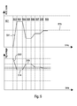
- FIG. 5 An expanded view of a typical sequence of ADC codes 511 and bias voltage signals 512 is illustrated in figure 5 , representing the tuning process corresponding to the second time period 402 in figure 4 , which encompasses a series of successive ADC output code comparison and bias signal tuning steps.
- the bias adjustment module 117 is disabled.
- An initialization signal is provided at the start of a second period 502, causing the module 117 to initialize by setting its output to an initial value, which in the embodiments described above corresponds to a mid-range of the available tuning range. This causes the bias voltage to transition to a first value 514 over the second period 502.
- a comparison is made of the ADC output code, resulting in the output code being found to be greater than the mid-range 513 (corresponding to 2 N-1 for an N bit resolution output).
- the bias voltage is then adjusted to a second value 515 over a fourth period 504. This results in the ADC output code falling below the mid-range value 513 and, following a further comparison step in a fifth period 505, the bias voltage is adjusted again (by a smaller amount) in a sixth period 506, resulting in the ADC code rising and getting closer to the mid-range value 513.
- the tuning process terminates with the ADC output code being close to the mid-range value 513.
Landscapes
- Engineering & Computer Science (AREA)
- Physics & Mathematics (AREA)
- Computer Networks & Wireless Communication (AREA)
- General Physics & Mathematics (AREA)
- Theoretical Computer Science (AREA)
- Signal Processing (AREA)
- Power Engineering (AREA)
- Computer Hardware Design (AREA)
- Microelectronics & Electronic Packaging (AREA)
- Nonlinear Science (AREA)
- General Engineering & Computer Science (AREA)
- Circuits Of Receivers In General (AREA)
Abstract
Description
- The present disclosure relates in general to devices, systems and methods for wireless communication, and in particular to communication using a proximity integrated circuit card (PICC).
- PICCs are widely used for applications where a wireless connection is required between a contactless smart card and a reader. Some uses of such cards include electronic ticketing for public transport, contactless payment for credit and debit cards, and digital identification cards.
- ISO/IEC 14443 is an international standard that defines proximity cards used for identification, together with the associated transmission protocols, and defines such cards in general as proximity integrated circuit cards.
- According to a first aspect of the present disclosure there is provided a circuit for a proximity integrated circuit card, the circuit comprising:
- an input stage having a first input for connection to a radio antenna to receive an input signal, a second input for adjustment of a bias of the input stage and an output for providing a bias adjusted input signal;
- a decoding module connected to the input stage and configured to provide an output code from the bias adjusted input signal; and
- a bias adjustment module connected to receive the output code from the decoding module and configured to provide a bias adjustment signal to the second input of the input stage,
- wherein the bias adjustment module is configured to iteratively tune the bias adjustment signal based on a measurement of the output code, with successive steps tuning the bias adjustment signal by a smaller amount until the output code is within a decoding range.
- The decoding module may have an output resolution of N bits, and the decoding range may include an output of 2N-1.The decoding range may be a single value, for example 2N-1, or may be a range of values within a predetermined number of the single value. The predetermined number may for example be one or two.
- With the bias adjustment module having a resolution of M bits, the bias adjustment module may be configured to initially set the bias adjustment signal at a value corresponding to 2M-1. This corresponds to a bias voltage provided to the input stage in the middle of an available tuning range.
- The bias adjustment module may be configured to increase or decrease the bias adjustment signal by a value corresponding to 2m-2 after initially setting m to be equal to M and to reduce the value of m after each iteration step. The bias adjustment module may, for example, be configured to adjust the bias adjustment signal in a first direction (i.e. to increase or decrease) if the output code is above the decoding range and to adjust the bias adjustment signal in a second opposing direction (i.e. to decrease or increase) if the output code is below the decoding range.
- The bias adjustment module may be configured to stop tuning the bias adjustment signal when the output code reaches or is within the decoding range or when the value of m reaches zero.
- The decoding module may comprise a successive approximation register analog to digital converter.
- The decoding module may be configured to decode an amplitude shift keyed input signal, for example an ASK type B signal.
- According to a second aspect of the present disclosure there is provided a proximity integrated circuit card comprising the circuit according to the first aspect; and an antenna connected to the input stage of the circuit.
- There may be provided a computer program, which when run on a computer, causes the computer to configure the bias adjustment module disclosed herein to perform any method disclosed herein. The computer program may be a software implementation, and the computer may be considered as any appropriate hardware, including a digital signal processor, a microcontroller, and an implementation in read only memory (ROM), erasable programmable read only memory (EPROM) or electronically erasable programmable read only memory (EEPROM), as non-limiting examples. The software implementation may be an assembly program.
- The computer program may be provided on a computer readable medium, which may be a physical computer readable medium, such as a disc or a memory device, or may be embodied as a transient signal. Such a transient signal may be a network download, including an internet download.
- These and other aspects of the invention will be apparent from, and elucidated with reference to, the embodiments described hereinafter.
- Embodiments will be described, by way of example only, with reference to the drawings, in which:
-
figure 1 is a schematic diagram of an exemplary implementation of an ASK type B demodulator and ADC; -
figure 2 is a flow diagram illustrating an exemplary method of bias tuning for the input stage offigure 1 ; -
figure 3 is a schematic diagram of the demodulator and ADC offigure 1 as part of an ASK type B signal path; -
figure 4 is a plot of exemplary ADC output codes and input signal as a function of time; and -
figure 5 is a plot of ADC output codes and bias voltage as a function of time over an exemplary tuning routine. - It should be noted that the Figures are diagrammatic and not drawn to scale. Relative dimensions and proportions of parts of these Figures have been shown exaggerated or reduced in size, for the sake of clarity and convenience in the drawings. The same reference signs are generally used to refer to corresponding or similar feature in modified and different embodiments.
- The ISO/IEC 14443 standard defines that a receiver unit in a PICC should be able to handle an incoming amplitude shift keyed (ASK) type B signal (i.e. with a modulation ratio of <100%) having different data rates, modulation index and field strength while having an ultra-low power consumption and generating a digital output signal for subsequent signal processing. Traditional coherent receiver architectures, such as superheterodyne, direct conversion and low IF architectures, are able to receive and process such signals, but with high power consumption and circuit complexity, neither of which is desirable in a PICC. If a non-coherent receiver is used, this reduces circuit complexity since a carrier recovery circuit is not required. One example of such a receiver is disclosed in
EP2752792 , in which a PLL/DLL free high bandwidth receiver for a type B ISO/IEC 14443 compatible contactless smart card is proposed. This uses an integrate-and-dump filter clocked by a static frequency divider that can be controlled directly by the antenna. - A particular problem with PICC implementations is how to handle incoming signals, for example ASK type B signals, having different data rates, which may range from 106kbps to 6.78 Mbps (over 1 Mbps being generally considered a very high bit rate), a varying modulation index (ranging between 6 and 40% in practical cases, with a typical value around 20%) and over a range of field strengths (typically from 1 A/m to 8 A/m) while maintaining an ultra-low power consumption and small circuit size and maximising the signal dynamic range.
-
Figure 1 illustrates an exemplary implementation of acircuit 100 for receiving and decoding an input signal, as part of a proximity integrated circuit card. Thecircuit 100 comprises aninput stage 101, adecoding module 106 and abias adjustment module 117, thebias adjustment module 117 configured to receive an output code from thedecoding module 106 and provide a bias adjustment signal to theinput stage 101, thebias adjustment module 117 configured to iteratively tune the bias adjustment signal based on a measurement of the output code, with successive steps tuning the bias adjustment signal by a smaller amount until the output code is within a decoding range. - The
input stage 101 has afirst input 102 comprising differential connections LA, LB for connection to a radio antenna for receiving a radio signal. Asecond input 103 is provided for providing a bias voltage Vg to a pair oftransistors bias voltage input 103 connected to the gate of each transistor and the transistor sources connected to the differential antenna inputs LA, LB of thefirst input 102. The drains of thetransistors output 105 for providing a bias adjusted input signal Idc. - The common
gate input stage 101 acts as a full wave rectifier for the signal provided at thefirst input 102, and provides the bias adjusted input signal at theoutput 105 in the form of a current signal Idc. In alternative example embodiments the input stage may comprise a single transistor configured to provide half wave rectification. - The output signal of the
input stage 101 is provided to thedecoding module 106, which is configured to provide an output code ADCout at anoutput 107 of thecircuit 100 from the bias adjusted input signal Idc. In the example embodiment infigure 1 , thedecoding module 106 comprisescurrent mirrors current sources input stage output 105 to a differential signal pair Isrc, Isnk, which is provided to an analog to digital converter (ADC) 113. A differential signal at theinput 102 is thereby converted to a single-ended current Idc by the PMOS differentialcommon gate pair current mirrors EP2752792 . - The first
current mirror 108 provides a mirror of the output signal Idc to a secondcurrent mirror 109. The secondcurrent mirror 109 provides two outputs: a first output being a mirror signal provided to a thirdcurrent mirror 110 and a second output Isrc being a scaled version of the current signal according to a ratio N1:N2. The values of N1 and N2 may be chosen to determine the degree of scaling and thereby to handle different data rates. A higher ratio of N2:N1 (i.e. larger N2 and/or smaller N1) is more applicable for higher data rates. The value of N2 may also be adjusted to provide an automatic gain control (AGC) function for controlling the output signal swing of theADC 113. The thirdcurrent mirror 110 also scales the current according to the ratio N1:N2, and provides a negative version Isnk of the output of the secondcurrent mirror 109. - The
SAR ADC 113 samples the differential input signal provided, and outputs the output code ADCout at thecircuit output 107, the output code being in the form of a series of N-bit words, where N is the resolution of theADC 113. A clock signal is provided to theADC 113 at aclock input 114, the clock signal being provided by an integrate-and-dump typeclock signal generator 115. Theclock signal generator 115 is connected to theinput 102 via anantenna buffer 116, and derives the clock signal from the input signal. An example of an integrate-and-dump type clock signal generator is described further inEP2752792 . - The
bias adjustment module 117 is connected to receive the output code ADCout from theADC 113 and is configured to provide the bias adjustment signal Vg to thesecond input 103 of theinput stage 101. Thebias adjustment module 117, the operation of which is described below in more detail, is configured to iteratively tune the bias adjustment signal Vg based on a measurement of the output code ADCout, in which successive steps involve tuning the bias adjustment signal by a smaller amount until the output code ADCout is within a decoding range. In a typical example, the decoding range is in the mid-range of the ADC output, for example if the ADC output ranges from 0 to 255 (i.e. where N=8), the decoding range would include the value 128, which is in the middle of the output range. In other words, if the resolution of the ADC output is N bits, the decoding range may include an output having a value of 2N-1. The decoding range may, for example have a range of values either side of a preferred mid-range value or alternatively may be a specific single value. - Upon initialization of the
circuit 100, thebias adjustment module 117 may in some example embodiments be configured to initially set the bias adjustment signal Vg at a value corresponding to a mid-range value of the module's output range. For example, if thebias adjustment module 117 is configured to output a signal with a resolution of M bits, themodule 117 may be configured to initially set the bias adjustment signal at a value corresponding to 2M-1. - In the example embodiment of
figure 1 , theADC 113 provides an unsigned output at thecircuit output 107 based on a differential input. Other arrangements may be possible, for example a signed output and/or a single ended input. - The
bias adjustment module 117 may carry out an iterative tuning procedure as outlined in the example flowchart offigure 2 . Upon initialization (step 200), which may be done for example by providing a trigger signal to thebias adjustment module 117, the output code of themodule 117 is initialized as 2M-1, and a starting value of a variable m is set equal to M (step 201). Themodule 117 then checks the ADC output code and compares this to the value of 2N-1 (step 202), which defines the required decoding range mid-way between 0 and 2N for an unsigned output. If the ADC output code is greater than 2N-1, the output code of themodule 117 is increased by 2m-2 (step 203). If, alternatively, the ADC output code is less than 2N-1, the output code of themodule 117 is decreased by 2m-2 (step 204). Depending on the sign of the gain from bias voltage Vg to the ADC output code,step 203 may alternatively implement a decrease and step 204 may implement an increase of the output code ofmodule 117. After eitherstep steps 205, 206), followed by a check to see whether m is equal to one (steps 207, 208). If m=1, the searching process terminates (step 209). If m is not equal to one, the step of checking the ADC output code repeats (step 202). An additional option of proceeding straight to thetermination step 209 may be provided to account for the case where the ADC code is equal to 2N-1. The same effect may, however, be achieved by making one of thebranches joining steps 202 andsteps - The above described bias voltage adaptive tuning method can be used to find the correct biasing voltage vg that results in the maximum ADC output signal range regardless of the field strength of the input signal, which may typically vary from 1 A/m to 8 A/m.
- The field strength may change depending on whether the PICC is moving in relation to the reader, which can result in the field strength changing over the process of initialization. To compensate for this possibility, a DC tracking control may be provided to control the ADC output DC level, for example by gradually updating a previously established code of
module 117 such that the updated value of Vg then brings the ADC output code closer to the desired DC level, so that the output is prevented from clipping. An example DC tracking control algorithm and circuit is described in co-pending European application14192871.3 -
Figure 3 illustrates an example embodiment of an ASK typeB signal path 300 in which a circuit of the type described herein is incorporated. An ASKmodulation signal generator 301 generates a modulated signal, which is received by anantenna model 302, connected to arepresentative load 303. A differential signal LA, LB is provided to an ASKtype B demodulator 304, which provides a differential output signal Isrc, Isnk to an integrate-and-dumptype SAR ADC 305. The demodulator is provided with a regulated voltage supply (vddreg), with an enable signal (En), a clock signal (integrate), an initialization signal (init) and with tuning signals N1, N2, and monitors the output ADC code provided by theADC 305. -
Figure 4 is a plot of a typicalADC output code 411 and LA/LB input 412 as a function of time before, during and after initialization of a circuit according to an example embodiment. During afirst time period 401, the system is being set up while the signal and supply becomes stable. At the end ofperiod 401, the ADC code is clipping at the lower end of its range, making signal reception impossible. After about 200 µs, the bias adjustment module 117 (figure 1 ) is initialized and the adaptive bias tuning procedure (figure 2 ) begins, in asecond time period 402. This procedure may last only a few microseconds before the tuning procedure is complete, and is followed by athird time period 403 of silence before a data signal is transmitted in afourth time period 404. - An expanded view of a typical sequence of
ADC codes 511 and bias voltage signals 512 is illustrated infigure 5 , representing the tuning process corresponding to thesecond time period 402 infigure 4 , which encompasses a series of successive ADC output code comparison and bias signal tuning steps. In afirst period 501, thebias adjustment module 117 is disabled. An initialization signal is provided at the start of asecond period 502, causing themodule 117 to initialize by setting its output to an initial value, which in the embodiments described above corresponds to a mid-range of the available tuning range. This causes the bias voltage to transition to afirst value 514 over thesecond period 502. In athird period 503, a comparison is made of the ADC output code, resulting in the output code being found to be greater than the mid-range 513 (corresponding to 2N-1 for an N bit resolution output). The bias voltage is then adjusted to asecond value 515 over afourth period 504. This results in the ADC output code falling below themid-range value 513 and, following a further comparison step in afifth period 505, the bias voltage is adjusted again (by a smaller amount) in asixth period 506, resulting in the ADC code rising and getting closer to themid-range value 513. After a further tuning cycle inperiods mid-range value 513. - From reading the present disclosure, other variations and modifications will be apparent to the skilled person. Such variations and modifications may involve equivalent and other features which are already known in the art of wireless communication, and which may be used instead of, or in addition to, features already described herein.
- Although the appended claims are directed to particular combinations of features, it should be understood that the scope of the disclosure of the present invention also includes any novel feature or any novel combination of features disclosed herein either explicitly or implicitly or any generalisation thereof, whether or not it relates to the same invention as presently claimed in any claim and whether or not it mitigates any or all of the same technical problems as does the present invention.
- Features which are described in the context of separate embodiments may also be provided in combination in a single embodiment. Conversely, various features which are, for brevity, described in the context of a single embodiment, may also be provided separately or in any suitable sub-combination. The applicant hereby gives notice that new claims may be formulated to such features and/or combinations of such features during the prosecution of the present application or of any further application derived therefrom.
- For the sake of completeness it is also stated that the term "comprising" does not exclude other elements or steps, the term "a" or "an" does not exclude a plurality, a single processor or other unit may fulfil the functions of several means recited in the claims and any reference signs in the claims shall not be construed as limiting the scope of the claims.
Claims (11)
- A circuit for a proximity integrated circuit card, the circuit comprising:an input stage having a first input for connection to a radio antenna to receive an input signal, a second input for adjustment of a bias of the input stage and an output for providing a bias adjusted input signal;a decoding module connected to the input stage and configured to provide an output code from the bias adjusted input signal; anda bias adjustment module connected to receive the output code from the decoding module and configured to provide a bias adjustment signal to the second input of the input stage,wherein the bias adjustment module is configured to iteratively tune the bias adjustment signal based on a measurement of the output code, with successive steps tuning the bias adjustment signal by a smaller amount until the output code is within a decoding range.
- The circuit of claim 1 wherein, with the decoding module having an output resolution of N bits, the decoding range includes an output of 2N-1.
- The circuit of claim 1 or claim 2 wherein, with the bias adjustment module having a resolution of M bits, the bias adjustment module is configured to initially set the bias adjustment signal at a value corresponding to 2M-1.
- The circuit of claim 3 wherein the bias adjustment module is configured to increase or decrease the bias adjustment signal by a value corresponding to 2m-2 after initially setting m to be equal to M and to reduce the value of m after each iteration step.
- The circuit of claim 4 wherein the bias adjustment module is configured to adjust the bias adjustment signal in a first direction if the output code is above the decoding range and to adjust the bias adjustment signal in a second opposing direction if the output code is below the decoding range.
- The circuit of claim 4 or claim 5 wherein the bias adjustment module is configured to stop tuning the bias adjustment signal when the output code is within the decoding range or when the value of m reaches one.
- The circuit of any preceding claim wherein the decoding module comprises a successive approximation register analog to digital converter.
- The circuit of any preceding claim wherein the decoding module is configured to decode an amplitude shift keyed input signal.
- A proximity integrated circuit card comprising:the circuit according to any preceding claim; andan antenna connected to the input stage of the circuit.
- A method of tuning a bias voltage in a circuit according to any of claims 1 to 8 or the proximity integrated circuit card of claim 9, the method comprising the steps of:i) providing a bias adjustment signal to the input stage;ii) comparing an output code from the decoding module with a predetermined tuning range;iii) adjusting the bias adjustment signal by a predetermined amount in dependence on whether the output code is greater or less than the predetermined tuning range; andiv) repeating steps i) to iii) with a reduced predetermined amount until the output code is within the predetermined tuning range.
- A computer program which, when executed, causes a computer to perform the method according to claim 10.
Priority Applications (3)
| Application Number | Priority Date | Filing Date | Title |
|---|---|---|---|
| EP15170536.5A EP3101596B1 (en) | 2015-06-03 | 2015-06-03 | Adaptive bias tuning |
| CN201610334345.XA CN106250942A (en) | 2015-06-03 | 2016-05-19 | Self adaptation Bias runing |
| US15/173,585 US9825788B2 (en) | 2015-06-03 | 2016-06-03 | Adaptive bias tuning |
Applications Claiming Priority (1)
| Application Number | Priority Date | Filing Date | Title |
|---|---|---|---|
| EP15170536.5A EP3101596B1 (en) | 2015-06-03 | 2015-06-03 | Adaptive bias tuning |
Publications (2)
| Publication Number | Publication Date |
|---|---|
| EP3101596A1 true EP3101596A1 (en) | 2016-12-07 |
| EP3101596B1 EP3101596B1 (en) | 2018-04-25 |
Family
ID=53396254
Family Applications (1)
| Application Number | Title | Priority Date | Filing Date |
|---|---|---|---|
| EP15170536.5A Not-in-force EP3101596B1 (en) | 2015-06-03 | 2015-06-03 | Adaptive bias tuning |
Country Status (3)
| Country | Link |
|---|---|
| US (1) | US9825788B2 (en) |
| EP (1) | EP3101596B1 (en) |
| CN (1) | CN106250942A (en) |
Families Citing this family (2)
| Publication number | Priority date | Publication date | Assignee | Title |
|---|---|---|---|---|
| US11469619B2 (en) * | 2020-06-24 | 2022-10-11 | Samsung Electronics Co., Ltd. | Signal power management circuits and smart cards including the same |
| KR102727589B1 (en) * | 2020-06-24 | 2024-11-07 | 삼성전자주식회사 | Signal power management circuit and smart card comprising the same |
Citations (4)
| Publication number | Priority date | Publication date | Assignee | Title |
|---|---|---|---|---|
| EP0942523A1 (en) * | 1998-03-09 | 1999-09-15 | Alps Electric Co., Ltd. | Modulating and demodulating device |
| US20090302935A1 (en) * | 2008-06-10 | 2009-12-10 | Shigeyasu Iwata | Demodulator |
| US7944279B1 (en) * | 2009-12-31 | 2011-05-17 | Nxp B.V. | Charge pump stage of radio-frequency identification transponder |
| EP2752792A1 (en) | 2013-01-08 | 2014-07-09 | Nxp B.V. | Receiver and method for near field communication |
Family Cites Families (31)
| Publication number | Priority date | Publication date | Assignee | Title |
|---|---|---|---|---|
| US3727135A (en) | 1971-04-27 | 1973-04-10 | Us Army | Adaptive code modulation improvement in digital code modulators |
| US5940447A (en) | 1996-08-30 | 1999-08-17 | Motorola, Inc. | Wireless powered communication device using power signal sampling and method |
| US6466007B1 (en) | 2000-08-14 | 2002-10-15 | Teradyne, Inc. | Test system for smart card and indentification devices and the like |
| US6680985B1 (en) | 2000-08-15 | 2004-01-20 | Hughes Electronics Corporation | Adaptive quadrature amplitude modulation decoding system |
| DE10229459C1 (en) | 2002-07-01 | 2003-11-13 | Texas Instruments Deutschland | Transponder for contactless data transmission system has regulation circuit for preventing variation in voltage level of input signal fed from antenna to demodulator |
| US7023817B2 (en) | 2003-03-11 | 2006-04-04 | Motorola, Inc. | Method and apparatus for source device synchronization in a communication system |
| JP4328705B2 (en) | 2004-02-27 | 2009-09-09 | 均 北吉 | RFID tag device |
| JP2006023671A (en) | 2004-07-09 | 2006-01-26 | Sharp Corp | Image forming apparatus and image forming method using the same |
| DE602005023619D1 (en) | 2004-07-13 | 2010-10-28 | Nxp Bv | Demodulator for amplitude modulated signals |
| US20060154599A1 (en) | 2005-01-10 | 2006-07-13 | Faheem Altaf | Systems, methods, and media for providing wireless electronic messaging |
| KR20130069853A (en) | 2005-05-19 | 2013-06-26 | 넥스테스트 시스템즈 코포레이션 | System for testing smart cards and method for same |
| WO2007012053A1 (en) | 2005-07-20 | 2007-01-25 | Stmicroelectronics, S.R.L. | Apparatus and method for detecting communications from multiple sources |
| US8299844B2 (en) * | 2005-09-29 | 2012-10-30 | Case Western Reserve University | System and circuitry to provide stable transconductance for biasing |
| JP4313795B2 (en) | 2005-09-30 | 2009-08-12 | 富士通マイクロエレクトロニクス株式会社 | Non-contact tag, control method of non-contact tag |
| US7691746B2 (en) | 2007-07-31 | 2010-04-06 | Hewlett-Packard Development Company, L.P. | Formation of silicon nitride layer on back side of substrate |
| DE102007036207B4 (en) | 2007-08-02 | 2010-08-12 | Texas Instruments Deutschland Gmbh | Large dynamic range ASK demodulator for use in 13 MHz RFID transponders |
| US7885359B2 (en) | 2007-08-15 | 2011-02-08 | Seiko Epson Corporation | Sampling demodulator for amplitude shift keying (ASK) radio receiver |
| CN101150329B (en) * | 2007-10-16 | 2011-03-16 | 络达科技股份有限公司 | Radio transceiver bias circuit |
| JP4364297B1 (en) | 2008-12-24 | 2009-11-11 | 株式会社東芝 | ASK demodulation circuit, communication module, communication apparatus, and ASK demodulation method |
| US9166533B2 (en) * | 2009-07-30 | 2015-10-20 | Qualcomm Incorporated | Bias current monitor and control mechanism for amplifiers |
| US8222944B2 (en) | 2009-11-20 | 2012-07-17 | Electronics And Telecommunications Research Institute | DC offset cancellation circuit |
| KR20120025747A (en) | 2010-09-08 | 2012-03-16 | 한국전자통신연구원 | Method and apparatus of a passive radio frequency identification reader digital demodulation for manchester subcarrier signal |
| US20120083205A1 (en) | 2010-10-04 | 2012-04-05 | Qualcomm Incorporated | Nfc device having a differential input envelope detector |
| JP5717412B2 (en) | 2010-11-26 | 2015-05-13 | ルネサスエレクトロニクス株式会社 | Semiconductor device for wireless communication |
| US9369120B2 (en) | 2011-01-14 | 2016-06-14 | Infineon Technologies Ag | Detector circuit, transponder and method for detecting signal amplitudes |
| CN103458351B (en) * | 2012-05-31 | 2016-12-14 | 瑞昱半导体股份有限公司 | Composite connector detection circuit and audio codec |
| US9143200B2 (en) | 2012-09-26 | 2015-09-22 | Qualcomm Incorporated | Apparatus and method of receiver architecture and low-complexity decoder for line-coded and amplitude-modulated signal |
| US9819394B2 (en) | 2013-04-29 | 2017-11-14 | MEDIATEX Singapore Pte. Ltd. | Method for controlling an antenna network quality factor of a near field communication device without changing matching network, and associated apparatus |
| CN110557174A (en) | 2013-09-04 | 2019-12-10 | 联发科技(新加坡)私人有限公司 | Envelope extraction device, signal decoding device and short-distance non-contact communication device and related method |
| US9426003B2 (en) | 2013-12-18 | 2016-08-23 | Nxp B.V. | Proximity integrated circuit card bias adjustment |
| CN104268490A (en) | 2014-08-19 | 2015-01-07 | 广东顺德中山大学卡内基梅隆大学国际联合研究院 | RFID card reader |
-
2015
- 2015-06-03 EP EP15170536.5A patent/EP3101596B1/en not_active Not-in-force
-
2016
- 2016-05-19 CN CN201610334345.XA patent/CN106250942A/en not_active Withdrawn
- 2016-06-03 US US15/173,585 patent/US9825788B2/en not_active Expired - Fee Related
Patent Citations (4)
| Publication number | Priority date | Publication date | Assignee | Title |
|---|---|---|---|---|
| EP0942523A1 (en) * | 1998-03-09 | 1999-09-15 | Alps Electric Co., Ltd. | Modulating and demodulating device |
| US20090302935A1 (en) * | 2008-06-10 | 2009-12-10 | Shigeyasu Iwata | Demodulator |
| US7944279B1 (en) * | 2009-12-31 | 2011-05-17 | Nxp B.V. | Charge pump stage of radio-frequency identification transponder |
| EP2752792A1 (en) | 2013-01-08 | 2014-07-09 | Nxp B.V. | Receiver and method for near field communication |
Also Published As
| Publication number | Publication date |
|---|---|
| US20160359648A1 (en) | 2016-12-08 |
| CN106250942A (en) | 2016-12-21 |
| EP3101596B1 (en) | 2018-04-25 |
| US9825788B2 (en) | 2017-11-21 |
Similar Documents
| Publication | Publication Date | Title |
|---|---|---|
| EP2752792B1 (en) | Receiver and method for near field communication | |
| US20190074914A1 (en) | System to calibrate phase using system information | |
| CN110521127B (en) | System and method for peak adaptive sampling demodulation in radio frequency transceivers | |
| CN107735990B (en) | Demodulator circuit and method for demodulation | |
| US10679716B2 (en) | Calibration apparatus and method for sampler with adjustable high frequency gain | |
| US10938107B2 (en) | Circuit and method for driving an antenna of an NFC device | |
| WO2008060672A1 (en) | Peak signal detector | |
| US20080030336A1 (en) | Semiconductor integrated circuit device and receiving device | |
| WO2007121112A2 (en) | Systems, methods and devices for dual closed loop modulation controller for nonlinear rf amplifier | |
| US9594388B2 (en) | Digital shunt regulator for NFC devices | |
| US20150049795A1 (en) | Receiving data compensation method to improve data receiving rate and receiving modem circuit thereof | |
| EP2186279B1 (en) | High dynamic range ask demodulator for use in an rfid transponder | |
| US20140093019A1 (en) | Receiver | |
| US9825788B2 (en) | Adaptive bias tuning | |
| CN110719242A (en) | Equalizer adjustment device, equalizer adjustment method, receiver, and transmission/reception system | |
| CN101657964B (en) | EDGE Power Ramp Using Log Resistor Attenuators | |
| EP2930647B1 (en) | Contactless communication device with receiver input voltage stabilization | |
| KR20150059834A (en) | Reader receiver and reader transmitter and receiver including the same | |
| CN101641927B (en) | Method and apparatus for initial acquisition gain control in a communication system | |
| US20130094562A1 (en) | Transmitter and transmitting method using delay locked loop | |
| EP2887274A1 (en) | Proximity integrated circuit card bias adjustment | |
| US7308239B2 (en) | Receiver for receiving amplitude shift keying signal | |
| CN112511118B (en) | Amplifier and amplification method | |
| CN101208860B (en) | Signal level adjuster , transreceiver for RF communication equipment and RF receiver circuit | |
| CN114629508B (en) | Wave shaping to prevent overshoot and undershoot |
Legal Events
| Date | Code | Title | Description |
|---|---|---|---|
| PUAI | Public reference made under article 153(3) epc to a published international application that has entered the european phase |
Free format text: ORIGINAL CODE: 0009012 |
|
| STAA | Information on the status of an ep patent application or granted ep patent |
Free format text: STATUS: THE APPLICATION HAS BEEN PUBLISHED |
|
| AK | Designated contracting states |
Kind code of ref document: A1 Designated state(s): AL AT BE BG CH CY CZ DE DK EE ES FI FR GB GR HR HU IE IS IT LI LT LU LV MC MK MT NL NO PL PT RO RS SE SI SK SM TR |
|
| AX | Request for extension of the european patent |
Extension state: BA ME |
|
| STAA | Information on the status of an ep patent application or granted ep patent |
Free format text: STATUS: REQUEST FOR EXAMINATION WAS MADE |
|
| 17P | Request for examination filed |
Effective date: 20170607 |
|
| RBV | Designated contracting states (corrected) |
Designated state(s): AL AT BE BG CH CY CZ DE DK EE ES FI FR GB GR HR HU IE IS IT LI LT LU LV MC MK MT NL NO PL PT RO RS SE SI SK SM TR |
|
| GRAP | Despatch of communication of intention to grant a patent |
Free format text: ORIGINAL CODE: EPIDOSNIGR1 |
|
| STAA | Information on the status of an ep patent application or granted ep patent |
Free format text: STATUS: GRANT OF PATENT IS INTENDED |
|
| RIC1 | Information provided on ipc code assigned before grant |
Ipc: H04L 27/06 20060101ALI20180109BHEP Ipc: H03C 7/00 20060101ALI20180109BHEP Ipc: G06K 19/077 20060101AFI20180109BHEP Ipc: H04L 25/06 20060101ALI20180109BHEP Ipc: H04L 27/00 20060101ALI20180109BHEP Ipc: G06K 19/07 20060101ALI20180109BHEP Ipc: H03D 1/18 20060101ALI20180109BHEP |
|
| INTG | Intention to grant announced |
Effective date: 20180125 |
|
| GRAA | (expected) grant |
Free format text: ORIGINAL CODE: 0009210 |
|
| GRAS | Grant fee paid |
Free format text: ORIGINAL CODE: EPIDOSNIGR3 |
|
| STAA | Information on the status of an ep patent application or granted ep patent |
Free format text: STATUS: THE PATENT HAS BEEN GRANTED |
|
| AK | Designated contracting states |
Kind code of ref document: B1 Designated state(s): AL AT BE BG CH CY CZ DE DK EE ES FI FR GB GR HR HU IE IS IT LI LT LU LV MC MK MT NL NO PL PT RO RS SE SI SK SM TR |
|
| REG | Reference to a national code |
Ref country code: GB Ref legal event code: FG4D |
|
| REG | Reference to a national code |
Ref country code: CH Ref legal event code: EP |
|
| REG | Reference to a national code |
Ref country code: AT Ref legal event code: REF Ref document number: 993655 Country of ref document: AT Kind code of ref document: T Effective date: 20180515 |
|
| REG | Reference to a national code |
Ref country code: IE Ref legal event code: FG4D |
|
| REG | Reference to a national code |
Ref country code: DE Ref legal event code: R096 Ref document number: 602015010303 Country of ref document: DE |
|
| REG | Reference to a national code |
Ref country code: FR Ref legal event code: PLFP Year of fee payment: 4 |
|
| REG | Reference to a national code |
Ref country code: NL Ref legal event code: MP Effective date: 20180425 |
|
| REG | Reference to a national code |
Ref country code: LT Ref legal event code: MG4D |
|
| PG25 | Lapsed in a contracting state [announced via postgrant information from national office to epo] |
Ref country code: NL Free format text: LAPSE BECAUSE OF FAILURE TO SUBMIT A TRANSLATION OF THE DESCRIPTION OR TO PAY THE FEE WITHIN THE PRESCRIBED TIME-LIMIT Effective date: 20180425 |
|
| PG25 | Lapsed in a contracting state [announced via postgrant information from national office to epo] |
Ref country code: ES Free format text: LAPSE BECAUSE OF FAILURE TO SUBMIT A TRANSLATION OF THE DESCRIPTION OR TO PAY THE FEE WITHIN THE PRESCRIBED TIME-LIMIT Effective date: 20180425 Ref country code: SE Free format text: LAPSE BECAUSE OF FAILURE TO SUBMIT A TRANSLATION OF THE DESCRIPTION OR TO PAY THE FEE WITHIN THE PRESCRIBED TIME-LIMIT Effective date: 20180425 Ref country code: PL Free format text: LAPSE BECAUSE OF FAILURE TO SUBMIT A TRANSLATION OF THE DESCRIPTION OR TO PAY THE FEE WITHIN THE PRESCRIBED TIME-LIMIT Effective date: 20180425 Ref country code: LT Free format text: LAPSE BECAUSE OF FAILURE TO SUBMIT A TRANSLATION OF THE DESCRIPTION OR TO PAY THE FEE WITHIN THE PRESCRIBED TIME-LIMIT Effective date: 20180425 Ref country code: BG Free format text: LAPSE BECAUSE OF FAILURE TO SUBMIT A TRANSLATION OF THE DESCRIPTION OR TO PAY THE FEE WITHIN THE PRESCRIBED TIME-LIMIT Effective date: 20180725 Ref country code: NO Free format text: LAPSE BECAUSE OF FAILURE TO SUBMIT A TRANSLATION OF THE DESCRIPTION OR TO PAY THE FEE WITHIN THE PRESCRIBED TIME-LIMIT Effective date: 20180725 Ref country code: FI Free format text: LAPSE BECAUSE OF FAILURE TO SUBMIT A TRANSLATION OF THE DESCRIPTION OR TO PAY THE FEE WITHIN THE PRESCRIBED TIME-LIMIT Effective date: 20180425 |
|
| PG25 | Lapsed in a contracting state [announced via postgrant information from national office to epo] |
Ref country code: GR Free format text: LAPSE BECAUSE OF FAILURE TO SUBMIT A TRANSLATION OF THE DESCRIPTION OR TO PAY THE FEE WITHIN THE PRESCRIBED TIME-LIMIT Effective date: 20180726 Ref country code: RS Free format text: LAPSE BECAUSE OF FAILURE TO SUBMIT A TRANSLATION OF THE DESCRIPTION OR TO PAY THE FEE WITHIN THE PRESCRIBED TIME-LIMIT Effective date: 20180425 Ref country code: LV Free format text: LAPSE BECAUSE OF FAILURE TO SUBMIT A TRANSLATION OF THE DESCRIPTION OR TO PAY THE FEE WITHIN THE PRESCRIBED TIME-LIMIT Effective date: 20180425 Ref country code: HR Free format text: LAPSE BECAUSE OF FAILURE TO SUBMIT A TRANSLATION OF THE DESCRIPTION OR TO PAY THE FEE WITHIN THE PRESCRIBED TIME-LIMIT Effective date: 20180425 |
|
| REG | Reference to a national code |
Ref country code: AT Ref legal event code: MK05 Ref document number: 993655 Country of ref document: AT Kind code of ref document: T Effective date: 20180425 |
|
| PG25 | Lapsed in a contracting state [announced via postgrant information from national office to epo] |
Ref country code: PT Free format text: LAPSE BECAUSE OF FAILURE TO SUBMIT A TRANSLATION OF THE DESCRIPTION OR TO PAY THE FEE WITHIN THE PRESCRIBED TIME-LIMIT Effective date: 20180827 |
|
| REG | Reference to a national code |
Ref country code: DE Ref legal event code: R097 Ref document number: 602015010303 Country of ref document: DE |
|
| PG25 | Lapsed in a contracting state [announced via postgrant information from national office to epo] |
Ref country code: CZ Free format text: LAPSE BECAUSE OF FAILURE TO SUBMIT A TRANSLATION OF THE DESCRIPTION OR TO PAY THE FEE WITHIN THE PRESCRIBED TIME-LIMIT Effective date: 20180425 Ref country code: SK Free format text: LAPSE BECAUSE OF FAILURE TO SUBMIT A TRANSLATION OF THE DESCRIPTION OR TO PAY THE FEE WITHIN THE PRESCRIBED TIME-LIMIT Effective date: 20180425 Ref country code: EE Free format text: LAPSE BECAUSE OF FAILURE TO SUBMIT A TRANSLATION OF THE DESCRIPTION OR TO PAY THE FEE WITHIN THE PRESCRIBED TIME-LIMIT Effective date: 20180425 Ref country code: DK Free format text: LAPSE BECAUSE OF FAILURE TO SUBMIT A TRANSLATION OF THE DESCRIPTION OR TO PAY THE FEE WITHIN THE PRESCRIBED TIME-LIMIT Effective date: 20180425 Ref country code: AT Free format text: LAPSE BECAUSE OF FAILURE TO SUBMIT A TRANSLATION OF THE DESCRIPTION OR TO PAY THE FEE WITHIN THE PRESCRIBED TIME-LIMIT Effective date: 20180425 Ref country code: RO Free format text: LAPSE BECAUSE OF FAILURE TO SUBMIT A TRANSLATION OF THE DESCRIPTION OR TO PAY THE FEE WITHIN THE PRESCRIBED TIME-LIMIT Effective date: 20180425 |
|
| REG | Reference to a national code |
Ref country code: CH Ref legal event code: PL |
|
| PG25 | Lapsed in a contracting state [announced via postgrant information from national office to epo] |
Ref country code: IT Free format text: LAPSE BECAUSE OF FAILURE TO SUBMIT A TRANSLATION OF THE DESCRIPTION OR TO PAY THE FEE WITHIN THE PRESCRIBED TIME-LIMIT Effective date: 20180425 Ref country code: SM Free format text: LAPSE BECAUSE OF FAILURE TO SUBMIT A TRANSLATION OF THE DESCRIPTION OR TO PAY THE FEE WITHIN THE PRESCRIBED TIME-LIMIT Effective date: 20180425 |
|
| PLBE | No opposition filed within time limit |
Free format text: ORIGINAL CODE: 0009261 |
|
| STAA | Information on the status of an ep patent application or granted ep patent |
Free format text: STATUS: NO OPPOSITION FILED WITHIN TIME LIMIT |
|
| REG | Reference to a national code |
Ref country code: BE Ref legal event code: MM Effective date: 20180630 |
|
| REG | Reference to a national code |
Ref country code: IE Ref legal event code: MM4A |
|
| PG25 | Lapsed in a contracting state [announced via postgrant information from national office to epo] |
Ref country code: MC Free format text: LAPSE BECAUSE OF FAILURE TO SUBMIT A TRANSLATION OF THE DESCRIPTION OR TO PAY THE FEE WITHIN THE PRESCRIBED TIME-LIMIT Effective date: 20180425 Ref country code: LU Free format text: LAPSE BECAUSE OF NON-PAYMENT OF DUE FEES Effective date: 20180603 |
|
| 26N | No opposition filed |
Effective date: 20190128 |
|
| PG25 | Lapsed in a contracting state [announced via postgrant information from national office to epo] |
Ref country code: LI Free format text: LAPSE BECAUSE OF NON-PAYMENT OF DUE FEES Effective date: 20180630 Ref country code: CH Free format text: LAPSE BECAUSE OF NON-PAYMENT OF DUE FEES Effective date: 20180630 Ref country code: IE Free format text: LAPSE BECAUSE OF NON-PAYMENT OF DUE FEES Effective date: 20180603 |
|
| PG25 | Lapsed in a contracting state [announced via postgrant information from national office to epo] |
Ref country code: BE Free format text: LAPSE BECAUSE OF NON-PAYMENT OF DUE FEES Effective date: 20180630 Ref country code: SI Free format text: LAPSE BECAUSE OF FAILURE TO SUBMIT A TRANSLATION OF THE DESCRIPTION OR TO PAY THE FEE WITHIN THE PRESCRIBED TIME-LIMIT Effective date: 20180425 |
|
| PGFP | Annual fee paid to national office [announced via postgrant information from national office to epo] |
Ref country code: DE Payment date: 20190521 Year of fee payment: 5 |
|
| PGFP | Annual fee paid to national office [announced via postgrant information from national office to epo] |
Ref country code: FR Payment date: 20190522 Year of fee payment: 5 |
|
| PGFP | Annual fee paid to national office [announced via postgrant information from national office to epo] |
Ref country code: GB Payment date: 20190522 Year of fee payment: 5 |
|
| PG25 | Lapsed in a contracting state [announced via postgrant information from national office to epo] |
Ref country code: AL Free format text: LAPSE BECAUSE OF FAILURE TO SUBMIT A TRANSLATION OF THE DESCRIPTION OR TO PAY THE FEE WITHIN THE PRESCRIBED TIME-LIMIT Effective date: 20180425 |
|
| PG25 | Lapsed in a contracting state [announced via postgrant information from national office to epo] |
Ref country code: MT Free format text: LAPSE BECAUSE OF NON-PAYMENT OF DUE FEES Effective date: 20180603 |
|
| PG25 | Lapsed in a contracting state [announced via postgrant information from national office to epo] |
Ref country code: TR Free format text: LAPSE BECAUSE OF FAILURE TO SUBMIT A TRANSLATION OF THE DESCRIPTION OR TO PAY THE FEE WITHIN THE PRESCRIBED TIME-LIMIT Effective date: 20180425 |
|
| PG25 | Lapsed in a contracting state [announced via postgrant information from national office to epo] |
Ref country code: HU Free format text: LAPSE BECAUSE OF FAILURE TO SUBMIT A TRANSLATION OF THE DESCRIPTION OR TO PAY THE FEE WITHIN THE PRESCRIBED TIME-LIMIT; INVALID AB INITIO Effective date: 20150603 Ref country code: CY Free format text: LAPSE BECAUSE OF FAILURE TO SUBMIT A TRANSLATION OF THE DESCRIPTION OR TO PAY THE FEE WITHIN THE PRESCRIBED TIME-LIMIT Effective date: 20180425 Ref country code: MK Free format text: LAPSE BECAUSE OF NON-PAYMENT OF DUE FEES Effective date: 20180425 |
|
| PG25 | Lapsed in a contracting state [announced via postgrant information from national office to epo] |
Ref country code: IS Free format text: LAPSE BECAUSE OF FAILURE TO SUBMIT A TRANSLATION OF THE DESCRIPTION OR TO PAY THE FEE WITHIN THE PRESCRIBED TIME-LIMIT Effective date: 20180825 |
|
| REG | Reference to a national code |
Ref country code: DE Ref legal event code: R119 Ref document number: 602015010303 Country of ref document: DE |
|
| GBPC | Gb: european patent ceased through non-payment of renewal fee |
Effective date: 20200603 |
|
| PG25 | Lapsed in a contracting state [announced via postgrant information from national office to epo] |
Ref country code: FR Free format text: LAPSE BECAUSE OF NON-PAYMENT OF DUE FEES Effective date: 20200630 Ref country code: GB Free format text: LAPSE BECAUSE OF NON-PAYMENT OF DUE FEES Effective date: 20200603 |
|
| PG25 | Lapsed in a contracting state [announced via postgrant information from national office to epo] |
Ref country code: DE Free format text: LAPSE BECAUSE OF NON-PAYMENT OF DUE FEES Effective date: 20210101 |