EP3101438A1 - Jitter control circuit within chip and associated jitter control method - Google Patents
Jitter control circuit within chip and associated jitter control method Download PDFInfo
- Publication number
- EP3101438A1 EP3101438A1 EP16167532.7A EP16167532A EP3101438A1 EP 3101438 A1 EP3101438 A1 EP 3101438A1 EP 16167532 A EP16167532 A EP 16167532A EP 3101438 A1 EP3101438 A1 EP 3101438A1
- Authority
- EP
- European Patent Office
- Prior art keywords
- pdn
- adaptive
- jitter
- control circuit
- current
- Prior art date
- Legal status (The legal status is an assumption and is not a legal conclusion. Google has not performed a legal analysis and makes no representation as to the accuracy of the status listed.)
- Granted
Links
Images
Classifications
-
- H—ELECTRICITY
- H02—GENERATION; CONVERSION OR DISTRIBUTION OF ELECTRIC POWER
- H02M—APPARATUS FOR CONVERSION BETWEEN AC AND AC, BETWEEN AC AND DC, OR BETWEEN DC AND DC, AND FOR USE WITH MAINS OR SIMILAR POWER SUPPLY SYSTEMS; CONVERSION OF DC OR AC INPUT POWER INTO SURGE OUTPUT POWER; CONTROL OR REGULATION THEREOF
- H02M3/00—Conversion of DC power input into DC power output
-
- H—ELECTRICITY
- H03—ELECTRONIC CIRCUITRY
- H03L—AUTOMATIC CONTROL, STARTING, SYNCHRONISATION OR STABILISATION OF GENERATORS OF ELECTRONIC OSCILLATIONS OR PULSES
- H03L1/00—Stabilisation of generator output against variations of physical values, e.g. power supply
-
- G—PHYSICS
- G01—MEASURING; TESTING
- G01R—MEASURING ELECTRIC VARIABLES; MEASURING MAGNETIC VARIABLES
- G01R31/00—Arrangements for testing electric properties; Arrangements for locating electric faults; Arrangements for electrical testing characterised by what is being tested not provided for elsewhere
- G01R31/28—Testing of electronic circuits, e.g. by signal tracer
- G01R31/317—Testing of digital circuits
- G01R31/31708—Analysis of signal quality
- G01R31/31709—Jitter measurements; Jitter generators
-
- H—ELECTRICITY
- H02—GENERATION; CONVERSION OR DISTRIBUTION OF ELECTRIC POWER
- H02M—APPARATUS FOR CONVERSION BETWEEN AC AND AC, BETWEEN AC AND DC, OR BETWEEN DC AND DC, AND FOR USE WITH MAINS OR SIMILAR POWER SUPPLY SYSTEMS; CONVERSION OF DC OR AC INPUT POWER INTO SURGE OUTPUT POWER; CONTROL OR REGULATION THEREOF
- H02M3/00—Conversion of DC power input into DC power output
- H02M3/02—Conversion of DC power input into DC power output without intermediate conversion into AC
- H02M3/04—Conversion of DC power input into DC power output without intermediate conversion into AC by static converters
- H02M3/10—Conversion of DC power input into DC power output without intermediate conversion into AC by static converters using discharge tubes with control electrode or semiconductor devices with control electrode
- H02M3/145—Conversion of DC power input into DC power output without intermediate conversion into AC by static converters using discharge tubes with control electrode or semiconductor devices with control electrode using devices of a triode or transistor type requiring continuous application of a control signal
- H02M3/155—Conversion of DC power input into DC power output without intermediate conversion into AC by static converters using discharge tubes with control electrode or semiconductor devices with control electrode using devices of a triode or transistor type requiring continuous application of a control signal using semiconductor devices only
-
- H—ELECTRICITY
- H03—ELECTRONIC CIRCUITRY
- H03L—AUTOMATIC CONTROL, STARTING, SYNCHRONISATION OR STABILISATION OF GENERATORS OF ELECTRONIC OSCILLATIONS OR PULSES
- H03L7/00—Automatic control of frequency or phase; Synchronisation
-
- H—ELECTRICITY
- H04—ELECTRIC COMMUNICATION TECHNIQUE
- H04L—TRANSMISSION OF DIGITAL INFORMATION, e.g. TELEGRAPHIC COMMUNICATION
- H04L7/00—Arrangements for synchronising receiver with transmitter
- H04L7/0079—Receiver details
- H04L7/0087—Preprocessing of received signal for synchronisation, e.g. by code conversion, pulse generation or edge detection
-
- H—ELECTRICITY
- H04—ELECTRIC COMMUNICATION TECHNIQUE
- H04L—TRANSMISSION OF DIGITAL INFORMATION, e.g. TELEGRAPHIC COMMUNICATION
- H04L7/00—Arrangements for synchronising receiver with transmitter
- H04L7/04—Speed or phase control by synchronisation signals
- H04L7/06—Speed or phase control by synchronisation signals the synchronisation signals differing from the information signals in amplitude, polarity or frequency or length
- H04L7/065—Speed or phase control by synchronisation signals the synchronisation signals differing from the information signals in amplitude, polarity or frequency or length and superimposed by modulation
-
- H—ELECTRICITY
- H02—GENERATION; CONVERSION OR DISTRIBUTION OF ELECTRIC POWER
- H02M—APPARATUS FOR CONVERSION BETWEEN AC AND AC, BETWEEN AC AND DC, OR BETWEEN DC AND DC, AND FOR USE WITH MAINS OR SIMILAR POWER SUPPLY SYSTEMS; CONVERSION OF DC OR AC INPUT POWER INTO SURGE OUTPUT POWER; CONTROL OR REGULATION THEREOF
- H02M1/00—Details of apparatus for conversion
- H02M1/0003—Details of control, feedback or regulation circuits
-
- H—ELECTRICITY
- H02—GENERATION; CONVERSION OR DISTRIBUTION OF ELECTRIC POWER
- H02M—APPARATUS FOR CONVERSION BETWEEN AC AND AC, BETWEEN AC AND DC, OR BETWEEN DC AND DC, AND FOR USE WITH MAINS OR SIMILAR POWER SUPPLY SYSTEMS; CONVERSION OF DC OR AC INPUT POWER INTO SURGE OUTPUT POWER; CONTROL OR REGULATION THEREOF
- H02M1/00—Details of apparatus for conversion
- H02M1/0003—Details of control, feedback or regulation circuits
- H02M1/0038—Circuits or arrangements for suppressing, e.g. by masking incorrect turn-on or turn-off signals, e.g. due to current spikes in current mode control
Definitions
- the external supply voltage is inputted into the chip via a power delivery network (PDN) including many connections such as printed circuit board (PCB) routing, substrate traces, wire bond, input/output pad and internal metal layer etc.
- PDN power delivery network
- the PDN can be modeled as a RLC circuit consisting of a resistor, an inductor and a capacitor, and impedance of the PDN varies with a frequency thereon.
- the chip also includes a plurality of drivers that may sink currents from the PDN, the current generated by the drivers and the impedance of the PDN form a supply voltage noise on the PDN.
- This supply voltage noise may cause a clock generator within the chip to generate a clock with serious jitter. Therefore, providing a scheme to reduce this power supply induced jitter (PSIJ) is an important topic.
- PSIJ power supply induced jitter
- a jitter control circuit within a chip comprises an adaptive PDN, a current generator and a jitter generator.
- the adaptive PDN is capable of being controlled/modulated to provide difference impedances.
- the current generator is coupled to the adaptive PDN, and is arranged for receiving a supply voltage provided by the adaptive PDN and generating currents with different patterns.
- the jitter generator is coupled to the adaptive PDN, and is arranged for generating a plurality of jitters corresponding to the currents with different patterns, respectively, according to the supply voltage provided by the adaptive PDN.
- a jitter control method comprises: providing an adaptive PDN capable of being controlled/modulated to provide difference impedances; receiving a supply voltage provided by the adaptive PDN and generating currents with different patterns; and generating a plurality of jitters corresponding to the currents with different patterns, respectively, according to the supply voltage provided by the adaptive PDN.
- a jitter control circuit within a chip comprises an adaptive PDN, a current generator and a controller.
- the adaptive PDN is capable of being controlled/modulated to provide difference impedances.
- the current generator is coupled to the adaptive PDN, and is arranged for receiving a supply voltage provided by the adaptive PDN and generating a current.
- the controller is coupled to the adaptive PDN and the current generator, and is arranged for controlling the impedance of the adaptive PDN according to a pattern of the current generated by the current generator.
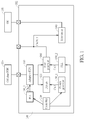
- FIG. 1 is a diagram illustrating a jitter control circuit 100 according to one embodiment of the present invention.
- the jitter control circuit 100 is within a chip 102, and the jitter control circuit 100 comprises an adaptive power delivery network (PDN) 110, a current generator (in this embodiment, the current generator is implemented by a plurality of drivers 120), a controller 130, a jitter meter 140, a pattern generator 150_1 (in this embodiment, the pattern generator 150_1 may be implemented by a phase-locked loop (PLL)), two PLL 150_2 and 150_3 and a jitter generator 160.
- PDN adaptive power delivery network
- the current generator is implemented by a plurality of drivers 120
- a controller 130 a jitter meter 140
- a pattern generator 150_1 in this embodiment, the pattern generator 150_1 may be implemented by a phase-locked loop (PLL)
- PLL phase-locked loop
- the adaptive PDN 110 is coupled to an off-chip PDN 104
- the off-chip PDN 104 is coupled to an external power supply, and is arranged to provide a supply voltage to the adaptive PDN 110 of the chip 102, and the adaptive PDN 110 provides the received supply voltage to the drivers 1 20 and the jitter generator 160 and other elements required using the supply voltage.
- the drivers 120 can be any functional circuit elements that may provide or sink current according to the supply voltage.
- the jitter generator 160 is arranged to output an output clock CKOUT based on a clock CK2 provided by the PLL 150_2 and the supply voltage.
- the pattern generator 150_1 is arranged to provide a clock CK1 to the drivers 1 20 to control the pattern of the current (hereinafter, the frequency serves as an example of the pattern) generated by the drivers 120; and the PLL 150_3 is arranged to generate a clock CK3 to control the frequency of the adaptive PDN 110 to determine the impedance of the adaptive PDN 110.
- a jitter level of the output clock CKOUT is determined based on the impedance of the off-chip PDN 104, the adaptive PDN 110, the frequency of the current of the drivers 120 and the sensitivity of the clock CK2.
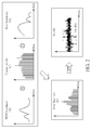
- the jitter J(f) of the output clock CKOUT can be obtained by the product of the impedance of the off-chip PDN 104 and the adaptive PDN 110 (Z(f)), the current I(f) of the drivers 120 and the sensitivity S(f) of the clock CK2, and
- FIG. 2 shows a diagram of the peak-to-peak jitter (p-p jitter) when the jitter J(f) is transformed to time domain by using iFFT (inverse fast Fourier transform).
- the jitter control circuit 100 may provide different operations during an off-line period and an on-line period.
- the jitter control circuit 100 is arranged to control frequencies of the pattern generator 150_1 and the PLL 150_3 to find some particular combinations of the frequencies of the pattern generator 150_1 and the PLL 150_3, where the particular combinations may correspond to serious jitter of an output clock CKOUT outputted by the jitter generator 160, the slight jitter of an output clock CKOUT outputted by the jitter generator 1 60, and/or any other required jitter information.
- the controller 130 may refer to the look-up table to adjust the impedance of the adaptive PDN 110 according to the frequency of the current generated by the drivers 120 and/or other drivers, so as to lower the jitter of the output clock CKOUT outputted by the jitter generator 1 60 or to lower the jitter of the other clock(s).
- the operations of the jitter control circuit 100 are provided below.
- the controller 130 controls the PLL 150_2 to output the clock CK2 with a fixed frequency, then the controller 130 controls the pattern generator 150_1 to output the clock CK1 with different frequencies to the drivers 120 to make the current have different frequencies respectively, and the controller 130 controls the PLL 150_3 to output the clock CK3 for modulating the adaptive PDN 110 to have different frequencies to have different values of impedance respectively.
- the controller 130 controls the PLL 150_2 to output the clock CK2 with a fixed frequency
- the controller 130 controls the pattern generator 150_1 to output the clock CK1 with different frequencies to the drivers 120 to make the current have different frequencies respectively
- the controller 130 controls the PLL 150_3 to output the clock CK3 for modulating the adaptive PDN 110 to have different frequencies to have different values of impedance respectively.
- a corresponding supply voltage noise is generated on the metal routing within the chip 102, causing different jitter level of the output clock CKOUT.
- the jitter meter 140 determines the jitter level of the output clock CKOUT corresponding to every combination of the frequencies of the clocks CK1 and CK3 to generate a plurality of determining results, and sends the determining results to the software side 106.
- the controller 130 may control the PLL 150_3 to output the clock CK3 to modulate the adaptive PDN 110 to have a specific frequency to have a specific impedance, then the controller 130 controls the pattern generator 150_1 to output the clock CK1 with different frequencies to the drivers 120 to make the current to have different frequencies, respectively, and the jitter meter 140 determines the jitter levels of the output clock CKOUT corresponding to the different frequencies of clock CK1 (i.e. different frequencies of the current) respectively.
- the controller 130 controls the PLL 150_3 to output the clock CK3 to modulate the adaptive PDN 110 to have the different impedances, respectively, and the jitter meter 140 determines the jitter levels of the output clock CKOUT corresponding to the combinations of the current with the portion of the frequencies and the different frequencies of the adaptive PDN 110, respectively.
- the controller 130 may fix the clock CK1 with 300 MHz and control the PLL 150_3 to output the clock CK3 to have many different frequencies to find a combination of the frequencies of the clocks CK1 and CK3 corresponding to a slight jitter, for example the clock CK3 with 2 GHz; and the controller 130 may further fix the clock CK1 with 1 GHz and control the PLL 150_3 to output the clock CK3 to have many different frequencies to find a combination of the frequencies of the clocks CK1 and CK3 corresponding to a slight jitter, for example the clock CK3 with 1.5 GHz.
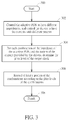
- FIG. 3 The operations of the jitter control circuit 100 during the off-line period are summarized as shown in FIG. 3 .
- the flow of the jitter control method during the off-line period is as follows:
- the controller 1 30 may refer to the look-up table to adjust the impedance of the adaptive PDN 110 according to the frequency of the current generated by the drivers 120 and/or other drivers, so as to lower the jitter of the output clock CKOUT or the other clock signals.
- the controller 130 detects that the current of the drivers within the chip 102 has the frequency close to or equal to 300MHz
- the controller 130 detects whether the impedance/frequency of the adaptive PDN 110 causes a clock jitter while the frequency of the current of the drivers is 300 MHz.
- the controller 130 determines that the impedance/frequency of the adaptive PDN 110 causes the serious clock jitter (e.g. the frequency of the adaptive PDN 110 is 1 GHz)
- the controller 130 will search for an appropriate frequency of the adaptive PDN 110 in the look-up table to lower the clock jitter, for example, 2 GHz, and controls the PLL 150_3 to output the clock CK3 with the frequency 2 GHz.
- the controller 130 determines that the impedance/frequency of the adaptive PDN 110 does not cause the serious clock jitter (e.g. the frequency of the adaptive PDN 110 is close to 2 GHz)
- the adaptive PDN 110 will not adjust the frequency of the clock CK3.
- the drivers 120 can be implemented by a simultaneous Switching Output (SSO) noise generator for generating the current noise according to the supply voltage provided by the adaptive PDN 110
- the jitter generator 160 can be implemented by D-type flip-flops supplied by the supply voltage provided by the adaptive PDN 110 to receive the clock CK2 to generate the output clock CKOUT
- the adaptive PDN 110 can be implemented by any type of circuits such as switched capacitors or any other RLC circuit whose impedance is varied with the frequency of the signal applied thereon, without limitations of the present invention.
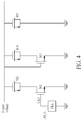
- FIG. 4 is a diagram illustrating the adaptive PDN 110 according to one embodiment of the present invention.
- the adaptive PDN 110 comprises five transistors M1-M5, and is modulated by the clock CK3.
- the adaptive PDN 110 is provided to adjust its own impedance to lower the clock jitter within the chip 102, and the look-up table for adjusting the impedance of the adaptive PDN 110 is built based on the jitters generated based on the internal circuits within the chip 102. Therefore, the information of the look-up table is more reliable, and the impedance of the adaptive PDN 110 can be controlled to effectively lower the clock jitter.
Landscapes
- Engineering & Computer Science (AREA)
- Physics & Mathematics (AREA)
- Computer Networks & Wireless Communication (AREA)
- Signal Processing (AREA)
- Nonlinear Science (AREA)
- General Engineering & Computer Science (AREA)
- General Physics & Mathematics (AREA)
- Power Engineering (AREA)
- Stabilization Of Oscillater, Synchronisation, Frequency Synthesizers (AREA)
- Manipulation Of Pulses (AREA)
Abstract
Description
- For a chip supplied by an external supply voltage, the external supply voltage is inputted into the chip via a power delivery network (PDN) including many connections such as printed circuit board (PCB) routing, substrate traces, wire bond, input/output pad and internal metal layer etc.. The PDN can be modeled as a RLC circuit consisting of a resistor, an inductor and a capacitor, and impedance of the PDN varies with a frequency thereon. In addition, because the chip also includes a plurality of drivers that may sink currents from the PDN, the current generated by the drivers and the impedance of the PDN form a supply voltage noise on the PDN. This supply voltage noise may cause a clock generator within the chip to generate a clock with serious jitter. Therefore, providing a scheme to reduce this power supply induced jitter (PSIJ) is an important topic.
- It is therefore an objective of the present invention to provide a Jitter control circuit and associated jitter control method to effectively reduce the power supply induced jitter, to solve the above-mentioned problem.
- This is achieved by a jitter control circuit according to claim 1, a jitter control method according to claim 7, and a jitter control circuit to claim 13. The dependent claims pertain to corresponding further developments and improvements.
- As will be seen more clearly from the detailed description following below, a jitter control circuit within a chip comprises an adaptive PDN, a current generator and a jitter generator. The adaptive PDN is capable of being controlled/modulated to provide difference impedances. The current generator is coupled to the adaptive PDN, and is arranged for receiving a supply voltage provided by the adaptive PDN and generating currents with different patterns. The jitter generator is coupled to the adaptive PDN, and is arranged for generating a plurality of jitters corresponding to the currents with different patterns, respectively, according to the supply voltage provided by the adaptive PDN.
- As will be seen more clearly from the detailed description following below, a jitter control method comprises: providing an adaptive PDN capable of being controlled/modulated to provide difference impedances; receiving a supply voltage provided by the adaptive PDN and generating currents with different patterns; and generating a plurality of jitters corresponding to the currents with different patterns, respectively, according to the supply voltage provided by the adaptive PDN.
- As will be seen more clearly from the detailed description following below, a jitter control circuit within a chip comprises an adaptive PDN, a current generator and a controller. The adaptive PDN is capable of being controlled/modulated to provide difference impedances. The current generator is coupled to the adaptive PDN, and is arranged for receiving a supply voltage provided by the adaptive PDN and generating a current. The controller is coupled to the adaptive PDN and the current generator, and is arranged for controlling the impedance of the adaptive PDN according to a pattern of the current generated by the current generator.
- These and other objectives of the present invention will no doubt become obvious to those of ordinary skill in the art after reading the following detailed description of the preferred embodiment that is illustrated in the various figures and drawings.
-
-
FIG. 1 is a diagram illustrating a jitter control circuit according to one embodiment of the present invention. -
FIG. 2 shows a diagram illustrating a generation of the jitter. -
FIG. 3 is a flowchart of a jitter control method according to one embodiment of the present invention. -
FIG. 4 is a diagram illustrating an adaptive PDN according to one embodiment of the present invention. - Certain terms are used throughout the following description and claims to refer to particular system components. As one skilled in the art will appreciate, manufacturers may refer to a component by different names. This document does not intend to distinguish between components that differ in name but not function. In the following discussion and in the claims, the terms "including" and "comprising" are used in an open-ended fashion, and thus should be interpreted to mean "including, but not limited to ..." The terms "couple" and "couples" are intended to mean either an indirect or a direct electrical connection. Thus, if a first device couples to a second device, that connection may be through a direct electrical connection, or through an indirect electrical connection via other devices and connections.
- Please refer to
FIG. 1 , which is a diagram illustrating ajitter control circuit 100 according to one embodiment of the present invention. As shown inFIG. 1 , thejitter control circuit 100 is within achip 102, and thejitter control circuit 100 comprises an adaptive power delivery network (PDN) 110, a current generator (in this embodiment, the current generator is implemented by a plurality of drivers 120), acontroller 130, ajitter meter 140, a pattern generator 150_1 (in this embodiment, the pattern generator 150_1 may be implemented by a phase-locked loop (PLL)), two PLL 150_2 and 150_3 and ajitter generator 160. In addition, theadaptive PDN 110 is coupled to an off-chip PDN 104, and thejitter meter 140 is coupled to asoftware side 106. - In this embodiment, the off-
chip PDN 104 is coupled to an external power supply, and is arranged to provide a supply voltage to theadaptive PDN 110 of thechip 102, and theadaptive PDN 110 provides the received supply voltage to the drivers 1 20 and thejitter generator 160 and other elements required using the supply voltage. Thedrivers 120 can be any functional circuit elements that may provide or sink current according to the supply voltage. Thejitter generator 160 is arranged to output an output clock CKOUT based on a clock CK2 provided by the PLL 150_2 and the supply voltage. The pattern generator 150_1 is arranged to provide a clock CK1 to the drivers 1 20 to control the pattern of the current (hereinafter, the frequency serves as an example of the pattern) generated by thedrivers 120; and the PLL 150_3 is arranged to generate a clock CK3 to control the frequency of theadaptive PDN 110 to determine the impedance of theadaptive PDN 110. - In
FIG. 1 , a jitter level of the output clock CKOUT is determined based on the impedance of the off-chip PDN 104, theadaptive PDN 110, the frequency of the current of thedrivers 120 and the sensitivity of the clock CK2. In detail, refer toFIG. 2 , the jitter J(f) of the output clock CKOUT can be obtained by the product of the impedance of the off-chip PDN 104 and the adaptive PDN 110 (Z(f)), the current I(f) of thedrivers 120 and the sensitivity S(f) of the clock CK2, andFIG. 2 shows a diagram of the peak-to-peak jitter (p-p jitter) when the jitter J(f) is transformed to time domain by using iFFT (inverse fast Fourier transform). - The
jitter control circuit 100 may provide different operations during an off-line period and an on-line period. During an off-line period (e.g. in the production line), thejitter control circuit 100 is arranged to control frequencies of the pattern generator 150_1 and the PLL 150_3 to find some particular combinations of the frequencies of the pattern generator 150_1 and the PLL 150_3, where the particular combinations may correspond to serious jitter of an output clock CKOUT outputted by thejitter generator 160, the slight jitter of an output clock CKOUT outputted by the jitter generator 1 60, and/or any other required jitter information. Then, the particular combinations of the frequencies of the pattern generator 150_1 and the PLL 150_3 can be built into a look-up table, and the look-up table is stored in thechip 102 for further use. When thechip 102 is used in the on-line period, thecontroller 130 may refer to the look-up table to adjust the impedance of theadaptive PDN 110 according to the frequency of the current generated by thedrivers 120 and/or other drivers, so as to lower the jitter of the output clock CKOUT outputted by the jitter generator 1 60 or to lower the jitter of the other clock(s). Detailed descriptions of the operations of thejitter control circuit 100 are provided below. - During the off-line period, first, the
controller 130 controls the PLL 150_2 to output the clock CK2 with a fixed frequency, then thecontroller 130 controls the pattern generator 150_1 to output the clock CK1 with different frequencies to thedrivers 120 to make the current have different frequencies respectively, and thecontroller 130 controls the PLL 150_3 to output the clock CK3 for modulating theadaptive PDN 110 to have different frequencies to have different values of impedance respectively. For every combination of the frequencies of the clocks CK1 and CK3 (i.e. the every combination of the frequencies of theadaptive PDN 110 and the current), a corresponding supply voltage noise is generated on the metal routing within thechip 102, causing different jitter level of the output clock CKOUT. Then, thejitter meter 140 determines the jitter level of the output clock CKOUT corresponding to every combination of the frequencies of the clocks CK1 and CK3 to generate a plurality of determining results, and sends the determining results to thesoftware side 106. - In one embodiment, initially, the
controller 130 may control the PLL 150_3 to output the clock CK3 to modulate theadaptive PDN 110 to have a specific frequency to have a specific impedance, then thecontroller 130 controls the pattern generator 150_1 to output the clock CK1 with different frequencies to thedrivers 120 to make the current to have different frequencies, respectively, and thejitter meter 140 determines the jitter levels of the output clock CKOUT corresponding to the different frequencies of clock CK1 (i.e. different frequencies of the current) respectively. Then, for a portion of the frequencies of the clock CK1 whose corresponding jitters are greater than a threshold (that is the serious jitter may occur when the clock CK1 has such frequencies), thecontroller 130 controls the PLL 150_3 to output the clock CK3 to modulate theadaptive PDN 110 to have the different impedances, respectively, and thejitter meter 140 determines the jitter levels of the output clock CKOUT corresponding to the combinations of the current with the portion of the frequencies and the different frequencies of theadaptive PDN 110, respectively. - For example, if the
jitter meter 140 determines that the serious jitter occurs when the PLL 150_3 outputs the clock CK3 with the frequency 1 GHz and the pattern generator 150_1 outputs the clock CK1 with thefrequencies 300 MHz and 1 GHz, thecontroller 130 may fix the clock CK1 with 300 MHz and control the PLL 150_3 to output the clock CK3 to have many different frequencies to find a combination of the frequencies of the clocks CK1 and CK3 corresponding to a slight jitter, for example the clock CK3 with 2 GHz; and thecontroller 130 may further fix the clock CK1 with 1 GHz and control the PLL 150_3 to output the clock CK3 to have many different frequencies to find a combination of the frequencies of the clocks CK1 and CK3 corresponding to a slight jitter, for example the clock CK3 with 1.5 GHz. Then, the look-up table may record that the combination (CK1, CK3) = (300 MHz, 1 GHz) and (CK1, CK3) = (1 GHz, 1 GHz) may have serious jitter, and also record that the combination (CK1, CK3) = (300 MHz, 2 GHz) and (CK1, CK3) = (1 GHz, 1.5 GHz) may have slighter jitter. - The operations of the
jitter control circuit 100 during the off-line period are summarized as shown inFIG. 3 . InFIG. 3 , the flow of the jitter control method during the off-line period is as follows: - Step 300: the flow starts.
- Step 302: control the
adaptive PDN 110 to have different impedances, and control thedrivers 120 to have the current with different frequencies. - Step 304: for each combination of the impedance of the
adaptive PDN 110 and the frequency of the current provided by thedrivers 120, determine the jitter level of the output clock CKOUT. - Step 306: record at least a portion of the combinations according to the jitter levels of the combinations.
- Step 308: the flow finishes.
- When the
jitter control circuit 100 is operated during the on-line period, for example thechip 102 is built in an electronic device such as a cell phone, and the electronic device is in use, the controller 1 30 may refer to the look-up table to adjust the impedance of theadaptive PDN 110 according to the frequency of the current generated by thedrivers 120 and/or other drivers, so as to lower the jitter of the output clock CKOUT or the other clock signals. For example, assuming that the look-up table records that the combination (CK1, CK3) = (300 MHz, 1 GHz) and (CK1, CK3) = (1 GHz, 1 GHz) may have serious jitter and records that the combination (CK1 , CK3) = (300 MHz, 2 GHz) and (CK1, CK3) = (1 GHz, 1.5 GHz) may have slighter jitter, when thecontroller 130 detects that the current of the drivers within thechip 102 has the frequency close to or equal to 300MHz, thecontroller 130 detects whether the impedance/frequency of theadaptive PDN 110 causes a clock jitter while the frequency of the current of the drivers is 300 MHz. If thecontroller 130 determines that the impedance/frequency of theadaptive PDN 110 causes the serious clock jitter (e.g. the frequency of theadaptive PDN 110 is 1 GHz), thecontroller 130 will search for an appropriate frequency of theadaptive PDN 110 in the look-up table to lower the clock jitter, for example, 2 GHz, and controls the PLL 150_3 to output the clock CK3 with the frequency 2 GHz. In addition, if thecontroller 130 determines that the impedance/frequency of theadaptive PDN 110 does not cause the serious clock jitter (e.g. the frequency of theadaptive PDN 110 is close to 2 GHz), theadaptive PDN 110 will not adjust the frequency of the clock CK3. - In
FIG. 1 , thedrivers 120 can be implemented by a simultaneous Switching Output (SSO) noise generator for generating the current noise according to the supply voltage provided by theadaptive PDN 110, thejitter generator 160 can be implemented by D-type flip-flops supplied by the supply voltage provided by theadaptive PDN 110 to receive the clock CK2 to generate the output clock CKOUT, and theadaptive PDN 110 can be implemented by any type of circuits such as switched capacitors or any other RLC circuit whose impedance is varied with the frequency of the signal applied thereon, without limitations of the present invention. For example,FIG. 4 is a diagram illustrating theadaptive PDN 110 according to one embodiment of the present invention. InFIG. 4 , theadaptive PDN 110 comprises five transistors M1-M5, and is modulated by the clock CK3. - Briefly summarized, in the jitter control circuit and jitter control method of the present invention, the
adaptive PDN 110 is provided to adjust its own impedance to lower the clock jitter within thechip 102, and the look-up table for adjusting the impedance of theadaptive PDN 110 is built based on the jitters generated based on the internal circuits within thechip 102. Therefore, the information of the look-up table is more reliable, and the impedance of theadaptive PDN 110 can be controlled to effectively lower the clock jitter. - Those skilled in the art will readily observe that numerous modifications and alterations of the device and method may be made while retaining the teachings of the invention. Accordingly, the above disclosure should be construed as limited only by the metes and bounds of the appended claims.
Claims (15)
- A jitter control circuit (100) within a chip (102), characterized by:an adaptive power delivery network (PDN) (110), capable of being controlled/modulated to provide difference impedances;a current generator (1 20), coupled to the adaptive PDN (110), for receiving a supply voltage provided by the adaptive PDN (110) and generating currents with different patterns; anda jitter generator (1 60), coupled to the adaptive PDN (110), for generating a plurality of jitters corresponding to the currents with different patterns, respectively, according to the supply voltage provided by the adaptive PDN (110).
- The jitter control circuit (100) of claim 1, characterized in that the adaptive PDN (110) is arranged to be controlled/modulated to have different frequencies to have the different impedances, respectively; and the jitter generator (1 60) generates the plurality of jitters corresponding to the currents with different patterns and the different frequencies of the adaptive PDN (110), respectively, according to the supply voltage provided by the adaptive PDN (110).
- The jitter control circuit (100) of claim 1, characterized in that for a portion of the patterns of the currents whose corresponding jitters are greater than a threshold, the adaptive PDN (110) is arranged to be controlled/modulated to have different frequencies to have the different impedances, respectively, and the jitter generator (1 60) generates the plurality of jitters corresponding to the currents with the portion of the patterns and the different frequencies of the adaptive PDN (110), respectively, according to the supply voltage provided by the adaptive PDN (110).
- The jitter control circuit (100) of claim 3, characterized in that a look-up table is generated based on the plurality of jitters corresponding to the currents with the portion of the patterns and the different frequencies of the adaptive PDN (110), respectively, during an off-line period, and the look-up table is stored in the chip (102).
- The jitter control circuit (100) of claim 4, characterized in that further comprising:a controller (130), coupled to the current generator (120), for referring to the look-up table to adjust the impedance of the adaptive PDN (110) according the pattern of the current generated by the current generator (120) or a pattern of a current generated by other current generator(s), so as to lower a jitter of a clock within the chip (102).
- The jitter control circuit (100) of claim 1, characterized in that further comprising:a controller (130), coupled to the current generator (120), for referring to a look-up table to adjust the impedance of the adaptive PDN (110) according the pattern of the current generated by the current generator (120) or a pattern of a current generated by other current generator(s), so as to lower a jitter of a clock within the chip (102);wherein the look-up table comprises a plurality of combinations of the impedances of the adaptive PDN (110) and the patterns of the current generated by the current generator (120), and a plurality of jitter levels corresponding to the combinations, respectively.
- Ajitter control method, characterized by:providing an adaptive power delivery network (PDN) (110) capable of being controlled/modulated to provide different impedances;receiving a supply voltage provided by the adaptive PDN (110) and generating currents with different patterns; andgenerating a plurality of jitters corresponding to the currents with different patterns, respectively, according to the supply voltage provided by the adaptive PDN (110).
- The jitter control circuit of claim 7, characterized in that further comprising:controlling/modulating the adaptive PDN (110) to provide different frequencies to provide the different impedances, respectively; andthe step of generating the plurality of jitters comprises:generating the plurality of jitters corresponding to the currents with different patterns and the different frequencies of the adaptive PDN (110), respectively, according to the supply voltage provided by the adaptive PDN (110).
- The jitter control circuit of claim 7, characterized in that further comprising:for a portion of the patterns of the currents whose corresponding jitters are greater than a threshold, controlling/modulating the adaptive PDN (110) to provide different frequencies to provide the different impedances, respectively; andthe step of generating the plurality of jitters comprises:generating the plurality of jitters corresponding to the currents with the portion of the patterns and the different frequencies of the adaptive PDN (110), respectively, according to the supply voltage provided by the adaptive PDN (110).
- The jitter control circuit of claim 9, characterized in that further comprising:generating a look-up table based on the plurality of jitters corresponding to the currents with the portion of the patterns and the different frequencies of the adaptive PDN (110), respectively, during an off-line period; andstoring the look-up table.
- The jitter control circuit of claim 10, characterized in that further comprising:referring to the look-up table to adjust the impedance of the adaptive PDN (110) according the pattern of the current or a pattern of a current generated by other current generator(s), so as to lower a jitter of a clock within a chip (102).
- The jitter control circuit of claim 7, characterized in that further comprising:referring to a look-up table to adjust the impedance of the adaptive PDN (110) according the pattern of the current or a pattern of a current generated by other current generator(s), so as to lower a jitter of a clock within a chip (102);wherein the look-up table comprises a plurality of combinations of the impedances of the adaptive PDN (110) and the patterns of the current, and a plurality of jitter levels corresponding to the combinations, respectively.
- A jitter control circuit (100) within a chip (102), characterized by:an adaptive power delivery network (PDN) (110) capable of being controlled/modulated to provide difference impedances;a current generator (1 20), coupled to the adaptive PDN (110), for receiving a supply voltage provided by the adaptive PDN (110) and generating a current; anda controller (130), coupled to the adaptive PDN (110) and the current generator (120), for controlling the impedance of the adaptive PDN (110) according to a pattern of the current generated by the current generator (1 20).
- The jitter control circuit (100) of claim 13, characterized in that the controller (1 30) controls the adaptive PDN (110) to provide a different frequency to adjust the impedance of the adaptive PDN (110) according to the pattern of the current generated by the current generator (1 20).
- The jitter control circuit (100) of claim 13, characterized in that the controller (130) refers to a look-up table to adjust the impedance of the adaptive PDN (110) according the pattern of the current generated by the current generator (120), wherein the look-up table comprises a plurality of combinations of the impedances of the adaptive PDN (110) and the patterns of the current generated by the current generator (120), and a plurality of jitter levels corresponding to the combinations, respectively.
Applications Claiming Priority (2)
| Application Number | Priority Date | Filing Date | Title |
|---|---|---|---|
| US201562171584P | 2015-06-05 | 2015-06-05 | |
| US15/091,588 US9859900B2 (en) | 2015-06-05 | 2016-04-06 | Jitter control circuit within chip and associated jitter control method |
Publications (2)
| Publication Number | Publication Date |
|---|---|
| EP3101438A1 true EP3101438A1 (en) | 2016-12-07 |
| EP3101438B1 EP3101438B1 (en) | 2020-12-30 |
Family
ID=56137067
Family Applications (1)
| Application Number | Title | Priority Date | Filing Date |
|---|---|---|---|
| EP16167532.7A Active EP3101438B1 (en) | 2015-06-05 | 2016-04-28 | Jitter control circuit within chip and associated jitter control method |
Country Status (3)
| Country | Link |
|---|---|
| US (1) | US9859900B2 (en) |
| EP (1) | EP3101438B1 (en) |
| CN (1) | CN106253660B (en) |
Families Citing this family (2)
| Publication number | Priority date | Publication date | Assignee | Title |
|---|---|---|---|---|
| TWI701906B (en) * | 2019-12-25 | 2020-08-11 | 群聯電子股份有限公司 | Connection interface circuit、memory storage device and phase-locked loop circuit calibration method |
| CN111856438B (en) * | 2020-08-25 | 2025-03-18 | 南京矽典微系统有限公司 | Millimeter wave sensor chips and millimeter wave radar |
Citations (4)
| Publication number | Priority date | Publication date | Assignee | Title |
|---|---|---|---|---|
| US20060022744A1 (en) * | 2004-07-16 | 2006-02-02 | Li-Te Wu | Biasing circuit and voltage control oscillator thereof |
| US20080074200A1 (en) * | 2006-09-26 | 2008-03-27 | Broadcom Corporation | Apparatus and method to reduce jitter in a phase locked loop |
| US8836384B1 (en) * | 2013-08-02 | 2014-09-16 | Altera Corporation | Systems and methods for reducing power supply noise or jitter |
| US20140301118A1 (en) * | 2013-04-03 | 2014-10-09 | Fuji Electric Co., Ltd. | Switching power supply device |
Family Cites Families (4)
| Publication number | Priority date | Publication date | Assignee | Title |
|---|---|---|---|---|
| CN1147992C (en) * | 2001-06-01 | 2004-04-28 | 华为技术有限公司 | Simulated jitter signal generating method and generator |
| US7409307B2 (en) * | 2006-04-20 | 2008-08-05 | Advantest Corporation | Calibration apparatus, calibration method, testing apparatus, and testing method |
| US8258768B2 (en) * | 2008-12-12 | 2012-09-04 | Schneider Electric USA, Inc. | Low EMI producing switch-mode power supply within an intelligent electronic device |
| US8878592B2 (en) * | 2012-04-27 | 2014-11-04 | Rambus Inc. | Simultaneous switching noise cancellation by adjusting reference voltage and sampling clock phase |
-
2016
- 2016-04-06 US US15/091,588 patent/US9859900B2/en active Active
- 2016-04-28 EP EP16167532.7A patent/EP3101438B1/en active Active
- 2016-05-24 CN CN201610351664.1A patent/CN106253660B/en active Active
Patent Citations (4)
| Publication number | Priority date | Publication date | Assignee | Title |
|---|---|---|---|---|
| US20060022744A1 (en) * | 2004-07-16 | 2006-02-02 | Li-Te Wu | Biasing circuit and voltage control oscillator thereof |
| US20080074200A1 (en) * | 2006-09-26 | 2008-03-27 | Broadcom Corporation | Apparatus and method to reduce jitter in a phase locked loop |
| US20140301118A1 (en) * | 2013-04-03 | 2014-10-09 | Fuji Electric Co., Ltd. | Switching power supply device |
| US8836384B1 (en) * | 2013-08-02 | 2014-09-16 | Altera Corporation | Systems and methods for reducing power supply noise or jitter |
Also Published As
| Publication number | Publication date |
|---|---|
| US9859900B2 (en) | 2018-01-02 |
| EP3101438B1 (en) | 2020-12-30 |
| CN106253660A (en) | 2016-12-21 |
| CN106253660B (en) | 2019-05-10 |
| US20160359488A1 (en) | 2016-12-08 |
Similar Documents
| Publication | Publication Date | Title |
|---|---|---|
| US6670821B2 (en) | Methods and systems for sensing and compensating for process, voltage, temperature, and load variations | |
| US9829914B2 (en) | Method for performing signal control of an electronic device, and associated apparatus | |
| JPH05216556A (en) | Clock buffer circuit, computor system using this circuit and operating method for this system | |
| US20150192949A1 (en) | Digital Calibration-Based Skew Cancellation for Long-Reach MIPI D-PHY Serial Links | |
| EP3520219B1 (en) | High speed driver with adaptive termination impedance | |
| WO2014058737A1 (en) | Crystal oscillator with electrostatic discharge (esd) compliant drive level limiter | |
| US7696834B2 (en) | Voltage controlled oscillator and method capable of reducing phase noise and jitter with startup gain | |
| US20140354066A1 (en) | Wireless power transmitter | |
| KR101824535B1 (en) | Circuit and method to compensate for equivalent series inductance (esl) effects in a buck regulator | |
| EP3101438B1 (en) | Jitter control circuit within chip and associated jitter control method | |
| US20190173427A1 (en) | Temperature compensation of a quartz crystal oscillator | |
| CN112468188B (en) | NFC device and method of operating NFC device | |
| CN114661083A (en) | Method and apparatus for improving detection of capacitor implemented for regulator | |
| CN101471656A (en) | Clock generating apparatus and method thereof, and data transmitting method | |
| CN114124041A (en) | Crystal oscillator and phase noise suppression method thereof | |
| WO2022067481A1 (en) | Device for injecting energy into crystal in crystal oscillator, and crystal oscillator | |
| US10326434B2 (en) | Voltage comparator arrangement, electronic component, chip card, embedded secure element | |
| CN101073202A (en) | Oscillator circuit, used in particular for mobile radio communication | |
| JP5253318B2 (en) | Oscillator | |
| US7411464B1 (en) | Systems and methods for mitigating phase jitter in a periodic signal | |
| US7016450B2 (en) | Clock recovery circuit and related methods | |
| US5694091A (en) | Circuit arrangement to double the clock frequency for a data transmission system | |
| CN214046000U (en) | Test Circuits and Test Equipment | |
| JP2004146882A (en) | Digitally controlled temperature compensation reference oscillator, and electronic apparatus employing the same | |
| CN111934646B (en) | Device for injecting energy into crystal in crystal oscillator and crystal oscillator |
Legal Events
| Date | Code | Title | Description |
|---|---|---|---|
| PUAI | Public reference made under article 153(3) epc to a published international application that has entered the european phase |
Free format text: ORIGINAL CODE: 0009012 |
|
| STAA | Information on the status of an ep patent application or granted ep patent |
Free format text: STATUS: THE APPLICATION HAS BEEN PUBLISHED |
|
| AK | Designated contracting states |
Kind code of ref document: A1 Designated state(s): AL AT BE BG CH CY CZ DE DK EE ES FI FR GB GR HR HU IE IS IT LI LT LU LV MC MK MT NL NO PL PT RO RS SE SI SK SM TR |
|
| AX | Request for extension of the european patent |
Extension state: BA ME |
|
| STAA | Information on the status of an ep patent application or granted ep patent |
Free format text: STATUS: REQUEST FOR EXAMINATION WAS MADE |
|
| 17P | Request for examination filed |
Effective date: 20170216 |
|
| RBV | Designated contracting states (corrected) |
Designated state(s): AL AT BE BG CH CY CZ DE DK EE ES FI FR GB GR HR HU IE IS IT LI LT LU LV MC MK MT NL NO PL PT RO RS SE SI SK SM TR |
|
| STAA | Information on the status of an ep patent application or granted ep patent |
Free format text: STATUS: EXAMINATION IS IN PROGRESS |
|
| 17Q | First examination report despatched |
Effective date: 20190529 |
|
| GRAP | Despatch of communication of intention to grant a patent |
Free format text: ORIGINAL CODE: EPIDOSNIGR1 |
|
| STAA | Information on the status of an ep patent application or granted ep patent |
Free format text: STATUS: GRANT OF PATENT IS INTENDED |
|
| INTG | Intention to grant announced |
Effective date: 20200814 |
|
| GRAS | Grant fee paid |
Free format text: ORIGINAL CODE: EPIDOSNIGR3 |
|
| GRAA | (expected) grant |
Free format text: ORIGINAL CODE: 0009210 |
|
| STAA | Information on the status of an ep patent application or granted ep patent |
Free format text: STATUS: THE PATENT HAS BEEN GRANTED |
|
| RIN1 | Information on inventor provided before grant (corrected) |
Inventor name: LEE, SHENG-FENG Inventor name: CHEN, SHANG-PIN |
|
| AK | Designated contracting states |
Kind code of ref document: B1 Designated state(s): AL AT BE BG CH CY CZ DE DK EE ES FI FR GB GR HR HU IE IS IT LI LT LU LV MC MK MT NL NO PL PT RO RS SE SI SK SM TR |
|
| REG | Reference to a national code |
Ref country code: GB Ref legal event code: FG4D |
|
| REG | Reference to a national code |
Ref country code: AT Ref legal event code: REF Ref document number: 1350457 Country of ref document: AT Kind code of ref document: T Effective date: 20210115 |
|
| REG | Reference to a national code |
Ref country code: DE Ref legal event code: R096 Ref document number: 602016050487 Country of ref document: DE |
|
| REG | Reference to a national code |
Ref country code: IE Ref legal event code: FG4D |
|
| PG25 | Lapsed in a contracting state [announced via postgrant information from national office to epo] |
Ref country code: NO Free format text: LAPSE BECAUSE OF FAILURE TO SUBMIT A TRANSLATION OF THE DESCRIPTION OR TO PAY THE FEE WITHIN THE PRESCRIBED TIME-LIMIT Effective date: 20210330 Ref country code: FI Free format text: LAPSE BECAUSE OF FAILURE TO SUBMIT A TRANSLATION OF THE DESCRIPTION OR TO PAY THE FEE WITHIN THE PRESCRIBED TIME-LIMIT Effective date: 20201230 Ref country code: RS Free format text: LAPSE BECAUSE OF FAILURE TO SUBMIT A TRANSLATION OF THE DESCRIPTION OR TO PAY THE FEE WITHIN THE PRESCRIBED TIME-LIMIT Effective date: 20201230 Ref country code: GR Free format text: LAPSE BECAUSE OF FAILURE TO SUBMIT A TRANSLATION OF THE DESCRIPTION OR TO PAY THE FEE WITHIN THE PRESCRIBED TIME-LIMIT Effective date: 20210331 |
|
| REG | Reference to a national code |
Ref country code: AT Ref legal event code: MK05 Ref document number: 1350457 Country of ref document: AT Kind code of ref document: T Effective date: 20201230 |
|
| PG25 | Lapsed in a contracting state [announced via postgrant information from national office to epo] |
Ref country code: SE Free format text: LAPSE BECAUSE OF FAILURE TO SUBMIT A TRANSLATION OF THE DESCRIPTION OR TO PAY THE FEE WITHIN THE PRESCRIBED TIME-LIMIT Effective date: 20201230 Ref country code: LV Free format text: LAPSE BECAUSE OF FAILURE TO SUBMIT A TRANSLATION OF THE DESCRIPTION OR TO PAY THE FEE WITHIN THE PRESCRIBED TIME-LIMIT Effective date: 20201230 Ref country code: BG Free format text: LAPSE BECAUSE OF FAILURE TO SUBMIT A TRANSLATION OF THE DESCRIPTION OR TO PAY THE FEE WITHIN THE PRESCRIBED TIME-LIMIT Effective date: 20210330 |
|
| REG | Reference to a national code |
Ref country code: NL Ref legal event code: MP Effective date: 20201230 |
|
| PG25 | Lapsed in a contracting state [announced via postgrant information from national office to epo] |
Ref country code: HR Free format text: LAPSE BECAUSE OF FAILURE TO SUBMIT A TRANSLATION OF THE DESCRIPTION OR TO PAY THE FEE WITHIN THE PRESCRIBED TIME-LIMIT Effective date: 20201230 |
|
| REG | Reference to a national code |
Ref country code: LT Ref legal event code: MG9D |
|
| PG25 | Lapsed in a contracting state [announced via postgrant information from national office to epo] |
Ref country code: CZ Free format text: LAPSE BECAUSE OF FAILURE TO SUBMIT A TRANSLATION OF THE DESCRIPTION OR TO PAY THE FEE WITHIN THE PRESCRIBED TIME-LIMIT Effective date: 20201230 Ref country code: EE Free format text: LAPSE BECAUSE OF FAILURE TO SUBMIT A TRANSLATION OF THE DESCRIPTION OR TO PAY THE FEE WITHIN THE PRESCRIBED TIME-LIMIT Effective date: 20201230 Ref country code: NL Free format text: LAPSE BECAUSE OF FAILURE TO SUBMIT A TRANSLATION OF THE DESCRIPTION OR TO PAY THE FEE WITHIN THE PRESCRIBED TIME-LIMIT Effective date: 20201230 Ref country code: LT Free format text: LAPSE BECAUSE OF FAILURE TO SUBMIT A TRANSLATION OF THE DESCRIPTION OR TO PAY THE FEE WITHIN THE PRESCRIBED TIME-LIMIT Effective date: 20201230 Ref country code: SK Free format text: LAPSE BECAUSE OF FAILURE TO SUBMIT A TRANSLATION OF THE DESCRIPTION OR TO PAY THE FEE WITHIN THE PRESCRIBED TIME-LIMIT Effective date: 20201230 Ref country code: PT Free format text: LAPSE BECAUSE OF FAILURE TO SUBMIT A TRANSLATION OF THE DESCRIPTION OR TO PAY THE FEE WITHIN THE PRESCRIBED TIME-LIMIT Effective date: 20210430 Ref country code: RO Free format text: LAPSE BECAUSE OF FAILURE TO SUBMIT A TRANSLATION OF THE DESCRIPTION OR TO PAY THE FEE WITHIN THE PRESCRIBED TIME-LIMIT Effective date: 20201230 |
|
| PG25 | Lapsed in a contracting state [announced via postgrant information from national office to epo] |
Ref country code: AT Free format text: LAPSE BECAUSE OF FAILURE TO SUBMIT A TRANSLATION OF THE DESCRIPTION OR TO PAY THE FEE WITHIN THE PRESCRIBED TIME-LIMIT Effective date: 20201230 Ref country code: PL Free format text: LAPSE BECAUSE OF FAILURE TO SUBMIT A TRANSLATION OF THE DESCRIPTION OR TO PAY THE FEE WITHIN THE PRESCRIBED TIME-LIMIT Effective date: 20201230 |
|
| PG25 | Lapsed in a contracting state [announced via postgrant information from national office to epo] |
Ref country code: IS Free format text: LAPSE BECAUSE OF FAILURE TO SUBMIT A TRANSLATION OF THE DESCRIPTION OR TO PAY THE FEE WITHIN THE PRESCRIBED TIME-LIMIT Effective date: 20210430 |
|
| REG | Reference to a national code |
Ref country code: DE Ref legal event code: R097 Ref document number: 602016050487 Country of ref document: DE |
|
| PG25 | Lapsed in a contracting state [announced via postgrant information from national office to epo] |
Ref country code: IT Free format text: LAPSE BECAUSE OF FAILURE TO SUBMIT A TRANSLATION OF THE DESCRIPTION OR TO PAY THE FEE WITHIN THE PRESCRIBED TIME-LIMIT Effective date: 20201230 Ref country code: AL Free format text: LAPSE BECAUSE OF FAILURE TO SUBMIT A TRANSLATION OF THE DESCRIPTION OR TO PAY THE FEE WITHIN THE PRESCRIBED TIME-LIMIT Effective date: 20201230 |
|
| PLBE | No opposition filed within time limit |
Free format text: ORIGINAL CODE: 0009261 |
|
| STAA | Information on the status of an ep patent application or granted ep patent |
Free format text: STATUS: NO OPPOSITION FILED WITHIN TIME LIMIT |
|
| PG25 | Lapsed in a contracting state [announced via postgrant information from national office to epo] |
Ref country code: ES Free format text: LAPSE BECAUSE OF FAILURE TO SUBMIT A TRANSLATION OF THE DESCRIPTION OR TO PAY THE FEE WITHIN THE PRESCRIBED TIME-LIMIT Effective date: 20201230 Ref country code: DK Free format text: LAPSE BECAUSE OF FAILURE TO SUBMIT A TRANSLATION OF THE DESCRIPTION OR TO PAY THE FEE WITHIN THE PRESCRIBED TIME-LIMIT Effective date: 20201230 Ref country code: MC Free format text: LAPSE BECAUSE OF FAILURE TO SUBMIT A TRANSLATION OF THE DESCRIPTION OR TO PAY THE FEE WITHIN THE PRESCRIBED TIME-LIMIT Effective date: 20201230 |
|
| 26N | No opposition filed |
Effective date: 20211001 |
|
| PG25 | Lapsed in a contracting state [announced via postgrant information from national office to epo] |
Ref country code: LU Free format text: LAPSE BECAUSE OF NON-PAYMENT OF DUE FEES Effective date: 20210428 |
|
| REG | Reference to a national code |
Ref country code: BE Ref legal event code: MM Effective date: 20210430 |
|
| PG25 | Lapsed in a contracting state [announced via postgrant information from national office to epo] |
Ref country code: CH Free format text: LAPSE BECAUSE OF NON-PAYMENT OF DUE FEES Effective date: 20210430 Ref country code: LI Free format text: LAPSE BECAUSE OF NON-PAYMENT OF DUE FEES Effective date: 20210430 |
|
| PG25 | Lapsed in a contracting state [announced via postgrant information from national office to epo] |
Ref country code: SI Free format text: LAPSE BECAUSE OF FAILURE TO SUBMIT A TRANSLATION OF THE DESCRIPTION OR TO PAY THE FEE WITHIN THE PRESCRIBED TIME-LIMIT Effective date: 20201230 |
|
| PG25 | Lapsed in a contracting state [announced via postgrant information from national office to epo] |
Ref country code: IE Free format text: LAPSE BECAUSE OF NON-PAYMENT OF DUE FEES Effective date: 20210428 |
|
| PG25 | Lapsed in a contracting state [announced via postgrant information from national office to epo] |
Ref country code: IS Free format text: LAPSE BECAUSE OF FAILURE TO SUBMIT A TRANSLATION OF THE DESCRIPTION OR TO PAY THE FEE WITHIN THE PRESCRIBED TIME-LIMIT Effective date: 20210430 |
|
| PG25 | Lapsed in a contracting state [announced via postgrant information from national office to epo] |
Ref country code: BE Free format text: LAPSE BECAUSE OF NON-PAYMENT OF DUE FEES Effective date: 20210430 |
|
| PG25 | Lapsed in a contracting state [announced via postgrant information from national office to epo] |
Ref country code: HU Free format text: LAPSE BECAUSE OF FAILURE TO SUBMIT A TRANSLATION OF THE DESCRIPTION OR TO PAY THE FEE WITHIN THE PRESCRIBED TIME-LIMIT; INVALID AB INITIO Effective date: 20160428 |
|
| PG25 | Lapsed in a contracting state [announced via postgrant information from national office to epo] |
Ref country code: CY Free format text: LAPSE BECAUSE OF FAILURE TO SUBMIT A TRANSLATION OF THE DESCRIPTION OR TO PAY THE FEE WITHIN THE PRESCRIBED TIME-LIMIT Effective date: 20201230 |
|
| P01 | Opt-out of the competence of the unified patent court (upc) registered |
Effective date: 20230607 |
|
| PG25 | Lapsed in a contracting state [announced via postgrant information from national office to epo] |
Ref country code: SM Free format text: LAPSE BECAUSE OF FAILURE TO SUBMIT A TRANSLATION OF THE DESCRIPTION OR TO PAY THE FEE WITHIN THE PRESCRIBED TIME-LIMIT Effective date: 20201230 |
|
| PG25 | Lapsed in a contracting state [announced via postgrant information from national office to epo] |
Ref country code: MK Free format text: LAPSE BECAUSE OF FAILURE TO SUBMIT A TRANSLATION OF THE DESCRIPTION OR TO PAY THE FEE WITHIN THE PRESCRIBED TIME-LIMIT Effective date: 20201230 |
|
| PG25 | Lapsed in a contracting state [announced via postgrant information from national office to epo] |
Ref country code: MT Free format text: LAPSE BECAUSE OF FAILURE TO SUBMIT A TRANSLATION OF THE DESCRIPTION OR TO PAY THE FEE WITHIN THE PRESCRIBED TIME-LIMIT Effective date: 20201230 |
|
| PGFP | Annual fee paid to national office [announced via postgrant information from national office to epo] |
Ref country code: DE Payment date: 20250311 Year of fee payment: 10 |
|
| PG25 | Lapsed in a contracting state [announced via postgrant information from national office to epo] |
Ref country code: TR Free format text: LAPSE BECAUSE OF FAILURE TO SUBMIT A TRANSLATION OF THE DESCRIPTION OR TO PAY THE FEE WITHIN THE PRESCRIBED TIME-LIMIT Effective date: 20201230 |
|
| PGFP | Annual fee paid to national office [announced via postgrant information from national office to epo] |
Ref country code: GB Payment date: 20260312 Year of fee payment: 11 |
|
| PGFP | Annual fee paid to national office [announced via postgrant information from national office to epo] |
Ref country code: FR Payment date: 20260309 Year of fee payment: 11 |