EP3100024B1 - Integrated circuits based biosensors - Google Patents
Integrated circuits based biosensors Download PDFInfo
- Publication number
- EP3100024B1 EP3100024B1 EP15739947.8A EP15739947A EP3100024B1 EP 3100024 B1 EP3100024 B1 EP 3100024B1 EP 15739947 A EP15739947 A EP 15739947A EP 3100024 B1 EP3100024 B1 EP 3100024B1
- Authority
- EP
- European Patent Office
- Prior art keywords
- gas sensor
- piezoelectric
- fan
- thin
- ionizer
- Prior art date
- Legal status (The legal status is an assumption and is not a legal conclusion. Google has not performed a legal analysis and makes no representation as to the accuracy of the status listed.)
- Not-in-force
Links
Images
















Classifications
-
- G—PHYSICS
- G01—MEASURING; TESTING
- G01N—INVESTIGATING OR ANALYSING MATERIALS BY DETERMINING THEIR CHEMICAL OR PHYSICAL PROPERTIES
- G01N27/00—Investigating or analysing materials by the use of electric, electrochemical, or magnetic means
- G01N27/62—Investigating or analysing materials by the use of electric, electrochemical, or magnetic means by investigating the ionisation of gases, e.g. aerosols; by investigating electric discharges, e.g. emission of cathode
- G01N27/64—Investigating or analysing materials by the use of electric, electrochemical, or magnetic means by investigating the ionisation of gases, e.g. aerosols; by investigating electric discharges, e.g. emission of cathode using wave or particle radiation to ionise a gas, e.g. in an ionisation chamber
-
- G—PHYSICS
- G01—MEASURING; TESTING
- G01N—INVESTIGATING OR ANALYSING MATERIALS BY DETERMINING THEIR CHEMICAL OR PHYSICAL PROPERTIES
- G01N27/00—Investigating or analysing materials by the use of electric, electrochemical, or magnetic means
- G01N27/62—Investigating or analysing materials by the use of electric, electrochemical, or magnetic means by investigating the ionisation of gases, e.g. aerosols; by investigating electric discharges, e.g. emission of cathode
- G01N27/622—Ion mobility spectrometry
- G01N27/623—Ion mobility spectrometry combined with mass spectrometry
Definitions
- This patent document relates to systems, devices, and processes that use molecular sensor technologies including a chip scale gas sensor capable of integration with mobile communication devices, such as PDA or smart phone devices.
- a biological sensor or biosensor is an analytical tool that can detect a chemical, substance or organism using a biologically sensitive component coupled with a transducing element to convert a detection event into a signal for processing and/or display.
- Biosensors can use biological materials as the biologically sensitive component, e.g., such as biomolecules including enzymes, antibodies, aptamers, peptides, nucleic acids, etc., or small molecules such as carbohydrates, as well as virus and living cells.
- biologically sensitive component e.g., such as biomolecules including enzymes, antibodies, aptamers, peptides, nucleic acids, etc., or small molecules such as carbohydrates, as well as virus and living cells.
- molecular biosensors can be configured to use specific chemical properties or molecular recognition mechanisms to identify target agents.
- Biosensors can use the transducer element to transform a signal resulting from the detection of an analyte by the biologically sensitive component into a different signal that can be addressed by a suitable transduction mechanism, for example, electrical, magnetic, mechanical, physicochemical, electrochemical, optical, piezoelectric, or others.
- a suitable transduction mechanism for example, electrical, magnetic, mechanical, physicochemical, electrochemical, optical, piezoelectric, or others.
- the power supply for the disclosed gas sensors can be the standard cell-phone battery.
- the disclosed sensors can include a piezoelectric micro fan that is low power, low voltage, and sufficiently small to provide air molecule samples at rates determined by convection.
- the disclosed sensor devices include a chip-size ionizer for gas analyte ionization.
- a gas sensor device in one aspect, includes: a pre-concentration module to collect and concentrate a gas-phase chemical for analysis; a piezoelectric fan including a pair of drive and sense fans, the drive fan being configured to produce an air-flow through acoustic streaming to drive the gas-phase chemical released by the pre-concentration module to one or more downstream modules, the sense fan being configured to sense a lateral turbulent air-motion to provide a feedback signal for controlling the drive fan; an ionizer downstream from the piezoelectric fan to ionize the gas-phase chemical; and a gas sensor downstream from the piezoelectric fan and the ionizer to detect the ionized gas-phase chemical driven by the piezoelectric fan.
- the piezoelectric fan can include a stack of thin-film layers that includes a thin-film piezoelectric layer.
- the ion-gas sensor device is made into an ultra-portable package capable of integration with mobile communication devices, such as PDA devices or smart phones.
- the power supply for the disclosed gas sensors can be the standard cell-phone battery.
- the disclosed sensors can include a piezoelectric micro fan that is low power, low voltage, and sufficiently small to provide air molecule samples at rates determined by convection.
- the disclosed sensor devices include a chip-size ionizer for gas analyte ionization.
- the disclosed molecular sensor devices include a chip-scale gas sensor using a low-voltage thin-film piezoelectric sense-actuate fan pair.
- an iongas sensor device includes: a pre-concentration module to collect and concentrate a gas-phase chemical for analysis; a piezoelectric fan to produce an air-flow through acoustic streaming to drive the gas-phase chemical released by the pre-concentration module to one or more downstream modules; an ionizer downstream from the piezoelectric fan to ionize the gas-phase chemical; and a gas sensor downstream from the piezoelectric fan and the ionizer to detect the ionized gas-phase chemical driven by the piezoelectric fan.
- the piezoelectric fan can include a stack of thin-film layers that includes a thin-film piezoelectric layer.
- the ion-gas sensor device is made into an ultra-portable package capable of integration with mobile communication devices, such as PDA devices or smart phones.
- Microscale ion-mobility measurement is an approach to sensing gases in ultra-portable packages such as the burgeoning hand-held smart-phone markets.
- a key component of a gas sensor is the ability to sample the air molecules at rates determined by convection rather than diffusion for faster detection time.
- Embodiments of the disclosed technology include devices having a piezoelectric micro-fan, including a micro-fan architecture that is low power (e.g., 10.6 mW/sccm), low voltage (e.g., 8.5 V/sccm), and sufficiently small (0.1mm 3 /sccm).
- Embodiments of the disclosed technology includes also include various chip-size ionizers for gas analyte ionization.
- the devices can include a multi-electrode configuration of ion-detection with less than 5V operating voltage.
- Exemplary implementations of the disclosed technology described herein demonstrate a pathway towards a chip-scale ion-mobility based gas detector with a process compatible with the ion-detection system, and the actuate and sense micro-fan architecture presented here.
- FIG. 1 shows a block diagram of an exemplary chip scale gas sensor 100 of the disclosed technology.
- This chip scale gas sensor includes, in the order of the input side to the output side, a pre-concentrator 102, a piezoelectric fan 104 for air pumping, an ionizer 106 for gas ionization, an ion-mobility spectrometry (IMS) gas sensor 108, and a data analyzer 110.
- data analyzer 110 is not part of the chip scale gas sensor 100 and the chip scale gas sensor uses a processor of a mobile device for processing the data generated by IMS gas sensor 108.
- the pre-concentrator 102 and the ionizer 106 are integrated in other embodiments, the piezoelectric fan 104 and the ionizer 106 are integrated as a combined module. Furthermore, other orders of the modules shown in FIG. 1 and options for integrating these modules are possible. The basic functionalities of the illustrated modules of the chip scale gas sensor 100 are now described.
- the pre-concentrator module performs the task of collecting volatile organic compounds (VOCs) or other gas analytes and concentrating these compounds before they are analyzed.
- VOCs volatile organic compounds
- the pre-concentrator collects VOCs during a regular phone call/electronic device usage over 2-3 minutes from the user's breath when the user talks.
- the module typically accumulates these compounds on a film layer that is functionalized for molecule collection and concentration.
- the pre-concentrator is typically heated to release these molecules from the functionalized film.
- the heating system is typically considered a part of the pre-concentrator.
- the piezoelectric fan or simply "piezo fan” is a module that transfers the collected gas compounds that are released by the heated pre-concentrator and transfers them using acoustic streaming (like a blowing fan) to the ionizer for ionization.
- the air-flow created by the piezo fan also drives the ionized gas analytes toward the IMS gas sensor.
- Various embodiments of the disclosed technology provide both a thin-film-based piezoelectric fan made by microfabrication and a bulk piezoelectric fan made by micro-machining.
- the ionizer is a module that performs the task of ionizing the gas compounds blown by the fan, i.e., gaining or accepting electrons or ionic charges, prior to analysis by the IMS sensor.
- Various embodiments of the disclosed technology provide different ionizer designs which have chip-scale integration capabilities.
- one disclosed ionizer design uses radioactive Ni-63 (also referred to as "hot nickel” or “hot Ni-63” hereinafter) which is natural electron-emitter and has stability in ionization up to 100 years corresponding to its lifetime.
- Another ionizer design is based on pyroelectricity (i.e., heating to produce large electric potential difference) of lithium niobate (LiNbO 3 ) that enables ionization of the compounds when the LiNbO 3 crystal is cycled to rapidly increase or decrease in temperature.
- LiNbO 3 lithium niobate
- Yet another ionizer design uses a bulk piezoelectric beam with electrodes patterned on the beam to produce large strain at the beam anchor to enable large electric fields across small gaps, which in turn produces ions.
- IMS sensor is a module that detects the ionized compounds that are flown by the piezoelectric fan and uses the charge to mass ratio (i.e., ion mobility) of the compounds for identifying the compounds.
- Data analyzer is a computing module, implemented in software or hardware or both, for interpreting and analyzing the data that is collected from the IMS sensor.
- FIG. 2 shows a diagram of an exemplary chip scale ion-gas sensor of the disclosed technology that includes a piezoelectric sense-drive fan pair, a radioactive Ni-63 film for gas ionization, and an IMS array gas sensor integrated as a package.
- the modules depicted in FIG. 2 are described in more detail below.
- FIG. 3A shows exemplary dimensions of an exemplary micro pre-concentrator.
- the overall dimensions of the micro pre-concentrator are 2.54 cm ⁇ 2.54 cm ⁇ 1mm in which the active material dimensions are 5 mm ⁇ 5 mm ⁇ 350 ⁇ m.
- FIG. 3B shows exemplary dimensions of an exemplary piezoelectric fan.
- the overall dimensions of the piezo fan are 1 cm ⁇ 1 cm ⁇ 1.5 mm in which the active material dimensions are 1 mm ⁇ 0.8 mm ⁇ 0.5 ⁇ m.
- a more compact piezo fan has total dimensions of 5 mm x 5 mm x 500 ⁇ m.
- the piezo fans used in the disclosed chip-size gas sensors have even smaller dimensions than the ones described above.
- FIG. 3C shows exemplary dimensions of an exemplary Ni-63 ionizer and an exemplary LiNbO 3 ionizer.
- the overall dimensions of the Ni-63 and LiNbO 3 packages are 1.6 cm x 1.6 cm x 5 mm and 5mm x 5 mm x 5 mm, respectively, in which the active dimensions are 1 cm ⁇ 1 cm x 100 um and 1 mm x 1 mm x 5 mm, respectively.
- a more compact ionizer has total dimensions of 5 mm x 5 mm x 2.5 mm.
- the ionizers used in the disclosed chip-size gas sensors have even smaller dimensions than the ones described above.
- FIG. 3D shows exemplary dimensions of an exemplary IMS gas sensor.
- the overall dimensions of the gas sensor are 43.5mm ⁇ 26.5mm ⁇ 1mm in which the separation and detection region dimensions are 20mm ⁇ 3mm ⁇ 30 ⁇ m.
- an exemplary total package size of an exemplary chip-based gas sensor is ⁇ 3.5 cm x 4.5 cm x 5 mm, which is feasible for a PDA-based or smart phone-based portable gas-sensor.
- much smaller total package sizes of chip-based gas sensors can be implemented to be more compatible with PDAs and smart phones.
- FIG. 4 shows a schematic of an exemplary bio-sniffing chip 400 that includes various modules of an exemplary chip-scale gas sensor.
- bio-sniffing chip 400 includes an inlet 402 for receiving gas samples such as volatile organic compounds (VOCs) from a user's breath, which is located at one end of the bio-sniffing chip 400.
- Bio-sniffing chip 400 includes a bulk PZT fan 404 located immediately next to the inlet 402, and operating in the KHz range. However, bulk PZT fan 404 can be replaced with a thin-film PZT fan.
- Bio-sniffing chip 400 includes an integrated ionizer and pre-concentrator 406 located downstream from bulk PZT fan 404.
- integrated ionizer and pre-concentrator 406 includes a LiNbO 3 ionizer comprising a LiNbO 3 crystal and a surface mount resistive heater, and a pre-concentration functionalized layer attached to the surface of the LiNbO 3 ionizer.
- the integration of the ionizer and the pre-concentrator has the benefit of significantly reducing power consumption of the overall chip-based gas sensor.
- other test chip configurations can use separate ionizer and pre-concentrator, and other types of ionizers.
- Bio-sniffing chip 400 also includes stacked or single layer electrode for ion sensing 408 which is located at the other end of bio-sniffing chip 400. In other gas-sensing chip configurations, the order of ionizer and fan can be switched. Using different configurations of the gas-sensing chips can facilitate identifying optimal ion-flow in order to avoid cold spots.
- a thin-film piezoelectric-SiO 2 composite unimorph actuated at resonance is used as a fan (also referred to as a thin-film piezoelectric fan) to induce flow of the ions into a MDS-IMS device convectively by shedding vortices near the fan-tip.
- the micro-fan peak-to-peak displacement magnified at resonance, produces air flow along its axis by shedding air vortices close to its tip, as well as re-circulating loops above surface of the fan.
- Devices based on thin-film piezoelectric fan are compatible with low-voltage (e.g., ⁇ 5V) and low power platforms.
- piezoelectric fan is placed close to the drive fan to sense turbulent air-motion, and to provide a feedback signal for controlling the drive fan.
- the piezoelectric drive fan and the piezoelectric sense fan thus form a "piezoelectric drive-sense fan pair.”
- FIG. 5 shows exemplary streaming air-flow and re-circulating vortices above the tip of a piezoelectric fan and equations for air velocity and force as functions of devices parameters and constants.
- the flow due to the piezoelectric fan is a function of Reynolds number of the resulting flow.
- the Reynolds number is a function of the tip-substrate gap, and etch-holes on the surface of the fan.
- the channel can be designed to achieve a desired flow that can be used in micro channels compatible with small form factors presented in hand-held electronic information devices.
- F stream is the streaming force for driving ions into the IMS device
- ⁇ stream is the velocity of ions being streamed.
- Multilayer analysis for arbitrary piezoelectric-elastic layer stacks, and exemplary measured data from DC actuation from 0-6V, yielded piezoelectric coupling coefficient d 31 -85.8 ⁇ 5 pC/N for the PZT films, less than the values for bulk PZT but within expectation for multi-layer stressed thin-film devices.
- Resonance frequencies were measured to be at 614 Hz and 505 Hz, with peak-to-peak tip-displacement > 200 um 2-Vpp, with 2.5 mW power input.
- a RTD element was used to measure air-velocity close to the tip of the fan.
- Table 1 compares piezoelectric fan designs with conventional fan designs. Table 1: Comparing piezoelectric fan designs with conventional fan designs Work Max Flow ( ⁇ L/min) Nominal Voltage Power (mW) Conventional Micropump 4000 100V ⁇ 57 Conventional Electrostatic Micro fan 10 100V p-p - Exemplary Piezofan of Disclosed Tech 235.6 2V p-p 2.5
- FIG. 6 shows an exemplary gas sensing device including a piezoelectric drive-sense fan pair 600 for generating an air-flow within the gas sensing device.
- piezoelectric drive-sense fan pair 600 for air-flow generation, and the radioactive Ni-63 film 602 for gas ionization are preceded by the pre-concentrator (not shown).
- the drive fan or the "actuate fan" of drive-sense fan pair 600 actuated at resonance produces a large amplitude tip vibration to enable mechanical power-transfer to drive an analyte mixture from the pre-concentrator toward an IMS device.
- the sense fan of drive-sense fan pair 600 next to the drive fan measures a lateral turbulent air-motion to provide feedback signal for controlling the drive signal (e.g., V cos( ⁇ t)) of the drive fan XXX.
- FIG. 6 also shows radioactive Ni-63 film 602 placed directly under the vibrating tip of the actuate fan.
- Ni-63 film 602 includes high-energy density radioactive electron-emitting Ni-63 which is capable of causing broadband ionization of the analytes. In some embodiments, Ni-63 film 602 emits primary and secondary electrons to produce ⁇ nA of ionization current. By combining the fan module and the ionization module, the disclosed biosensing device can potentially reduce bio-sensing time from ⁇ 100 seconds to ⁇ 0.1 second compared to the diffusion-limited sensing techniques.
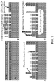
- FIG. 7 shows an exemplary process of fabricating a thin-film-based piezoelectric fan.
- the process may start with a Si substrate and then deposit a stack of layers, such as a SiO 2 -Pt-PZT-Pt stack.
- the SiO 2 oxide layer may be formed by thermal deposition/growth.
- the PZT layer can be formed by spinning of PZT material.
- photolithograph steps are applied to the PZT stack for etching and patterning various layers. These photolithograph steps include coating a Al 2 O 3 ALD passivation layer as masks for etching and patterning of various layers.
- the etching process forms trenches in the PZT stack for structure release in later steps.
- a metallization step through evaporation is applied to the PZT structure to form electrical contacts.
- a XeF 2 etching is performed on the Si substrate to undercut and release the thin-film piezoelectric fan structure.
- electrical connections are formed to interconnect the electrical contacts, for example, by using Au air-bridges.
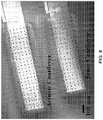
- FIG. 8 shows an SEM image of an exemplary piezoelectric actuate-sense fan pair fabricated using the PZT process described in FIG. 7 .
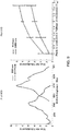
- FIG. 9 shows measured maximum air-velocity at the tip of an exemplary actuate fan by using a RTD sensor close to the tip of the actuate fan. More specifically, the left data plot 900 shows maximum air-velocity as a function of drive frequency on the PZT fan, and the right data plot 910 shows maximum air-velocity as a function of drive voltage at resonance.
- the maximum air-velocity measured at the tip of the piezoelectric fan is ⁇ 7 cm/sec.
- the maximum air-velocity vs. drive voltage data demonstrate the compatibility of such PZT fan for low-voltage platforms.
- FIG. 10 shows the measured DC and AC sense voltages from an exemplary sense fan to provide an integrated feedback for the piezoelectric actuate -sense fan pair.
- the left plot 1000 in FIG. 10 shows that the DC and AC sense voltages are produced due to the reverse piezo-electric effect as a result of lateral air-motion forces.
- the right plot 1010 in FIG. 10 shows a spectrum of AC sense voltage showing AC sense at twice of the drive frequency. The larger random-motion AC signal from the flow indicates a critical flow where the sense fan becomes unstable and starts to flutter, allowing the monitoring of the Reynolds number.
- Table 2 shows exemplary results of fan frequency and displacement analysis for both thin-film PZT fan and bulk PZT fan.
- the analysis for bulk PZT is performed with data measured from laser Doppler vibrometer (LDV) in-plane strobing measurements.
- LDV laser Doppler vibrometer
- the results indicate a very low quality (Q)-factor for the bulk PZT fan structure.
- thin-film PZT fans displays very higher Q-factor that approaches material limited performance. Also, much higher tip-velocity and an integrated fan motion reaching 40 cm/sec have been achieved. In some exemplary thin-film PZT fans, tip velocity > 1 m/sec has been measured.
- FIG. 11 shows exemplary designs for various fans for higher velocity generation, sense-actuate fan pairs and thin-film high voltage transformers. These designs were created to evaluate performance of piezo-fans and sense-actuate fan pairs over a broad range of devices.
- the bottom left devices show sense-actuate fan pairs with a broad range of frequencies, with identical sense fan and actuate fan in each pair.
- the bottom right devices are fans for producing air-flow without any feedback but covering a wide range of frequencies for enhanced flow-rate production for driving ions into the IMS device.
- the top left corner shows implementations of PZT transformers for high-voltage generation using thin-film PZT.
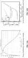
- FIG. 12A shows energy distribution of emitted primary electrons from Ni-63.
- FIG. 12B shows current measurement in an ion-gauge using Ni-63.
- Radioactive Ni-63 by itself may not be ideal for handling, processing or direct use in ionization. Care must be taken to avoid contamination and flaking during handling of hot Ni-63 to avoid long term radioactive contamination of any kind or health damage.
- electro-plating cold Ni on top of hot Ni-63 and using the structure as a component for ionization allows for much safer handling.
- FIG. 13 shows an example of using a cold Ni/hot Ni-63 compound as an ionization module. As can be seen in FIG. 13 , a cold Ni layer is electro-plated on a substrate and then hot Ni-63 can be adhered/glued to the cold Ni layer. A very thin cold Ni film can be coated over the hot Ni-63. The whole module can be clamped down with aluminum clamps.
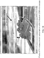
- FIG. 14 shows an optical image of a physical setup for measuring current vs. bias voltage (IV) and for measuring current vs. test electrode distance to the Ni-film (IZ, i.e., current versus gap Z) of a Ni-63 ionizer.
- FIG. 15 shows exemplary results of IZ measurements (left plot 1500) and IV measurements (right plot 1510) of an exemplary Ni-63 ionizer using the physical setup shown in FIG. 14 .
- the currents shown in FIG. 15 are obtained with no bias voltage between the electrode and Ni-film.
- FIG. 16 shows exemplary results of IV measurements (left plot 1600) and IZ measurements (right plot 1610) of an exemplary Ni-63 ionizer using the test setup shown in FIG. 14 .
- the blue curve corresponds to when the electrode is flush on 0-80 screws and the red curve corresponds to when the electrode is at stage limit.
- the results show more stable current partially because, compared to the measurements setup to obtain the results in FIG. 15 , the copper electrode is better aligned to obtain the results in FIG. 16 .
- FIG. 17 shows optical images of an exemplary setup for measuring ionization current with a bias applied across electrodes and a fan for blowing ionized air.
- a rotary fan 1702 is used in the test setup to blow ionized air towards electrodes, which are varied at different distances from the Ni film.
- the left image 1700 in FIG. 17 shows when the fan 1702 is turned off and the right image 1710 shows when the fan 1702 is turned on.
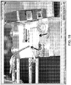
- FIG. 18 shows another image at a different angle of the same setup shown in FIG. 17 for measuring ionization current with a bias applied across electrodes. No significant difference was observed in measured ionization current when the fan 1702 is turned on and when it is turned off.
- a Lithium Niobate (LiNbO 3 ) pyroelectric ionization technique uses Z-cut LiNbO 3 crystal with an attached resistive heater attached to the crystal.
- the heater can be implemented using a 68 ohm, 0.5-W resistor, epoxied to the LiNbO 3 with a commercial thermal adhesive on +z plate of the LiNbO 3 crystal.
- the Z-plate of the crystal is exposed to the ambient air for ionization.
- the resistor is heated with Joule heating to cause crystal temperature to increase.
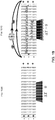
- FIG. 19 shows conceptual diagrams of a Z-cut LiNbO 3 crystal with (right plot 1910) and without (left plot 1900) heating.
- ⁇ T > 0 When the crystal is heated (i.e., ⁇ T > 0), positive and negative charges redistribute to cause a potential difference across the crystal.
- LiNbO 3 crystal can be a better ionizer candidate than PZT material for ionization because the intrinsic pyroelectric coefficient of a LiNbO 3 crystal is much higher than that can be tailored for pyroelectric PZT (e.g., it's ⁇ 3-5 ⁇ C/m 2 K for PZT materials vs.70-100 ⁇ C/m 2 K for LiNbO 3 ). Moreover, the dielectric constant is much lower in LiNbO 3 crystal at 46 ⁇ 0 compared 1100 ⁇ 0 for PZT. Hence it is typically more convenient to obtain higher voltages with lithium niobate compared to PZT. However, with sufficiently long length of PZT and heating, ionization can also be implemented with PZT materials.
- FIG. 20A shows infrared (IR) camera images of temperature profiles of a resistive heater without an voltage applied across the resistor (left image) and with a 5V voltage applied across the resistor (right image).
- FIG. 20B show an exemplary assembly of a LiNbO 3 ionizer crystal with heater attached to the back of the crystal.
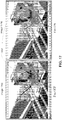
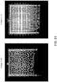
- FIG. 21 shows light patterns of DBD at the surface of a piezo-transformer (PT) 1 minute after the onset of discharge (left image 2100) and after continuous stable discharge (right image 2110).
- FIG. 22 shows a PZT poled along two different axes within the same material.
- the voltage is applied across the thickness of the PZT plate with the segment on the left section 2200 of the plate poled in the thickness direction. This voltage excites the resonant mode of the PZT plate to create a strain wave on the other section 2210 of the plate on the right.
- the poling is realized along the length of the PZT plate.
- poled PZT materials have been used as bulk PZT transformers, such materials have not been used for micro-scale devices and systems.
- FIG. 23 shows simulation results of bimorph piezo-transformer (PT) operation.
- the input or drive electrodes of the bimorph PT receives AC actuation signals and the device concentrates driving energy from the AC actuation signals into the output electrode to produce high voltages.
- FIG. 24 shows COMSOL simulation results for sense-voltage produced (single-ended) with 1V AC signal applied to the drive electrodes for 450 um (left plot 2400) and 900 um (right plot 2410) wide PT beams. An isotropic loss factor of ⁇ 0.01 is assumed for these simulations.
- FIG. 25 shows an optical image of a PZT high voltage transformer comprised of a PZT structure including beams primarily acting as springs and masses.
- the PZT beam is 450 um wide.
- the two drive electrodes 1 and 2 are significantly longer than the two sense electrodes 1 and 2 where high voltages are obtained.
- FIG. 26 shows an image of an exemplary test setup for a transformer, such as the one shown in FIG. 25 .
- the output was lowered due to loading. For example, 0.3V AC output is obtained for 1 V AC input drive.
- a gain in the output is obtained. For example, a gain of 1.4 ⁇ was obtained for a device with electrodes patterned only on side of the PZT beam for applying signal and ground patterned on the other side of the PZT beam.
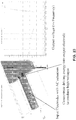
- FIG. 27 shows different sense electrode configurations: a 150 ⁇ 150 square cut out from 450 ⁇ 300 rectangle (plot 2700); a 150 ⁇ 300 cut in a 450 ⁇ 300 horizontal rectangle (plot 2710); and a 150 ⁇ 300 cut in a 450 ⁇ 450 square (plot 2720), all units in um 2 .
- the different design configurations can be used to identify an optimal electrode size because stress generated at the anchor is not uniformly distributed near the anchor. Generally, larger electrodes can cause less charge to develop across the same area causing a lower voltage to be sensed.
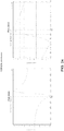
- FIG. 28 shows exemplary simulation results of input voltages (red curves) and output voltages (blue curves) of the bimorph PT for the three configurations shown in FIG. 27 .
- output gains are 0.95, 1.1 and 0.48, respectively for these three configurations.
- the 90 degree phase shift between input and output indicates that the output is the result of resonance, instead of feedthrough.
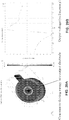
- FIG. 29A shows an exemplary design of a high voltage disk transformer.
- the input electrode is formed over the outer ring of the disk-shaped PZT while the output electrode is formed at the center of the disk-shaped PZT.
- the design allows for concentrating driving energy from the input electrode into the output electrode positioned at the center of the disk structure.
- FIG.29B shows exemplary simulation results of output voltage vs frequency for the design of FIG. 29A .
- FIG. 30 shows an optical image of a fabricated high voltage disk transformer with the proposed input and output electrode configuration.
- FIG. 31 shows exemplary measurement results of corresponding input and output voltage waveforms of the high voltage disk transformer in FIG. 30 with different input and output buffer inclusion options.
- an output gain of ⁇ 16 at resonance can be obtained when both input and output buffers are used in the test setup.
- the control and interface circuits can be implemented using surface mount resistor attached to the LiNbO 3 crystal as heater, powered by a 5V battery.
- the control and interface circuits can be implemented using AD9833 chip-scale waveform generator to provide the AC drive signal, a 5 V battery, and crystal oscillator.
- the control and interface circuits can be substantially the same as those used for the PT ionizer.
- FIG. 32 shows an optical image of an integrated fan and ionizer 3200 based on the same PZT high voltage generator described above.
- the proposed PZT high voltage generator as an ionizer includes a bimorph piezoelectric beam which can be driven by the same principle as the proposed piezoelectric micro-fan. As described previously, the region of ionization of this integrated fan and ionizer 3200 is located at the output electrodes.
- the cantilever shaped piezoelectric beam in this structure can be driven at the resonance of the beam by a drive signal applied to the input electrodes to cause motion at the tip of the beam, thereby generating an air-flow at the tip.
- the ionizer based on LiNBO 3 crystal and a pre-concentrator need heating to function and are successive stages in the proposed gas sensing system, to reduce power consumption.
- some implementations combine the LiNbO 3 crystal ionizer and the pre-concentrator. More specifically, the pre-concentrator material requires heat to desorb the gases that have been adsorbed in the material. This heat, typically generated using a resistor can drain the battery of a portable device.
- the LiNbO 3 crystal requires heat to build the electric field and requires battery energy. By combining the pre-concentrator with the LiNBO 3 crystal, one uses the same heat to desorb the gas and to generate the ionization field, thereby reducing the overall power usage per gas sensing cycle.
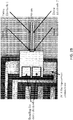
- FIG. 33A shows an exemplary integrated ionizer and pre-concentrator for breath sample detection without tuning on surface mount resistive heater.
- the integrated ionizer and pre-concentrator includes a LiNbO 3 crystal, a layer of pre-concentrator material coated on the top surface of the LiNbO 3 crystal, and a surface mount resistive heater attached to the bottom surface of the LiNbO 3 crystal.
- a surface mount resistive heater attached to the bottom surface of the LiNbO 3 crystal.
- analytes are accumulated on the pre-concentrator material which is attached on top of the LiNbO 3 crystal. Charges in the LiNbO 3 crystal due to poling are neutralized due to surface charges. Note that without heating, the breath analyses attached to the pre-concentrator material are not ionized.
- FIG. 33A shows an exemplary integrated ionizer and pre-concentrator for breath sample detection without tuning on surface mount resistive heater.
- the integrated ionizer and pre-concentrator includes a LiNbO 3 crystal,
- FIG. 33B shows the same integrated ionizer and pre-concentrator in FIG. 33A with the resistive heater turned on after completing sample collection over breath cycles.
- the breath analyses are ionized and released from the pre-concentrator material, which can then flow into IMS ion-channel under the air-flow caused by the piezoelectric fan.
- FIG. 34 presents a table including power consumptions for different modules within the chip-based gas sensor.
- the proposed piezoelectric fan and various proposed ionizers all require very little power and can be operated with 5V or less voltages.
- Pre-concentrator consumes relatively large power which can be the bottom neck for low power requirement.
- One solution is to use the above-described integrated ionizer and pre-concentrator to replace the standalone pre-concentrator.
- Adsorption of volatile organic compounds (VOCs) on functionalized surfaces can be used to modulate or tune the physical and chemical properties of the functionalized surfaces.
- Graphene is a 2-D material with extraordinary electrical and mechanical properties. Graphene can adsorb molecules reversibly on its surface leading to electron-transfer between adsorbate and graphene, causing graphene conductance modulation. Furthermore, graphene can be patterned on micromachined suspended membranes to sense the mass of the adsorbed molecules which has been used for thin-film spun-on polymer thermogravimetry analysis.
- FIG. 35A shows graphene patterned on micromachined suspended membranes. More specifically, FIG. 35A shows pristine graphene-on-nitride. Graphene, when deposited on silicon nitride leaves vacant orbitals with electrons available for conduction. As can be seen in FIG. 35A , the out-of-plane p-orbitals contain electrons for conduction.
- the described properties of graphene can be used to sense dynamic adsorption of various compounds on graphene. In the presence of these compounds, the graphene conductance reaches a steady-state which is different from the conductance prior to the adsorption.
- the molecules can eventually be desorbed by raising the temperature of graphene by the self Joule-heating of the graphene resistor, thus paving the way for a reusable gas sensing technique.
- FIG. 35B shows using graphene patterned micromachined suspended membranes as an electrical sensor to sense the mass of the adsorbed molecules without heating the structure.
- polymer-graphene interactions modulate electrical conduction.
- the partial bonds and interactions between the polymer molecules and graphene affect the availability of conduction electrons, hence changing graphene resistance.
- FIG. 35C shows using graphene patterned micromachined suspended membranes as an mechanical sensor to sense the mass of the adsorbed molecules while heating the structure with a resistive heater.
- polymer vaporization by resistive heating is sensed based on a resonance-frequency shift. More specifically, when the graphene resistance is used for heating the polymer, the resonance frequency of the membrane changes when the polymer evaporates, thereby enabling mass-sensing.
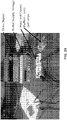
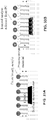
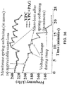
- FIG. 36 shows exemplary results of mass sensing for different adsorbed materials on the graphene surface. As shown in FIG. 36 , mass sensing measurement for the gas can be measured over-time and cycled thermally with input power to the graphene heater.
- FIG. 37 shows exemplary results of electrical sensing for different adsorbed materials on the graphene surface.
- Adsorption of volatile organic compounds (VOCs) on functionalized surfaces can be used to modulate or tune the physical and chemical properties of the functionalized surfaces.
- Graphene is a 2-D material with extraordinary electrical and mechanical properties. Graphene can adsorb molecules reversibly on its surface leading to electron-transfer between adsorbate and graphene, causing graphene conductance modulation. Furthermore, graphene can be patterned on micromachined suspended membranes to sense the mass of the adsorbed molecules which has been used for thin-film spun-on polymer thermogravimetry analysis.
- FIG. 35A shows graphene patterned on micromachined suspended membranes. More specifically, FIG. 35A shows pristine graphene-on-nitride. Graphene, when deposited on silicon nitride leaves vacant orbitals with electrons available for conduction. As can be seen in FIG. 35A , the out-of-plane p-orbitals contain electrons for conduction.
- the described properties of graphene can be used to sense dynamic adsorption of various compounds on graphene. In the presence of these compounds, the graphene conductance reaches a steady-state which is different from the conductance prior to the adsorption.
- the molecules can eventually be desorbed by raising the temperature of graphene by the self Joule-heating of the graphene resistor, thus paving the way for a reusable gas sensing technique.
- FIG. 35B shows using graphene patterned micromachined suspended membranes as an electrical sensor to sense the mass of the adsorbed molecules without heating the structure.
- polymer-graphene interactions modulate electrical conduction.
- the partial bonds and interactions between the polymer molecules and graphene affect the availability of conduction electrons, hence changing graphene resistance.
- FIG. 35C shows using graphene patterned micromachined suspended membranes as an mechanical sensor to sense the mass of the adsorbed molecules while heating the structure with a resistive heater.
- polymer vaporization by resistive heating is sensed based on a resonance-frequency shift. More specifically, when the graphene resistance is used for heating the polymer, the resonance frequency of the membrane changes when the polymer evaporates, thereby enabling mass-sensing.
- FIG. 36 shows exemplary results of mass sensing for different adsorbed materials on the graphene surface. As shown in FIG. 36 , mass sensing measurement for the gas can be measured over-time and cycled thermally with input power to the graphene heater.
- FIG. 37 shows exemplary results of electrical sensing for different adsorbed materials on the graphene surface.
Landscapes
- Chemical & Material Sciences (AREA)
- Physics & Mathematics (AREA)
- Health & Medical Sciences (AREA)
- Life Sciences & Earth Sciences (AREA)
- Biochemistry (AREA)
- Electrochemistry (AREA)
- Chemical Kinetics & Catalysis (AREA)
- Analytical Chemistry (AREA)
- General Health & Medical Sciences (AREA)
- General Physics & Mathematics (AREA)
- Immunology (AREA)
- Pathology (AREA)
- Spectroscopy & Molecular Physics (AREA)
- Toxicology (AREA)
- Molecular Biology (AREA)
- Other Investigation Or Analysis Of Materials By Electrical Means (AREA)
- Sampling And Sample Adjustment (AREA)
Description
- This patent document claims priority and the benefits of
U.S. Provisional Application No. 61/932,234 - This patent document relates to systems, devices, and processes that use molecular sensor technologies including a chip scale gas sensor capable of integration with mobile communication devices, such as PDA or smart phone devices.
- A biological sensor or biosensor is an analytical tool that can detect a chemical, substance or organism using a biologically sensitive component coupled with a transducing element to convert a detection event into a signal for processing and/or display. Biosensors can use biological materials as the biologically sensitive component, e.g., such as biomolecules including enzymes, antibodies, aptamers, peptides, nucleic acids, etc., or small molecules such as carbohydrates, as well as virus and living cells. For example, molecular biosensors can be configured to use specific chemical properties or molecular recognition mechanisms to identify target agents. Biosensors can use the transducer element to transform a signal resulting from the detection of an analyte by the biologically sensitive component into a different signal that can be addressed by a suitable transduction mechanism, for example, electrical, magnetic, mechanical, physicochemical, electrochemical, optical, piezoelectric, or others.
- Molecular sensor devices, systems, and techniques are disclosed for measuring ion-mobility to detect gases in ultra-portable packages capable of integration with mobile communication devices, such as PDA or smart phone devices. The power supply for the disclosed gas sensors can be the standard cell-phone battery. The disclosed sensors can include a piezoelectric micro fan that is low power, low voltage, and sufficiently small to provide air molecule samples at rates determined by convection. In other embodiments, the disclosed sensor devices include a chip-size ionizer for gas analyte ionization.
- In one aspect, a gas sensor device is disclosed. This gas sensor device includes: a pre-concentration module to collect and concentrate a gas-phase chemical for analysis; a piezoelectric fan including a pair of drive and sense fans, the drive fan being configured to produce an air-flow through acoustic streaming to drive the gas-phase chemical released by the pre-concentration module to one or more downstream modules, the sense fan being configured to sense a lateral turbulent air-motion to provide a feedback signal for controlling the drive fan; an ionizer downstream from the piezoelectric fan to ionize the gas-phase chemical; and a gas sensor downstream from the piezoelectric fan and the ionizer to detect the ionized gas-phase chemical driven by the piezoelectric fan. The piezoelectric fan can include a stack of thin-film layers that includes a thin-film piezoelectric layer. The ion-gas sensor device is made into an ultra-portable package capable of integration with mobile communication devices, such as PDA devices or smart phones.
-
-
FIG. 1 shows a block diagram of an exemplary chip scale gas sensor of the disclosed technology. -
FIG. 2 shows a diagram of an exemplary chip scale ion-gas sensor of the disclosed technology that includes a piezoelectric sense-drive fan pair, a radioactive Ni-63 film for gas ionization, and an ion-mobility spectrometry (IMS) array gas sensor integrated as a package. -
FIG. 3A shows exemplary dimensions of an exemplary micro pre-concentrator. -
FIG. 3B shows exemplary dimensions of an exemplary piezoelectric fan. -
FIG. 3C shows exemplary dimensions of an exemplary Ni-63 ionizer and an exemplary LiNbO3 ionizer. -
FIG. 3D shows exemplary dimensions of an exemplary IMS gas sensor. -
FIG. 4 shows a schematic of an exemplary bio-sniffing chip that includes various modules of an exemplary chip-scale gas sensor. -
FIG. 5 shows exemplary streaming air-flow and re-circulating vortices above the tip of a piezoelectric fan and equations for air velocity and force as functions of devices parameters and constants. -
FIG. 6 shows an exemplary gas sensing device including a piezoelectric drive-sense fan pair for generating an air-flow within the gas sensing device. -
FIG. 7 shows an exemplary process of fabricating a thin-film-based piezoelectric fan. -
FIG. 8 shows an SEM image of an exemplary piezoelectric actuate-sense fan pair fabricated using the PZT process described inFIG. 7 . -
FIG. 9 shows measured maximum air-velocity at the tip of an exemplary actuate fan by using a resistance temperature detector sensor close to the tip of the actuate fan. -
FIG. 10 shows the measured DC and AC sense voltages from an exemplary sense fan to provide an integrated feedback for the piezoelectric sense-actuate fan pair. -
FIG. 11 shows exemplary tape-out designs for various fans for higher velocity generation, sense-actuate fan pairs and thin-film high voltage transformers. -
FIG. 12A shows energy distribution of emitted primary electrons from radioactive Ni-63 (hot Ni-63). -
FIG. 12B shows current measurement in an ion-gauge using radioactive Ni-63. -
FIG. 13 shows an example of using a cold Ni/hot Ni-63 compound as an ionization module. -
FIG. 14 shows an optical image of a physical setup for measuring current vs. bias voltage (IV) and for measuring current vs. test electrode distance to the Ni-film (IZ, i.e., current versus gap Z) of a Ni-63 ionizer. -
FIG. 15 shows exemplary results of IZ measurements (left plot) and IV measurements (right plot) of an exemplary Ni-63 ionizer using the physical setup shown inFIG. 14 . -
FIG. 16 shows exemplary results of IV measurements (left plot) and IZ measurements (right plot) of an exemplary Ni-63 ionizer using the test setup shown inFIG. 14 . -
FIG. 17 shows optical images of an exemplary setup for measuring ionization current with a bias applied across electrodes and a fan for blowing ionized air. -
FIG. 18 shows another image at a different angle of the same test setup shown inFIG. 17 for measuring ionization current with a bias applied across electrodes. -
FIG. 19 shows conceptual diagrams of a Z-cut LiNbO3 crystal with (right plot) and without (left plot) heating. -
FIG. 20A shows infrared (IR) camera images of temperature profiles of a resistive heater without an voltage applied across the resistor (left image) and with a 5V voltage applied across the resistor (right image). -
FIG. 20B show an exemplary assembly of a LiNbO3 ionizer crystal with heater attached to the back of the crystal. -
FIG. 21 shows light patterns of dielectric barrier discharge (DBD) at the surface of a piezo-transformer (PT) 1 minute after the onset of discharge (left image) and after continuous stable discharge (right image). -
FIG. 22 shows a PZT poled along two different axes within the same material. -
FIG. 23 shows simulation results of bimorph piezo-transformer (PT) operation. -
FIG. 24 shows COMSOL simulation results for sense-voltage produced (single-ended) with 1V AC signal applied to the drive electrodes for 450 um (left plot) and 900 um (right plot) wide PT beams. An isotropic loss factor of ∼0.01 is assumed for these simulations. -
FIG. 25 shows an optical image of a PZT high voltage transformer comprised of a PZT structure including beams primarily acting as springs and masses. -
FIG. 26 shows an image of an exemplary test setup for a PZT transformer, such as the one shown inFIG. 25 . -
FIG. 27 shows different sense electrode configurations: a 150×150 square cut out from 450×300 rectangle (plot 1); a 150×300 cut in a 450×300 horizontal rectangle (plot 2); and a 150×300 cut in a 450×450 square (plot 3), all units in um2. -
FIG. 28 shows exemplary simulation results of input voltages (red curves) and output voltages (blue curves) of the bimorph PT for the three configurations shown inFIG. 27 . -
FIG. 29A shows an exemplary design of a high voltage disk transformer. -
FIG.29B shows exemplary simulation results of output voltage vs. frequency for the design ofFIG. 29A . -
FIG. 30 shows an optical image of a fabricated high voltage disk transformer with the proposed input and output electrode configuration. -
FIG. 31 shows exemplary measurement results of corresponding input and output voltage waveforms of the high voltage disk transformer inFIG. 30 with different input and output buffer inclusion options. -
FIG. 32 shows an optical image of an integrated fan and ionizer based on the PZT high voltage generator. -
FIG. 33A shows an exemplary integrated ionizer and pre-concentrator for breath sample detection without tuning on surface mount resistive heater. -
FIG. 33B shows the same integrated ionizer and pre-concentrator inFIG. 33A with the resistive heater turned on after completing sample collection over breath cycles. -
FIG. 34 presents a table including power consumptions for different modules within the chip-based gas sensor. -
FIG. 35A shows graphene patterned on micromachined suspended membranes. -
FIG. 35B shows using graphene patterned micromachined suspended membranes as an electrical sensor to sense the mass of the adsorbed molecules without heating the structure. -
FIG. 35C shows using graphene patterned micromachined suspended membranes as an mechanical sensor to sense the mass of the adsorbed molecules while heating the structure with a resistive heater. -
FIG. 36 shows exemplary results of mass sensing for different adsorbed materials on the graphene surface. -
FIG. 37 shows exemplary results of electrical sensing for different adsorbed materials on the graphene surface. - Table 1 shows comparing piezoelectric fan designs with conventional fan designs.
- Table 2 shows fan performance analysis (comparing thin film PZT fan with bulk PZT fan).
- Molecular sensor devices, systems, and techniques are disclosed for measuring ion-mobility to detect gases in ultra-portable packages capable of integration with mobile communication devices, such as PDA devices or smart phones. The power supply for the disclosed gas sensors can be the standard cell-phone battery. The disclosed sensors can include a piezoelectric micro fan that is low power, low voltage, and sufficiently small to provide air molecule samples at rates determined by convection. In other embodiments, the disclosed sensor devices include a chip-size ionizer for gas analyte ionization.
- In some implementations, the disclosed molecular sensor devices include a chip-scale gas sensor using a low-voltage thin-film piezoelectric sense-actuate fan pair.
- In one embodiment, an iongas sensor device is disclosed. This ion-gas sensor device includes: a pre-concentration module to collect and concentrate a gas-phase chemical for analysis; a piezoelectric fan to produce an air-flow through acoustic streaming to drive the gas-phase chemical released by the pre-concentration module to one or more downstream modules; an ionizer downstream from the piezoelectric fan to ionize the gas-phase chemical; and a gas sensor downstream from the piezoelectric fan and the ionizer to detect the ionized gas-phase chemical driven by the piezoelectric fan. The piezoelectric fan can include a stack of thin-film layers that includes a thin-film piezoelectric layer. The ion-gas sensor device is made into an ultra-portable package capable of integration with mobile communication devices, such as PDA devices or smart phones.
- Microscale ion-mobility measurement is an approach to sensing gases in ultra-portable packages such as the burgeoning hand-held smart-phone markets. A key component of a gas sensor is the ability to sample the air molecules at rates determined by convection rather than diffusion for faster detection time. Embodiments of the disclosed technology include devices having a piezoelectric micro-fan, including a micro-fan architecture that is low power (e.g., 10.6 mW/sccm), low voltage (e.g., 8.5 V/sccm), and sufficiently small (0.1mm3/sccm). Embodiments of the disclosed technology includes also include various chip-size ionizers for gas analyte ionization. In some implementations, for example, the devices can include a multi-electrode configuration of ion-detection with less than 5V operating voltage. Exemplary implementations of the disclosed technology described herein demonstrate a pathway towards a chip-scale ion-mobility based gas detector with a process compatible with the ion-detection system, and the actuate and sense micro-fan architecture presented here.
-
FIG. 1 shows a block diagram of an exemplary chipscale gas sensor 100 of the disclosed technology. This chip scale gas sensor includes, in the order of the input side to the output side, a pre-concentrator 102, apiezoelectric fan 104 for air pumping, anionizer 106 for gas ionization, an ion-mobility spectrometry (IMS)gas sensor 108, and adata analyzer 110. In some embodiments,data analyzer 110 is not part of the chipscale gas sensor 100 and the chip scale gas sensor uses a processor of a mobile device for processing the data generated byIMS gas sensor 108. In some embodiments, the pre-concentrator 102 and theionizer 106 are integrated In other embodiments, thepiezoelectric fan 104 and theionizer 106 are integrated as a combined module. Furthermore, other orders of the modules shown inFIG. 1 and options for integrating these modules are possible. The basic functionalities of the illustrated modules of the chipscale gas sensor 100 are now described. - The pre-concentrator module performs the task of collecting volatile organic compounds (VOCs) or other gas analytes and concentrating these compounds before they are analyzed. For example, when the chip scale gas sensor is used as a breath sensor, the pre-concentrator collects VOCs during a regular phone call/electronic device usage over 2-3 minutes from the user's breath when the user talks. The module typically accumulates these compounds on a film layer that is functionalized for molecule collection and concentration. For analysis, the pre-concentrator is typically heated to release these molecules from the functionalized film. The heating system is typically considered a part of the pre-concentrator.
- The piezoelectric fan or simply "piezo fan" is a module that transfers the collected gas compounds that are released by the heated pre-concentrator and transfers them using acoustic streaming (like a blowing fan) to the ionizer for ionization. The air-flow created by the piezo fan also drives the ionized gas analytes toward the IMS gas sensor. Various embodiments of the disclosed technology provide both a thin-film-based piezoelectric fan made by microfabrication and a bulk piezoelectric fan made by micro-machining.
- The ionizer is a module that performs the task of ionizing the gas compounds blown by the fan, i.e., gaining or accepting electrons or ionic charges, prior to analysis by the IMS sensor. Various embodiments of the disclosed technology provide different ionizer designs which have chip-scale integration capabilities. For example, one disclosed ionizer design uses radioactive Ni-63 (also referred to as "hot nickel" or "hot Ni-63" hereinafter) which is natural electron-emitter and has stability in ionization up to 100 years corresponding to its lifetime. Another ionizer design is based on pyroelectricity (i.e., heating to produce large electric potential difference) of lithium niobate (LiNbO3) that enables ionization of the compounds when the LiNbO3 crystal is cycled to rapidly increase or decrease in temperature. Yet another ionizer design uses a bulk piezoelectric beam with electrodes patterned on the beam to produce large strain at the beam anchor to enable large electric fields across small gaps, which in turn produces ions.
- IMS sensor is a module that detects the ionized compounds that are flown by the piezoelectric fan and uses the charge to mass ratio (i.e., ion mobility) of the compounds for identifying the compounds. Data analyzer is a computing module, implemented in software or hardware or both, for interpreting and analyzing the data that is collected from the IMS sensor.
-
FIG. 2 shows a diagram of an exemplary chip scale ion-gas sensor of the disclosed technology that includes a piezoelectric sense-drive fan pair, a radioactive Ni-63 film for gas ionization, and an IMS array gas sensor integrated as a package. The modules depicted inFIG. 2 are described in more detail below. - For chip-size gas sensor integration, each module described above should have a chip size, as shown in
FIG. 3A-FIG. 3D. FIG. 3A shows exemplary dimensions of an exemplary micro pre-concentrator. In this example, the overall dimensions of the micro pre-concentrator are 2.54 cm × 2.54 cm × 1mm in which the active material dimensions are 5 mm × 5 mm × 350 µm.FIG. 3B shows exemplary dimensions of an exemplary piezoelectric fan. In this example, the overall dimensions of the piezo fan are 1 cm × 1 cm × 1.5 mm in which the active material dimensions are 1 mm × 0.8 mm × 0.5 µm. In another example, a more compact piezo fan has total dimensions of 5 mm x 5 mm x 500 µm. In other embodiments, the piezo fans used in the disclosed chip-size gas sensors have even smaller dimensions than the ones described above.FIG. 3C shows exemplary dimensions of an exemplary Ni-63 ionizer and an exemplary LiNbO3 ionizer. In these examples, the overall dimensions of the Ni-63 and LiNbO3 packages are 1.6 cm x 1.6 cm x 5 mm and 5mm x 5 mm x 5 mm, respectively, in which the active dimensions are 1 cm × 1 cm x 100 um and 1 mm x 1 mm x 5 mm, respectively. In another example, a more compact ionizer has total dimensions of 5 mm x 5 mm x 2.5 mm. In other embodiments, the ionizers used in the disclosed chip-size gas sensors have even smaller dimensions than the ones described above.FIG. 3D shows exemplary dimensions of an exemplary IMS gas sensor. In this example, the overall dimensions of the gas sensor are 43.5mm ×26.5mm × 1mm in which the separation and detection region dimensions are 20mm × 3mm × 30µm. Based on the above exemplary dimensions of individual modules, an exemplary total package size of an exemplary chip-based gas sensor is ∼ 3.5 cm x 4.5 cm x 5 mm, which is feasible for a PDA-based or smart phone-based portable gas-sensor. However, much smaller total package sizes of chip-based gas sensors can be implemented to be more compatible with PDAs and smart phones. -
FIG. 4 shows a schematic of an exemplarybio-sniffing chip 400 that includes various modules of an exemplary chip-scale gas sensor. As can be seen fromFIG. 4 ,bio-sniffing chip 400 includes aninlet 402 for receiving gas samples such as volatile organic compounds (VOCs) from a user's breath, which is located at one end of thebio-sniffing chip 400.Bio-sniffing chip 400 includes a bulk PZT fan 404 located immediately next to theinlet 402, and operating in the KHz range. However, bulk PZT fan 404 can be replaced with a thin-film PZT fan.Bio-sniffing chip 400 includes an integrated ionizer and pre-concentrator 406 located downstream from bulk PZT fan 404. More specifically, integrated ionizer and pre-concentrator 406 includes a LiNbO3 ionizer comprising a LiNbO3 crystal and a surface mount resistive heater, and a pre-concentration functionalized layer attached to the surface of the LiNbO3 ionizer. The integration of the ionizer and the pre-concentrator has the benefit of significantly reducing power consumption of the overall chip-based gas sensor. However, other test chip configurations can use separate ionizer and pre-concentrator, and other types of ionizers.Bio-sniffing chip 400 also includes stacked or single layer electrode forion sensing 408 which is located at the other end ofbio-sniffing chip 400. In other gas-sensing chip configurations, the order of ionizer and fan can be switched. Using different configurations of the gas-sensing chips can facilitate identifying optimal ion-flow in order to avoid cold spots. - In some embodiments of the disclosed technology, a thin-film piezoelectric-SiO2 composite unimorph actuated at resonance is used as a fan (also referred to as a thin-film piezoelectric fan) to induce flow of the ions into a MDS-IMS device convectively by shedding vortices near the fan-tip. The micro-fan peak-to-peak displacement, magnified at resonance, produces air flow along its axis by shedding air vortices close to its tip, as well as re-circulating loops above surface of the fan. Devices based on thin-film piezoelectric fan are compatible with low-voltage (e.g., < 5V) and low power platforms. Flow-rates of up to 7 cm/s have been measured with these devices. Another piezoelectric fan is placed close to the drive fan to sense turbulent air-motion, and to provide a feedback signal for controlling the drive fan. The piezoelectric drive fan and the piezoelectric sense fan thus form a "piezoelectric drive-sense fan pair."
-
FIG. 5 shows exemplary streaming air-flow and re-circulating vortices above the tip of a piezoelectric fan and equations for air velocity and force as functions of devices parameters and constants. The flow due to the piezoelectric fan is a function of Reynolds number of the resulting flow. The Reynolds number is a function of the tip-substrate gap, and etch-holes on the surface of the fan. The channel can be designed to achieve a desired flow that can be used in micro channels compatible with small form factors presented in hand-held electronic information devices. InFIG. 5 , Fstream is the streaming force for driving ions into the IMS device, and νstream is the velocity of ions being streamed. - Multilayer analysis for arbitrary piezoelectric-elastic layer stacks, and exemplary measured data from DC actuation from 0-6V, yielded piezoelectric coupling coefficient d31 = -85.8±5 pC/N for the PZT films, less than the values for bulk PZT but within expectation for multi-layer stressed thin-film devices. Resonance frequencies were measured to be at 614 Hz and 505 Hz, with peak-to-peak tip-displacement > 200 um 2-Vpp, with 2.5 mW power input. A RTD element was used to measure air-velocity close to the tip of the fan.
- Table 1 compares piezoelectric fan designs with conventional fan designs.
Table 1: Comparing piezoelectric fan designs with conventional fan designs Work Max Flow (µL/min) Nominal Voltage Power (mW) Conventional Micropump 4000 100V ∼57 Conventional Electrostatic Micro fan 10 100Vp-p - Exemplary Piezofan of Disclosed Tech 235.6 2Vp-p 2.5 -
FIG. 6 shows an exemplary gas sensing device including a piezoelectric drive-sense fan pair 600 for generating an air-flow within the gas sensing device. In the proposed gas sensing device, piezoelectric drive-sense fan pair 600 for air-flow generation, and the radioactive Ni-63film 602 for gas ionization are preceded by the pre-concentrator (not shown). - As can be seen in
FIG. 6 , the drive fan or the "actuate fan" of drive-sense fan pair 600 actuated at resonance produces a large amplitude tip vibration to enable mechanical power-transfer to drive an analyte mixture from the pre-concentrator toward an IMS device. The sense fan of drive-sense fan pair 600 next to the drive fan measures a lateral turbulent air-motion to provide feedback signal for controlling the drive signal (e.g., V cos(ωt)) of the drive fan XXX.FIG. 6 also shows radioactive Ni-63film 602 placed directly under the vibrating tip of the actuate fan. Ni-63film 602 includes high-energy density radioactive electron-emitting Ni-63 which is capable of causing broadband ionization of the analytes. In some embodiments, Ni-63film 602 emits primary and secondary electrons to produce ∼nA of ionization current. By combining the fan module and the ionization module, the disclosed biosensing device can potentially reduce bio-sensing time from ∼100 seconds to < 0.1 second compared to the diffusion-limited sensing techniques. -
FIG. 7 shows an exemplary process of fabricating a thin-film-based piezoelectric fan. As shown insubplot 1 ofFIG. 7 , the process may start with a Si substrate and then deposit a stack of layers, such as a SiO2-Pt-PZT-Pt stack. The SiO2 oxide layer may be formed by thermal deposition/growth. The PZT layer can be formed by spinning of PZT material. Next, as shown insubplot 2 ofFIG. 7 , photolithograph steps are applied to the PZT stack for etching and patterning various layers. These photolithograph steps include coating a Al2O3 ALD passivation layer as masks for etching and patterning of various layers. As shown insubplot 2, the etching process forms trenches in the PZT stack for structure release in later steps. Next, as shown insubplot 3 ofFIG. 7 , a metallization step through evaporation is applied to the PZT structure to form electrical contacts. Next, as shown insubplot 4 ofFIG. 7 , a XeF2 etching is performed on the Si substrate to undercut and release the thin-film piezoelectric fan structure. Also, electrical connections are formed to interconnect the electrical contacts, for example, by using Au air-bridges. -
FIG. 8 shows an SEM image of an exemplary piezoelectric actuate-sense fan pair fabricated using the PZT process described inFIG. 7 . - Exemplary implementations of the exemplary devices were performed. The exemplary piezoelectric actuate-sense fan pairs with widths of 200 µm and
lengths 800 µm and 1000 µm, respectively, were tested in micro-channels.FIG. 9 shows measured maximum air-velocity at the tip of an exemplary actuate fan by using a RTD sensor close to the tip of the actuate fan. More specifically, theleft data plot 900 shows maximum air-velocity as a function of drive frequency on the PZT fan, and theright data plot 910 shows maximum air-velocity as a function of drive voltage at resonance. The maximum air-velocity measured at the tip of the piezoelectric fan is ∼7 cm/sec. The maximum air-velocity vs. drive voltage data demonstrate the compatibility of such PZT fan for low-voltage platforms. -
FIG. 10 shows the measured DC and AC sense voltages from an exemplary sense fan to provide an integrated feedback for the piezoelectric actuate -sense fan pair. For example, theleft plot 1000 inFIG. 10 shows that the DC and AC sense voltages are produced due to the reverse piezo-electric effect as a result of lateral air-motion forces. The right plot 1010 inFIG. 10 shows a spectrum of AC sense voltage showing AC sense at twice of the drive frequency. The larger random-motion AC signal from the flow indicates a critical flow where the sense fan becomes unstable and starts to flutter, allowing the monitoring of the Reynolds number. - Table 2 shows exemplary results of fan frequency and displacement analysis for both thin-film PZT fan and bulk PZT fan. The analysis for bulk PZT is performed with data measured from laser Doppler vibrometer (LDV) in-plane strobing measurements. The results indicate a very low quality (Q)-factor for the bulk PZT fan structure. In contrast, thin-film PZT fans displays very higher Q-factor that approaches material limited performance. Also, much higher tip-velocity and an integrated fan motion reaching 40 cm/sec have been achieved. In some exemplary thin-film PZT fans, tip velocity > 1 m/sec has been measured.

-
FIG. 11 shows exemplary designs for various fans for higher velocity generation, sense-actuate fan pairs and thin-film high voltage transformers. These designs were created to evaluate performance of piezo-fans and sense-actuate fan pairs over a broad range of devices. The bottom left devices show sense-actuate fan pairs with a broad range of frequencies, with identical sense fan and actuate fan in each pair. The bottom right devices are fans for producing air-flow without any feedback but covering a wide range of frequencies for enhanced flow-rate production for driving ions into the IMS device. The top left corner shows implementations of PZT transformers for high-voltage generation using thin-film PZT. - Ni-63 is an electron-emitting radioactive material with a high-energy density, yet benign in terms of penetrating power. Ni-63 can also be electro-plated in thin films. The half-life of Ni-63 is 100 years and it is capable of producing primary electrons of energies 0-70 keV with average energy = 17 keV. A 1 mm × 1 mm Ni-63 film has an activity of ∼100 µCurie or 3.7 x 10⁶ disintegrations per second with average energy of 17 keV and low cross-section of ionization. When accelerated across a potential difference, the primary electrons strike metal electrodes producing secondary electrons with energies ∼ 0-300 eV, which is sufficient to overcome the first ionization energies of most compounds.
FIG. 12A shows energy distribution of emitted primary electrons from Ni-63.FIG. 12B shows current measurement in an ion-gauge using Ni-63. - Radioactive Ni-63 by itself may not be ideal for handling, processing or direct use in ionization. Care must be taken to avoid contamination and flaking during handling of hot Ni-63 to avoid long term radioactive contamination of any kind or health damage. However, electro-plating cold Ni on top of hot Ni-63 and using the structure as a component for ionization allows for much safer handling.
FIG. 13 shows an example of using a cold Ni/hot Ni-63 compound as an ionization module. As can be seen inFIG. 13 , a cold Ni layer is electro-plated on a substrate and then hot Ni-63 can be adhered/glued to the cold Ni layer. A very thin cold Ni film can be coated over the hot Ni-63. The whole module can be clamped down with aluminum clamps. -
FIG. 14 shows an optical image of a physical setup for measuring current vs. bias voltage (IV) and for measuring current vs. test electrode distance to the Ni-film (IZ, i.e., current versus gap Z) of a Ni-63 ionizer.FIG. 15 shows exemplary results of IZ measurements (left plot 1500) and IV measurements (right plot 1510) of an exemplary Ni-63 ionizer using the physical setup shown inFIG. 14 . The currents shown inFIG. 15 are obtained with no bias voltage between the electrode and Ni-film. As can be seen in IZ measurement ofFIG. 15 , 110 pA of current is measured when the electrode is flush on 0-80 screws, and 70-80 pA of current is measured when the electrode is at stage limit (i.e., the maximum distance from Ni film). The results show large variation in current which can be due to film-electrode misalignment and copper electrode is not exactly flush on the stage. -
FIG. 16 shows exemplary results of IV measurements (left plot 1600) and IZ measurements (right plot 1610) of an exemplary Ni-63 ionizer using the test setup shown inFIG. 14 . In the IV measurement, the blue curve corresponds to when the electrode is flush on 0-80 screws and the red curve corresponds to when the electrode is at stage limit. The results show more stable current partially because, compared to the measurements setup to obtain the results inFIG. 15 , the copper electrode is better aligned to obtain the results inFIG. 16 . -
FIG. 17 shows optical images of an exemplary setup for measuring ionization current with a bias applied across electrodes and a fan for blowing ionized air. As can be seen, arotary fan 1702 is used in the test setup to blow ionized air towards electrodes, which are varied at different distances from the Ni film. Theleft image 1700 inFIG. 17 shows when thefan 1702 is turned off and theright image 1710 shows when thefan 1702 is turned on.FIG. 18 shows another image at a different angle of the same setup shown inFIG. 17 for measuring ionization current with a bias applied across electrodes. No significant difference was observed in measured ionization current when thefan 1702 is turned on and when it is turned off. This result can be due to that the rotary fan used in these measurements does not produce large flow rates and the bulk electrodes are not optimized for testing. There is also lack of a stage capable of fine control of electrode placement relative to the Ni film. Hence, there is a need to replace the rotary fan with a piezoelectric micro-fan and to replace the bulk electrodes with microfabricated electrodes. - Alternatively to using Ni-63 ionizer, a Lithium Niobate (LiNbO3) pyroelectric ionization technique uses Z-cut LiNbO3 crystal with an attached resistive heater attached to the crystal. For example, the heater can be implemented using a 68 ohm, 0.5-W resistor, epoxied to the LiNbO3 with a commercial thermal adhesive on +z plate of the LiNbO3 crystal. When used in an ionization setup, the Z-plate of the crystal is exposed to the ambient air for ionization. The resistor is heated with Joule heating to cause crystal temperature to increase. Potential difference created in the LiNbO3 crystal can be measured as a function of increase in temperature (ΔT):

-
FIG. 19 shows conceptual diagrams of a Z-cut LiNbO3 crystal with (right plot 1910) and without (left plot 1900) heating. As can be seen in FIG. XX, when Z-cut LiNbO3 crystal is not heated (i.e., ΔT = 0), positive and negative charges in the crystal distribute evenly to neutralize each other. When the crystal is heated (i.e., ΔT > 0), positive and negative charges redistribute to cause a potential difference across the crystal. LiNbO3 crystal can be a better ionizer candidate than PZT material for ionization because the intrinsic pyroelectric coefficient of a LiNbO3 crystal is much higher than that can be tailored for pyroelectric PZT (e.g., it's ∼3-5 µC/m2K for PZT materials vs.70-100 µC/m2K for LiNbO3). Moreover, the dielectric constant is much lower in LiNbO3 crystal at 46ε0 compared 1100ε0 for PZT. Hence it is typically more convenient to obtain higher voltages with lithium niobate compared to PZT. However, with sufficiently long length of PZT and heating, ionization can also be implemented with PZT materials. -
FIG. 20A shows infrared (IR) camera images of temperature profiles of a resistive heater without an voltage applied across the resistor (left image) and with a 5V voltage applied across the resistor (right image).FIG. 20B show an exemplary assembly of a LiNbO3 ionizer crystal with heater attached to the back of the crystal. - It is known that continuous stable emission of ions can be obtained at the surface of a PZT material using dielectric barrier discharge (DBD). While poling PZT along two different axes is not usually suited for planar surface and bulk micromachining, it is compatible with conventional thin-film as well as bulk deposition and etching techniques. It is desirable to create the same discharge using in-plane PZT disk-transformers which perform the task of amplifying the voltage and producing high electric field for ionization across small gaps.
FIG. 21 shows light patterns of DBD at the surface of a piezo-transformer (PT) 1 minute after the onset of discharge (left image 2100) and after continuous stable discharge (right image 2110). - Rosen PZT transformers is well-known type of PT which can be used for computer backlights, portable electronic chargers, among other applications.
FIG. 22 shows a PZT poled along two different axes within the same material. As can be seen inFIG. 22 , the voltage is applied across the thickness of the PZT plate with the segment on theleft section 2200 of the plate poled in the thickness direction. This voltage excites the resonant mode of the PZT plate to create a strain wave on theother section 2210 of the plate on the right. Insection 2210, the poling is realized along the length of the PZT plate. The muchlonger length section 2210 versus thethickness section 2200 of the resonator gives rise to a higher voltage giving by the ratio of the length ofsection 2210 to the thickness of the plate. Although poled PZT materials have been used as bulk PZT transformers, such materials have not been used for micro-scale devices and systems. -
FIG. 23 shows simulation results of bimorph piezo-transformer (PT) operation. As can be seen inFIG. 23 , the input or drive electrodes of the bimorph PT receives AC actuation signals and the device concentrates driving energy from the AC actuation signals into the output electrode to produce high voltages.FIG. 24 shows COMSOL simulation results for sense-voltage produced (single-ended) with 1V AC signal applied to the drive electrodes for 450 um (left plot 2400) and 900 um (right plot 2410) wide PT beams. An isotropic loss factor of ∼0.01 is assumed for these simulations. -
FIG. 25 shows an optical image of a PZT high voltage transformer comprised of a PZT structure including beams primarily acting as springs and masses. In this device, the PZT beam is 450 um wide. As can be seen inFIG. 25 , the twodrive electrodes sense electrodes -
FIG. 26 shows an image of an exemplary test setup for a transformer, such as the one shown inFIG. 25 . It is noticed that without input and output buffers for the device, the output was lowered due to loading. For example, 0.3V AC output is obtained for 1 V AC input drive. When the input and output buffers are used in the device, a gain in the output is obtained. For example, a gain of 1.4× was obtained for a device with electrodes patterned only on side of the PZT beam for applying signal and ground patterned on the other side of the PZT beam. -
FIG. 27 shows different sense electrode configurations: a 150×150 square cut out from 450×300 rectangle (plot 2700); a 150×300 cut in a 450×300 horizontal rectangle (plot 2710); and a 150×300 cut in a 450×450 square (plot 2720), all units in um2. The different design configurations can be used to identify an optimal electrode size because stress generated at the anchor is not uniformly distributed near the anchor. Generally, larger electrodes can cause less charge to develop across the same area causing a lower voltage to be sensed. -
FIG. 28 shows exemplary simulation results of input voltages (red curves) and output voltages (blue curves) of the bimorph PT for the three configurations shown inFIG. 27 . As can be seen inFIG. 28 , output gains are 0.95, 1.1 and 0.48, respectively for these three configurations. The 90 degree phase shift between input and output indicates that the output is the result of resonance, instead of feedthrough. -
FIG. 29A shows an exemplary design of a high voltage disk transformer. In this design, the input electrode is formed over the outer ring of the disk-shaped PZT while the output electrode is formed at the center of the disk-shaped PZT. As can be seen inFIG. 29A , the design allows for concentrating driving energy from the input electrode into the output electrode positioned at the center of the disk structure.FIG.29B shows exemplary simulation results of output voltage vs frequency for the design ofFIG. 29A . -
FIG. 30 shows an optical image of a fabricated high voltage disk transformer with the proposed input and output electrode configuration.FIG. 31 shows exemplary measurement results of corresponding input and output voltage waveforms of the high voltage disk transformer inFIG. 30 with different input and output buffer inclusion options. As can be observed from these I/O waveforms, using the disk resonator acting as a transformer, an output gain of ∼16 at resonance can be obtained when both input and output buffers are used in the test setup. - When designing the proposed chip-based gas sensor, it is necessary to provide compact and low-power control and electronic interfaces for different modules within the chip-based gas sensor. For a proposed Ni-63 ionizer, no interface may be required because Ni-63 is a natural electron-emitting ionizer. For a proposed LiNBO3 crystal ionizer or other pyroelectric ionizers, the control and interface circuits can be implemented using surface mount resistor attached to the LiNbO3 crystal as heater, powered by a 5V battery. For a proposed PT ionizer, the control and interface circuits can be implemented using AD9833 chip-scale waveform generator to provide the AC drive signal, a 5 V battery, and crystal oscillator. For the proposed piezoelectric fan, the control and interface circuits can be substantially the same as those used for the PT ionizer.
-
FIG. 32 shows an optical image of an integrated fan andionizer 3200 based on the same PZT high voltage generator described above. The proposed PZT high voltage generator as an ionizer includes a bimorph piezoelectric beam which can be driven by the same principle as the proposed piezoelectric micro-fan. As described previously, the region of ionization of this integrated fan andionizer 3200 is located at the output electrodes. The cantilever shaped piezoelectric beam in this structure can be driven at the resonance of the beam by a drive signal applied to the input electrodes to cause motion at the tip of the beam, thereby generating an air-flow at the tip. - Because both the ionizer based on LiNBO3 crystal and a pre-concentrator need heating to function and are successive stages in the proposed gas sensing system, to reduce power consumption, some implementations combine the LiNbO3 crystal ionizer and the pre-concentrator. More specifically, the pre-concentrator material requires heat to desorb the gases that have been adsorbed in the material. This heat, typically generated using a resistor can drain the battery of a portable device. On the other hand, the LiNbO3 crystal requires heat to build the electric field and requires battery energy. By combining the pre-concentrator with the LiNBO3 crystal, one uses the same heat to desorb the gas and to generate the ionization field, thereby reducing the overall power usage per gas sensing cycle.
-
FIG. 33A shows an exemplary integrated ionizer and pre-concentrator for breath sample detection without tuning on surface mount resistive heater. As can be seen inFIG. 33A , the integrated ionizer and pre-concentrator includes a LiNbO3 crystal, a layer of pre-concentrator material coated on the top surface of the LiNbO3 crystal, and a surface mount resistive heater attached to the bottom surface of the LiNbO3 crystal. Over a sample collection period, analytes are accumulated on the pre-concentrator material which is attached on top of the LiNbO3 crystal. Charges in the LiNbO3 crystal due to poling are neutralized due to surface charges. Note that without heating, the breath analyses attached to the pre-concentrator material are not ionized.FIG. 33B shows the same integrated ionizer and pre-concentrator inFIG. 33A with the resistive heater turned on after completing sample collection over breath cycles. As can be seen inFIG. 33B , when the integrated ionizer and pre-concentrator is heated, the breath analyses are ionized and released from the pre-concentrator material, which can then flow into IMS ion-channel under the air-flow caused by the piezoelectric fan. -
FIG. 34 presents a table including power consumptions for different modules within the chip-based gas sensor. As can be observed from the table, the proposed piezoelectric fan and various proposed ionizers all require very little power and can be operated with 5V or less voltages. Pre-concentrator consumes relatively large power which can be the bottom neck for low power requirement. One solution is to use the above-described integrated ionizer and pre-concentrator to replace the standalone pre-concentrator. - Adsorption of volatile organic compounds (VOCs) on functionalized surfaces can be used to modulate or tune the physical and chemical properties of the functionalized surfaces. Graphene is a 2-D material with extraordinary electrical and mechanical properties. Graphene can adsorb molecules reversibly on its surface leading to electron-transfer between adsorbate and graphene, causing graphene conductance modulation. Furthermore, graphene can be patterned on micromachined suspended membranes to sense the mass of the adsorbed molecules which has been used for thin-film spun-on polymer thermogravimetry analysis.
-
FIG. 35A shows graphene patterned on micromachined suspended membranes. More specifically,FIG. 35A shows pristine graphene-on-nitride. Graphene, when deposited on silicon nitride leaves vacant orbitals with electrons available for conduction. As can be seen inFIG. 35A , the out-of-plane p-orbitals contain electrons for conduction. - The described properties of graphene can be used to sense dynamic adsorption of various compounds on graphene. In the presence of these compounds, the graphene conductance reaches a steady-state which is different from the conductance prior to the adsorption. The molecules can eventually be desorbed by raising the temperature of graphene by the self Joule-heating of the graphene resistor, thus paving the way for a reusable gas sensing technique.
- For example,
FIG. 35B shows using graphene patterned micromachined suspended membranes as an electrical sensor to sense the mass of the adsorbed molecules without heating the structure. In the device shown inFIG. 35B , polymer-graphene interactions modulate electrical conduction. When the polymer is deposited on the graphene, the partial bonds and interactions between the polymer molecules and graphene affect the availability of conduction electrons, hence changing graphene resistance. - As another example,
FIG. 35C shows using graphene patterned micromachined suspended membranes as an mechanical sensor to sense the mass of the adsorbed molecules while heating the structure with a resistive heater. In the device shown inFIG. 35C , polymer vaporization by resistive heating is sensed based on a resonance-frequency shift. More specifically, when the graphene resistance is used for heating the polymer, the resonance frequency of the membrane changes when the polymer evaporates, thereby enabling mass-sensing. -
FIG. 36 shows exemplary results of mass sensing for different adsorbed materials on the graphene surface. As shown inFIG. 36 , mass sensing measurement for the gas can be measured over-time and cycled thermally with input power to the graphene heater. -
FIG. 37 shows exemplary results of electrical sensing for different adsorbed materials on the graphene surface. - Adsorption of volatile organic compounds (VOCs) on functionalized surfaces can be used to modulate or tune the physical and chemical properties of the functionalized surfaces. Graphene is a 2-D material with extraordinary electrical and mechanical properties. Graphene can adsorb molecules reversibly on its surface leading to electron-transfer between adsorbate and graphene, causing graphene conductance modulation. Furthermore, graphene can be patterned on micromachined suspended membranes to sense the mass of the adsorbed molecules which has been used for thin-film spun-on polymer thermogravimetry analysis.
-
FIG. 35A shows graphene patterned on micromachined suspended membranes. More specifically,FIG. 35A shows pristine graphene-on-nitride. Graphene, when deposited on silicon nitride leaves vacant orbitals with electrons available for conduction. As can be seen inFIG. 35A , the out-of-plane p-orbitals contain electrons for conduction. - The described properties of graphene can be used to sense dynamic adsorption of various compounds on graphene. In the presence of these compounds, the graphene conductance reaches a steady-state which is different from the conductance prior to the adsorption. The molecules can eventually be desorbed by raising the temperature of graphene by the self Joule-heating of the graphene resistor, thus paving the way for a reusable gas sensing technique.
- For example,
FIG. 35B shows using graphene patterned micromachined suspended membranes as an electrical sensor to sense the mass of the adsorbed molecules without heating the structure. In the device shown inFIG. 35B , polymer-graphene interactions modulate electrical conduction. When the polymer is deposited on the graphene, the partial bonds and interactions between the polymer molecules and graphene affect the availability of conduction electrons, hence changing graphene resistance. - As another example,
FIG. 35C shows using graphene patterned micromachined suspended membranes as an mechanical sensor to sense the mass of the adsorbed molecules while heating the structure with a resistive heater. In the device shown inFIG. 35C , polymer vaporization by resistive heating is sensed based on a resonance-frequency shift. More specifically, when the graphene resistance is used for heating the polymer, the resonance frequency of the membrane changes when the polymer evaporates, thereby enabling mass-sensing. -
FIG. 36 shows exemplary results of mass sensing for different adsorbed materials on the graphene surface. As shown inFIG. 36 , mass sensing measurement for the gas can be measured over-time and cycled thermally with input power to the graphene heater. -
FIG. 37 shows exemplary results of electrical sensing for different adsorbed materials on the graphene surface.
Claims (22)
- A gas sensor, comprising:a pre-concentration module (102) to collect and concentrate a gas-phase chemical for analysis;a piezoelectric fan (104) including a pair of drive and sense fans (600), the drive fan being configured to produce an air-flow through acoustic streaming to drive the gas-phase chemical released by the pre-concentration module to one or more downstream modules, the sense fan being configured to sense a lateral turbulent air-motion to provide a feedback signal for controlling the drive fan;an ionizer (106) downstream from the piezoelectric fan to ionize the gas-phase chemical; anda gas sensor (108) downstream from the piezoelectric fan and the ionizer to detect the ionized gas-phase chemical driven by the piezoelectric fan.
- The gas sensor of claim 1, wherein the piezoelectric fan includes a stack of thin-film layers that includes a thin-film piezoelectric layer.
- The gas sensor of claim 2, wherein the stack of thin-film layers is shaped as a cantilever, wherein the cantilever is anchored at a first end of the cantilever and actuated to move up and down at a second end of the cantilever.
- The gas sensor of claim 2, wherein the ionizer is positioned directly under the second end of the cantilever.
- The gas sensor of claim 1, wherein the piezoelectric fan includes a thin-film piezoelectric-SiO2 composite unimorph.
- The gas sensor of claim 1, wherein the piezoelectric fan comprises a first stack of thin-film layers including a first piezoelectric-SiO2 composite unimorph and a second stack of thin-film layers positioned in the vicinity of the first stack of thin-film layers and including a second piezoelectric-SiO2 composite unimorph, wherein the first stack of thin-film layers is configured to actuate to drive the ionized gas-phase chemical to the gas sensor, and wherein the second stack of thin-film layers is configured to measure an air-flow near the first stack of thin-film layers to provide feedback signal for controlling a drive signal that actuates the first stack of thin-film layers.
- The gas sensor of claim 6, wherein the first stack of thin-film layers is shaped as a first cantilever, and the second stack of thin-film layers is shaped as a second cantilever, wherein the first and second cantilevers are substantially parallel to each other.
- The gas sensor of claim 6, wherein the ionizer is positioned directly under a free end of the first cantilever.
- The gas sensor of claim 1, wherein the ionizer includes a layer of radioactive material.
- The gas sensor of claim 1, wherein the ionizer includes a radioactive Ni-63 thin-film layer.
- The gas sensor of claim 10, wherein the ionizer further includes a non-radioactive nickel layer, and wherein the radioactive Ni-63 thin-film layer is adhered to the non-radioactive nickel layer.
- The gas sensor of claim 11, wherein the ionizer further includes a second non-radioactive nickel layer electroplated over the radioactive Ni-63 thin-film layer.
- The gas sensor of claim 1, wherein the ionizer includes a pyroelectric material which enables ionization of a compound when the pyroelectric material is undergoing a pyroelectric process.
- The gas sensor of claim 13, wherein the pyroelectric material includes a lithium niobate (LiNbO3) crystal.
- The gas sensor of claim 14, wherein the LiNbO3 crystal is cut to expose +z plate of the LiNbO3 crystal.
- The gas sensor of claim 13, wherein the ionizer further includes a resistive heater attached to the pyroelectric material to heat the pyroelectric material in a pyroelectric process.
- The gas sensor of claim 1, wherein the ionizer includes a piezo-transformer formed by a piezoelectric structure poled along two different axes of the piezoelectric structure.
- The gas sensor of claim 17, wherein the piezo-transformer further includes one or more drive electrodes positioned over a first region of the piezoelectric structure and one or more sense electrodes positioned over a second region of the piezoelectric structure, wherein the piezo-transformer is configured to concentrate driving energy from the drive electrodes into the sense electrode to obtain an output voltage gain.
- The gas sensor of claim 17, wherein the piezoelectric structure is a bulk piezoelectric beam.
- The gas sensor of claim 16, wherein the piezoelectric structure is a bulk piezoelectric disk.
- The gas sensor of claim 1, wherein piezoelectric fan is made of a bulk piezoelectric material.
- The gas sensor of claim 1, wherein the gas sensor is an ion-mobility spectrometry (IMS).
Applications Claiming Priority (2)
| Application Number | Priority Date | Filing Date | Title |
|---|---|---|---|
| US201461932234P | 2014-01-27 | 2014-01-27 | |
| PCT/US2015/013154 WO2015113072A1 (en) | 2014-01-27 | 2015-01-27 | Integrated circuits based biosensors |
Publications (3)
| Publication Number | Publication Date |
|---|---|
| EP3100024A1 EP3100024A1 (en) | 2016-12-07 |
| EP3100024A4 EP3100024A4 (en) | 2017-08-23 |
| EP3100024B1 true EP3100024B1 (en) | 2020-09-09 |
Family
ID=53682055
Family Applications (1)
| Application Number | Title | Priority Date | Filing Date |
|---|---|---|---|
| EP15739947.8A Not-in-force EP3100024B1 (en) | 2014-01-27 | 2015-01-27 | Integrated circuits based biosensors |
Country Status (3)
| Country | Link |
|---|---|
| US (1) | US9683967B2 (en) |
| EP (1) | EP3100024B1 (en) |
| WO (1) | WO2015113072A1 (en) |
Cited By (1)
| Publication number | Priority date | Publication date | Assignee | Title |
|---|---|---|---|---|
| CN109791120A (en) * | 2016-07-26 | 2019-05-21 | 罗斯韦尔生物技术股份有限公司 | Multi-electrode structure for molecular sensing device and method of making the same |
Families Citing this family (5)
| Publication number | Priority date | Publication date | Assignee | Title |
|---|---|---|---|---|
| DE102015113656A1 (en) * | 2015-08-18 | 2017-02-23 | Epcos Ag | Plasma generator and method for setting an ion ratio |
| US10391900B2 (en) * | 2016-12-28 | 2019-08-27 | Faurecia Automotive Seating, Llc | Ventilated vehicle seat |
| JP6951088B2 (en) * | 2017-03-07 | 2021-10-20 | 株式会社チノー | Gas checker |
| US11054347B1 (en) * | 2019-12-31 | 2021-07-06 | X Development Llc | Enhanced gas sensor selectivity |
| CN115318350B (en) * | 2022-08-12 | 2024-11-19 | 深圳希克生物医疗科技有限公司 | A microfluidic chip analyzer, microfluidic chip and detection method |
Family Cites Families (10)
| Publication number | Priority date | Publication date | Assignee | Title |
|---|---|---|---|---|
| US5466932A (en) * | 1993-09-22 | 1995-11-14 | Westinghouse Electric Corp. | Micro-miniature piezoelectric diaphragm pump for the low pressure pumping of gases |
| US7403113B2 (en) * | 2004-05-17 | 2008-07-22 | California Institute Of Technology | GaN-based sensor nodes for in situ detection of gases |
| US20080022755A1 (en) * | 2004-07-12 | 2008-01-31 | Weidmann Plastics Technology Ag | Gas Detection Method and Gas Sensor |
| GB0504361D0 (en) * | 2005-03-03 | 2005-04-06 | Smiths Group Plc | Detection apparatus |
| US20080216558A1 (en) * | 2007-03-08 | 2008-09-11 | Honeywell International | Saw based CO2 sensors using carbon nanotubes as the sensitive layer |
| WO2009052176A1 (en) * | 2007-10-15 | 2009-04-23 | Excellims Corporation | Compact pyroelectric sealed electron beam |
| TWI427290B (en) * | 2009-05-13 | 2014-02-21 | Nat Univ Tsing Hua | A gas sensor and method thereof |
| US8922219B2 (en) * | 2010-11-30 | 2014-12-30 | General Electric Company | Photo-ionization detectors and associated methods thereof |
| US20130066349A1 (en) * | 2011-09-13 | 2013-03-14 | Applied Nanotech Holdings, Inc. | Stimulated voc characterization |
| US10217045B2 (en) * | 2012-07-16 | 2019-02-26 | Cornell University | Computation devices and artificial neurons based on nanoelectromechanical systems |
-
2015
- 2015-01-27 US US15/114,814 patent/US9683967B2/en not_active Expired - Fee Related
- 2015-01-27 EP EP15739947.8A patent/EP3100024B1/en not_active Not-in-force
- 2015-01-27 WO PCT/US2015/013154 patent/WO2015113072A1/en not_active Ceased
Non-Patent Citations (1)
| Title |
|---|
| None * |
Cited By (2)
| Publication number | Priority date | Publication date | Assignee | Title |
|---|---|---|---|---|
| CN109791120A (en) * | 2016-07-26 | 2019-05-21 | 罗斯韦尔生物技术股份有限公司 | Multi-electrode structure for molecular sensing device and method of making the same |
| CN109791120B (en) * | 2016-07-26 | 2022-06-03 | 罗斯韦尔生物技术股份有限公司 | Multi-electrode structure for molecular sensing device and method of manufacturing the same |
Also Published As
| Publication number | Publication date |
|---|---|
| US9683967B2 (en) | 2017-06-20 |
| EP3100024A4 (en) | 2017-08-23 |
| WO2015113072A1 (en) | 2015-07-30 |
| US20160341697A1 (en) | 2016-11-24 |
| EP3100024A1 (en) | 2016-12-07 |
Similar Documents
| Publication | Publication Date | Title |
|---|---|---|
| US9683967B2 (en) | Integrated circuits based biosensors | |
| Park et al. | CMUT-based resonant gas sensor array for VOC detection with low operating voltage | |
| US6690004B2 (en) | Method and apparatus for electrospray-augmented high field asymmetric ion mobility spectrometry | |
| CN103650102B (en) | Ion mobility spectrometer, gas analysis system including same and method for determining chemical species | |
| US7408147B2 (en) | Nanoelectromechanical and microelectromechanical sensors and analyzers | |
| CN110057907A (en) | A kind of CMUT and preparation method for gas sensing | |
| Fahimi et al. | Vertically-stacked MEMS PM2. 5 sensor for wearable applications | |
| Reichert et al. | Thin film piezoelectrics for bulk acoustic wave (BAW) acoustophoresis | |
| EP1387724A1 (en) | Methods and apparatus for electrospray-augmented high field asymmetric ion mobility spectrometry | |
| AU2002257177A1 (en) | Methods and apparatus for electrospray-augmented high field asymmetric ion mobility spectrometry | |
| US8276433B2 (en) | Sensor for measuring properties of liquids and gases | |
| CN101881752B (en) | Micro two-dimensional ionic migration spectrometer | |
| WO2013039487A1 (en) | Miniaturized gas chromatograph | |
| CN102095770A (en) | Electrochemical sensor chip based on digital microfluidic technology | |
| US20080054174A1 (en) | Ion Mobility Spectrometer | |
| Wang et al. | Stability and efficacy of synthetic cationic antimicrobial peptides nebulized using high frequency acoustic waves | |
| Solsona et al. | Gradient in the electric field for particle position detection in microfluidic channels | |
| JP4164580B2 (en) | Gas detection method and gas sensor | |
| JP5822953B2 (en) | Method and microsystem for detecting an analyte present in a droplet | |
| Fang et al. | Exploiting nonlinearity for sensitivity enhancement of novel tunable and low-power thin-film Piezoelectric-on-Silicon (TPoS) micromachined gas sensor | |
| CN106290546A (en) | Ionic migration spectrometer | |
| WO2022219825A1 (en) | Mobility analyzer | |
| Pruvost et al. | Integration of a soft dielectric composite into a cantilever beam for mechanical energy harvesting, comparison between capacitive and triboelectric transducers | |
| Moudgil et al. | MEMS based design and analysis of a biosensor for detection of hepatitis virus | |
| Paci et al. | A CMOS-compatible, magnetically actuated resonator for mass sensing applications |
Legal Events
| Date | Code | Title | Description |
|---|---|---|---|
| PUAI | Public reference made under article 153(3) epc to a published international application that has entered the european phase |
Free format text: ORIGINAL CODE: 0009012 |
|
| STAA | Information on the status of an ep patent application or granted ep patent |
Free format text: STATUS: REQUEST FOR EXAMINATION WAS MADE |
|
| 17P | Request for examination filed |
Effective date: 20160829 |
|
| AK | Designated contracting states |
Kind code of ref document: A1 Designated state(s): AL AT BE BG CH CY CZ DE DK EE ES FI FR GB GR HR HU IE IS IT LI LT LU LV MC MK MT NL NO PL PT RO RS SE SI SK SM TR |
|
| AX | Request for extension of the european patent |
Extension state: BA ME |
|
| DAX | Request for extension of the european patent (deleted) | ||
| A4 | Supplementary search report drawn up and despatched |
Effective date: 20170721 |
|
| RIC1 | Information provided on ipc code assigned before grant |
Ipc: G01N 33/00 20060101ALI20170714BHEP Ipc: G01N 27/64 20060101ALI20170714BHEP Ipc: G01N 1/22 20060101AFI20170714BHEP Ipc: G01N 27/62 20060101ALI20170714BHEP |
|
| STAA | Information on the status of an ep patent application or granted ep patent |
Free format text: STATUS: EXAMINATION IS IN PROGRESS |
|
| 17Q | First examination report despatched |
Effective date: 20180419 |
|
| GRAP | Despatch of communication of intention to grant a patent |
Free format text: ORIGINAL CODE: EPIDOSNIGR1 |
|
| STAA | Information on the status of an ep patent application or granted ep patent |
Free format text: STATUS: GRANT OF PATENT IS INTENDED |
|
| INTG | Intention to grant announced |
Effective date: 20200401 |
|
| GRAS | Grant fee paid |
Free format text: ORIGINAL CODE: EPIDOSNIGR3 |
|
| GRAA | (expected) grant |
Free format text: ORIGINAL CODE: 0009210 |
|
| STAA | Information on the status of an ep patent application or granted ep patent |
Free format text: STATUS: THE PATENT HAS BEEN GRANTED |
|
| AK | Designated contracting states |
Kind code of ref document: B1 Designated state(s): AL AT BE BG CH CY CZ DE DK EE ES FI FR GB GR HR HU IE IS IT LI LT LU LV MC MK MT NL NO PL PT RO RS SE SI SK SM TR |
|
| REG | Reference to a national code |
Ref country code: GB Ref legal event code: FG4D |
|
| REG | Reference to a national code |
Ref country code: AT Ref legal event code: REF Ref document number: 1312172 Country of ref document: AT Kind code of ref document: T Effective date: 20200915 Ref country code: CH Ref legal event code: EP |
|
| REG | Reference to a national code |
Ref country code: IE Ref legal event code: FG4D |
|
| REG | Reference to a national code |
Ref country code: DE Ref legal event code: R096 Ref document number: 602015058780 Country of ref document: DE |
|
| REG | Reference to a national code |
Ref country code: LT Ref legal event code: MG4D |
|
| PG25 | Lapsed in a contracting state [announced via postgrant information from national office to epo] |
Ref country code: GR Free format text: LAPSE BECAUSE OF FAILURE TO SUBMIT A TRANSLATION OF THE DESCRIPTION OR TO PAY THE FEE WITHIN THE PRESCRIBED TIME-LIMIT Effective date: 20201210 Ref country code: LT Free format text: LAPSE BECAUSE OF FAILURE TO SUBMIT A TRANSLATION OF THE DESCRIPTION OR TO PAY THE FEE WITHIN THE PRESCRIBED TIME-LIMIT Effective date: 20200909 Ref country code: HR Free format text: LAPSE BECAUSE OF FAILURE TO SUBMIT A TRANSLATION OF THE DESCRIPTION OR TO PAY THE FEE WITHIN THE PRESCRIBED TIME-LIMIT Effective date: 20200909 Ref country code: NO Free format text: LAPSE BECAUSE OF FAILURE TO SUBMIT A TRANSLATION OF THE DESCRIPTION OR TO PAY THE FEE WITHIN THE PRESCRIBED TIME-LIMIT Effective date: 20201209 Ref country code: BG Free format text: LAPSE BECAUSE OF FAILURE TO SUBMIT A TRANSLATION OF THE DESCRIPTION OR TO PAY THE FEE WITHIN THE PRESCRIBED TIME-LIMIT Effective date: 20201209 Ref country code: SE Free format text: LAPSE BECAUSE OF FAILURE TO SUBMIT A TRANSLATION OF THE DESCRIPTION OR TO PAY THE FEE WITHIN THE PRESCRIBED TIME-LIMIT Effective date: 20200909 Ref country code: FI Free format text: LAPSE BECAUSE OF FAILURE TO SUBMIT A TRANSLATION OF THE DESCRIPTION OR TO PAY THE FEE WITHIN THE PRESCRIBED TIME-LIMIT Effective date: 20200909 |
|
| REG | Reference to a national code |
Ref country code: AT Ref legal event code: MK05 Ref document number: 1312172 Country of ref document: AT Kind code of ref document: T Effective date: 20200909 |
|
| REG | Reference to a national code |
Ref country code: NL Ref legal event code: MP Effective date: 20200909 |
|
| PG25 | Lapsed in a contracting state [announced via postgrant information from national office to epo] |
Ref country code: RS Free format text: LAPSE BECAUSE OF FAILURE TO SUBMIT A TRANSLATION OF THE DESCRIPTION OR TO PAY THE FEE WITHIN THE PRESCRIBED TIME-LIMIT Effective date: 20200909 Ref country code: LV Free format text: LAPSE BECAUSE OF FAILURE TO SUBMIT A TRANSLATION OF THE DESCRIPTION OR TO PAY THE FEE WITHIN THE PRESCRIBED TIME-LIMIT Effective date: 20200909 Ref country code: PL Free format text: LAPSE BECAUSE OF FAILURE TO SUBMIT A TRANSLATION OF THE DESCRIPTION OR TO PAY THE FEE WITHIN THE PRESCRIBED TIME-LIMIT Effective date: 20200909 |
|
| PG25 | Lapsed in a contracting state [announced via postgrant information from national office to epo] |
Ref country code: SM Free format text: LAPSE BECAUSE OF FAILURE TO SUBMIT A TRANSLATION OF THE DESCRIPTION OR TO PAY THE FEE WITHIN THE PRESCRIBED TIME-LIMIT Effective date: 20200909 Ref country code: PT Free format text: LAPSE BECAUSE OF FAILURE TO SUBMIT A TRANSLATION OF THE DESCRIPTION OR TO PAY THE FEE WITHIN THE PRESCRIBED TIME-LIMIT Effective date: 20210111 Ref country code: RO Free format text: LAPSE BECAUSE OF FAILURE TO SUBMIT A TRANSLATION OF THE DESCRIPTION OR TO PAY THE FEE WITHIN THE PRESCRIBED TIME-LIMIT Effective date: 20200909 Ref country code: EE Free format text: LAPSE BECAUSE OF FAILURE TO SUBMIT A TRANSLATION OF THE DESCRIPTION OR TO PAY THE FEE WITHIN THE PRESCRIBED TIME-LIMIT Effective date: 20200909 Ref country code: NL Free format text: LAPSE BECAUSE OF FAILURE TO SUBMIT A TRANSLATION OF THE DESCRIPTION OR TO PAY THE FEE WITHIN THE PRESCRIBED TIME-LIMIT Effective date: 20200909 Ref country code: CZ Free format text: LAPSE BECAUSE OF FAILURE TO SUBMIT A TRANSLATION OF THE DESCRIPTION OR TO PAY THE FEE WITHIN THE PRESCRIBED TIME-LIMIT Effective date: 20200909 |
|
| PG25 | Lapsed in a contracting state [announced via postgrant information from national office to epo] |
Ref country code: IS Free format text: LAPSE BECAUSE OF FAILURE TO SUBMIT A TRANSLATION OF THE DESCRIPTION OR TO PAY THE FEE WITHIN THE PRESCRIBED TIME-LIMIT Effective date: 20210109 Ref country code: AT Free format text: LAPSE BECAUSE OF FAILURE TO SUBMIT A TRANSLATION OF THE DESCRIPTION OR TO PAY THE FEE WITHIN THE PRESCRIBED TIME-LIMIT Effective date: 20200909 Ref country code: AL Free format text: LAPSE BECAUSE OF FAILURE TO SUBMIT A TRANSLATION OF THE DESCRIPTION OR TO PAY THE FEE WITHIN THE PRESCRIBED TIME-LIMIT Effective date: 20200909 Ref country code: ES Free format text: LAPSE BECAUSE OF FAILURE TO SUBMIT A TRANSLATION OF THE DESCRIPTION OR TO PAY THE FEE WITHIN THE PRESCRIBED TIME-LIMIT Effective date: 20200909 |
|
| REG | Reference to a national code |
Ref country code: DE Ref legal event code: R097 Ref document number: 602015058780 Country of ref document: DE |
|
| PG25 | Lapsed in a contracting state [announced via postgrant information from national office to epo] |
Ref country code: SK Free format text: LAPSE BECAUSE OF FAILURE TO SUBMIT A TRANSLATION OF THE DESCRIPTION OR TO PAY THE FEE WITHIN THE PRESCRIBED TIME-LIMIT Effective date: 20200909 |
|
| PLBE | No opposition filed within time limit |
Free format text: ORIGINAL CODE: 0009261 |
|
| STAA | Information on the status of an ep patent application or granted ep patent |
Free format text: STATUS: NO OPPOSITION FILED WITHIN TIME LIMIT |
|
| 26N | No opposition filed |
Effective date: 20210610 |
|
| PG25 | Lapsed in a contracting state [announced via postgrant information from national office to epo] |
Ref country code: SI Free format text: LAPSE BECAUSE OF FAILURE TO SUBMIT A TRANSLATION OF THE DESCRIPTION OR TO PAY THE FEE WITHIN THE PRESCRIBED TIME-LIMIT Effective date: 20200909 Ref country code: DK Free format text: LAPSE BECAUSE OF FAILURE TO SUBMIT A TRANSLATION OF THE DESCRIPTION OR TO PAY THE FEE WITHIN THE PRESCRIBED TIME-LIMIT Effective date: 20200909 Ref country code: MC Free format text: LAPSE BECAUSE OF FAILURE TO SUBMIT A TRANSLATION OF THE DESCRIPTION OR TO PAY THE FEE WITHIN THE PRESCRIBED TIME-LIMIT Effective date: 20200909 |
|
| REG | Reference to a national code |
Ref country code: CH Ref legal event code: PL |
|
| PG25 | Lapsed in a contracting state [announced via postgrant information from national office to epo] |
Ref country code: LU Free format text: LAPSE BECAUSE OF NON-PAYMENT OF DUE FEES Effective date: 20210127 |
|
| REG | Reference to a national code |
Ref country code: BE Ref legal event code: MM Effective date: 20210131 |
|
| PG25 | Lapsed in a contracting state [announced via postgrant information from national office to epo] |
Ref country code: FR Free format text: LAPSE BECAUSE OF NON-PAYMENT OF DUE FEES Effective date: 20210131 Ref country code: IT Free format text: LAPSE BECAUSE OF FAILURE TO SUBMIT A TRANSLATION OF THE DESCRIPTION OR TO PAY THE FEE WITHIN THE PRESCRIBED TIME-LIMIT Effective date: 20200909 |
|
| PG25 | Lapsed in a contracting state [announced via postgrant information from national office to epo] |
Ref country code: LI Free format text: LAPSE BECAUSE OF NON-PAYMENT OF DUE FEES Effective date: 20210131 Ref country code: CH Free format text: LAPSE BECAUSE OF NON-PAYMENT OF DUE FEES Effective date: 20210131 |
|
| PG25 | Lapsed in a contracting state [announced via postgrant information from national office to epo] |
Ref country code: IE Free format text: LAPSE BECAUSE OF NON-PAYMENT OF DUE FEES Effective date: 20210127 |
|
| PG25 | Lapsed in a contracting state [announced via postgrant information from national office to epo] |
Ref country code: BE Free format text: LAPSE BECAUSE OF NON-PAYMENT OF DUE FEES Effective date: 20210131 |
|
| PG25 | Lapsed in a contracting state [announced via postgrant information from national office to epo] |
Ref country code: HU Free format text: LAPSE BECAUSE OF FAILURE TO SUBMIT A TRANSLATION OF THE DESCRIPTION OR TO PAY THE FEE WITHIN THE PRESCRIBED TIME-LIMIT; INVALID AB INITIO Effective date: 20150127 |
|
| PG25 | Lapsed in a contracting state [announced via postgrant information from national office to epo] |
Ref country code: CY Free format text: LAPSE BECAUSE OF FAILURE TO SUBMIT A TRANSLATION OF THE DESCRIPTION OR TO PAY THE FEE WITHIN THE PRESCRIBED TIME-LIMIT Effective date: 20200909 |
|
| P01 | Opt-out of the competence of the unified patent court (upc) registered |
Effective date: 20230525 |
|
| PG25 | Lapsed in a contracting state [announced via postgrant information from national office to epo] |
Ref country code: MK Free format text: LAPSE BECAUSE OF FAILURE TO SUBMIT A TRANSLATION OF THE DESCRIPTION OR TO PAY THE FEE WITHIN THE PRESCRIBED TIME-LIMIT Effective date: 20200909 |
|
| PGFP | Annual fee paid to national office [announced via postgrant information from national office to epo] |
Ref country code: DE Payment date: 20240129 Year of fee payment: 10 Ref country code: GB Payment date: 20240129 Year of fee payment: 10 |
|
| PG25 | Lapsed in a contracting state [announced via postgrant information from national office to epo] |
Ref country code: MT Free format text: LAPSE BECAUSE OF FAILURE TO SUBMIT A TRANSLATION OF THE DESCRIPTION OR TO PAY THE FEE WITHIN THE PRESCRIBED TIME-LIMIT Effective date: 20200909 |
|
| REG | Reference to a national code |
Ref country code: DE Ref legal event code: R119 Ref document number: 602015058780 Country of ref document: DE |
|
| GBPC | Gb: european patent ceased through non-payment of renewal fee |
Effective date: 20250127 |
|
| PG25 | Lapsed in a contracting state [announced via postgrant information from national office to epo] |
Ref country code: DE Free format text: LAPSE BECAUSE OF NON-PAYMENT OF DUE FEES Effective date: 20250801 |
|
| PG25 | Lapsed in a contracting state [announced via postgrant information from national office to epo] |
Ref country code: GB Free format text: LAPSE BECAUSE OF NON-PAYMENT OF DUE FEES Effective date: 20250127 |
|
| PG25 | Lapsed in a contracting state [announced via postgrant information from national office to epo] |
Ref country code: TR Free format text: LAPSE BECAUSE OF FAILURE TO SUBMIT A TRANSLATION OF THE DESCRIPTION OR TO PAY THE FEE WITHIN THE PRESCRIBED TIME-LIMIT Effective date: 20200909 |