EP3098972A1 - Versatile radio receiver architecture - Google Patents
Versatile radio receiver architecture Download PDFInfo
- Publication number
- EP3098972A1 EP3098972A1 EP16170930.8A EP16170930A EP3098972A1 EP 3098972 A1 EP3098972 A1 EP 3098972A1 EP 16170930 A EP16170930 A EP 16170930A EP 3098972 A1 EP3098972 A1 EP 3098972A1
- Authority
- EP
- European Patent Office
- Prior art keywords
- frequency
- band
- signal
- filter
- sub
- Prior art date
- Legal status (The legal status is an assumption and is not a legal conclusion. Google has not performed a legal analysis and makes no representation as to the accuracy of the status listed.)
- Granted
Links
Images


Classifications
-
- H—ELECTRICITY
- H04—ELECTRIC COMMUNICATION TECHNIQUE
- H04W—WIRELESS COMMUNICATION NETWORKS
- H04W72/00—Local resource management
- H04W72/04—Wireless resource allocation
- H04W72/044—Wireless resource allocation based on the type of the allocated resource
-
- H—ELECTRICITY
- H04—ELECTRIC COMMUNICATION TECHNIQUE
- H04B—TRANSMISSION
- H04B1/00—Details of transmission systems, not covered by a single one of groups H04B3/00 - H04B13/00; Details of transmission systems not characterised by the medium used for transmission
- H04B1/0003—Software-defined radio [SDR] systems, i.e. systems wherein components typically implemented in hardware, e.g. filters or modulators/demodulators, are implented using software, e.g. by involving an AD or DA conversion stage such that at least part of the signal processing is performed in the digital domain
-
- H—ELECTRICITY
- H04—ELECTRIC COMMUNICATION TECHNIQUE
- H04B—TRANSMISSION
- H04B1/00—Details of transmission systems, not covered by a single one of groups H04B3/00 - H04B13/00; Details of transmission systems not characterised by the medium used for transmission
- H04B1/06—Receivers
- H04B1/16—Circuits
-
- H—ELECTRICITY
- H04—ELECTRIC COMMUNICATION TECHNIQUE
- H04B—TRANSMISSION
- H04B1/00—Details of transmission systems, not covered by a single one of groups H04B3/00 - H04B13/00; Details of transmission systems not characterised by the medium used for transmission
- H04B1/06—Receivers
- H04B1/16—Circuits
- H04B1/18—Input circuits, e.g. for coupling to an antenna or a transmission line
-
- H—ELECTRICITY
- H04—ELECTRIC COMMUNICATION TECHNIQUE
- H04L—TRANSMISSION OF DIGITAL INFORMATION, e.g. TELEGRAPHIC COMMUNICATION
- H04L5/00—Arrangements affording multiple use of the transmission path
- H04L5/003—Arrangements for allocating sub-channels of the transmission path
- H04L5/0078—Timing of allocation
Definitions
- the present disclosure relates to the field of radio frequency (RF) receivers, and in particular to an RF receiver capable of selecting a channel from a plurality of sub-bands.
- RF radio frequency
- a classical solution is to use a super-heterodyne architecture to down-convert the RF signal to a given intermediate frequency (IF).
- IF intermediate frequency
- One approach would be to use an RF clock synthesizer to down-convert the signal to the given IF, and use an external off-chip VCO (voltage controlled oscillator) component, so as to provide a local oscillator for mixing the signal and performing down conversion.
- VCO voltage controlled oscillator
- the main limitation of this solution is that a high phase noise requirement prevents the integration of VCO itself.
- the lack of re-configurability of the off-chip component prevents several standards having different channel bandwidths from being addressed with a single component.
- an RF receiver comprising: a down-converting and sampling circuit adapted to: receive an RF input signal having a signal band comprising a plurality of sub-bands, each sub-band comprising a plurality of channels separated by frequency channel spaces; perform frequency transposition and sampling to generate a discrete time signal in which a selected one of the plurality of sub-bands is brought from an initial frequency band to a lower frequency band; and a discrete time filter having a variable pass band, the central frequency (f 0 ) of the discrete time filter being controllable to select any one of the plurality of channels of the selected sub-band.
- the discrete time filter is controllable to select a first channel of the selected sub-band by bringing the central frequency of the discrete time filter to a frequency of the first channel.
- the down-converting and sampling circuit comprises: a first transposition circuit adapted to transpose the selected sub-band from the initial frequency band to an intermediate frequency band based on a first frequency signal; a frequency signal generation circuit adapted to generate the first frequency signal based on an initial frequency signal generated as a function of the sub-band to be selected; and a second transposition circuit adapted to transpose the selected sub-band from the intermediate frequency band to the lower frequency band.
- the first transposition circuit comprises a mixer adapted to mix the RF input signal with the first frequency signal to generate an intermediate signal;
- the down-converting and sampling circuit comprises a sampling circuit driven by a second frequency signal to sample the intermediate signal and to generate an intermediate discrete time signal; and the second frequency signal is generated by the frequency signal generation circuit based on the initial frequency signal.
- the frequency signal generation circuit is adapted to generate the second frequency signal by dividing the initial frequency signal by an integer.
- the anti-aliasing filter comprises: an IIR filter stage adapted to receive the selected sub-band at the intermediate frequency band; and an FIR filter coupled to an output of the IIR filter.
- the anti-aliasing filter is configured to have: a central frequency at f s /4, where f s is the frequency of the second frequency signal; a pass bandwidth equal to or greater than the bandwidth of the selected sub-band; and rejection band characteristics rejecting the signal at IF1 0 +m*f d , where IF1 0 is the central frequency of the anti-aliasing filter, m is an integer equal or greater than 1, and f d is equal to the frequency f s /M d .
- the frequency signal generation circuit comprises a phase locked loop having a feedback path comprising a division circuit adapted to divide the initial frequency signal by an integer N, wherein the value of N is adjusted based on the sub-band to be selected.
- the coefficient ⁇ is adjustable in order to control the bandwidth of the discrete time filter.
- the discrete time filter comprises a plurality of switched capacitors of which at least one has a capacitance variable in order to select one of the plurality of channels of the selected sub-band.
- the discrete time filter is adapted to have a passband bandwidth variable between a plurality of values
- the plurality of switched capacitors further comprises at least one capacitor adapted to have a variable capacitance for selecting one of the plurality of passband bandwidths.
- the discrete time filter comprises: a first operational trans-impedance amplifier having a first input coupled via a first switched capacitor to a first input for receiving a first signal component from the down-converting and sampling circuit; and a second operational trans-impedance amplifier having a second input coupled via a second switched capacitor to a second input for receiving a second signal component from the down-converting and sampling circuit.
- the discrete time filter further comprises: a third capacitor coupled between the input and an output of the first operational trans-impedance amplifier; a fourth switched capacitor coupled between the input and the output of the first operational trans-impedance amplifier; a fifth capacitor coupled between the input and an output of the second operational trans-impedance amplifier; a sixth switched capacitor coupled between the input and the output of the second operational trans-impedance amplifier; a seventh switched capacitor coupled between the input of the first operational trans-impedance amplifier and the output of the second operational trans-impedance amplifier; an eighth switched capacitor coupled between the output of first operational trans-impedance amplifier and the input of the second operational trans-impedance amplifier; and a control circuit for generating selection signals for controlling the capacitance of at least one of the second, third, fourth, fifth, sixth, seventh and eighth capacitors based on the channel to be selected.
- a method of RF reception comprising: receiving by an RF receiver an RF input signal having a signal band comprising a plurality of sub-bands, each sub-band comprising a plurality of channels separated by frequency channel spaces; performing frequency transposition and sampling to generate a discrete time signal in which a selected one of the plurality of sub-bands is brought from an initial frequency band to a lower frequency band; and controlling a central frequency (f 0 ) of a discrete time filter to select any one of the plurality of channels of the selected sub-band.
- connection is used to designate a direct electrical connection between components
- coupled is used to designate an electrical connection that may be direct, or may be via one or more intermediate components, such as resistors, capacitors or transistors.
- intermediate components such as resistors, capacitors or transistors.
- approximately is used to designate a range of plus or minus 10 percent of the value in question.
- Figure 1 schematically illustrates an RF receiver 100 according to an example embodiment.
- the receiver 100 comprises an RF antenna 102 for receiving a radio frequency input signal RF IN .
- the RF receiver 100 is for example capable of receiving and demodulating a channel selected from one of a plurality of sub-bands.
- the RF signal RF IN for example comprises a signal band BW RF comprising a plurality of sub-bands BW IF , each sub-band comprising 2K channels, where K is an integer equal or greater than 1. Calling the frequency spacing between each channel ⁇ f CH , each sub-band BW IF thus for example has a bandwidth of 2K ⁇ f CH .
- the antenna 102 is coupled to a down-converting and sampling circuit (DOWN-CONVERTING AND SAMPLING) 104.
- the circuit 104 for example performs frequency transposition on the RF input signal in order to bring a selected one of the sub-bands from its initial frequency band down to a lower frequency band equal to IF2 0 ⁇ K ⁇ f CH , where IF2 0 is a central frequency of the lower frequency band.
- the central frequency IF2 0 for example remains at approximately the same frequency irrespective of which of the sub-bands is selected.
- the down-converting and sampling circuit 104 also for example performs sampling at a sampling frequency f s in order to generate a discrete time signal.
- the sampling frequency f s is for example generated by a phase-locked loop circuit (PLL CIRCUIT) 106 based on a frequency signal generated by a local oscillator (LO) 107, which is for example a VCO or the like.
- LO local oscillator
- the PLL circuit 106 also generates a frequency signal f LORF used by the circuit 104 for down-converting a selected sub-band of the RF signal, for example using a mixer (not illustrated in Figure 1 ).
- the down-conversion applied to the RF signal RF IN is for example variable based on the sub-band to be selected. This variation is for example achieved by varying the frequency of the signal f s and/or of the signal f LORF provided by the phase-locked loop 106.
- the circuit 106 for example receives a control signal SB indicating a sub-band to be selected, and the PLL circuit 106 generates the frequency of the signal f s and/or f LORF as a function of the control signal SB.
- the variation in the frequency signal f s and/or f LORF is for example performed in coarse steps. Indeed, the step size between frequency levels should permit the selection of a sub-band comprising a plurality 2K of channels, rather than any single channel. This relaxation in precision with respect to the case in which channel selection is performed on the PLL side for example permits at least part of the PLL circuit 106, such as its voltage controlled oscillator (not illustrated in Figure 1 ) to be integrated on chip.
- the output of the down-converting and sampling circuit 104 is coupled to a discrete time filter (DTF) 108, which for example has a pass band that is slid based on a channel selection signal CH.
- the central frequency f 0 of the filter 108 can be controlled to select one of the 2K channels of a selected sub-band.
- the central frequency f 0 of the filter 108 is tuned to a desired kth channel of the 2K channels forming the selected sub-band so as to perform channel selection and filter out interferers.
- the bandwidth of the filter 108 is also capable of being adjusted in order to cover multi-standard applications. Therefore, as represented by a dashed arrow in Figure 1 , the DTF 108 also for example receives a bandwidth selection signal BW, and is adapted to vary the bandwidth of its pass band as a function of this signal.
- the DTF 108 is for example an IIR (infinite impulse response) filter, for example implemented by a switched capacitor circuit comprising one or more variable capacitors for adjusting the central frequency and bandwidth of the DTF.
- the DTF 108 is a biquad discrete time circuit comprising two OTAs (Operational Trans-impedance Amplifiers - not illustrated in Figure 1 ).
- the output of the DTF 108 is for example coupled to an analog to digital converter 110, which converts the analog discrete time signal into a digital signal.
- the digital signal is for example demodulated by digital processing circuits well known to those skilled in the art and not illustrated in the figures.
- digital processing circuits may comprise one or more of a variable integer decimation circuit, a variable base-band channel filter and a variable interpolation/non integer decimation circuit.
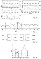
- Figure 2 shows frequency graphs representing channel selection by the RF receiver 100 of Figure 1 .
- the RF signal comprises neighbouring sub-bands SB1 and SB2, which for example correspond to one communications standard, and neighbouring sub-bands SB3 and SB4.
- Each sub-band for example comprises 2K channels, although in alternative embodiments one or more of the sub-bands could have a different number of channels from the others.
- the bandwidth BW IF is equal to the bandwidth of the largest sub-band.
- each sub-band comprises 10 channels, i.e. K is equal to 5.
- K is equal to at least 10, and is for example equal to approximately 50.
- Each channel is for example spaced by a frequency spacing ⁇ f CH of between 1 and 50 kHz, for example of around 10 KHz.
- a selected one of the sub-bands is transposed to the frequency band IF2 0 ⁇ K ⁇ f CH .
- each of the sub-bands SB1 to SB4 are centered on RF frequencies falling in the range 400 MHz to 3 GHz.
- the sub-bands SB1 and SB2 are centered on frequencies of approximately 400 MHz and the sub-bands SB3 and SB4 are centered on frequencies of approximately 800 MHz, although many other frequencies would be possible.
- the central frequency IF2 0 of the lower frequency band is for example in the range of 1 MHz to 10 MHz, and in one embodiment is equal to approximately 5 MHz.
- a curve 202 in Figure 2 represents the transfer function of the discrete time filter 108 of Figure 1 , which is discussed in more detail below in relation to Figure 10 .
- the central frequency of this filter is slid in order to select one of the 2K channels of the selected sub-band, and in some cases the bandwidth of the filter is adjusted.
- FIG 3A illustrates the down-converting and sampling circuit 104 of Figure 1 in more detail according to one example according to which it comprises a plurality of transposition circuits for progressively bringing a selected sub-band from its initial frequency band to the lower frequency band.
- Sampling is for example performed within either or both of the transposition circuits 302, 304, as will now be described with reference to Figures 3B to 3D .
- FIGS 3B to 3D schematically illustrate example embodiments of the transposition circuits 302 and 304. Only the principal transposition functions of these circuits are illustrated, and those skilled in the art will be capable of selecting appropriate filters for implementing these circuits.
- the transposition circuit 302 comprises a mixer 306, which mixes the input signal RF IN with a frequency signal f LORF generated based on a signal f LO from the reference oscillator 107 to generate the signal at the intermediate band IF1.
- the transposition circuit 304 comprises a sampling circuit 308 for sampling the signal at a frequency f S , equal for example to approximately four times the central frequency of the intermediate band signal IF1, and a decimator 310 for reducing the number of samples by a factor M d , and thus down-converting the intermediate frequency band IF1 to the lower frequency band IF2.
- the transposition circuit 302 comprises a sampling circuit 312, which under-samples the input signal RF IN .
- the sampling frequency f s in this case is equal, for example, to less than the central frequency f RF of the selected sub-band.
- the sampling operation thereby generates the signal at the intermediate frequency band IF1.
- the transposition circuit 304 comprises a decimator 314 for reducing the number of samples by a factor M d , and thus down-converting the intermediate frequency band IF1 to the lower frequency band IF2.
- the transposition circuit 302 comprises a sampling circuit 316, which under-samples the input signal RF IN .
- the sampling frequency f s1 is in this case equal, for example, to less than the central frequency f RF of the selected sub-band.
- the sampling operation thereby generates the signal at the intermediate band IF1.
- the transposition circuit 304 comprises a further sampling circuit 318, which for example under-samples the signal at the intermediate frequency band IF1 by applying a sampling frequency f s2 .
- the sampling frequency f s2 is for example equal to less than the central frequency IF1 0 of the intermediate frequency band IF1.
- the intermediate frequency band IF1 is thus down-converted to the lower frequency band IF2.
- Figure 4 illustrates the RF receiver 100 of Figure 1 in more detail in the case that the down-converting and sampling circuit 104 is implemented according to the embodiment of Figure 3B .
- An anti-aliasing filter 402 is for example provided between the mixer 306 and the sampling circuit 308.
- This filter 402 is for example an analog bandpass filter or it could be directly embedded in a current sampling. It provides anti-aliasing filtering at the frequency N.f s , as well as filtering of the image signal IMG IF1 .
- This filter for example has a pass band centered at the frequency IF1 0 , and a bandwidth of approximately 20 MHz.
- a discrete time filter (DTF) 404 is for example provided before the decimator 310, and provides anti-aliasing filtering for the decimation operation as well as IF1 image rejection in view of the lower frequency band IF2. This image is positioned at -IF1 0 +2IF2 0 . Furthermore, the bandwidth BW IF1 of this filter is adapted to cover the whole frequency range of the selected sub-band, in other words the frequency range 2K ⁇ f CH , so as not to filter out the signal itself. Typically, BW IF1 >2K ⁇ f CH .
- the DTF 404 is for example implemented by one or more IIR (infinite impulse response) filters and/or one or more FIR (finite impulse response) filters depending on the aliasing rejection level requirement.
- decimation and anti-aliasing stages could be added in order to further reduce the frequency f ADC at which the analog to digital converter 110 is running.
- the reference oscillator 107 is implemented by a quartz oscillator in the example of Figure 4 , although in alternative embodiments different types of oscillators could be used.
- the phase locked loop 106 for example comprises a divider 406 for dividing the frequency signal generated by the oscillator 107 by a factor R.
- the divided signal is provided to a mixer 408 for mixing it with a feedback frequency signal f FB .
- the output of the mixer 408 is coupled, for example via a variable low-pass filter 410, to a voltage controlled oscillator 412, which generates a frequency signal f PLL .
- the signal f PLL for example has its frequency divided by an integer N by a frequency divider 414 in order to generate the feedback signal f FB .
- the signal f PLL may directly provide the frequency signal f LORF to the mixer 306.
- the signal f PLL may be divided by a further frequency divider (not illustrated in Figure 4 ) to generate the signal F LORF .
- the sampling signal f s is for example generated by dividing the signal f PLL by a variable integer M by a frequency divider 416.
- both of the frequency signals f LORF and f s are for example generated using a common phase locked loop.
- the integer N is for example variable in order to provide a coarse frequency selection.
- an incremental change in the integer N results in a shift BWch of the signal f LORF equal to the bandwidth of a sub-band, i.e. 2K ⁇ f CH .
- FIG. 5A schematically illustrates parts of the RF receiver 100 of Figure 4 in yet more detail.
- the series connection of a switch 502, a band pass filter 504, low noise amplifier (LNA) 506 and further band pass filter 508 are for example coupled between the antenna 102 and the mixer 306, and form a radio front end.
- the switch 502 for example permits the antenna 102 to be used by both a receiver 100, and by a transmitter (not illustrated in the figures).
- the band pass filter 504 is an off-chip component having a pass-band of a bandwidth that is compatible with the sub-bands SB1, SB2, etc., and is typically equal to approximately 20 MHz.
- the mixer 306 comprises circuits 306A and 306B respectively receiving I and Q quadrature components of the RF signal.
- the circuit 306A mixes the I component with the frequency signal f LORF delayed by 90 degrees by a phase delay circuit 510.
- the circuit 306B mixes the Q component with the frequency signal f LORF .
- the signal f LORF is generated by dividing the frequency of the signal f PLL by an integer R', which in some embodiments is set equal to 4. Such a frequency division is advantageous as it increases the operating frequency of the VCO, leading to a higher quality factor.
- the output of the circuit 306A is for example provided to the band pass filter 402 via a variable gain amplifier 514A.
- the output of the circuit 306B is for example provided to the band pass filter 402 via a variable gain amplifier 514B.
- the sampling circuit 308 for example comprises a sampling circuit 308A for sampling the I component signal, and a further sampling circuit 308B for sampling the Q component signal.
- the decimator 310 for example comprises a decimation circuit 310A receiving the I component signal, and a decimation circuit 310B receiving the Q component signal.
- the ADC 110 for example comprises an ADC 110A for performing digital conversion of the I component signal, and an ADC 110B for performing digital conversion of the Q component signal.
- the central frequency IF1 0 of the DTF 404 is set to f s /4.
- An advantage of using a relatively high sampling frequency f s is that it relaxes the constraints on the image rejection performed by the RF filter 402.
- An advantage of using a relatively low sampling frequency f s is that it reduces the power consumption of the discrete time filters 404 and 108 and enables a lower decimation order M d to be applied by the decimator 310.
- the frequency IF2 0 is equal to IF1 0 /M d , and thus by increasing M d , the frequency IF2 0 can be reduced.
- M d is an odd integer.
- the sampling frequency f s is for example generated by the same PLL as the one used for generating the signal f LORF , such that only one frequency synthesis is performed.
- f s f PLL /M.
- the central frequency IF2 0 of the lower frequency band IF2 is the result of the down-conversion resulting from the convolution product between the Lth harmonic of f ADC and the intermediate frequency band IF1.
- the frequency of the signal f PLL generated by the phased locked loop has a finite step depending on the PLL division ratio N.
- Figure 5B shows:
- Figure 6 is a frequency diagram illustrating an example of the frequency response of the discrete time filter 404.
- This filter for example provides anti-aliasing rejection prior to decimation at multiples of the ADC frequency.
- the rejection bands BW rej-IF1 of this filter are located at IF1 0 +m ⁇ f d , with m being positive and negative integers.
- the order M d of the decimation operation is equal to 7.
- an odd value of M d is for example chosen such that the frequency IF2 0 becomes equal to ⁇ f d /4.
- the filter 404 applies the sinus cardinal function, which presents a notch at each one of the aliasing frequencies, and is thus particularly well adapted to such anti-aliasing purposes.
- the sinus cardinal function is for example implemented by an FIR (finite impulse response) filter.
- FIR finite impulse response
- IIR infinite impulse response
- FIG. 7A schematically illustrates an example embodiment of the discrete time filter 404, in which a plurality of IIR filter stages are cascaded, each IIR filter stage for example comprising one or more first order filters.
- the cascaded IIR filter stages are followed by an FIR stage.
- Such a solution has the advantage of limiting mismatch problems, by enabling a single capacitance ratio to be used long the stages of the filter.
- three IIR filters IIR1 to IIR3 are cascaded, but in alternative embodiments filter selectivity could be further increased by adding one or more further IIR filters, and/or by increasing the order of one or more of these filters or of the FIR filter.
- Figure 7B is a filter frequency response diagram representing, by a dashed line 702, an example of the response of a different type of filter to the one of Figure 7A formed by an FIR stage followed by an IIR stage, and by a solid line 704, an example of the response obtained by the filter of Figure 7A .
- a dashed line 702 an example of the response of a different type of filter to the one of Figure 7A formed by an FIR stage followed by an IIR stage
- a solid line 704 an example of the response obtained by the filter of Figure 7A .
- the filter is centered at f s /4.
- FIG. 8 schematically illustrates the discrete time filter 108 according to an example embodiment.
- This filter for example performs narrow band filtering in order to provide channel preselection among the 2K channels in a selected sub-band.
- Such a channel pre-selection is for example performed by shifting the transfer function of the filter such that the central frequency f 0 of the filter is over the desired channel.
- the central frequency IF2 0 of the lower frequency band IF2 is at approximately 4.5 MHz.
- the central frequency f 0 of the filter may slide by up to -/+0.5 MHz, in order to select a desired channel.
- the DTF 108 for example comprises two operational trans-impedance amplifiers (OTAs) 802, 804.
- OTAs operational trans-impedance amplifiers
- the circuit of Figure 8 is merely one example of implementation, and it will be apparent to those skilled in the art how to adapt the circuit of Figure 8 to implement a differential structure to provide improved dynamic range, or to implement a flip-flop structure so as to allow the clock frequency to be reduced and permit a connection to common mode to control the potential during the reset phase.
- a negative input of the OTA 802 is coupled to an input 806A of the DTF 108 receiving the I component signal VinI via a capacitor 808A of capacitance C1.
- a switch 810A is coupled between the capacitor 808A and the input 806A
- a switch 812A is coupled between the capacitor 808A and the negative input of the OTA 802, the switches 810A, 812A being controlled by a phase signal ⁇ 1.
- switches 814A, 816A, controlled by a phase signal ⁇ 2 are coupled between the respective nodes of the capacitor 808A and ground.
- the negative input of the OTA 802 is also coupled to an output of the OTA 802 via a first branch comprising a capacitor 818A of variable capacitance C3, and via a second branch comprising a capacitor 820A of variable capacitance C2 and switches 822A, 824A respectively coupling the capacitor 820A to the negative input and output of the OTA 802, the switches 822A, 824A being controlled by the phase signal ⁇ 1.
- a switch 826A, controlled by the phase signal ⁇ 2, is for example coupled across the nodes of the capacitor 820A.
- the output of the OTA 802 for example provides the output I component signal V outI of the filter 108.
- a negative input of the OTA 804 is coupled to an input 806B of the DTF 108 receiving the Q component VinQ, via a capacitor 808B of capacitance C1.
- a switch 810B is coupled between the capacitor 808B and the input 806B
- a switch 812B is coupled between the capacitor 808B and the negative input of the OTA 802, the switches 810B, 812B being controlled by a phase signal ⁇ 1.
- switches 814B, 816B, controlled by a phase signal ⁇ 2 are coupled between the respective nodes of the capacitor 808B and ground.
- the negative input of the OTA 804 is also coupled to an output of the OTA 804 via a first branch comprising a capacitor 818B of variable capacitance C3, and via a second branch comprising a capacitor 820B of variable capacitance C2 and switches 822B, 824B respectively coupling the capacitor 820B to the negative input and output of the OTA 804, the switches 822B, 824B being controlled by the phase signal ⁇ 1.
- a switch 826B, controlled by the phase signal ⁇ 2 is for example coupled across the nodes of the capacitor 820B.
- the output of the OTA 804 for example provides the output Q component signal V outQ Of the filter 108.
- the output of the OTA 802 is coupled to the negative input of the OTA 804 via a capacitor 828 of variable capacitance Cx and switches 830 and 832 respectively coupling the capacitor 828 to the output of the OTA 802 and to the negative input of the OTA 804, the switch 830 being controlled by the phase signal ⁇ 1 and the switch 832 being controlled by the phase signal ⁇ 2.
- Switches 834, 836, respectively controlled by the phase signals ⁇ 1 and ⁇ 2, are coupled between the respective nodes of the capacitor 828 and ground.
- the negative input of the OTA 802 is coupled to the output of the OTA 804 via a capacitor 848 of variable capacitance Cx and switches 850 and 852 respectively coupling the capacitor 848 to the negative input of the OTA 802 and to the output of the OTA 804, the switch 850 being controlled by the phase signal ⁇ 1 and the switch 852 being controlled by the phase signal ⁇ 2.
- Switches 854, 856, respectively controlled by the phase signals ⁇ 2 and ⁇ 1, are coupled between the respective nodes of the capacitor 848 and ground.
- the phase signals ⁇ 1 and ⁇ 2 are inserted in an alternate fashion.
- the phase signal ⁇ 1 is asserted during odd periods of a clock signal, and brought low during the even periods of the clock signal, where the phase signal ⁇ 2 is asserted during the even periods of a clock signal, and brought low during the odd periods of the clock signal.
- the use of the two OTAs 802, 804 and the two phase signals ⁇ 1 and ⁇ 2 permits the frequency of operation of the filter 108 to be divided by two with respect to the nominal frequency of the sampling signal f s .
- the DTF 108 also for example comprises a control circuit 860 receiving signals CH and BW indicating a desired channel to be selected, and a desired bandwidth of the filter, and generating corresponding selection signals S1, S2, S3 and Sx for controlling the values of the respective variable capacitances C2, C3 and Cx.
- a control circuit 860 receiving signals CH and BW indicating a desired channel to be selected, and a desired bandwidth of the filter, and generating corresponding selection signals S1, S2, S3 and Sx for controlling the values of the respective variable capacitances C2, C3 and Cx.
- all of the capacitors are variable except C1.
- the capacitor C1 could be variable and/or one or more of the other capacitors C2, C3 and Cx could be of fixed capacitance.
- Figure 9 is a graph representing the sliding frequency range of the central frequency f 0 as a function of the sum of the coefficients ⁇ + ⁇ based on the above equation. It can be seen that the central frequency f 0 can be slid in the negative direction when the sum ⁇ + ⁇ > 1.
- the value of C3, Cx and C2 can be set in order to achieve a desired central frequency f 0 of the filter 108, as determined by the sum of the coefficients ⁇ and ⁇ , and a desired bandwidth of the filter 108, as determined by the value of ⁇ .
- This has the advantage that the filter coefficients become independent of analog dispersion, meaning that the circuit is robust against technological dispersion and temperature variations.
- the following table provides examples of the integer multiples n i for each of the capacitances for central frequencies f 0 of 4.5 and 4 MHz, and for values of ⁇ of 0.967 ( ⁇ max in the table) and of 0.9157 ( ⁇ min in the table), which for example correspond respectively to bandwidths of 2*95 kHz and 2*255 kHz.
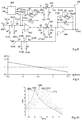
- Figure 10 is a graph representing an example of the overall transfer function Hc of the discrete time filter 404, the decimation circuit 310 and discrete time filter 108, based on the filter of Figure 8 , and assuming a sampling frequency f s of 126 MHz, an intermediate frequency IF1 0 of 31.5 MHz, a value of M d of 7, and a selective bandwidth at IF2 0 of 95 kHz.
- the pass band can be slid by increments of approximately 200 kHz in the range 31 MHz to 32 MHz.
- An advantage of performing sampling and discrete time processing is that chip area is economised when compared to a continuous time solution.
- variable band pass filter 108 An advantage of using a switched capacitor filter to implement the variable band pass filter 108 is that this provides a transfer function which is robust to technological variations because it only depends on capacitance ratios.
- An advantage of performing decimation prior to the discrete time processing is that this permits to further reduce the frequency of operation of the variable band pass filter 108 and thereby reduce power consumption.
- the frequency signal generation circuit 106 comprises a phase locked loop
Landscapes
- Engineering & Computer Science (AREA)
- Signal Processing (AREA)
- Computer Networks & Wireless Communication (AREA)
- Superheterodyne Receivers (AREA)
Abstract
Description
- The present disclosure relates to the field of radio frequency (RF) receivers, and in particular to an RF receiver capable of selecting a channel from a plurality of sub-bands.
- Mobile handsets today are often required to address multiple RF standards, such as 2G (second generation), 3G, 4G, GPS (global positioning system), WiFi (wireless fidelity), Bluetooth, etc. In order to keep manufacturing and test costs as low as possible, the number of discrete devices used to implement an RF receiver for a given standard has shrunk from several hundreds to just a few tens. There is also a move towards fully-integrated solutions.
- A classical solution is to use a super-heterodyne architecture to down-convert the RF signal to a given intermediate frequency (IF). The RF channel selection in architectures of this type could be performed using one of two different approaches.
- One approach would be to use an RF clock synthesizer to down-convert the signal to the given IF, and use an external off-chip VCO (voltage controlled oscillator) component, so as to provide a local oscillator for mixing the signal and performing down conversion. In addition, it is typical to use a quartz filter, centered at the IF, to filter out any interferers. The main limitation of this solution is that a high phase noise requirement prevents the integration of VCO itself. Furthermore, the lack of re-configurability of the off-chip component prevents several standards having different channel bandwidths from being addressed with a single component.
- An alternative approach would be to use a fixed frequency synthesizer to perform the down-conversion, and performing the filtering using a versatile filter. However, reconfigurability of the central frequency is practically impossible to achieve in such a case, and the constraint in terms of bandwidth is extremely high.
- The publication by Pui-In Mak et al. entitled "Two-step Channel Selection-A Novel Technique for Reconfigurable Multistandard Transceiver Front-Ends", IEEE transactions on circuits and systems-I: Regular papers, Vol.52, No.7, July 2005, proposes a partition of the channel selection process between RF and IF analog front-ends, such that only a coarse selection is necessary at the RF, and a fine selection is completed at the IF.
- However, while the solution described by Mak et al. provides a good trade-off between the two previously described solutions, it has drawbacks in terms of the accuracy of the frequency selection, and the quality factor that can be achieved.
- There is thus a need for an alternative receiver architecture providing channel selection with improved precision and a higher quality factor with respect to existing solutions, and for a solution permitting reconfigurability for multistandard operation.
- It is an aim of embodiments of the present description to at least partially address one or more needs in the prior art.
- According to one aspect, there is provided an RF receiver comprising: a down-converting and sampling circuit adapted to: receive an RF input signal having a signal band comprising a plurality of sub-bands, each sub-band comprising a plurality of channels separated by frequency channel spaces; perform frequency transposition and sampling to generate a discrete time signal in which a selected one of the plurality of sub-bands is brought from an initial frequency band to a lower frequency band; and a discrete time filter having a variable pass band, the central frequency (f0) of the discrete time filter being controllable to select any one of the plurality of channels of the selected sub-band.
- According to one embodiment, the discrete time filter is controllable to select a first channel of the selected sub-band by bringing the central frequency of the discrete time filter to a frequency of the first channel.
- According to one embodiment, the down-converting and sampling circuit comprises: a first transposition circuit adapted to transpose the selected sub-band from the initial frequency band to an intermediate frequency band based on a first frequency signal; a frequency signal generation circuit adapted to generate the first frequency signal based on an initial frequency signal generated as a function of the sub-band to be selected; and a second transposition circuit adapted to transpose the selected sub-band from the intermediate frequency band to the lower frequency band.
- According to one embodiment, the first transposition circuit comprises a mixer adapted to mix the RF input signal with the first frequency signal to generate an intermediate signal; the down-converting and sampling circuit comprises a sampling circuit driven by a second frequency signal to sample the intermediate signal and to generate an intermediate discrete time signal; and the second frequency signal is generated by the frequency signal generation circuit based on the initial frequency signal.
- According to one embodiment, the frequency signal generation circuit is adapted to generate the second frequency signal by dividing the initial frequency signal by an integer.
- According to one embodiment, the second transposition circuit comprises: a decimator adapted to decimate the signal at the central frequency of the intermediate frequency band and transpose the intermediate frequency band to the lower frequency band, wherein decimation decreases the sampling rate to fd=fs/Md, where fs is the frequency of the second frequency signal, and Md is the decimation order of the decimator equal to an odd integer of 3 or more; and an anti-aliasing filter adapted to perform anti-aliasing filtering prior to the decimation, wherein the anti-aliasing filter is adapted to have a pass band of a bandwidth equal to or greater than the combined bandwidth of the plurality of channels.
- According to one embodiment, the anti-aliasing filter comprises: an IIR filter stage adapted to receive the selected sub-band at the intermediate frequency band; and an FIR filter coupled to an output of the IIR filter.
- According to one embodiment, the anti-aliasing filter is configured to have: a central frequency at fs/4, where fs is the frequency of the second frequency signal; a pass bandwidth equal to or greater than the bandwidth of the selected sub-band; and rejection band characteristics rejecting the signal at IF10+m*fd, where IF10 is the central frequency of the anti-aliasing filter, m is an integer equal or greater than 1, and fd is equal to the frequency fs/Md.
- According to one embodiment, the frequency signal generation circuit comprises a phase locked loop having a feedback path comprising a division circuit adapted to divide the initial frequency signal by an integer N, wherein the value of N is adjusted based on the sub-band to be selected.
- According to one embodiment, the discrete time filter is an IIR discrete time processing filter having a transfer function Hc(z) based on the equation:

- According to one embodiment, the coefficient β is adjustable in order to control the bandwidth of the discrete time filter.
- According to one embodiment, the discrete time filter comprises a plurality of switched capacitors of which at least one has a capacitance variable in order to select one of the plurality of channels of the selected sub-band.
- According to one embodiment, the discrete time filter is adapted to have a passband bandwidth variable between a plurality of values, the plurality of switched capacitors further comprises at least one capacitor adapted to have a variable capacitance for selecting one of the plurality of passband bandwidths.
- According to one embodiment, the discrete time filter comprises: a first operational trans-impedance amplifier having a first input coupled via a first switched capacitor to a first input for receiving a first signal component from the down-converting and sampling circuit; and a second operational trans-impedance amplifier having a second input coupled via a second switched capacitor to a second input for receiving a second signal component from the down-converting and sampling circuit.
- According to one embodiment, the discrete time filter further comprises: a third capacitor coupled between the input and an output of the first operational trans-impedance amplifier; a fourth switched capacitor coupled between the input and the output of the first operational trans-impedance amplifier; a fifth capacitor coupled between the input and an output of the second operational trans-impedance amplifier; a sixth switched capacitor coupled between the input and the output of the second operational trans-impedance amplifier; a seventh switched capacitor coupled between the input of the first operational trans-impedance amplifier and the output of the second operational trans-impedance amplifier; an eighth switched capacitor coupled between the output of first operational trans-impedance amplifier and the input of the second operational trans-impedance amplifier; and a control circuit for generating selection signals for controlling the capacitance of at least one of the second, third, fourth, fifth, sixth, seventh and eighth capacitors based on the channel to be selected.
- According to a further aspect, there is provided a method of RF reception comprising: receiving by an RF receiver an RF input signal having a signal band comprising a plurality of sub-bands, each sub-band comprising a plurality of channels separated by frequency channel spaces; performing frequency transposition and sampling to generate a discrete time signal in which a selected one of the plurality of sub-bands is brought from an initial frequency band to a lower frequency band; and controlling a central frequency (f0) of a discrete time filter to select any one of the plurality of channels of the selected sub-band.
- The foregoing and other features and advantages will become apparent from the following detailed description of embodiments, given by way of illustration and not limitation with reference to the accompanying drawings, in which:
-
Figure 1 schematically illustrates an RF receiver according to an example embodiment of the present disclosure; -
Figure 2 shows frequency graphs representing channel selection by the RF receiver ofFigure 1 according to an example embodiment; -
Figure 3A schematically illustrates a down-converting and sampling circuit of the RF receiver ofFigure 1 in more detail according to an example embodiment; -
Figures 3B, 3C and 3D schematically illustrate example implementations of the circuit ofFigure 3A ; -
Figure 4 schematically illustrates the RF receiver ofFigure 1 in more detail according to an example embodiment of the present disclosure; -
Figure 5A schematically illustrates the RF receiver ofFigure 4 in yet more detail according to an example embodiment of the present disclosure; -
Figure 5B illustrates graphs representing parameters in the receiver ofFigure 4 for a range of RF frequencies according to an example embodiment; -
Figure 6 is a spectral diagram illustrating an example of the transfer function of an anti-aliasing filter ofFigures 4 and 5A ; -
Figure 7A schematically illustrates the anti-aliasing filter ofFigures 4 and 5A in more detail according to an example embodiment; -
Figure 7B is a filter frequency response diagram representing the response of FIR-IIR and IIR-FIR filters according to an example embodiment; -
Figure 8 schematically illustrates a variable discrete time band pass filter ofFigure 1 in more detail according to an example embodiment; -
Figure 9 is a graph representing frequency sliding of the variable discrete time band pass filter ofFigure 1 according to an example embodiment of the present disclosure; and -
Figure 10 is a graph representing an example of the transfer function of a decimation circuit and discrete time filter ofFigure 5A according to an example embodiment. - Throughout the present disclosure, the term "connected" is used to designate a direct electrical connection between components, whereas the term "coupled" is used to designate an electrical connection that may be direct, or may be via one or more intermediate components, such as resistors, capacitors or transistors. The term "approximately" is used to designate a range of plus or minus 10 percent of the value in question.
-
Figure 1 schematically illustrates anRF receiver 100 according to an example embodiment. - The
receiver 100 comprises anRF antenna 102 for receiving a radio frequency input signal RFIN. TheRF receiver 100 is for example capable of receiving and demodulating a channel selected from one of a plurality of sub-bands. In particular, as will be described in more detail below, the RF signal RFIN for example comprises a signal band BWRF comprising a plurality of sub-bands BWIF, each sub-band comprising 2K channels, where K is an integer equal or greater than 1. Calling the frequency spacing between each channel ΔfCH, each sub-band BWIF thus for example has a bandwidth of 2KΔfCH. - The
antenna 102 is coupled to a down-converting and sampling circuit (DOWN-CONVERTING AND SAMPLING) 104. Thecircuit 104 for example performs frequency transposition on the RF input signal in order to bring a selected one of the sub-bands from its initial frequency band down to a lower frequency band equal to IF20±KΔfCH, where IF20 is a central frequency of the lower frequency band. The central frequency IF20 for example remains at approximately the same frequency irrespective of which of the sub-bands is selected. - The down-converting and
sampling circuit 104 also for example performs sampling at a sampling frequency fs in order to generate a discrete time signal. The sampling frequency fs is for example generated by a phase-locked loop circuit (PLL CIRCUIT) 106 based on a frequency signal generated by a local oscillator (LO) 107, which is for example a VCO or the like. As represented by a dashed arrow inFigure 1 , in some embodiments thePLL circuit 106 also generates a frequency signal fLORF used by thecircuit 104 for down-converting a selected sub-band of the RF signal, for example using a mixer (not illustrated inFigure 1 ). - The down-conversion applied to the RF signal RFIN is for example variable based on the sub-band to be selected. This variation is for example achieved by varying the frequency of the signal fs and/or of the signal fLORF provided by the phase-locked
loop 106. In particular, thecircuit 106 for example receives a control signal SB indicating a sub-band to be selected, and thePLL circuit 106 generates the frequency of the signal fs and/or fLORF as a function of the control signal SB. The variation in the frequency signal fs and/or fLORF is for example performed in coarse steps. Indeed, the step size between frequency levels should permit the selection of a sub-band comprising a plurality 2K of channels, rather than any single channel. This relaxation in precision with respect to the case in which channel selection is performed on the PLL side for example permits at least part of thePLL circuit 106, such as its voltage controlled oscillator (not illustrated inFigure 1 ) to be integrated on chip. - The output of the down-converting and
sampling circuit 104 is coupled to a discrete time filter (DTF) 108, which for example has a pass band that is slid based on a channel selection signal CH. The central frequency f0 of thefilter 108 can be controlled to select one of the 2K channels of a selected sub-band. In particular, the central frequency f0 of thefilter 108 is tuned to a desired kth channel of the 2K channels forming the selected sub-band so as to perform channel selection and filter out interferers. In some embodiments, the bandwidth of thefilter 108 is also capable of being adjusted in order to cover multi-standard applications. Therefore, as represented by a dashed arrow inFigure 1 , theDTF 108 also for example receives a bandwidth selection signal BW, and is adapted to vary the bandwidth of its pass band as a function of this signal. - The
DTF 108 is for example an IIR (infinite impulse response) filter, for example implemented by a switched capacitor circuit comprising one or more variable capacitors for adjusting the central frequency and bandwidth of the DTF. In some embodiments described in more detail below, theDTF 108 is a biquad discrete time circuit comprising two OTAs (Operational Trans-impedance Amplifiers - not illustrated inFigure 1 ). - The output of the
DTF 108 is for example coupled to an analog todigital converter 110, which converts the analog discrete time signal into a digital signal. The digital signal is for example demodulated by digital processing circuits well known to those skilled in the art and not illustrated in the figures. For example, such digital processing circuits may comprise one or more of a variable integer decimation circuit, a variable base-band channel filter and a variable interpolation/non integer decimation circuit. -
Figure 2 shows frequency graphs representing channel selection by theRF receiver 100 ofFigure 1 . As illustrated, in one example, the RF signal comprises neighbouring sub-bands SB1 and SB2, which for example correspond to one communications standard, and neighbouring sub-bands SB3 and SB4. Each sub-band for example comprises 2K channels, although in alternative embodiments one or more of the sub-bands could have a different number of channels from the others. In such a case, the bandwidth BWIF is equal to the bandwidth of the largest sub-band. In the example ofFigure 2 , each sub-band comprises 10 channels, i.e. K is equal to 5. In alternative embodiments, K is equal to at least 10, and is for example equal to approximately 50. Each channel is for example spaced by a frequency spacing ΔfCH of between 1 and 50 kHz, for example of around 10 KHz. - A selected one of the sub-bands is transposed to the frequency band IF20±KΔfCH. For example, each of the sub-bands SB1 to SB4 are centered on RF frequencies falling in the
range 400 MHz to 3 GHz. In one example, the sub-bands SB1 and SB2 are centered on frequencies of approximately 400 MHz and the sub-bands SB3 and SB4 are centered on frequencies of approximately 800 MHz, although many other frequencies would be possible. The central frequency IF20 of the lower frequency band is for example in the range of 1 MHz to 10 MHz, and in one embodiment is equal to approximately 5 MHz. - A
curve 202 inFigure 2 represents the transfer function of thediscrete time filter 108 ofFigure 1 , which is discussed in more detail below in relation toFigure 10 . The central frequency of this filter is slid in order to select one of the 2K channels of the selected sub-band, and in some cases the bandwidth of the filter is adjusted. -
Figure 3A illustrates the down-converting andsampling circuit 104 ofFigure 1 in more detail according to one example according to which it comprises a plurality of transposition circuits for progressively bringing a selected sub-band from its initial frequency band to the lower frequency band. For example, thecircuit 104 comprises a transposition circuit (TRANSPO1) 302 for bringing the sub-band down to an intermediate frequency band IF1=IF10±KΔfCH, where IF10 is a central frequency of the intermediate frequency band, and a transposition circuit (TRANSPO2) 304 for bringing the intermediate frequency band down to the lower frequency band IF2=IF20±KΔfCH. Sampling is for example performed within either or both of thetransposition circuits Figures 3B to 3D . -
Figures 3B to 3D schematically illustrate example embodiments of thetransposition circuits - As illustrated in
Figure 3B , in one embodiment thetransposition circuit 302 comprises amixer 306, which mixes the input signal RFIN with a frequency signal fLORF generated based on a signal fLO from thereference oscillator 107 to generate the signal at the intermediate band IF1. Thetransposition circuit 304 comprises asampling circuit 308 for sampling the signal at a frequency fS, equal for example to approximately four times the central frequency of the intermediate band signal IF1, and adecimator 310 for reducing the number of samples by a factor Md, and thus down-converting the intermediate frequency band IF1 to the lower frequency band IF2. - As illustrated in
Figure 3C , in another embodiment thetransposition circuit 302 comprises asampling circuit 312, which under-samples the input signal RFIN. Thus the sampling frequency fs in this case is equal, for example, to less than the central frequency fRF of the selected sub-band. The sampling operation thereby generates the signal at the intermediate frequency band IF1. Thetransposition circuit 304 comprises adecimator 314 for reducing the number of samples by a factor Md, and thus down-converting the intermediate frequency band IF1 to the lower frequency band IF2. - As illustrated in
Figure 3D , in another embodiment, thetransposition circuit 302 comprises asampling circuit 316, which under-samples the input signal RFIN. Thus the sampling frequency fs1 is in this case equal, for example, to less than the central frequency fRF of the selected sub-band. The sampling operation thereby generates the signal at the intermediate band IF1. Thetransposition circuit 304 comprises afurther sampling circuit 318, which for example under-samples the signal at the intermediate frequency band IF1 by applying a sampling frequency fs2. The sampling frequency fs2 is for example equal to less than the central frequency IF10 of the intermediate frequency band IF1. The intermediate frequency band IF1 is thus down-converted to the lower frequency band IF2. - In alternative embodiments, features of the embodiments of
Figure 3B to 3D could be combined in different combinations. For example, thesampling circuit 308 anddecimator 310 ofFigure 3B could be replaced by theundersampling circuit 318. - As a further example, the
mixer 306 ofFigure 3B , or thesampling circuits Figures 3C and 3D , could be replaced by discrete time and band pass sampling circuits performing down-conversion based on the relationship fRF-0=(L+ζ×fs, where fRF-0 is the RF central frequency of the sub-band to be selected and down-converted, fs is the sampling frequency, L is the harmonic used to achieve the down conversion, and ζ = 0, 1/2, 1/4, is ratio indicating where filter of the intermediate frequency band IF1 is to be centered, respectively at fs, fs/2 or fs/4. -
Figure 4 illustrates theRF receiver 100 ofFigure 1 in more detail in the case that the down-converting andsampling circuit 104 is implemented according to the embodiment ofFigure 3B . - An
anti-aliasing filter 402 is for example provided between themixer 306 and thesampling circuit 308. Thisfilter 402 is for example an analog bandpass filter or it could be directly embedded in a current sampling. It provides anti-aliasing filtering at the frequency N.fs, as well as filtering of the image signal IMGIF1. This filter for example has a pass band centered at the frequency IF10, and a bandwidth of approximately 20 MHz. - Furthermore, a discrete time filter (DTF) 404 is for example provided before the
decimator 310, and provides anti-aliasing filtering for the decimation operation as well as IF1 image rejection in view of the lower frequency band IF2. This image is positioned at -IF10+2IF20. Furthermore, the bandwidth BWIF1 of this filter is adapted to cover the whole frequency range of the selected sub-band, in other words the frequency range 2KΔfCH, so as not to filter out the signal itself. Typically, BWIF1>2KΔfCH. TheDTF 404 is for example implemented by one or more IIR (infinite impulse response) filters and/or one or more FIR (finite impulse response) filters depending on the aliasing rejection level requirement. - While not illustrated in
Figure 4 , in some embodiments one or more further decimation and anti-aliasing stages could be added in order to further reduce the frequency fADC at which the analog todigital converter 110 is running. - The
reference oscillator 107 is implemented by a quartz oscillator in the example ofFigure 4 , although in alternative embodiments different types of oscillators could be used. The phase lockedloop 106 for example comprises adivider 406 for dividing the frequency signal generated by theoscillator 107 by a factor R. The divided signal is provided to amixer 408 for mixing it with a feedback frequency signal fFB. The output of themixer 408 is coupled, for example via a variable low-pass filter 410, to a voltage controlledoscillator 412, which generates a frequency signal fPLL. The signal fPLL for example has its frequency divided by an integer N by afrequency divider 414 in order to generate the feedback signal fFB. As shown inFigure 4 , the signal fPLL may directly provide the frequency signal fLORF to themixer 306. Alternatively, the signal fPLL may be divided by a further frequency divider (not illustrated inFigure 4 ) to generate the signal FLORF. The sampling signal fs is for example generated by dividing the signal fPLL by a variable integer M by afrequency divider 416. Thus both of the frequency signals fLORF and fs are for example generated using a common phase locked loop. - The integer N is for example variable in order to provide a coarse frequency selection. For example, in one embodiment, an incremental change in the integer N results in a shift BWch of the signal fLORF equal to the bandwidth of a sub-band, i.e. 2KΔfCH.
-
Figure 5A schematically illustrates parts of theRF receiver 100 ofFigure 4 in yet more detail. As illustrated inFigure 5A , the series connection of aswitch 502, aband pass filter 504, low noise amplifier (LNA) 506 and furtherband pass filter 508 are for example coupled between theantenna 102 and themixer 306, and form a radio front end. Theswitch 502 for example permits theantenna 102 to be used by both areceiver 100, and by a transmitter (not illustrated in the figures). In some embodiments, theband pass filter 504 is an off-chip component having a pass-band of a bandwidth that is compatible with the sub-bands SB1, SB2, etc., and is typically equal to approximately 20 MHz. Themixer 306 comprisescircuits circuit 306A mixes the I component with the frequency signal fLORF delayed by 90 degrees by aphase delay circuit 510. Thecircuit 306B mixes the Q component with the frequency signal fLORF. In the example ofFigure 5A , the signal fLORF is generated by dividing the frequency of the signal fPLL by an integer R', which in some embodiments is set equal to 4. Such a frequency division is advantageous as it increases the operating frequency of the VCO, leading to a higher quality factor. - The output of the
circuit 306A is for example provided to theband pass filter 402 via avariable gain amplifier 514A. Similarly, the output of thecircuit 306B is for example provided to theband pass filter 402 via avariable gain amplifier 514B. Thesampling circuit 308 for example comprises asampling circuit 308A for sampling the I component signal, and afurther sampling circuit 308B for sampling the Q component signal. Furthermore, thedecimator 310 for example comprises adecimation circuit 310A receiving the I component signal, and adecimation circuit 310B receiving the Q component signal. TheADC 110 for example comprises anADC 110A for performing digital conversion of the I component signal, and anADC 110B for performing digital conversion of the Q component signal. - It will be noted that the analog to
digital converter 110 runs at a frequency fADC=fs/Md, where Md is the decimation order applied by thedecimator 310. In some embodiments, the central frequency IF10 of theDTF 404 is set to fs/4. - An advantage of using a relatively high sampling frequency fs is that it relaxes the constraints on the image rejection performed by the
RF filter 402. An advantage of using a relatively low sampling frequency fs is that it reduces the power consumption of the discrete time filters 404 and 108 and enables a lower decimation order Md to be applied by thedecimator 310. - Furthermore, the frequency IF20 is equal to IF10/Md, and thus by increasing Md, the frequency IF20 can be reduced. In one embodiment, Md is an odd integer.
- In one example, the above trade-offs lead to a central sampling frequency fs0 being set to approximately 126 MHz, and the decimation order Md for example being set equal 7. Furthermore, the central frequency IF10 of the intermediate frequency band is for example selected to be approximately equal to 31.5 MHz, and thus the central ADC sampling frequency fADC0 is equal to fS0/Md=18 MHz. However, many other values would be possible.
- The sampling frequency fs is for example generated by the same PLL as the one used for generating the signal fLORF, such that only one frequency synthesis is performed. In one embodiment, fs=fPLL/M. The PLL for example runs at R' times the desired frequency, and thus fLORF=fPLL/R'.
- The intermediate frequency band IF1 could be generated based on a local oscillator frequency fLORFup that is higher than the channel frequency fRF, such that IF1up=fLORFup-fRF, or based on a local oscillator frequency fLORFdw that is lower than the channel frequency fRF, such that IF1dw=fRF-fLORFdw. It follows that:


- The central frequency IF20 of the lower frequency band IF2 is the result of the down-conversion resulting from the convolution product between the Lth harmonic of fADC and the intermediate frequency band IF1. This IF20 can be expressed as follows:

- The frequency of the signal fPLL generated by the phased locked loop has a finite step depending on the PLL division ratio N. The first down conversion provides an RF sub-band selection of K channels spaced by ΔfCH and performs a coarse channel selection:

- The value of the central frequency fRF of the selected sub-band of the RF input signal can be defined as follows based on the infradyne case of equation (4) above:

Figure 4 . The range of M is for example as follows:


-
Figure 5B shows: - a
graph 520 providing example values of the integer N for a frequency range of 380 to 430 MHz; - a
graph 522 providing example values of the integer M for the frequency range of 380 to 430 MHz; - a
graph 524 providing example values of the frequency fLORF for the frequency range of 380 to 430 MHz; - a
graph 526 providing example values of the sampling frequency fs for the frequency range of 380 to 430 MHz; - a
graph 528 providing example values of the central frequency IF10 of the intermediate frequency band IF1 for the frequency range of 380 to 430 MHz; - a
graph 530 providing example values of the central frequency IF20 of the lower frequency band IF2 for a frequency range of 380 to 430 MHz; and - a
graph 532 providing example values of the operating frequency fADC of the analog todigital converter -
Figure 6 is a frequency diagram illustrating an example of the frequency response of thediscrete time filter 404. This filter for example provides anti-aliasing rejection prior to decimation at multiples of the ADC frequency. For example, the rejection bands BWrej-IF1 of this filter are located at IF10+m·fd, with m being positive and negative integers. In the example ofFigure 6 , the order Md of the decimation operation is equal to 7. Thus the sampling frequency fs is divided into 7 frequency ranges each of width fd, where fd=fs/Md. More generally, an odd value of Md is for example chosen such that the frequency IF20 becomes equal to ±fd/4. Indeed, the frequency IF20 can be defined as follows:

- For example, the
filter 404 applies the sinus cardinal function, which presents a notch at each one of the aliasing frequencies, and is thus particularly well adapted to such anti-aliasing purposes. The sinus cardinal function is for example implemented by an FIR (finite impulse response) filter. To further increase the filter selectivity and improve rejection, the FIR filter is for example combined with an IIR (infinite impulse response) filtering function. -
Figure 7A schematically illustrates an example embodiment of thediscrete time filter 404, in which a plurality of IIR filter stages are cascaded, each IIR filter stage for example comprising one or more first order filters. The cascaded IIR filter stages are followed by an FIR stage. Such a solution has the advantage of limiting mismatch problems, by enabling a single capacitance ratio to be used long the stages of the filter. In the example ofFigure 7A , three IIR filters IIR1 to IIR3 are cascaded, but in alternative embodiments filter selectivity could be further increased by adding one or more further IIR filters, and/or by increasing the order of one or more of these filters or of the FIR filter. -
Figure 7B is a filter frequency response diagram representing, by a dashedline 702, an example of the response of a different type of filter to the one ofFigure 7A formed by an FIR stage followed by an IIR stage, and by asolid line 704, an example of the response obtained by the filter ofFigure 7A . As illustrated, advantageously the use of an IIR filter followed by an FIR filter, in that order, provides a response particularly well adapted to the sliding IF architecture described herein. Indeed, the rejection bandwidth is high and thus provides good notch filtering over the full sliding IF band. - The low pass equivalent transfer function for P cascaded IIR stages and FIR stage of order Md is given as follows:

- In some embodiments, the filter is centered at fs/4. The decimation order Md is an odd number, which means that in the decimation stage, the signal is again down-converted to a frequency which is equal to IF2=fd/4. The frequency shift from 0 to fs/4 is done by substitution on the z operator as follows:


-
Figure 8 schematically illustrates thediscrete time filter 108 according to an example embodiment. This filter for example performs narrow band filtering in order to provide channel preselection among the 2K channels in a selected sub-band. Such a channel pre-selection is for example performed by shifting the transfer function of the filter such that the central frequency f0 of the filter is over the desired channel. For example, in one embodiment, the central frequency IF20 of the lower frequency band IF2 is at approximately 4.5 MHz. For example, in the case that there are 100 channels in the selected frequency sub-band, and the channel spacing is equal to 10 KHz, the central frequency f0 of the filter may slide by up to -/+0.5 MHz, in order to select a desired channel. - The
DTF 108 for example comprises two operational trans-impedance amplifiers (OTAs) 802, 804. However, the circuit ofFigure 8 is merely one example of implementation, and it will be apparent to those skilled in the art how to adapt the circuit ofFigure 8 to implement a differential structure to provide improved dynamic range, or to implement a flip-flop structure so as to allow the clock frequency to be reduced and permit a connection to common mode to control the potential during the reset phase. - A negative input of the
OTA 802 is coupled to aninput 806A of theDTF 108 receiving the I component signal VinI via acapacitor 808A of capacitance C1. Aswitch 810A is coupled between thecapacitor 808A and theinput 806A, and aswitch 812A is coupled between thecapacitor 808A and the negative input of theOTA 802, theswitches capacitor 808A and ground. The negative input of theOTA 802 is also coupled to an output of theOTA 802 via a first branch comprising acapacitor 818A of variable capacitance C3, and via a second branch comprising acapacitor 820A of variable capacitance C2 and switches 822A, 824A respectively coupling thecapacitor 820A to the negative input and output of theOTA 802, theswitches switch 826A, controlled by the phase signal φ2, is for example coupled across the nodes of thecapacitor 820A. - The output of the
OTA 802 for example provides the output I component signal VoutI of thefilter 108. - Similarly, a negative input of the
OTA 804 is coupled to aninput 806B of theDTF 108 receiving the Q component VinQ, via acapacitor 808B of capacitance C1. Aswitch 810B is coupled between thecapacitor 808B and theinput 806B, and aswitch 812B is coupled between thecapacitor 808B and the negative input of theOTA 802, theswitches capacitor 808B and ground. The negative input of theOTA 804 is also coupled to an output of theOTA 804 via a first branch comprising acapacitor 818B of variable capacitance C3, and via a second branch comprising acapacitor 820B of variable capacitance C2 and switches 822B, 824B respectively coupling thecapacitor 820B to the negative input and output of theOTA 804, theswitches switch 826B, controlled by the phase signal φ2, is for example coupled across the nodes of thecapacitor 820B. - The output of the
OTA 804 for example provides the output Q component signal VoutQ Of thefilter 108. - The output of the
OTA 802 is coupled to the negative input of theOTA 804 via acapacitor 828 of variable capacitance Cx and switches 830 and 832 respectively coupling thecapacitor 828 to the output of theOTA 802 and to the negative input of theOTA 804, theswitch 830 being controlled by the phase signal φ1 and theswitch 832 being controlled by the phase signal φ2.Switches capacitor 828 and ground. - The negative input of the
OTA 802 is coupled to the output of theOTA 804 via acapacitor 848 of variable capacitance Cx and switches 850 and 852 respectively coupling thecapacitor 848 to the negative input of theOTA 802 and to the output of theOTA 804, theswitch 850 being controlled by the phase signal φ1 and theswitch 852 being controlled by the phase signal φ2.Switches capacitor 848 and ground. - In operation, the phase signals φ1 and φ2 are inserted in an alternate fashion. For example, the phase signal φ1 is asserted during odd periods of a clock signal, and brought low during the even periods of the clock signal, where the phase signal φ2 is asserted during the even periods of a clock signal, and brought low during the odd periods of the clock signal. The use of the two
OTAs filter 108 to be divided by two with respect to the nominal frequency of the sampling signal fs. - The
DTF 108 also for example comprises acontrol circuit 860 receiving signals CH and BW indicating a desired channel to be selected, and a desired bandwidth of the filter, and generating corresponding selection signals S1, S2, S3 and Sx for controlling the values of the respective variable capacitances C2, C3 and Cx. Indeed, in the example embodiment ofFigure 8 , all of the capacitors are variable except C1. However, in alternative embodiments, the capacitor C1 could be variable and/or one or more of the other capacitors C2, C3 and Cx could be of fixed capacitance. - The complex transfer function of the filter, for a central frequency f0, can be expressed in the following form:
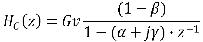


- In the circuit of
Figure 8 , the central frequency f0 of the filter slides around the nominal value IF20, centered at fd/4. Thus f0=IF20+ΔIF2, with IF20=fd/4. Thus the sum α+γ can be expressed as follows:
-
Figure 9 is a graph representing the sliding frequency range of the central frequency f0 as a function of the sum of the coefficients α+γ based on the above equation. It can be seen that the central frequency f0 can be slid in the negative direction when the sum α+γ > 1. - In the circuit of
Figure 8 , the coefficients α, γ and Gvc can be defined as follows, where GVC=Gv(1-β) represents the input voltage gain per conversion during each clock period equal to:


filter 108, as determined by the sum of the coefficients α and γ, and a desired bandwidth of thefilter 108, as determined by the value of β. It will be noted that C1 remains a degree of freedom. From this set of equations, it can be shown that the sum α+γ can be expressed as:
- In some embodiments, all of the capacitors C1, C2, C3 and Cx in
Figure 8 are equal to an integer multiple ni of a common capacitance unit Cu, where i={1,2,3,x}. This has the advantage that the filter coefficients become independent of analog dispersion, meaning that the circuit is robust against technological dispersion and temperature variations. The coefficients thus become:


- For example, for a voltage gain value Gv of 40, and for a common capacitance unit Cu of 2.2x10⁻¹³ F, the following table provides examples of the integer multiples ni for each of the capacitances for central frequencies f0 of 4.5 and 4 MHz, and for values of β of 0.967 (βmax in the table) and of 0.9157 (βmin in the table), which for example correspond respectively to bandwidths of 2*95 kHz and 2*255 kHz.
f0 βmax βmin f0+1MHz Bmax βmin f0 4.5 MHz 0.967 0.9157 4 MHz 0.967 0.9157 nfb 217 85 217 85 n 30 0 38 15 n2 217 85 180 70 Nx 210 78 207 77 n1 287 287 287 287 -
Figure 10 is a graph representing an example of the overall transfer function Hc of thediscrete time filter 404, thedecimation circuit 310 anddiscrete time filter 108, based on the filter ofFigure 8 , and assuming a sampling frequency fs of 126 MHz, an intermediate frequency IF10 of 31.5 MHz, a value of Md of 7, and a selective bandwidth at IF20 of 95 kHz. As illustrated by the six curves labelled 1002, 1004, 1006, 1008, 1010 and 1012, the pass band can be slid by increments of approximately 200 kHz in therange 31 MHz to 32 MHz. The present inventors have found that the quality factor QIF2 is equal to 23.7, and the equivalent overall quality factor at IF10 is Q{IF1-IF2}=166. This high quality factor is particularly remarkable in view of the integration constraints at the frequency of 31.5 MHz. - An advantage of performing sampling and discrete time processing is that chip area is economised when compared to a continuous time solution.
- An advantage of using a switched capacitor filter to implement the variable
band pass filter 108 is that this provides a transfer function which is robust to technological variations because it only depends on capacitance ratios. - An advantage of performing decimation prior to the discrete time processing is that this permits to further reduce the frequency of operation of the variable
band pass filter 108 and thereby reduce power consumption. - Having thus described at least one illustrative embodiment, various alterations, modifications and improvements will readily occur to those skilled in the art.
- For example, it will be apparent to those skilled in the art that while an example has been described in which the frequency
signal generation circuit 106 comprises a phase locked loop, it would be possible to use other types of circuits to generate the frequency signals fLORF and fs. - Furthermore, it will be apparent to those skilled in the art that the various features described in relation to the various embodiments could be combined, in alternative embodiments, in any combination.
Claims (16)
- An RF receiver comprising:a down-converting and sampling circuit (104) adapted to:- receive an RF input signal (RFIN) having a signal band (BWRF) comprising a plurality of sub-bands (BWIF), each sub-band comprising a plurality (2K) of channels separated by frequency channel spaces (ΔfCH);- perform frequency transposition and sampling to generate a discrete time signal in which a selected one of the plurality of sub-bands is brought from an initial frequency band to a lower frequency band (IF20±KΔfCH); anda discrete time filter (108) having a variable pass band, the central frequency (f0) of the discrete time filter being controllable to select any one of the plurality (2K) of channels of the selected sub-band.
- The RF receiver of claim 1, wherein the discrete time filter (108) is controllable to select a first channel of the selected sub-band by bringing the central frequency (f0) of the discrete time filter (108) to a frequency of the first channel.
- The RF receiver of claim 1 or 2, wherein the down-converting and sampling circuit comprises:a first transposition circuit (302) adapted to transpose the selected sub-band from the initial frequency band to an intermediate frequency band (IF10±KΔfCH) based on a first frequency signal (fLORF);a frequency signal generation circuit (106) adapted to generate the first frequency signal (fLORF) based on an initial frequency signal (fPLL) generated as a function of the sub-band to be selected; anda second transposition circuit (304) adapted to transpose the selected sub-band from the intermediate frequency band (IF10±KΔfCH) to the lower frequency band (IF20±KΔfCH).
- The RF receiver of claim 3, wherein:- the first transposition circuit (302) comprises a mixer (306) adapted to mix the RF input signal (RFIN) with the first frequency signal (fLORF) to generate an intermediate signal;- the down-converting and sampling circuit (104) comprises a sampling circuit (308) driven by a second frequency signal (fs) to sample the intermediate signal and to generate an intermediate discrete time signal; and- the second frequency signal (fs) is generated by the frequency signal generation circuit (106) based on the initial frequency signal.
- The RF receiver of claim 4, wherein the frequency signal generation circuit (106) is adapted to generate the second frequency signal (fs) by dividing the initial frequency signal (fPLL) by an integer (M).
- The RF receiver of claim 4 or 5, wherein the second transposition circuit (304) comprises:a decimator (310) adapted to decimate the signal at the central frequency (IF10) of the intermediate frequency band (IF1) and transpose the intermediate frequency band to the lower frequency band (IF20±KΔfCH), wherein decimation decreases the sampling rate to fd=fs/Md, where fs is the frequency of the second frequency signal, and Md is the decimation order of the decimator equal to an odd integer of 3 or more; andan anti-aliasing filter (404) adapted to perform anti-aliasing filtering prior to the decimation, wherein the anti-aliasing filter (404) is adapted to have a pass band of a bandwidth equal to or greater than the combined bandwidth of the plurality (2K) of channels.
- The RF receiver of claim 6, wherein the anti-aliasing filter (404) comprises:an IIR filter stage adapted to receive the selected sub-band at the intermediate frequency band (IF10±KΔfCH); andan FIR filter coupled to an output of the IIR filter.
- The RF receiver of claim 6 or 7, wherein the anti-aliasing filter (404) is configured to have:a central frequency (IF10) at fs/4, where fs is the frequency of the second frequency signal;a pass bandwidth equal to or greater than the bandwidth of the selected sub-band (IF10±KΔfCH); andrejection band characteristics rejecting the signal at IF10+m*fd, where IF10 is the central frequency (IF10) of the anti-aliasing filter (404), m is an integer equal or greater than 1, and fd is equal to the frequency fs/Md.
- The RF receiver of any of claims 3 to 8, wherein the frequency signal generation circuit (106) comprises a phase locked loop having a feedback path comprising a division circuit (414) adapted to divide the initial frequency signal by an integer N, wherein the value of N is adjusted based on the sub-band to be selected.
- The RF receiver of any of claims 1 to 9, wherein the discrete time filter (108) is an IIR discrete time processing filter having a transfer function Hc(z) based on the equation:

- The RF receiver of claim 10, wherein the coefficient β is adjustable in order to control the bandwidth of the discrete time filter (108).
- The RF receiver of any of claims 1 to 11, wherein the discrete time filter (108) comprises a plurality of switched capacitors of which at least one has a capacitance variable in order to select one of the plurality (2K) of channels of the selected sub-band.
- The RF receiver of claim 12, wherein the discrete time filter (108) is adapted to have a passband bandwidth variable between a plurality of values, the plurality of switched capacitors further comprises at least one capacitor adapted to have a variable capacitance for selecting one of the plurality of passband bandwidths.
- The RF receiver of claim 12 or 13, wherein the discrete time filter (108) comprises:a first operational trans-impedance amplifier (802) having a first input coupled via a first switched capacitor (808A) to a first input (806A) for receiving a first signal component (I) from the down-converting and sampling circuit (104); anda second operational trans-impedance amplifier (804) having a second input coupled via a second switched capacitor (808B) to a second input (806B) for receiving a second signal component (Q) from the down-converting and sampling circuit (104).
- The RF receiver of claim 14, wherein the discrete time filter (108) further comprises:a third capacitor (818A) coupled between the input and an output of the first operational trans-impedance amplifier (802);a fourth switched capacitor (820A) coupled between the input and the output of the first operational trans-impedance amplifier (802);a fifth capacitor (818B) coupled between the input and an output of the second operational trans-impedance amplifier (804);a sixth switched capacitor (820B) coupled between the input and the output of the second operational trans-impedance amplifier (804);a seventh switched capacitor (848) coupled between the input of the first operational trans-impedance amplifier (802) and the output of the second operational trans-impedance amplifier (804);an eighth switched capacitor (828) coupled between the output of first operational trans-impedance amplifier (802) and the input of the second operational trans-impedance amplifier (804); anda control circuit (860) for generating selection signals (S2 to Sx) for controlling the capacitance of at least one of the second, third, fourth, fifth, sixth, seventh and eighth capacitors based on the channel to be selected.
- A method of RF reception comprising:receiving by an RF receiver an RF input signal (RFIN) having a signal band (BWRF) comprising a plurality of sub-bands (BWIF), each sub-band comprising a plurality (2K) of channels separated by frequency channel spaces (ΔfCH);performing frequency transposition and sampling to generate a discrete time signal in which a selected one of the plurality of sub-bands is brought from an initial frequency band to a lower frequency band (IF20±KΔfCH); andcontrolling a central frequency (f0) of a discrete time filter (108) to select any one of the plurality (2K) of channels of the selected sub-band.
Applications Claiming Priority (1)
| Application Number | Priority Date | Filing Date | Title |
|---|---|---|---|
| FR1554720A FR3036902B1 (en) | 2015-05-26 | 2015-05-26 | VERSATILE RADIO RECEIVER ARCHITECTURE |
Publications (2)
| Publication Number | Publication Date |
|---|---|
| EP3098972A1 true EP3098972A1 (en) | 2016-11-30 |
| EP3098972B1 EP3098972B1 (en) | 2019-03-20 |
Family
ID=55072744
Family Applications (1)
| Application Number | Title | Priority Date | Filing Date |
|---|---|---|---|
| EP16170930.8A Not-in-force EP3098972B1 (en) | 2015-05-26 | 2016-05-23 | Versatile radio receiver architecture |
Country Status (4)
| Country | Link |
|---|---|
| US (1) | US9918310B2 (en) |
| EP (1) | EP3098972B1 (en) |
| ES (1) | ES2729660T3 (en) |
| FR (1) | FR3036902B1 (en) |
Families Citing this family (1)
| Publication number | Priority date | Publication date | Assignee | Title |
|---|---|---|---|---|
| US20230378988A1 (en) * | 2022-05-20 | 2023-11-23 | Apple Inc. | Passive radio frequency mixer with voltage gain and impedance matching |
Citations (2)
| Publication number | Priority date | Publication date | Assignee | Title |
|---|---|---|---|---|
| US20100093301A1 (en) * | 2008-10-14 | 2010-04-15 | Electronics And Telecommunications Research Institute | Heterodyne receiver using analog discrete-time signal processing and signal receiving method thereof |
| US20140194081A1 (en) * | 2012-06-21 | 2014-07-10 | Huawei Technologies Co., Ltd. | Superheterodyne Receiver |
Family Cites Families (11)
| Publication number | Priority date | Publication date | Assignee | Title |
|---|---|---|---|---|
| US8078100B2 (en) * | 2002-10-15 | 2011-12-13 | Qualcomm Incorporated | Physical layer repeater with discrete time filter for all-digital detection and delay generation |
| DE602005011164D1 (en) | 2004-10-12 | 2009-01-02 | St Microelectronics Sa | METHOD FOR TRYING AN ANALOG HIGH FREQUENCY SIGNAL |
| US7565393B2 (en) * | 2005-06-29 | 2009-07-21 | Intel Corporation | Discrete time filter having gain for digital sampling receivers |
| US7529322B2 (en) | 2005-08-26 | 2009-05-05 | University Of Macau | Two-step channel selection for wireless receiver front-ends |
| US7904048B2 (en) * | 2007-06-29 | 2011-03-08 | Texas Instruments Incorporated | Multi-tap direct sub-sampling mixing system for wireless receivers |
| US8457578B2 (en) * | 2008-12-30 | 2013-06-04 | Qualcomm Incorporated | Discrete time receiver |
| KR20100133748A (en) * | 2009-06-12 | 2010-12-22 | 삼성전자주식회사 | Discrete time filter and receiver containing it |
| FR2954628B1 (en) | 2009-12-18 | 2012-02-24 | Commissariat Energie Atomique | DEVICE AND METHOD FOR RECEIVING RF SIGNALS BASED ON A HETERODYNE ARCHITECTURE WITH UNDER-SAMPLING COMPLEX IF |
| EP2719076B1 (en) * | 2011-06-10 | 2021-08-11 | Technion R&D Foundation | Receiver, transmitter and a method for digital multiple sub-band processing |
| US8325865B1 (en) * | 2011-07-31 | 2012-12-04 | Broadcom Corporation | Discrete digital receiver |
| TWI548210B (en) * | 2014-01-13 | 2016-09-01 | 財團法人工業技術研究院 | Charge domain filter apparatus and operation method thereof |
-
2015
- 2015-05-26 FR FR1554720A patent/FR3036902B1/en not_active Expired - Fee Related
-
2016
- 2016-05-23 EP EP16170930.8A patent/EP3098972B1/en not_active Not-in-force
- 2016-05-23 ES ES16170930T patent/ES2729660T3/en active Active
- 2016-05-26 US US15/165,864 patent/US9918310B2/en not_active Expired - Fee Related
Patent Citations (2)
| Publication number | Priority date | Publication date | Assignee | Title |
|---|---|---|---|---|
| US20100093301A1 (en) * | 2008-10-14 | 2010-04-15 | Electronics And Telecommunications Research Institute | Heterodyne receiver using analog discrete-time signal processing and signal receiving method thereof |
| US20140194081A1 (en) * | 2012-06-21 | 2014-07-10 | Huawei Technologies Co., Ltd. | Superheterodyne Receiver |
Non-Patent Citations (3)
| Title |
|---|
| LATIRI A ET AL: "A reconfigurable RF sampling receiver for multistandard applications", COMPTES RENDUS - PHYSIQUE, ELSEVIER, PARIS, FR, vol. 7, no. 7, 1 September 2006 (2006-09-01), pages 785 - 793, XP024978783, ISSN: 1631-0705, [retrieved on 20060901], DOI: 10.1016/J.CRHY.2006.07.007 * |
| MAK P-I ET AL: "Two-Step Channel Selection-A Novel Technique for Reconfigurable Multistandard Transceiver Front-Ends", IEEE TRANSACTIONS ON CIRCUITS AND SYSTEMS PART I: REGULAR PAPERS, IEEE SERVICE CENTER, NEW YORK, NY, US, vol. 52, no. 7, 1 July 2005 (2005-07-01), pages 1302 - 1315, XP011136797, ISSN: 1057-7122, DOI: 10.1109/TCSI.2005.851722 * |
| PUI-IN MAK ET AL.: "Two-step Channel Selection-A Novel Technique for Reconfigurable Multistandard Transceiver Front-Ends", IEEE TRANSACTIONS ON CIRCUITS AND SYSTEMS-I: REGULAR PAPERS, vol. 52, no. 7, July 2005 (2005-07-01) |
Also Published As
| Publication number | Publication date |
|---|---|
| US20160381669A1 (en) | 2016-12-29 |
| FR3036902B1 (en) | 2018-11-16 |
| EP3098972B1 (en) | 2019-03-20 |
| ES2729660T3 (en) | 2019-11-05 |
| US9918310B2 (en) | 2018-03-13 |
| FR3036902A1 (en) | 2016-12-02 |
Similar Documents
| Publication | Publication Date | Title |
|---|---|---|
| CN103828244B (en) | Super Heterodyne Receiver and method of reseptance | |
| US8249535B2 (en) | Radio receivers | |
| US7671658B2 (en) | Mixer having frequency selection function | |
| RU2495524C2 (en) | Digital conversion method and apparatus, and signal reconfiguration method | |
| US20150214926A1 (en) | Discrete-time filter | |
| US9191127B2 (en) | Signal filtering | |
| US8340617B2 (en) | Sampling mixer, quadrature demodulator, and wireless device | |
| WO2007102459A1 (en) | Discrete time direct sampling circuit and receiver | |
| US20100093302A1 (en) | Discrete Time Direct Sampling Circuit and Receiver | |
| US20140171009A1 (en) | Radio Frequency Receiver | |
| US8208527B2 (en) | Scalable reconfigurable concurrent filter for wide-bandwidth communication | |
| EP3098972B1 (en) | Versatile radio receiver architecture | |
| US20060262230A1 (en) | Receiver if system having image rejection mixer and band-pass filter | |
| US8705675B2 (en) | Device and method for receiving RF signals based on heterodyne architecture using complex IF subsampling | |
| US11722160B2 (en) | Radio frequency receiver for carrier aggregation | |
| US20130266101A1 (en) | Sampling Receiver with Inherent Mixer Functionality | |
| US11190167B2 (en) | Discrete time charge sharing IIR bandpass filter incorporating clock phase reuse | |
| CN210075212U (en) | Software radio receiver | |
| US10103914B2 (en) | Equalizer circuit and receiving apparatus using the same | |
| KR20020068345A (en) | Single chip cmos transmitter/receiver and method of using same | |
| Folkesson et al. | Design of RF sampling receiver front-end | |
| US20120007667A1 (en) | Automatic cutoff frequency adjusting circuit and portable digital assistant | |
| CN110460346B (en) | Software radio receiver | |
| US20160329865A1 (en) | Tuner and method for tuning signals | |
| Swenson et al. | Discrete-Time Channelizers for Aeronautical Telemetry: Part I-Fixed Bandwidth |
Legal Events
| Date | Code | Title | Description |
|---|---|---|---|
| PUAI | Public reference made under article 153(3) epc to a published international application that has entered the european phase |
Free format text: ORIGINAL CODE: 0009012 |
|
| AK | Designated contracting states |
Kind code of ref document: A1 Designated state(s): AL AT BE BG CH CY CZ DE DK EE ES FI FR GB GR HR HU IE IS IT LI LT LU LV MC MK MT NL NO PL PT RO RS SE SI SK SM TR |
|
| AX | Request for extension of the european patent |
Extension state: BA ME |
|
| STAA | Information on the status of an ep patent application or granted ep patent |
Free format text: STATUS: REQUEST FOR EXAMINATION WAS MADE |
|
| 17P | Request for examination filed |
Effective date: 20170119 |
|
| RBV | Designated contracting states (corrected) |
Designated state(s): AL AT BE BG CH CY CZ DE DK EE ES FI FR GB GR HR HU IE IS IT LI LT LU LV MC MK MT NL NO PL PT RO RS SE SI SK SM TR |
|
| GRAP | Despatch of communication of intention to grant a patent |
Free format text: ORIGINAL CODE: EPIDOSNIGR1 |
|
| STAA | Information on the status of an ep patent application or granted ep patent |
Free format text: STATUS: GRANT OF PATENT IS INTENDED |
|
| INTG | Intention to grant announced |
Effective date: 20181206 |
|
| GRAJ | Information related to disapproval of communication of intention to grant by the applicant or resumption of examination proceedings by the epo deleted |
Free format text: ORIGINAL CODE: EPIDOSDIGR1 |
|
| STAA | Information on the status of an ep patent application or granted ep patent |
Free format text: STATUS: REQUEST FOR EXAMINATION WAS MADE |
|
| GRAR | Information related to intention to grant a patent recorded |
Free format text: ORIGINAL CODE: EPIDOSNIGR71 |
|
| GRAS | Grant fee paid |
Free format text: ORIGINAL CODE: EPIDOSNIGR3 |
|
| STAA | Information on the status of an ep patent application or granted ep patent |
Free format text: STATUS: GRANT OF PATENT IS INTENDED |
|
| GRAA | (expected) grant |
Free format text: ORIGINAL CODE: 0009210 |
|
| STAA | Information on the status of an ep patent application or granted ep patent |
Free format text: STATUS: THE PATENT HAS BEEN GRANTED |
|
| INTC | Intention to grant announced (deleted) | ||
| INTG | Intention to grant announced |
Effective date: 20190206 |
|
| AK | Designated contracting states |
Kind code of ref document: B1 Designated state(s): AL AT BE BG CH CY CZ DE DK EE ES FI FR GB GR HR HU IE IS IT LI LT LU LV MC MK MT NL NO PL PT RO RS SE SI SK SM TR |
|
| REG | Reference to a national code |
Ref country code: GB Ref legal event code: FG4D |
|
| REG | Reference to a national code |
Ref country code: CH Ref legal event code: EP |
|
| REG | Reference to a national code |
Ref country code: DE Ref legal event code: R096 Ref document number: 602016011191 Country of ref document: DE |
|
| REG | Reference to a national code |
Ref country code: AT Ref legal event code: REF Ref document number: 1111566 Country of ref document: AT Kind code of ref document: T Effective date: 20190415 |
|
| REG | Reference to a national code |
Ref country code: IE Ref legal event code: FG4D |
|
| REG | Reference to a national code |
Ref country code: NL Ref legal event code: MP Effective date: 20190320 |
|
| PG25 | Lapsed in a contracting state [announced via postgrant information from national office to epo] |
Ref country code: FI Free format text: LAPSE BECAUSE OF FAILURE TO SUBMIT A TRANSLATION OF THE DESCRIPTION OR TO PAY THE FEE WITHIN THE PRESCRIBED TIME-LIMIT Effective date: 20190320 Ref country code: NO Free format text: LAPSE BECAUSE OF FAILURE TO SUBMIT A TRANSLATION OF THE DESCRIPTION OR TO PAY THE FEE WITHIN THE PRESCRIBED TIME-LIMIT Effective date: 20190620 Ref country code: SE Free format text: LAPSE BECAUSE OF FAILURE TO SUBMIT A TRANSLATION OF THE DESCRIPTION OR TO PAY THE FEE WITHIN THE PRESCRIBED TIME-LIMIT Effective date: 20190320 Ref country code: LT Free format text: LAPSE BECAUSE OF FAILURE TO SUBMIT A TRANSLATION OF THE DESCRIPTION OR TO PAY THE FEE WITHIN THE PRESCRIBED TIME-LIMIT Effective date: 20190320 |
|
| REG | Reference to a national code |
Ref country code: LT Ref legal event code: MG4D |
|
| PG25 | Lapsed in a contracting state [announced via postgrant information from national office to epo] |
Ref country code: LV Free format text: LAPSE BECAUSE OF FAILURE TO SUBMIT A TRANSLATION OF THE DESCRIPTION OR TO PAY THE FEE WITHIN THE PRESCRIBED TIME-LIMIT Effective date: 20190320 Ref country code: RS Free format text: LAPSE BECAUSE OF FAILURE TO SUBMIT A TRANSLATION OF THE DESCRIPTION OR TO PAY THE FEE WITHIN THE PRESCRIBED TIME-LIMIT Effective date: 20190320 Ref country code: HR Free format text: LAPSE BECAUSE OF FAILURE TO SUBMIT A TRANSLATION OF THE DESCRIPTION OR TO PAY THE FEE WITHIN THE PRESCRIBED TIME-LIMIT Effective date: 20190320 Ref country code: NL Free format text: LAPSE BECAUSE OF FAILURE TO SUBMIT A TRANSLATION OF THE DESCRIPTION OR TO PAY THE FEE WITHIN THE PRESCRIBED TIME-LIMIT Effective date: 20190320 Ref country code: BG Free format text: LAPSE BECAUSE OF FAILURE TO SUBMIT A TRANSLATION OF THE DESCRIPTION OR TO PAY THE FEE WITHIN THE PRESCRIBED TIME-LIMIT Effective date: 20190620 Ref country code: GR Free format text: LAPSE BECAUSE OF FAILURE TO SUBMIT A TRANSLATION OF THE DESCRIPTION OR TO PAY THE FEE WITHIN THE PRESCRIBED TIME-LIMIT Effective date: 20190621 |
|
| REG | Reference to a national code |
Ref country code: AT Ref legal event code: MK05 Ref document number: 1111566 Country of ref document: AT Kind code of ref document: T Effective date: 20190320 |
|
| PG25 | Lapsed in a contracting state [announced via postgrant information from national office to epo] |
Ref country code: EE Free format text: LAPSE BECAUSE OF FAILURE TO SUBMIT A TRANSLATION OF THE DESCRIPTION OR TO PAY THE FEE WITHIN THE PRESCRIBED TIME-LIMIT Effective date: 20190320 Ref country code: IT Free format text: LAPSE BECAUSE OF FAILURE TO SUBMIT A TRANSLATION OF THE DESCRIPTION OR TO PAY THE FEE WITHIN THE PRESCRIBED TIME-LIMIT Effective date: 20190320 Ref country code: CZ Free format text: LAPSE BECAUSE OF FAILURE TO SUBMIT A TRANSLATION OF THE DESCRIPTION OR TO PAY THE FEE WITHIN THE PRESCRIBED TIME-LIMIT Effective date: 20190320 Ref country code: RO Free format text: LAPSE BECAUSE OF FAILURE TO SUBMIT A TRANSLATION OF THE DESCRIPTION OR TO PAY THE FEE WITHIN THE PRESCRIBED TIME-LIMIT Effective date: 20190320 Ref country code: AL Free format text: LAPSE BECAUSE OF FAILURE TO SUBMIT A TRANSLATION OF THE DESCRIPTION OR TO PAY THE FEE WITHIN THE PRESCRIBED TIME-LIMIT Effective date: 20190320 Ref country code: SK Free format text: LAPSE BECAUSE OF FAILURE TO SUBMIT A TRANSLATION OF THE DESCRIPTION OR TO PAY THE FEE WITHIN THE PRESCRIBED TIME-LIMIT Effective date: 20190320 Ref country code: PT Free format text: LAPSE BECAUSE OF FAILURE TO SUBMIT A TRANSLATION OF THE DESCRIPTION OR TO PAY THE FEE WITHIN THE PRESCRIBED TIME-LIMIT Effective date: 20190720 |
|
| REG | Reference to a national code |
Ref country code: ES Ref legal event code: FG2A Ref document number: 2729660 Country of ref document: ES Kind code of ref document: T3 Effective date: 20191105 |
|
| PG25 | Lapsed in a contracting state [announced via postgrant information from national office to epo] |
Ref country code: SM Free format text: LAPSE BECAUSE OF FAILURE TO SUBMIT A TRANSLATION OF THE DESCRIPTION OR TO PAY THE FEE WITHIN THE PRESCRIBED TIME-LIMIT Effective date: 20190320 Ref country code: PL Free format text: LAPSE BECAUSE OF FAILURE TO SUBMIT A TRANSLATION OF THE DESCRIPTION OR TO PAY THE FEE WITHIN THE PRESCRIBED TIME-LIMIT Effective date: 20190320 |
|
| REG | Reference to a national code |
Ref country code: CH Ref legal event code: PL |
|
| PG25 | Lapsed in a contracting state [announced via postgrant information from national office to epo] |
Ref country code: AT Free format text: LAPSE BECAUSE OF FAILURE TO SUBMIT A TRANSLATION OF THE DESCRIPTION OR TO PAY THE FEE WITHIN THE PRESCRIBED TIME-LIMIT Effective date: 20190320 Ref country code: IS Free format text: LAPSE BECAUSE OF FAILURE TO SUBMIT A TRANSLATION OF THE DESCRIPTION OR TO PAY THE FEE WITHIN THE PRESCRIBED TIME-LIMIT Effective date: 20190720 |
|
| REG | Reference to a national code |
Ref country code: DE Ref legal event code: R097 Ref document number: 602016011191 Country of ref document: DE |
|
| PLBE | No opposition filed within time limit |
Free format text: ORIGINAL CODE: 0009261 |
|
| STAA | Information on the status of an ep patent application or granted ep patent |
Free format text: STATUS: NO OPPOSITION FILED WITHIN TIME LIMIT |
|
| PG25 | Lapsed in a contracting state [announced via postgrant information from national office to epo] |
Ref country code: DK Free format text: LAPSE BECAUSE OF FAILURE TO SUBMIT A TRANSLATION OF THE DESCRIPTION OR TO PAY THE FEE WITHIN THE PRESCRIBED TIME-LIMIT Effective date: 20190320 Ref country code: CH Free format text: LAPSE BECAUSE OF NON-PAYMENT OF DUE FEES Effective date: 20190531 Ref country code: LI Free format text: LAPSE BECAUSE OF NON-PAYMENT OF DUE FEES Effective date: 20190531 Ref country code: MC Free format text: LAPSE BECAUSE OF FAILURE TO SUBMIT A TRANSLATION OF THE DESCRIPTION OR TO PAY THE FEE WITHIN THE PRESCRIBED TIME-LIMIT Effective date: 20190320 |
|
| REG | Reference to a national code |
Ref country code: BE Ref legal event code: MM Effective date: 20190531 |
|
| 26N | No opposition filed |
Effective date: 20200102 |
|
| PG25 | Lapsed in a contracting state [announced via postgrant information from national office to epo] |
Ref country code: SI Free format text: LAPSE BECAUSE OF FAILURE TO SUBMIT A TRANSLATION OF THE DESCRIPTION OR TO PAY THE FEE WITHIN THE PRESCRIBED TIME-LIMIT Effective date: 20190320 Ref country code: LU Free format text: LAPSE BECAUSE OF NON-PAYMENT OF DUE FEES Effective date: 20190523 |
|
| PG25 | Lapsed in a contracting state [announced via postgrant information from national office to epo] |
Ref country code: TR Free format text: LAPSE BECAUSE OF FAILURE TO SUBMIT A TRANSLATION OF THE DESCRIPTION OR TO PAY THE FEE WITHIN THE PRESCRIBED TIME-LIMIT Effective date: 20190320 |
|
| PG25 | Lapsed in a contracting state [announced via postgrant information from national office to epo] |
Ref country code: IE Free format text: LAPSE BECAUSE OF NON-PAYMENT OF DUE FEES Effective date: 20190523 |
|
| PG25 | Lapsed in a contracting state [announced via postgrant information from national office to epo] |
Ref country code: BE Free format text: LAPSE BECAUSE OF NON-PAYMENT OF DUE FEES Effective date: 20190531 |
|
| PG25 | Lapsed in a contracting state [announced via postgrant information from national office to epo] |
Ref country code: CY Free format text: LAPSE BECAUSE OF FAILURE TO SUBMIT A TRANSLATION OF THE DESCRIPTION OR TO PAY THE FEE WITHIN THE PRESCRIBED TIME-LIMIT Effective date: 20190320 |
|
| PG25 | Lapsed in a contracting state [announced via postgrant information from national office to epo] |
Ref country code: MT Free format text: LAPSE BECAUSE OF FAILURE TO SUBMIT A TRANSLATION OF THE DESCRIPTION OR TO PAY THE FEE WITHIN THE PRESCRIBED TIME-LIMIT Effective date: 20190320 Ref country code: HU Free format text: LAPSE BECAUSE OF FAILURE TO SUBMIT A TRANSLATION OF THE DESCRIPTION OR TO PAY THE FEE WITHIN THE PRESCRIBED TIME-LIMIT; INVALID AB INITIO Effective date: 20160523 |
|
| PGFP | Annual fee paid to national office [announced via postgrant information from national office to epo] |
Ref country code: GB Payment date: 20210514 Year of fee payment: 6 |
|
| PG25 | Lapsed in a contracting state [announced via postgrant information from national office to epo] |
Ref country code: MK Free format text: LAPSE BECAUSE OF FAILURE TO SUBMIT A TRANSLATION OF THE DESCRIPTION OR TO PAY THE FEE WITHIN THE PRESCRIBED TIME-LIMIT Effective date: 20190320 |
|
| PGFP | Annual fee paid to national office [announced via postgrant information from national office to epo] |
Ref country code: ES Payment date: 20220617 Year of fee payment: 7 Ref country code: DE Payment date: 20220519 Year of fee payment: 7 |
|
| GBPC | Gb: european patent ceased through non-payment of renewal fee |
Effective date: 20220523 |
|
| PG25 | Lapsed in a contracting state [announced via postgrant information from national office to epo] |
Ref country code: GB Free format text: LAPSE BECAUSE OF NON-PAYMENT OF DUE FEES Effective date: 20220523 |
|
| REG | Reference to a national code |
Ref country code: DE Ref legal event code: R119 Ref document number: 602016011191 Country of ref document: DE |
|
| PG25 | Lapsed in a contracting state [announced via postgrant information from national office to epo] |
Ref country code: DE Free format text: LAPSE BECAUSE OF NON-PAYMENT OF DUE FEES Effective date: 20231201 |
|
| REG | Reference to a national code |
Ref country code: ES Ref legal event code: FD2A Effective date: 20240702 |
|
| PG25 | Lapsed in a contracting state [announced via postgrant information from national office to epo] |
Ref country code: ES Free format text: LAPSE BECAUSE OF NON-PAYMENT OF DUE FEES Effective date: 20230524 |
|
| PG25 | Lapsed in a contracting state [announced via postgrant information from national office to epo] |
Ref country code: ES Free format text: LAPSE BECAUSE OF NON-PAYMENT OF DUE FEES Effective date: 20230524 |
|
| PGFP | Annual fee paid to national office [announced via postgrant information from national office to epo] |
Ref country code: FR Payment date: 20240523 Year of fee payment: 9 |
|
| PG25 | Lapsed in a contracting state [announced via postgrant information from national office to epo] |
Ref country code: FR Free format text: LAPSE BECAUSE OF NON-PAYMENT OF DUE FEES Effective date: 20250531 |