EP3098648A1 - Display device and method for repairing display device - Google Patents
Display device and method for repairing display device Download PDFInfo
- Publication number
- EP3098648A1 EP3098648A1 EP16171564.4A EP16171564A EP3098648A1 EP 3098648 A1 EP3098648 A1 EP 3098648A1 EP 16171564 A EP16171564 A EP 16171564A EP 3098648 A1 EP3098648 A1 EP 3098648A1
- Authority
- EP
- European Patent Office
- Prior art keywords
- layer
- protrusion
- display device
- pixel area
- interface
- Prior art date
- Legal status (The legal status is an assumption and is not a legal conclusion. Google has not performed a legal analysis and makes no representation as to the accuracy of the status listed.)
- Withdrawn
Links
- 238000000034 method Methods 0.000 title claims abstract description 38
- 230000002950 deficient Effects 0.000 claims abstract description 55
- 239000000758 substrate Substances 0.000 claims description 57
- 239000011159 matrix material Substances 0.000 claims description 47
- 239000000463 material Substances 0.000 claims description 46
- 239000011368 organic material Substances 0.000 claims description 38
- 229910010272 inorganic material Inorganic materials 0.000 claims description 11
- 239000011147 inorganic material Substances 0.000 claims description 11
- 229910004438 SUB2 Inorganic materials 0.000 abstract description 29
- 101100311330 Schizosaccharomyces pombe (strain 972 / ATCC 24843) uap56 gene Proteins 0.000 abstract description 29
- 101150018444 sub2 gene Proteins 0.000 abstract description 29
- 230000001678 irradiating effect Effects 0.000 abstract description 12
- 238000009413 insulation Methods 0.000 description 38
- 239000004973 liquid crystal related substance Substances 0.000 description 24
- 102100036464 Activated RNA polymerase II transcriptional coactivator p15 Human genes 0.000 description 21
- 101000713904 Homo sapiens Activated RNA polymerase II transcriptional coactivator p15 Proteins 0.000 description 21
- 229910004444 SUB1 Inorganic materials 0.000 description 21
- 230000008439 repair process Effects 0.000 description 20
- 239000011521 glass Substances 0.000 description 6
- 229910052751 metal Inorganic materials 0.000 description 6
- 239000002184 metal Substances 0.000 description 6
- 238000002844 melting Methods 0.000 description 4
- 230000008018 melting Effects 0.000 description 4
- 238000005259 measurement Methods 0.000 description 3
- 208000016169 Fish-eye disease Diseases 0.000 description 2
- 238000001652 electrophoretic deposition Methods 0.000 description 2
- 238000004519 manufacturing process Methods 0.000 description 2
- 229920001345 ε-poly-D-lysine Polymers 0.000 description 2
- 238000010521 absorption reaction Methods 0.000 description 1
- HPNSNYBUADCFDR-UHFFFAOYSA-N chromafenozide Chemical compound CC1=CC(C)=CC(C(=O)N(NC(=O)C=2C(=C3CCCOC3=CC=2)C)C(C)(C)C)=C1 HPNSNYBUADCFDR-UHFFFAOYSA-N 0.000 description 1
- 239000000470 constituent Substances 0.000 description 1
- 230000007717 exclusion Effects 0.000 description 1
- 230000005484 gravity Effects 0.000 description 1
- AMGQUBHHOARCQH-UHFFFAOYSA-N indium;oxotin Chemical compound [In].[Sn]=O AMGQUBHHOARCQH-UHFFFAOYSA-N 0.000 description 1
- 238000012986 modification Methods 0.000 description 1
- 230000004048 modification Effects 0.000 description 1
- YVTHLONGBIQYBO-UHFFFAOYSA-N zinc indium(3+) oxygen(2-) Chemical compound [O--].[Zn++].[In+3] YVTHLONGBIQYBO-UHFFFAOYSA-N 0.000 description 1
Images









Classifications
-
- G—PHYSICS
- G02—OPTICS
- G02F—OPTICAL DEVICES OR ARRANGEMENTS FOR THE CONTROL OF LIGHT BY MODIFICATION OF THE OPTICAL PROPERTIES OF THE MEDIA OF THE ELEMENTS INVOLVED THEREIN; NON-LINEAR OPTICS; FREQUENCY-CHANGING OF LIGHT; OPTICAL LOGIC ELEMENTS; OPTICAL ANALOGUE/DIGITAL CONVERTERS
- G02F1/00—Devices or arrangements for the control of the intensity, colour, phase, polarisation or direction of light arriving from an independent light source, e.g. switching, gating or modulating; Non-linear optics
- G02F1/01—Devices or arrangements for the control of the intensity, colour, phase, polarisation or direction of light arriving from an independent light source, e.g. switching, gating or modulating; Non-linear optics for the control of the intensity, phase, polarisation or colour
- G02F1/13—Devices or arrangements for the control of the intensity, colour, phase, polarisation or direction of light arriving from an independent light source, e.g. switching, gating or modulating; Non-linear optics for the control of the intensity, phase, polarisation or colour based on liquid crystals, e.g. single liquid crystal display cells
- G02F1/1306—Details
- G02F1/1309—Repairing; Testing
-
- G—PHYSICS
- G02—OPTICS
- G02F—OPTICAL DEVICES OR ARRANGEMENTS FOR THE CONTROL OF LIGHT BY MODIFICATION OF THE OPTICAL PROPERTIES OF THE MEDIA OF THE ELEMENTS INVOLVED THEREIN; NON-LINEAR OPTICS; FREQUENCY-CHANGING OF LIGHT; OPTICAL LOGIC ELEMENTS; OPTICAL ANALOGUE/DIGITAL CONVERTERS
- G02F1/00—Devices or arrangements for the control of the intensity, colour, phase, polarisation or direction of light arriving from an independent light source, e.g. switching, gating or modulating; Non-linear optics
- G02F1/01—Devices or arrangements for the control of the intensity, colour, phase, polarisation or direction of light arriving from an independent light source, e.g. switching, gating or modulating; Non-linear optics for the control of the intensity, phase, polarisation or colour
- G02F1/13—Devices or arrangements for the control of the intensity, colour, phase, polarisation or direction of light arriving from an independent light source, e.g. switching, gating or modulating; Non-linear optics for the control of the intensity, phase, polarisation or colour based on liquid crystals, e.g. single liquid crystal display cells
- G02F1/133—Constructional arrangements; Operation of liquid crystal cells; Circuit arrangements
- G02F1/1333—Constructional arrangements; Manufacturing methods
- G02F1/1335—Structural association of cells with optical devices, e.g. polarisers or reflectors
- G02F1/133509—Filters, e.g. light shielding masks
- G02F1/133512—Light shielding layers, e.g. black matrix
-
- G—PHYSICS
- G02—OPTICS
- G02F—OPTICAL DEVICES OR ARRANGEMENTS FOR THE CONTROL OF LIGHT BY MODIFICATION OF THE OPTICAL PROPERTIES OF THE MEDIA OF THE ELEMENTS INVOLVED THEREIN; NON-LINEAR OPTICS; FREQUENCY-CHANGING OF LIGHT; OPTICAL LOGIC ELEMENTS; OPTICAL ANALOGUE/DIGITAL CONVERTERS
- G02F1/00—Devices or arrangements for the control of the intensity, colour, phase, polarisation or direction of light arriving from an independent light source, e.g. switching, gating or modulating; Non-linear optics
- G02F1/01—Devices or arrangements for the control of the intensity, colour, phase, polarisation or direction of light arriving from an independent light source, e.g. switching, gating or modulating; Non-linear optics for the control of the intensity, phase, polarisation or colour
- G02F1/13—Devices or arrangements for the control of the intensity, colour, phase, polarisation or direction of light arriving from an independent light source, e.g. switching, gating or modulating; Non-linear optics for the control of the intensity, phase, polarisation or colour based on liquid crystals, e.g. single liquid crystal display cells
- G02F1/133—Constructional arrangements; Operation of liquid crystal cells; Circuit arrangements
- G02F1/1333—Constructional arrangements; Manufacturing methods
- G02F1/133305—Flexible substrates, e.g. plastics, organic film
-
- G—PHYSICS
- G02—OPTICS
- G02F—OPTICAL DEVICES OR ARRANGEMENTS FOR THE CONTROL OF LIGHT BY MODIFICATION OF THE OPTICAL PROPERTIES OF THE MEDIA OF THE ELEMENTS INVOLVED THEREIN; NON-LINEAR OPTICS; FREQUENCY-CHANGING OF LIGHT; OPTICAL LOGIC ELEMENTS; OPTICAL ANALOGUE/DIGITAL CONVERTERS
- G02F1/00—Devices or arrangements for the control of the intensity, colour, phase, polarisation or direction of light arriving from an independent light source, e.g. switching, gating or modulating; Non-linear optics
- G02F1/01—Devices or arrangements for the control of the intensity, colour, phase, polarisation or direction of light arriving from an independent light source, e.g. switching, gating or modulating; Non-linear optics for the control of the intensity, phase, polarisation or colour
- G02F1/13—Devices or arrangements for the control of the intensity, colour, phase, polarisation or direction of light arriving from an independent light source, e.g. switching, gating or modulating; Non-linear optics for the control of the intensity, phase, polarisation or colour based on liquid crystals, e.g. single liquid crystal display cells
- G02F1/133—Constructional arrangements; Operation of liquid crystal cells; Circuit arrangements
- G02F1/1333—Constructional arrangements; Manufacturing methods
- G02F1/1335—Structural association of cells with optical devices, e.g. polarisers or reflectors
- G02F1/133509—Filters, e.g. light shielding masks
- G02F1/133514—Colour filters
-
- G—PHYSICS
- G02—OPTICS
- G02F—OPTICAL DEVICES OR ARRANGEMENTS FOR THE CONTROL OF LIGHT BY MODIFICATION OF THE OPTICAL PROPERTIES OF THE MEDIA OF THE ELEMENTS INVOLVED THEREIN; NON-LINEAR OPTICS; FREQUENCY-CHANGING OF LIGHT; OPTICAL LOGIC ELEMENTS; OPTICAL ANALOGUE/DIGITAL CONVERTERS
- G02F1/00—Devices or arrangements for the control of the intensity, colour, phase, polarisation or direction of light arriving from an independent light source, e.g. switching, gating or modulating; Non-linear optics
- G02F1/01—Devices or arrangements for the control of the intensity, colour, phase, polarisation or direction of light arriving from an independent light source, e.g. switching, gating or modulating; Non-linear optics for the control of the intensity, phase, polarisation or colour
- G02F1/13—Devices or arrangements for the control of the intensity, colour, phase, polarisation or direction of light arriving from an independent light source, e.g. switching, gating or modulating; Non-linear optics for the control of the intensity, phase, polarisation or colour based on liquid crystals, e.g. single liquid crystal display cells
- G02F1/133—Constructional arrangements; Operation of liquid crystal cells; Circuit arrangements
- G02F1/136—Liquid crystal cells structurally associated with a semi-conducting layer or substrate, e.g. cells forming part of an integrated circuit
- G02F1/1362—Active matrix addressed cells
- G02F1/136259—Repairing; Defects
-
- G—PHYSICS
- G02—OPTICS
- G02F—OPTICAL DEVICES OR ARRANGEMENTS FOR THE CONTROL OF LIGHT BY MODIFICATION OF THE OPTICAL PROPERTIES OF THE MEDIA OF THE ELEMENTS INVOLVED THEREIN; NON-LINEAR OPTICS; FREQUENCY-CHANGING OF LIGHT; OPTICAL LOGIC ELEMENTS; OPTICAL ANALOGUE/DIGITAL CONVERTERS
- G02F1/00—Devices or arrangements for the control of the intensity, colour, phase, polarisation or direction of light arriving from an independent light source, e.g. switching, gating or modulating; Non-linear optics
- G02F1/01—Devices or arrangements for the control of the intensity, colour, phase, polarisation or direction of light arriving from an independent light source, e.g. switching, gating or modulating; Non-linear optics for the control of the intensity, phase, polarisation or colour
- G02F1/13—Devices or arrangements for the control of the intensity, colour, phase, polarisation or direction of light arriving from an independent light source, e.g. switching, gating or modulating; Non-linear optics for the control of the intensity, phase, polarisation or colour based on liquid crystals, e.g. single liquid crystal display cells
- G02F1/133—Constructional arrangements; Operation of liquid crystal cells; Circuit arrangements
- G02F1/1333—Constructional arrangements; Manufacturing methods
- G02F1/133345—Insulating layers
-
- G—PHYSICS
- G02—OPTICS
- G02F—OPTICAL DEVICES OR ARRANGEMENTS FOR THE CONTROL OF LIGHT BY MODIFICATION OF THE OPTICAL PROPERTIES OF THE MEDIA OF THE ELEMENTS INVOLVED THEREIN; NON-LINEAR OPTICS; FREQUENCY-CHANGING OF LIGHT; OPTICAL LOGIC ELEMENTS; OPTICAL ANALOGUE/DIGITAL CONVERTERS
- G02F1/00—Devices or arrangements for the control of the intensity, colour, phase, polarisation or direction of light arriving from an independent light source, e.g. switching, gating or modulating; Non-linear optics
- G02F1/01—Devices or arrangements for the control of the intensity, colour, phase, polarisation or direction of light arriving from an independent light source, e.g. switching, gating or modulating; Non-linear optics for the control of the intensity, phase, polarisation or colour
- G02F1/13—Devices or arrangements for the control of the intensity, colour, phase, polarisation or direction of light arriving from an independent light source, e.g. switching, gating or modulating; Non-linear optics for the control of the intensity, phase, polarisation or colour based on liquid crystals, e.g. single liquid crystal display cells
- G02F1/133—Constructional arrangements; Operation of liquid crystal cells; Circuit arrangements
- G02F1/136—Liquid crystal cells structurally associated with a semi-conducting layer or substrate, e.g. cells forming part of an integrated circuit
- G02F1/1362—Active matrix addressed cells
- G02F1/136254—Checking; Testing
-
- G—PHYSICS
- G02—OPTICS
- G02F—OPTICAL DEVICES OR ARRANGEMENTS FOR THE CONTROL OF LIGHT BY MODIFICATION OF THE OPTICAL PROPERTIES OF THE MEDIA OF THE ELEMENTS INVOLVED THEREIN; NON-LINEAR OPTICS; FREQUENCY-CHANGING OF LIGHT; OPTICAL LOGIC ELEMENTS; OPTICAL ANALOGUE/DIGITAL CONVERTERS
- G02F2201/00—Constructional arrangements not provided for in groups G02F1/00 - G02F7/00
- G02F2201/50—Protective arrangements
- G02F2201/506—Repairing, e.g. with redundant arrangement against defective part
- G02F2201/508—Pseudo repairing, e.g. a defective part is brought into a condition in which it does not disturb the functioning of the device
Definitions
- the invention relates generally to a display device and a method for repairing the display device.
- an organic light emitting display In general, an organic light emitting display, a liquid crystal display (“LCD”), a plasma display panel, and the like are representative examples of a flat panel display.
- LCD liquid crystal display
- plasma display panel and the like are representative examples of a flat panel display.
- the LCD includes a first substrate, a liquid crystal layer, electrodes driving the liquid crystal layer, wires supplying current to the electrodes, a second substrate, and a plurality of insulation layers provided between the first substrate and the second substrate.
- Such an LCD displays predetermined images by forming a plurality of pixel areas, each being the minimum unit for displaying an image, with a first substrate, a liquid crystal layer, electrodes driving the liquid crystal layer, wires supplying current to the electrodes, a second substrate, and a plurality of insulation layers provided between the first substrate and the second substrate.
- the invention sets out to provide a display device in which a defective pixel area is repaired, and a method for easily repairing a defective pixel area of a display device.
- One embodiment of the invention provides a method for repairing a display device including a defective pixel area where a failure has occurred.
- the method include: irradiating a first laser beam to a first interface provided between a first layer and a second layer that contact each other corresponding to the defective pixel area to form a protrusion-depression surface in one or more surfaces of the first layer and the second layer that form the first interface; and irradiating a second laser beam to the protrusion-depression surfaces provided in one or more surfaces of the first and second layers to burn the protrusion-depression surface.
- the method further includes flowing a black material melted from a black matrix that neighbors the first interface to the protrusion-depression surface, wherein the irradiating the second laser beam may further include burning the black material provided in the protrusion-depression surface.
- the irradiating the first laser beam may further include forming a protrusion-depression surface in one or more surfaces of the second layer and a third layer contacting each other and thus forming a second interface
- the irradiating the second laser beam may further include burning the protrusion-depression surface provided in one or more surfaces of the second layer and the third layer.
- the method may further include flowing a black material melted from a black matrix that is disposed neighboring the second interface to the protrusion-depression surface, and the irradiating the second laser beam may further include burning the black material provided in the protrusion-depression surface.
- the irradiating the first laser beam may further include forming a protrusion-depression surface in one or more surfaces of the third layer and a fourth layer that contact each other and thus form a third interface
- the irradiating the second laser beam may further include burning the protrusion-depression surface provided in one or more surfaces of the third layer and the fourth layer.
- Another embodiment of the invention provides a display device including a first pixel area where a failure has occurred and a second pixel area neighboring the first pixel area.
- the display device includes a first layer and a second layer contacting each other and thus forming a first interface, wherein a burned protrusion-depression surface is provided in one or more surfaces of the first layer and the second layer that form the first interface corresponding to the first pixel area.
- the first layer may be a substrate and the second layer may include an organic material.
- the second layer may be a color filter.
- the protrusion-depression surface may be provided in the second layer.
- the first layer may include an inorganic material
- the second layer comprises an organic material
- the protrusion-depression surface may be provided in the second layer.
- the display device may further include a black matrix provided neighboring the first interface and extended to the protrusion-depression surface, wherein at least a part of the black matrix extended to the protrusion-depression surface is burned.
- the display device may further include a third layer contacting the second layer and thus forming a second interface, wherein a burned protrusion-depression surface may be provided in one or more surfaces of the second and third layers forming the second interface corresponding to the first pixel area.
- the second layer and the third layer respectively may include an organic material.
- the second layer is may be color filter.
- the protrusion-depression surface may be provided in each of the second and third layers.
- the second layer may include an organic material
- the third layer may include a transparent conductive oxide
- the protrusion-depression surface may be provided in the second layer.
- the display device may further include a black matrix provided neighboring the second interface and extended to the protrusion-depression surface, wherein at least a part of the black matrix extended to the protrusion-depression surface may be burned.
- the display device may further include a fourth layer contacting the third layer and thus forming a third interface, wherein a burned protrusion-depression surface may be provided in one or more surfaces of the third and fourth layers forming the third interface corresponding to the first pixel area.
- a display device in which a defective pixel area is repaired and a method for repairing a defective pixel area of the display device can be provided.
- the word “comprise” and variations such as “comprises” or “comprising” will be understood to imply the inclusion of stated elements but not the exclusion of any other elements.
- the word “on” means positioning on or below the object portion, but does not essentially mean positioning on the upper side of the object portion based on a gravity direction.
- relative terms such as “lower” or “bottom” and “upper” or “top,” may be used herein to describe one element's relationship to another element as illustrated in the Figures. It will be understood that relative terms are intended to encompass different orientations of the device in addition to the orientation depicted in the Figures. For example, if the device in one of the figures is turned over, elements described as being on the “lower” side of other elements would then be oriented on “upper” sides of the other elements. The exemplary term “lower,” can therefore, encompasses both an orientation of “lower” and “upper,” depending on the particular orientation of the figure.
- Embodiments of the invention are described herein with reference to cross section illustrations that are schematic illustrations of idealized embodiments. As such, variations from the shapes of the illustrations as a result, for example, of manufacturing techniques and/or tolerances, are to be expected. Thus, embodiments described herein should not be construed as limited to the particular shapes of regions as illustrated herein but are to include deviations in shapes that result, for example, from manufacturing. For example, a region illustrated or described as flat may, typically, have rough and/or nonlinear features. Moreover, sharp angles that are illustrated may be rounded. Thus, the regions illustrated in the figures are schematic in nature and their shapes are not intended to illustrate the precise shape of a region and are not intended to limit the scope of the present claims.
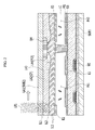
- FIG. 1 illustrates a flowchart of a repair method of a display device according to an embodiment.
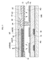
- FIGS. 2 to 4 illustrate cross-sectional views of the repair method of the display device according to the embodiment.
- a surface having protrusion-depression is formed in an interface by irradiating a first laser beam corresponding to a defective pixel area (S110).
- the display device includes a plurality of pixel areas, each being a minimum unit for displaying an image, and the plurality of pixel areas include a first pixel area PX1 and a second pixel area PX2.
- the display device includes a first substrate SUB1, a wire WI, a first electrode E1, a first alignment layer PI1, a liquid crystal layer LC, a fourth layer LA4 which is a second alignment layer PI2, a second electrode E2, a third layer LA3 which is an insulation layer, a second layer LA2 which is a color filter CF, a black matrix BM, and a first layer LA1 which is a second substrate SUB2.
- the first substrate SUB1, the wiring WI, the first electrode E1, the first alignment layer PI1, the liquid crystal layer LC, the fourth layer LA4 which is the second alignment layer PI2, the second electrode E2, the third layer LA3 which is the insulation layer, the second layer LA2 which is the color filter CF, the black matrix BM, and the first layer LA1 which is the second substrate SUB2 may have various structures known to a person skilled in the art, and thus the structure shown in FIG. 2 is not restrictive.
- the first laser beam LB1 is irradiated to a first interface IL1 between the first layer LA1 which is the second substrate SUB2 and the second layer LA2 which is the color filter CF.
- the first layer LA1 and the second layer LA2 contact each other corresponding to the first pixel area PX1 which is the defective pixel area.
- the first laser beam LB1 may scan the entire area of the first pixel area PX1 with various routes in a plane.
- the first laser beam LB1 may be irradiated to one of the first interface IL1 between the first layer LA1 and the second layer LA2 that contact each other, a second interface IL2 between the second layer LA2 and the third layer LA3 that contact each other, and a third interface IL3 between the third layer LA3 and the fourth layer LA4 that contact each other, and a surface of one of layers including an organic material among the first, second, third, and fourth layers LA1, LA2, LA3, and LA4 is formed as a surface IS having protrusion-depression caused by energy from the first laser beam LB1.
- one or more surfaces of the first layer LA1 and the second layer LA2 forming the first interface IL1 between the first layer LA1 and the second layer LA2 that contact each other is formed as the surface IS having protrusion-depression
- one or more surfaces of the second layer LA2 and the third layer LA3 forming the second interface IL2 between the second layer LA2 and the third layer LA3 that contact each other is formed as the surface IS having protrusion-depression
- one or more surfaces of the third layer LA3 and the fourth layer LA4 forming the third interface IL3 between the third layer LA3 and the fourth layer LA4 that contact each other is formed as the surface IS having protrusion-depression.
- the energy from the first laser beam LB1 is transferred not only to the first interface IL1 but also to the third interface IL3 that neighbors the second interface IL2 while at the same time the first laser beam LB1 passes through the first interface IL1 such that a surface of one or more layers including an organic material among the first, second, third, and fourth layers LA1, LA2, LA3, and LA4 is provided as the surface IS having protrusion-depression, for example.
- the first layer LA1 includes the second substrate SUB2 that may include an inorganic material, metal, and glass
- the second layer LA2 includes the color filter CF including an organic material
- the third layer LA3 includes an insulation layer including an organic material
- the fourth layer LA4 includes the second alignment layer PI2 including an organic material such that the surface of each of the second, third, and fourth layers LA2, LA3, and LS4 is provided as the surface IS having the protrusion-depression by the first laser beam LB1.
- Gaps GA are respectively defined between the first interface IL1, the second interface IL2, and the third interface IL3 where the surfaces IS having protrusion-depression are provided.
- lateral surfaces of the second layer LA2 where the first interface IL1 and the second interface IL2 are provided are provided as the surfaces IS having protrusion-depression
- lateral surfaces of the third layer LA3 where the second interface IL2 and the third interface IL3 are provided are provided as the surfaces IS having protrusion-depression
- one surface of the fourth layer LA4 where the third interface IL3 is provided is provided as the surface IS having protrusion-depression.
- the surface IS having protrusion-depression is burnt by irradiating a second laser beam LB2 thereto (S120 in FIG. 1 ).
- the second laser beam LB2 is irradiated to one or more surfaces IS having protrusion-depression among the first layer LA1 and the second layer LA2 corresponding to the first pixel area PX1, which is a defective pixel area, so as to burn the surface IS having protrusion-depression.
- the surface IS having protrusion-depression may be carbonized while being burnt by irradiation of the second laser beam LB2, and accordingly, the first pixel area PX1, which is the defective pixel area, may be recognized as a dark spot.
- the second laser beam LB2 may scan the entire area of the first pixel area PX1 with various routes in a plane.
- the second laser beam LB2 may be irradiated to one or more surfaces IS having protrusion-depression among the first layer LA1, the second layer LA2, the third layer LA3, and the fourth layer LA4, and the protrusion-depression surface IS provided in the surface of one or more layers of the second layer LA2, the third layer LA3, and the fourth layer LA4 including an organic material may be carbonized while being burnt by energy of the second laser beam LB2.
- the protrusion-depression surface IS provided in one or more surfaces of the first layer LA1 and the second layer LA2 is burnt by the second laser beam LB2
- the protrusion-depression surface IS provided in one or more surfaces of the second layer LA2 and the third layer LA3 is burnt
- the protrusion-depression surface IS provided in one or more surfaces of the third layer LA3 and the fourth layer LA4 is burnt, and accordingly each protrusion-depression surface IS may be carbonized.
- the second laser beam LB2 when the second laser beam LB2 is irradiated to the protrusion-depression surface IS of the third layer LA3, the second laser beam LB2 passes the protrusion-depression surface IS of one or more of the first layer LA1 and the second layer LA2 and at the same time the energy from the second laser beam LB2 is transferred to the protrusion-depression surface IS of the fourth layer LA4 that neighbors the third layer LA3 such that one or more protrusion-depression surfaces IS including an organic material among the first layer LA1, the second layer LA2, the third layer LA3, and the fourth layer LA4 may be burnt and thus carbonized by the energy of the second laser beam LB2, for example.
- the protrusion-depression surface IS occupies much more surface area compared to a flat surface in the same space, and thus the protrusion-depression surface IS may be easily carbonized by being burnt by the energy of the second laser beam LB2.
- the protrusion-depression surface IS is provided in each of the second layer LA2, the third layer LA3, and the fourth layer LA4, and the respective protrusion-depression surfaces IS may be burnt and then carbonized by the energy of the second laser beam LB2.
- the protrusion-depression surfaces IS provided in lateral sides of the second layer LA2 the protrusion-depression surfaces IS provided in lateral sides of the third layer LA3, and the protrusion-depression surface IS provided in one side of the fourth layer LA4 may be respectively burnt and then carbonized by the second laser beam LB2.
- the surfaces of the second layer LA2, the third layer LA3, and the fourth layer LA4 among the first layer LA1, the second layer LA2, the third layer LA3, and the fourth layer LA4 that correspond to the first pixel area PX1, which is a defective pixel area, among the first pixel area PX1 and the second pixel area pX2 of the display device are respectively provided as the protrusion-depression surfaces IS, and the protrusion-depression surfaces IS are burnt to be carbonized such that the first pixel area PX1, which is the defective pixel area, is recognized as a dark spot, thereby preventing the first pixel area PX1 from being viewed. That is, according to the repair method of the display device, a defective pixel area may be repaired by irradiation of a laser beam twice.
- a liquid crystal display (LCD) will be described as a display device using the above-state repairing method, but the invention is not so limited.
- a repairing method of a display device according to another exemplary embodiment may be used in various display devices such as an organic light emitting diode display (“OLED”), plasma displays (“PDs”), field emission displays (“FEDs”), electrophoretic displays (“EPDs”), electrowetting displays (“EWDs”), and the like as long as one or more layers among two layers contacting each other and thus forming an interface include an organic material.
- OLED organic light emitting diode display
- PDs plasma displays
- FEDs field emission displays
- EPDs electrophoretic displays
- EWDs electrowetting displays
- a display device to be described hereinafter according to another embodiment of the invention may be a display device repaired by the above-described repair method of the display device.
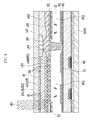
- FIG. 5 illustrates a cross-sectional view of a display device according to another embodiment of the invention.
- a display device includes a plurality of pixel areas, each being a minimum unit for displaying an image, and the plurality of pixel areas include a first pixel area PX1, which is a defective pixel area where an error has occurred, and a second pixel area PX2, which is a normal pixel area where no error has occurred.
- the display device includes a first substrate SUB1, a wire WI, a first electrode E1, a first alignment layer PI1, a liquid crystal layer LC, a fourth layer LA4 which is a second alignment layer PI2, a second electrode E2, a third layer LA3 which is an insulation layer, a second layer LA2 which is a color filter CF, a black matrix BM, and a first layer LA1 which is a second substrate SUB2, and they are sequentially layered.
- the first substrate SUB1, the wire WI, the first electrode E1, the first alignment layer PI1, the liquid crystal layer LC, the fourth layer LA4 which is the second alignment layer PI2, the second electrode E2, the third layer LA3 which is the insulation layer, the second layer LA2 which is the color filter CF, the black matrix BM, and the first layer LA1 which is the second substrate SUB2 may have various structures known to a person skilled in the art, and thus the structure shown in FIG. 5 is not restrictive.
- one or more surfaces of the first and second layers LA1 and LA2 being in contact with each other and thus forming a first interface are provided as a burned protrusion-depression surface IS corresponding to the first pixel area PX1
- one or more surfaces of the second and third layers LA2 and LA3 being in contact with each other and thus forming a second interface are provided as a burned protrusion-depression surface IS corresponding to the first pixel area PX1
- one or more surfaces of the third and fourth layers LA3 and LA4 being in contact with each other and thus forming a third interface are provided as a burned protrusion-depression surface IS corresponding to the first pixel area PX1.
- the first layer LA1 is provided as a second substrate SUB2 that may include an inorganic material, a metal, glass, and the like
- the second layer LA2 is provided as a color filter CF including an organic material
- the third layer LA3 is provided as an insulation layer including an organic material
- the fourth layer LA4 is provided as a second alignment layer PI2 including an organic material such that a surface of each of the second, third, and fourth layers LA2, LA3, and LA4 is provided as a burned protrusion-depression surface IS.
- the protrusion-depression surfaces IS of the first, second, third, and fourth layers LA1, LA2, LA3, and LA4 define gaps GA between the first and second layers LA1 and LA2, between the second and third layers LA2 and LA3, and between the third and fourth layers LA3 and LA4, respectively.
- lateral surfaces of the second layer LA2 respectively forming the first interface and the second interface are provided as the burned protrusion-depression surfaces IS
- lateral surfaces of the third layer LA3 respectively forming the second interface and the third interface are provided as the burned protrusion-depression surfaces IS
- one surface of the fourth layer LA4 forming the third interface is provided as the burned protrusion-depression surface IS. That is, the protrusion-depression surfaces IS burned corresponding to the first pixel area PX1 are viewed as dark, and accordingly, the first pixel area PX1 is viewed as a dark spot.
- surfaces of the second, third, and fourth layers LA2, LA3, and LA4 among the first layer LA1, the second layer LA2, the third layer LA3, and the fourth layer LA4 that correspond to the first pixel area PX1, which is a defective pixel area where a failure has occurred among the first pixel area PX1 and the second pixel area PX2, are respectively provided as the burned protrusion-depression surfaces IS so that the first pixel area PX1, which is a defective pixel area, is viewed as a dark spot, and thus the first pixel area PX1 may be prevented from being viewed when other pixel areas among the plurality of pixel areas display an image. That is, a display device of which the first pixel area PX1, which is a defective pixel area, is repaired to be a dark spot by the burned protrusion-depression surface IS may be provided.
- the display device is exemplarily described as an LCD, but any display device of which one or more layers among two layers forming an interface by being in contact with each other includes an organic material is applicable.
- OLED, PDs, FEDs, EPDs, and EWDs are applicable, for example.
- FIG. 6 is a flowchart illustrating a repairing method of a display device according to another embodiment of the invention.
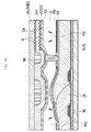
- FIGS. 7 and 8 illustrate cross-sectional views provided for description of the repairing method of the display device according to the other embodiment of the invention.
- a first laser beam is irradiated to an interface corresponding to a defective pixel area to form a protrusion-depression surface (S210).
- the display device includes a plurality of pixel areas, each being the minimum unit for displaying an image, and the plurality of pixel areas include a first pixel area PX1 and a second pixel area PX2.
- the display device includes a first substrate SUB1, a wire WI, a first electrode E1, a first alignment layer PI1, a liquid crystal layer LC, a fourth layer LA4 which is a second alignment layer PI2, a third layer LA3 which is an insulation layer, a second layer LA2 which is a color filter CF, a black matrix BM, and a first layer LA1 which is a second substrate SUB2.
- the first substrate SUB1, the wire WI, the first electrode E1, the first alignment layer PI1, the liquid crystal layer LC, the fourth layer LA4 which is the second alignment layer PI2, the second electrode E2, the third layer LA3 which is the insulation layer, the second layer LA2 which is the color filter CF, the black matrix BM, and the first layer LA which is the second substrate SUB2, may have various structures known to a person skilled in the art, and thus the structure shown in FIG. 7 is not restrictive.
- a lighting test is performed, and when it is determined that the first pixel area PX1 among the first and second pixel areas PX1 and PX2 of the plurality of pixel areas is a defective pixel area, a first laser beam is irradiated to a first interface between the first layer LA1, which is the second substrate SUB2, and the second layer LA2, which is the color filter CF, being in contact each other corresponding to the defective first pixel area PX1.
- the first laser beam may scan the entire area of the first pixel area PX1 with various routes in a plane.
- the first laser beam may be irradiated to one or more interfaces among the first interface between the first layer LA1 and the second layer LA2 contacting each other, a second interface between the second layer LA2 and the third layer LA3 contacting each other, and a third interface between the third layer LA3 and the fourth layer LA4 contacting each other, and a surface of one or more layers including an organic material among the first, second, third, and fourth layers LA1, LA2, LA3, and LA4 is provided as a protrusion-depression surface IS.
- one or more surfaces among the first layer LA1 and the second layer LA2 contacting each other and thus forming the first interface is provided as a protrusion-depression surface IS by the first laser beam
- one or more surfaces among the second layer LA2 and the third layer LA3 contacting each other and thus forming the second interface is provided as a protrusion-depression surface IS by the first laser beam
- one or more surfaces among the third layer LA3 and the fourth layer LA4 contacting each other and thus forming the third interface is provided as a protrusion-depression surface IS by the first laser beam.
- the first laser beam when the first laser beam is irradiated to the second interface, the first laser beam passes the first interface and at the same time energy of the first laser beam is transmitted to the third interface that neighbors the second interface so that a surface of one or more layers including an organic material among the first, second, third, and fourth layers LA1, LA2, LA3, and LA4 is provided as a protrusion-depression surface IS, for example.
- the first layer LA1 is provided as a second substrate SUB2 that may include an inorganic material, a metal, and glass
- the second layer LA2 is provided as a color filter CF including an organic material
- the third layer LA3 is provided as an insulation layer including an organic material
- the fourth layer LA4 is provided as a second alignment layer PI2 including an organic material so that a surface of each of the second, third, and fourth layers LA2, LA3, and LA4 is provided as a protrusion-depression surface IS by the first laser beam.
- the protrusion-depression surfaces ISs provided in the first interface, the second interface, and the third interface respectively define gaps GA.
- lateral surfaces of the second layer LA2, respectively forming the first interface and the second interface are provided as the protrusion-depression surfaces ISs
- lateral surfaces of the third layer LA3, respectively forming the second interface and the third interface are provided as the protrusion-depression surfaces IS
- one surface of the fourth layer LA4, forming the third interface is provided as the protrusion-depression surface IS.
- a black material formed by melting the black matrix flows to the protrusion-depression surface (S220).
- the black matrix BM that neighbors the first interface is melted by using ultraviolet ("UV") rays, a laser beam, or heat, and a black material BE provided by melting the black matrix BM flows through the gap GA defined between the first layer LA1 and the second layer LA2 along the protrusion-depression surface IS of the second layer LA2.
- UV ultraviolet
- the surface of the protrusion-depression surface IS of the second layer LA2 is covered by the black material BE, and the gap GA defined between the first layer LA1 and the second layer LA2 is filled with the black material BE.
- a black material BE provided by melting the black matrix BM that neighbors the second interface may flow to each protrusion-depression surface IS of the second layer LA2 and the third layer LA3 that face opposite to each other.
- a second laser beam is irradiated to the protrusion-depression surfaces to burn the protrusions and depression surfaces and the black material (S230).
- the second laser beam LB2 is irradiated to the protrusion-depression surface IS provided in one or more surfaces among the first layer LA1 and the second layer LA2 corresponding to the first pixel area PX1, which is a defective pixel area, to burn the protrusion-depression surface IS and the black material BE in the protrusion-depression surface IS.
- the protrusion-depression surface IS and the black material BE2 may be carbonized while being burned by the second laser beam LB2, and accordingly the first pixel area PX1, which is a defective pixel area, may be viewed as a dark spot.
- the black material provided by melting the black matrix in the protrusion-depression surfaces ISs of the second and third layers LA2 and LA3 that face opposite to each other may be burned.
- the second laser beam LB2 may scan the entire area of the first pixel area PX1 with various routes in a plane.
- the second laser beam LB2 may be irradiated to one or more protrusion-depression surfaces ISs among the first, second, third, and fourth layers LA1, LA2, LA3, and LA4, and the protrusion-depression surface IS and the black material BE in the protrusion-depression surface IS provided in one or more layers among the second layer LA2, the third layer LA3, and the fourth layer LA4, including an organic material may be carbonized while being burned by the energy of the second laser beam LB2.
- the protrusion-depression surface IS provided in one or more surfaces of the first and second layers LA1 and LA2 is burned by the second laser beam LB2
- the protrusion-depression surface IS provided in one or more surfaces of the second and third layer LA2 and LA3 is burned by the second laser beam LB2
- the black materials BE in the protrusion-depression surfaces ISs are burned such that the respective protrusion-depression surface ISs and the black materials BE may be carbonized.
- the second laser beam LB2 when the second laser beam LB2 is irradiated to the protrusion-depression surface IS of the third layer LA3, the second laser beam LB2 passes one or more protrusion-depression surfaces IS of the first and second layers LA1 and LA2 and at the same time energy of the second laser beam LB2 is transmitted to the protrusion-depression surface IS of the fourth layer LA4 that neighbors the third layer LA3 so that one or more protrusions and depression surfaces ISs, including the organic material among the first, second, third, and fourth layers LA1, LA2, LA3, and LA4 and the black material BE in the protrusion-depression surface IS of the second layer LA2 may be burned and thus carbonized, for example.
- the protrusion-depression surface IS has a larger surface area compared to those of other flat surfaces in the same predetermined space, the protrusion-depression surface IS may be easily burned and thus carbonized by energy of the second laser beam LB2.
- the black material BE has high energy absorption capability, and thus the black material BE may be easily burned and thus carbonized by energy of the second laser beam LB2.
- the protrusion-depression surface IS may be provided in each of the second, third, and fourth layers LA2, LA3, and LA4, and the black material BE is provided in the second layer LA2 so that the protrusion-depression surfaces ISs of the first, second, third, and fourth layers LA1, LA2, LA3, and LA4 and the black material BE may be respectively burned and thus carbonized by the second laser beam LB2.
- the protrusion-depression surfaces ISs provided in lateral surfaces of the second layer LA2 the protrusion-depression surface IS provided in one surface of the fourth layer LA4, and the black material provided in the protrusion-depression surfaces ISs of the second layer LA2 may be burned and thus carbonized by the second laser beam LB2.
- the surface of each of the first, second, third, and fourth layers LA1, LA2, LA3, and LA4 that correspond to the first pixel area PX1, which is a defective pixel area where a failure has occurred among the first pixel area PX1 and the second pixel area PX2 of the display device is provided as a protrusions and depression surface IS, and at the same time the black material is located on the protrusion-depression surface IS of the second layer LA2, and the protrusion-depression surface IS and the black material BE are burned to be carbonized such that the first pixel area PX1, which is a defective pixel area, is treated as a dark spot to thereby suppress the first pixel area PX1 from being viewed by using the repair method of the display device according to the illustrated exemplary embodiment. That is, laser beams are irradiated two times to easily repair a defective pixel area according to the repair method of the display device.
- a display device according to another embodiment of the invention may be a display device repaired by using the repair method of the display device according to another embodiment of the invention.
- FIG. 9 illustrates a cross-sectional view of a display device according to another embodiment of the invention.
- a display device includes a plurality of pixel areas, each being the minimum unit for displaying an image, and the plurality of pixel areas include a first pixel area PX1, which is a defective pixel area where a failure has occurred, and a second pixel area PX2, which is a normal pixel area where no failure has occurred.
- the display device includes a first substrate SUB1, a wire WI, a first electrode E1, a first alignment layer PI1, a liquid crystal layer LC, a fourth layer LA4, which is a second alignment layer PI2, a second electrode E2, a third layer LA3 which is an insulation layer, a second layer LA2 which is a color filter CF, a black matrix BM, and a first layer LA1 which is a second substrate SUB2, and the layers are sequentially layered.
- the first substrate SUB1, the wire WI, the first electrode E1, the first alignment layer PI1, the liquid crystal layer LC, the fourth layer LA4 which is the second alignment layer PI2, the second electrode E2, the third layer LA3 which is the insulation layer, the second layer LA2 which is the color filter CF, the black matric BM, and the first layer LA1 which is the second substrate SUB2 may have various structures known to a person skilled in the art, and thus the structure shown in FIG. 9 is not restrictive.
- one or more surfaces of the first layer LA1 and the second layer LA2 contacting each other and thus forming a first interface corresponding to the first pixel area PX1 are provided as a burned protrusion-depression surface IS
- one or more surfaces of the second layer LA2 and the third layer LA3 contacting each other and thus forming a second interface corresponding to the first pixel area PX1 are provided as a burned protrusion-depression surface IS
- one or more surfaces of the second layer LA2 and the third layer LA3 contacting each other and thus forming a third interface corresponding to the first pixel area PX1 are provided as a burned protrusion-depression surface IS
- one or more surfaces of the third layer LA3 and the fourth layer LA4 contacting each other and thus forming a fourth interface corresponding to the first pixel area PX1 are provided as a burned protrusion-depression surface IS.
- the display device includes a burned black material BE extended from the black matrix BM located neighboring the first interface to the protrusion-depression surface IS of the second layer LA2. That is, at least a part of the black matrix BM extended to the protrusion-depression surface IS may be burned and thus carbonized.
- the first layer LA1 is provided as the second substrate SUB2 that may include an inorganic material, a metal, and glass
- the second layer LA2 is provided as the color filter including an organic material
- the third layer LA3 is provided as the insulation layer including an organic material
- the fourth layer LA4 is provided as the second alignment layer PI2 including an organic material such that the surface of each of the second, third, and fourth layers LA2, LA3, and LA4 is provided as a burned protrusion-depression surface IS.
- Gaps GA are defined respectively between the first layer LA1 and the second layer LA2, between the second layer LA2 and the third layer LA3, and between the third layer LA3 and the fourth layer LA4.
- the gap GA defined between the first layer LA1 and the second layer LA2 is filled with the black material BE provided from the black matrix BM.
- lateral surfaces of the second layer LA2 respectively forming the first interface and the second interface are provided as burned protrusion-depression surfaces ISs
- lateral surfaces of the third layer LA3 respectively forming the second interface and the third interface are provided as burned protrusion-depression surfaces ISs
- one surface of the fourth layer LA4 forming the third interface is provided as a burned protrusion-depression surface IS
- the gap GA between the first layer LA1 and the second layer LA2 is filled with the burned black material BE. That is, the burned protrusion-depression surfaces IS and the burned black material BE corresponding to the first pixel area PX1 are viewed dark, and accordingly, the first pixel area PX1 is viewed as a dark spot.
- the surfaces of the second, third, and fourth layers LA2, LA3, and LA4 among the first, second, third, and fourth layers LA1, LA2, LA3, and LA4 that correspond to the first pixel area PX1, which is a defective pixel area, among the first pixel area PX1 and the second pixel area PX2 are provided as the burned protrusion-depression surfaces ISs and at the same time the burned black material BE is provided corresponding to the first pixel area PX1 so that the defective first pixel area PX1 is viewed as a dark spot, and accordingly the first pixel area PX1 is prevented from being viewed when other pixels areas among the plurality of pixel areas display an image. That is, the display device according to the illustrated exemplary embodiment repairs the first pixel area PX1, which is a defective pixel area, to be a dark spot by the burned protrusion-depression surfaces ISs and the burned black material BE.
- the display device may be a display device repaired by using a repair method of a display device according to another embodiment of the invention.
- FIG. 10 illustrates a cross-sectional view of a display device according to another embodiment of the invention.
- a display device includes a plurality of pixel areas, each being the minimum unit for displaying an image, and the plurality of pixel areas include a first pixel area PX1 which is a defective pixel area where a failure has occurred, and a second pixel area PX2 which is a normal pixel area where no failure has occurred.
- the display device includes a first substrate SUB1, a wire WI, a color filter CF, a first electrode E1, a first alignment layer PI1, a liquid crystal layer LC, a second alignment layer PI2, a third layer LA3 which is a second electrode E2, a second layer LA2 which is an insulation layer, a black matrix BM, and a first layer LA1 which is a second substrate SUB2, and the layers are sequentially layered.
- the display device includes the first substrate SUB1, the wire WI, the color filter CF, the first electrode E1, the first alignment layer PI1, the liquid crystal layer LC, the second alignment layer PI2, the third layer LA3 which is the second electrode E2, the second layer LA2 which is the insulation layer, the black matrix BM, and the first layer LA1 which is the second substrate SUB2 may respectively have various structures known to a person skilled in the art, and thus the structure shown in FIG. 10 is not restrictive.
- one or more surfaces of the first layer LA1 and the second layer LA2 contacting each other and thus forming a first interface corresponding to the first pixel area PX1 are provided as a burned protrusion-depression surface IS
- one or more surfaces of the second layer LA2 and the third layer LA3 contacting each other and thus forming a second interface corresponding to the first pixel area PX1 are provided as a burned protrusion-depression surface IS.
- the first layer LA1 is provided as the second substrate SUB2 that may include an inorganic material, a metal, and glass
- the second layer LA2 is provided as the insulation layer that includes an organic material
- the third layer LA3 is provided as a transparent conductive oxide including indium tin oxide ("ITO") or indium zinc oxide (“IZO") such that lateral surfaces of the second layer LA2 are provided as burned protrusion-depression surfaces ISs. Due to the protrusion-depression surfaces ISs, gaps Gas are respectively defined between the first layer LA1 and the second layer LA2 and between the second layer LA2 and the third layer LA3.
- lateral surfaces of the second layer LA2, respectively forming the first interface and the second interface are provided as the burned protrusion-depression surfaces ISs. That is, the protrusion-depression surfaces ISs burned corresponding to the first pixel area PX1 are viewed dark, and thus the first pixel area PX1 is viewed as a dark spot.
- the lateral surfaces of the second layer LA2 among the first, second, and third layers LA1, LA2, and LA3 corresponding to the first pixel area PX1 which is a defective pixel area among the first pixel area PX1 and the second pixel area PX2 are provided as the burned protrusion-depression surfaces ISs and thus the defective first pixel area PX1 is viewed as a dark spot, and accordingly, the first pixel area PX1 may be prevented from being viewed when other pixel areas of the plurality of pixel areas display an image. That is, a display device in which a first pixel area PX1, which is a defective pixel area, is repaired to be a dark spot by burned protrusion-depression surfaces ISs may be provided.
- the display device may be a display device repaired by using a repair method of a display device according to another embodiment of the invention.
- FIG. 11 illustrates a cross-sectional view of a display device according to another embodiment of the invention.
- a display device includes a plurality of pixel areas, each being the minimum unit for displaying an image, and the plurality of pixel areas include a first pixel area PX1, which is a defective pixel area where a failure has occurred, and a second pixel area PX2, which is a normal pixel area where no failure has occurred.
- the display device includes a first substrate SUB1, a wire WI, a color filter CF, a first electrode E1, a first alignment layer PI1, a liquid crystal layer LC, a second alignment layer PI2, a third layer LA3 which is a second electrode E2, a second layer LA2 which is an insulation layer, a black matrix BM, and a first layer LA1 which is a second substrate SUB2, and the layers are sequentially layered.
- the first substrate SUB1, the wire WI, the color filter CF, the first electrode E1, the first alignment layer PI1, the liquid crystal layer LC, the second alignment layer PI2, the third layer LA3 which is the second electrode E2, the second layer LA2 which is the insulation layer, the black matrix BM, and the first layer LA1 which is the second substrate SUB2 may respectively have various structures, and thus the structure shown in FIG. 11 is not restrictive.
- the display device includes a burned black material BE extended from the black matrix BM disposed neighboring the first interface to the protrusion-depression surfaces ISs of the second layer LA2. That is, at least a part of the black matrix BM extended to the protrusion-depression surface IS may be burned and thus carbonized.
- the first layer LA1 is provided as the second substrate SUB2 that may include an inorganic material, a metal, and glass
- the second layer LA2 is provided as the insulation layer including an organic material
- the third layer LA3 is provided as a transparent conductive oxide including ITO or IZO so that lateral surfaces of the second layer LA2 are provided as burned protrusion-depression surfaces ISs. Due to the protrusion-depression surfaces ISs, gaps Gas are respectively defined between the first layer LA1 and the second layer LA2 and between the second layer LA2 and the third layer LA3.
- the black material BE provided from the black matrix BM fills the gap GA defined between the first layer LA1 and the second layer LA2.
- the lateral surfaces of the second layers LA2 respectively forming the first interface and the second interface are provided as the burned protrusion-depression surfaces ISs, and the gap GA between the first layer LA1 and the second layer LA2 is filled with the burned black material BE. That is, the burned protrusion-depression surface IS corresponding to the first pixel area PX1 and the burned black material BE are viewed dark, and accordingly, the first pixel area PX1 is viewed as a dark spot.
- the lateral surfaces of the second layer LA2 among the first, second, and third layers LA1, LA2, and LA3 corresponding to the first pixel area PX1, which is a defective pixel area among the first pixel area PX1 and the second pixel area PX2, are provided as the burned protrusion-depression surfaces ISs, and simultaneously the burned black material BE is provided corresponding to the first pixel area PX1 so that the first pixel area PX1 which is the defective pixel area is viewed as a dark spot, and accordingly, the first pixel area PX1 may be prevented from being viewed when other pixel areas among the plurality of pixel areas display an image. That is, a display device in which a first pixel area PX1, which is a defective pixel area, is repaired to be a dark spot by burned protrusion-depression surfaces ISs and the burned black material BE may be provided.
- the display device may be a display device repaired by using a repair method of a display device according to another embodiment of the invention.
- FIGS. 12A and 12B illustrate a cross-sectional view of a display device according to another embodiment of the invention and an enlarged view of a portion of the display device.
- a display device includes a plurality of pixel areas, each being the minimum unit for displaying an image, and the plurality of pixel areas include a first pixel area PX1 which is a defective pixel area where a failure has occurred, and a second pixel area PX2 which is a normal pixel area where no failure has occurred.
- the display device includes a first layer SUB1, a wire WI, a first layer LA1 which is an insulation layer, a second layer LA2 which is a color filter CF, a third layer LA3 which is an insulation layer, a fourth layer LA4 which is a first electrode E1, a first alignment layer PI1, a liquid crystal layer LC, a second alignment layer PI2, a second electrode E2, a black matrix BM, and a second substrate SUB2, and the layers are sequentially layered.
- the first substrate SUB1, the wire WI, the first layer LA1 which is the insulation layer, the second layer LA2 which is the color filter CF, the third layer LA3 which is the insulation layer, the fourth layer LA4 which is the first electrode E1, the first alignment layer PI1, the liquid crystal layer LC, the second alignment layer PI2, the second electrode E2, the black matrix BM, and the second substrate SUB2 may respectively have various structures known to a person skilled in the art, and thus the structure shown in FIGS. 12A and 12B is not restrictive.
- one or more surfaces of the first layer LA1 and the second layer LA2 contacting each other and thus forming a first interface corresponding to the first pixel area PX1 are provided as a burned protrusion-depression surface IS
- one or more surfaces of the second layer LA2 and the third layer LA3 contacting each other and thus forming a second interface corresponding to the first pixel area PX1 are provided as a burned protrusion-depression surface IS
- one or more surfaces of the second layer LA2 and the third layer LA3 contacting each other and thus forming a third interface corresponding to the first pixel area PX1 are provided as a burned protrusion-depression surface IS
- one or more surfaces of the third layer LA3 and the fourth layer LA4 contacting each other, and thus forming a fourth interface corresponding to the first pixel area PX1 are provided as a burned protrusion-depression surface IS.
- the first layer LA1 is provided as the insulation layer provided above the first substrate SUB1 and including an inorganic material
- the second layer LA2 is provided as the color filter CF including an organic material
- the third layer LA3 is provided as an insulation layer including an organic material
- the fourth layer LA4 is provided as the first electrode such that surfaces of the second and third layers LA2 and LA3 are respectively provided as protrusion-depression surfaces ISs. Due to the protrusion-depression surfaces ISs, gaps GAs are respectively defined between the first layer LA1 and the second layer LA2, between the second layer LA2 and the third layer LA3, and between the third layer LA3 and the fourth layer LA4.
- the lateral surfaces of the second layer LA2, respectively forming the first interface and the second interface are provided as burned protrusion-depression surfaces ISs
- the lateral surfaces of the third layer LA3, respectively forming the second interface and the third interface are provided as burned protrusion-depression surfaces ISs. That is, the burned protrusion-depression surfaces IS are viewed dark, and accordingly, the first pixel area PX1 is viewed as a dark spot.
- the lateral surfaces of the second and third layers LA2 and LA3 among the first, second, third, and fourth layers LA1, LA2, LA3, and LA4 that correspond to the first pixel area PX1 which is a defective pixel area, among the first pixel area PX1 and the second pixel area PX2, are provided as the burned protrusion-depression surfaces ISs so that the defective first pixel area PX1 is viewed as a dark spot, and accordingly, the first pixel area PX1 is prevented from being viewed when other pixels areas among the plurality of pixel areas display an image. That is, a display device in which a first pixel area PX1, which is a defective pixel area, is repaired to be a dark spot by burned protrusion-depression surfaces ISs may be provided.
- the display device may be a display device repaired by using a repair method of a display device according to another embodiment of the invention.
- FIG. 13 illustrates a cross-sectional view of a display device according to another embodiment of the invention.
- a display device includes a plurality of pixel areas, each being the minimum unit for displaying an image, and the plurality of pixel areas include a first pixel area PX1 which is a defective pixel area where a failure has occurred, and a second pixel area PX2 which is a normal pixel area where no failure has occurred.
- the display device includes a first substrate SUB1, a wire WI, a first layer LA1 which is an insulation layer, a second layer LA2 which is a color filter CF, a third layer LA3 which is a flat insulation layer, a fourth layer LA4 which is a first electrode E1, a first alignment layer PI1, a liquid crystal layer LC, a second alignment layer PI2, a second electrode E2, a black matrix BM, and a second substrate SUB2, and the layers are sequentially layered.
- the first substrate SUB1, the wire WI, the first layer LA1 which is the insulation layer, the second layer LA2 which is the color filter CF, the third layer LA3 which is the insulation layer, the fourth layer LA4 which is the first electrode E1, the first alignment layer PI1, the liquid crystal layer LC, the second alignment layer PI2, the second electrode E2, the black matrix BM, and the second substrate SUB2 may respectively have various structures known to a person skilled in the art, and thus the structure shown in FIG. 13 is not restrictive.
- one or more surfaces of the first layer LA1 and the second layer LA2 contacting each other and thus forming a first interface corresponding to the first pixel area PX1 are provided as a burned protrusion-depression surface IS
- one or more surfaces of the second layer LA2 and the third layer LA3 contacting each other and thus forming a second interface corresponding to the first pixel area PX1 are provided as a burned protrusion-depression surface IS
- one or more surfaces of the second layer LA2 and the third layer LA3 contacting each other and thus forming a third interface corresponding to the first pixel area PX1 are provided as a burned protrusion-depression surface IS
- one or more surfaces of the third layer LA3 and the fourth layer LA4 contacting each other and thus forming a fourth interface corresponding to the first pixel area PX1 are provided as a burned protrusion-depression surface IS.
- the first layer LA1 is provided as the insulation layer provided above the first substrate SUB1 and including an inorganic material
- the second layer LA2 is provided as the color filter CF including an organic material
- the third layer LA3 is provided as an insulation layer including an organic material
- the fourth layer LA4 is provided as the first electrode such that surfaces of the second and third layers LA2 and LA3 are respectively provided as protrusion-depression surfaces ISs. Due to the protrusion-depression surfaces ISs, gaps GAs are respectively defined between the first layer LA1 and the second layer LA2, between the second layer LA2 and the third layer LA3, and between the third layer LA3 and the fourth layer LA4.
- the lateral surfaces of the second layer LA2, respectively forming the first interface and the second interface are provided as burned protrusion-depression surfaces ISs
- the lateral surfaces of the third layer LA3, respectively forming the second interface and the third interface are provided as burned protrusion-depression surfaces ISs. That is, the burned protrusion-depression surfaces IS are viewed dark, and accordingly, the first pixel area PX1 is viewed as a dark spot.
- the lateral surfaces of the second and third layers LA2 and LA3 among the first, second, third, and fourth layers LA1, LA2, LA3, and LA4 that correspond to the first pixel area PX1 which is a defective pixel area, among the first pixel area PX1 and the second pixel area PX2, are provided as the burned protrusion-depression surfaces ISs so that the defective first pixel area PX1 is viewed as a dark spot, and accordingly, the first pixel area PX1 is prevented from being viewed when other pixels areas among the plurality of pixel areas display an image. That is, a display device in which a first pixel area PX1, which is a defective pixel area, is repaired to be a dark spot by burned protrusion-depression surfaces ISs may be provided.
- This display device may be repaired by using a repair method of a display device according to another embodiment of the invention.
- FIG. 14 illustrates a cross-sectional view of a display device according to another exemplary embodiment.
- a display device includes a plurality of pixel areas, each being the minimum unit for displaying an image, and the plurality of pixel areas include a first pixel area PX1, which is a defective pixel area where a failure has occurred, and a second pixel area, which is a normal pixel area where no failure has occurred.
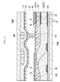
- the display device includes a first substrate SUB1, a wire WI, a first layer LA1 which is an insulation layer, a second layer LA2 which is a color filter CF, a first black matrix BM1, a third layer LA3 which is a flat insulation layer, a fourth layer LA4 which is a first electrode E1, a first alignment layer PI1, a liquid crystal layer LC, a second alignment layer PI2, a second electrode E2, a second black matrix BM2, and a second substrate SUB2, and the layers are sequentially layered.
- the first substrate SUB1, the wire WI, the first layer LA1 which is the insulation layer, the second layer LA2 which is the color filter CF, the first black matrix BM1, the third layer LA3 which is the flat insulation layer, the fourth layer LA4 which is the first electrode E1, the first alignment layer PI1, the liquid crystal layer LC, the second alignment layer PI2, the second electrode E2, the second black matrix BM2, and the second substrate SUB2 may respectively have various structures known to a person skilled in the art, and the structure shown in FIG. 14 is not restrictive.
- one or more surfaces of the first layer LA1 and the second layer LA2 contacting each other and thus forming a first interface corresponding to the first pixel area PX1 are provided as a burned protrusion-depression surface IS
- one or more surfaces of the second layer LA2 and the third layer LA3 contacting each other and thus forming a second interface corresponding to the first pixel area PX1 are provided as a burned protrusion-depression surface IS
- one or more surfaces of the second layer LA2 and the third layer LA3 contacting each other and thus forming a third interface corresponding to the first pixel area PX1 are provided as a burned protrusion-depression surface IS
- one or more surfaces of the third layer LA3 and the fourth layer LA4 contacting each other and thus forming a fourth interface corresponding to the first pixel area PX1 are provided as a burned protrusion-depression surface IS.
- the display device includes a burned black material BE extended to the protrusion-depression surfaces ISs of the second layer LA2 and the third layer LA3 that are disposed facing each other from the first black matrix BM1 disposed neighboring the second interface. That is, at least a part of the black matrix BM extended from the protrusion-depression surfaces ISs may be burned and thus carbonized.
- the first layer LA1 is provided as the insulation layer provided above the first substrate SUB1 and including an inorganic material
- the second layer LA2 is provided as the color filter CF including an organic material
- the third layer LA3 is provided as an insulation layer including an organic material
- the fourth layer LA4 is provided as the first electrode such that surfaces of the second and third layers LA2 and LA3 are respectively provided as protrusion-depression surfaces ISs. Due to the protrusion-depression surfaces ISs, gaps GAs are respectively provided between the first layer LA1 and the second layer LA2, between the second layer LA2 and the third layer LA3, and between the third layer LA3 and the fourth layer LA4.
- the black material BE provided from the first black matrix BM1 fills the gap GA provided between the second layer LA2 and the third layer LA3.
- the lateral surfaces of the second layers LA2 respectively forming the first interface and the second interface, and the lateral surfaces of the third layer LA3 respectively forming the second interface and the third interface are provided as the burned protrusion-depression surfaces ISs, and the gap GA between the second layer LA2 and the third layer LA3 is filled with the burned black material BE. That is, the burned protrusion-depression surface IS corresponding to the first pixel area PX1 and the burned black material BE are viewed dark, and accordingly, the first pixel area PX1 is viewed as a dark spot.
- the lateral surfaces of the second and third layers LA2 and LA3 among the first, second, third, and fourth layers LA1, LA2, LA3, and LA4 that correspond to the first pixel area PX1, which is a defective pixel area, among the first pixel area PX1 and the second pixel area PX2, are provided as the burned protrusion-depression surfaces ISs, and at the same time the burned black material BE is provided corresponding to the first pixel area PX1 so that the defective first pixel area PX1 is viewed as a dark spot, and accordingly, the first pixel area PX1 is prevented from being viewed when other pixels areas among the plurality of pixel areas display an image. That is, a display device in which a first pixel area PX1, which is a defective pixel area, is repaired to be a dark spot by burned protrusion-depression surfaces ISs and the burned black material BE may be provided.
Landscapes
- Physics & Mathematics (AREA)
- Nonlinear Science (AREA)
- Chemical & Material Sciences (AREA)
- Crystallography & Structural Chemistry (AREA)
- General Physics & Mathematics (AREA)
- Optics & Photonics (AREA)
- Mathematical Physics (AREA)
- Engineering & Computer Science (AREA)
- Microelectronics & Electronic Packaging (AREA)
- Devices For Indicating Variable Information By Combining Individual Elements (AREA)
- Electroluminescent Light Sources (AREA)
Abstract
A method for repairing a display device including a defective pixel area (PX1) where a failure has occurred includes irradiating a first laser beam (LB1) to a first interface (IL1) provided between a first layer (LA1, SUB2) and a second layer (LA2, CF) that contact each other corresponding to the defective pixel area (PX1) to form a protrusion-depression surface (IS) in one or more surfaces of the first layer (LA1, SUB2) and the second layer (LA2, CF) that form the first interface (IL1); and irradiating a second laser beam (LB2) to the protrusion-depression surfaces (IS) provided in one or more surfaces of the first and second layers (LA1, SUB2; LA2, CF) to bum the protrusion-depression surface (IS).
Description
- The invention relates generally to a display device and a method for repairing the display device.
- In general, an organic light emitting display, a liquid crystal display ("LCD"), a plasma display panel, and the like are representative examples of a flat panel display.
- The LCD includes a first substrate, a liquid crystal layer, electrodes driving the liquid crystal layer, wires supplying current to the electrodes, a second substrate, and a plurality of insulation layers provided between the first substrate and the second substrate.
- Such an LCD displays predetermined images by forming a plurality of pixel areas, each being the minimum unit for displaying an image, with a first substrate, a liquid crystal layer, electrodes driving the liquid crystal layer, wires supplying current to the electrodes, a second substrate, and a plurality of insulation layers provided between the first substrate and the second substrate.
- When an error occurs in one of the above-stated constituent elements, an error occurs in an image displayed in a defective pixel area where the error occurred among the plurality of pixel areas.
- The invention sets out to provide a display device in which a defective pixel area is repaired, and a method for easily repairing a defective pixel area of a display device.
- One embodiment of the invention provides a method for repairing a display device including a defective pixel area where a failure has occurred. The method include: irradiating a first laser beam to a first interface provided between a first layer and a second layer that contact each other corresponding to the defective pixel area to form a protrusion-depression surface in one or more surfaces of the first layer and the second layer that form the first interface; and irradiating a second laser beam to the protrusion-depression surfaces provided in one or more surfaces of the first and second layers to burn the protrusion-depression surface.
- In an embodiment of the invention, the method further includes flowing a black material melted from a black matrix that neighbors the first interface to the protrusion-depression surface, wherein the irradiating the second laser beam may further include burning the black material provided in the protrusion-depression surface.
- In an embodiment of the invention, the irradiating the first laser beam may further include forming a protrusion-depression surface in one or more surfaces of the second layer and a third layer contacting each other and thus forming a second interface, and, the irradiating the second laser beam may further include burning the protrusion-depression surface provided in one or more surfaces of the second layer and the third layer.
- In an embodiment of the invention, the method may further include flowing a black material melted from a black matrix that is disposed neighboring the second interface to the protrusion-depression surface, and the irradiating the second laser beam may further include burning the black material provided in the protrusion-depression surface.
- In an embodiment of the invention, the irradiating the first laser beam may further include forming a protrusion-depression surface in one or more surfaces of the third layer and a fourth layer that contact each other and thus form a third interface, and the irradiating the second laser beam may further include burning the protrusion-depression surface provided in one or more surfaces of the third layer and the fourth layer.
- Another embodiment of the invention provides a display device including a first pixel area where a failure has occurred and a second pixel area neighboring the first pixel area. The display device includes a first layer and a second layer contacting each other and thus forming a first interface, wherein a burned protrusion-depression surface is provided in one or more surfaces of the first layer and the second layer that form the first interface corresponding to the first pixel area.
- In an embodiment of the invention, the first layer may be a substrate and the second layer may include an organic material.
- In an embodiment of the invention, the second layer may be a color filter.
- In an embodiment of the invention, the protrusion-depression surface may be provided in the second layer.
- In an embodiment of the invention, the first layer may include an inorganic material, and the second layer comprises an organic material.
- In an embodiment of the invention, the protrusion-depression surface may be provided in the second layer.
- In an embodiment of the invention, the display device may further include a black matrix provided neighboring the first interface and extended to the protrusion-depression surface, wherein at least a part of the black matrix extended to the protrusion-depression surface is burned.
- In an embodiment of the invention, the display device may further include a third layer contacting the second layer and thus forming a second interface, wherein a burned protrusion-depression surface may be provided in one or more surfaces of the second and third layers forming the second interface corresponding to the first pixel area.
- In an embodiment of the invention, the second layer and the third layer respectively may include an organic material.
- In an embodiment of the invention, the second layer is may be color filter.
- In an embodiment of the invention, the protrusion-depression surface may be provided in each of the second and third layers.
- In an embodiment of the invention, the second layer may include an organic material, and the third layer may include a transparent conductive oxide.
- In an embodiment of the invention, the protrusion-depression surface may be provided in the second layer.
- In an exemplary embodiment, the display device may further include a black matrix provided neighboring the second interface and extended to the protrusion-depression surface, wherein at least a part of the black matrix extended to the protrusion-depression surface may be burned.
- In an embodiment of the invention, the display device may further include a fourth layer contacting the third layer and thus forming a third interface, wherein a burned protrusion-depression surface may be provided in one or more surfaces of the third and fourth layers forming the third interface corresponding to the first pixel area.
- According to an embodiment of the invention, a display device in which a defective pixel area is repaired and a method for repairing a defective pixel area of the display device can be provided.
- At least some of the above and other features of the invention are set out in the claims.
- The above and other embodiments, advantages and features of this invention will be made more apparent by describing in further detail embodiments thereof with reference to the accompanying drawings, in which:
-
FIG. 1 illustrates a flowchart of an embodiment of a repair method of a display device according to the invention. -
FIG. 2 to FIG. 4 illustrate cross-sectional views of the embodiment of the repair method of the display device according to the invention. -
FIG. 5 illustrates a cross-sectional view of another embodiment of a display device according to the invention. -
FIG. 6 illustrates a flowchart of the other embodiment of a repair method of the display device according to the invention. -
FIGS. 7 and8 illustrate cross-sectional views of the other embodiment of the repair method of the display device according to the invention. -
FIG. 9 illustrates a cross-sectional view of another embodiment of a display device according to the invention. -
FIG. 10 illustrates a cross-sectional view of another embodiment of a display device according to the invention. -
FIG. 11 illustrates a cross-sectional view of another embodiment of a display device according to the invention. -
FIG. 12A illustrates a cross-sectional view of another embodiment of a display device according to the invention. -
FIG. 12B illustrates a cross-sectional view of enlarged portion of the display device ofFIG. 12A ; -
FIG. 13 illustrates a cross-sectional view of another embodiment of a display device according to the invention. -
FIG. 14 illustrates a cross-sectional view of another embodiment of a display device according to the invention. - The invention will be described more fully hereinafter with reference to the accompanying drawings, in which embodiments of the invention are shown. As those skilled in the art would realize, the described embodiments may be modified in various different ways, all without departing from the scope of the invention.
- Accordingly, the drawings and description are to be regarded as illustrative in nature and not restrictive. Like reference numerals designate like elements throughout the specification.
- Further, in embodiments, since like reference numerals designate like elements having the same configuration, a first embodiment is representatively described, and in other embodiments, only configurations that differ from the first embodiment will be described.
- In addition, the size and thickness of each configuration shown in the drawings are arbitrarily shown for better understanding and ease of description, but the invention is not limited thereto.
- In the drawings, the thickness of layers, films, panels, regions, etc., are exaggerated for clarity. In the drawings, for understanding and ease of description, the thickness of some layers and areas is exaggerated. It will be understood that when an element such as a layer, film, region, or substrate is referred to as being "on" another element, it can be directly on the other element or intervening elements may also be present.
- In addition, unless explicitly described to the contrary, the word "comprise" and variations such as "comprises" or "comprising" will be understood to imply the inclusion of stated elements but not the exclusion of any other elements. Further, throughout the specification, the word "on" means positioning on or below the object portion, but does not essentially mean positioning on the upper side of the object portion based on a gravity direction.
- It will be understood that, although the terms "first," "second," "third" etc. may be used herein to describe various elements, components, regions, layers and/or sections, these elements, components, regions, layers and/or sections should not be limited by these terms. These terms are only used to distinguish one element, component, region, layer or section from another element, component, region, layer or section. Thus, "a first element," "component," "region," "layer" or "section" discussed below could be termed a second element, component, region, layer or section without departing from the teachings herein.
- The terminology used herein is for the purpose of describing particular embodiments only and is not intended to be limiting. As used herein, the singular forms "a," "an," and "the" are intended to include the plural forms, including "at least one," unless the content clearly indicates otherwise. "Or" means "and/or." As used herein, the term "and/or" includes any and all combinations of one or more of the associated listed items. It will be further understood that the terms "comprises" and/or "comprising," or "includes" and/or "including" when used in this specification, specify the presence of stated features, regions, integers, steps, operations, elements, and/or components, but do not preclude the presence or addition of one or more other features, regions, integers, steps, operations, elements, components, and/or groups thereof.
- Furthermore, relative terms, such as "lower" or "bottom" and "upper" or "top," may be used herein to describe one element's relationship to another element as illustrated in the Figures. It will be understood that relative terms are intended to encompass different orientations of the device in addition to the orientation depicted in the Figures. For example, if the device in one of the figures is turned over, elements described as being on the "lower" side of other elements would then be oriented on "upper" sides of the other elements. The exemplary term "lower," can therefore, encompasses both an orientation of "lower" and "upper," depending on the particular orientation of the figure. Similarly, if the device in one of the figures is turned over, elements described as "below" or "beneath" other elements would then be oriented "above" the other elements. The exemplary terms "below" or "beneath" can, therefore, encompass both an orientation of above and below.
- "About" or "approximately" as used herein is inclusive of the stated value and means within an acceptable range of deviation for the particular value as determined by one of ordinary skill in the art, considering the measurement in question and the error associated with measurement of the particular quantity (i.e., the limitations of the measurement system). For example, "about" can mean within one or more standard deviations, or within ± 30%, 20%, 10%, 5% of the stated value.
- Unless otherwise defined, all terms (including technical and scientific terms) used herein have the same meaning as commonly understood by one of ordinary skill in the art to which this disclosure belongs. It will be further understood that terms, such as those defined in commonly used dictionaries, should be interpreted as having a meaning that is consistent with their meaning in the context of the relevant art and the present disclosure, and will not be interpreted in an idealized or overly formal sense unless expressly so defined herein.
- Embodiments of the invention are described herein with reference to cross section illustrations that are schematic illustrations of idealized embodiments. As such, variations from the shapes of the illustrations as a result, for example, of manufacturing techniques and/or tolerances, are to be expected. Thus, embodiments described herein should not be construed as limited to the particular shapes of regions as illustrated herein but are to include deviations in shapes that result, for example, from manufacturing. For example, a region illustrated or described as flat may, typically, have rough and/or nonlinear features. Moreover, sharp angles that are illustrated may be rounded. Thus, the regions illustrated in the figures are schematic in nature and their shapes are not intended to illustrate the precise shape of a region and are not intended to limit the scope of the present claims.
- Hereinafter, a repair method of a display device according to an embodiment of the invention will be described with reference to
FIGS. 1 to 4 . -
FIG. 1 illustrates a flowchart of a repair method of a display device according to an embodiment.FIGS. 2 to 4 illustrate cross-sectional views of the repair method of the display device according to the embodiment. - First, as shown in
FIGS. 1 to 3 , a surface having protrusion-depression is formed in an interface by irradiating a first laser beam corresponding to a defective pixel area (S110). - In detail, first, as shown in
FIG. 2 , the display device includes a plurality of pixel areas, each being a minimum unit for displaying an image, and the plurality of pixel areas include a first pixel area PX1 and a second pixel area PX2. The display device includes a first substrate SUB1, a wire WI, a first electrode E1, a first alignment layer PI1, a liquid crystal layer LC, a fourth layer LA4 which is a second alignment layer PI2, a second electrode E2, a third layer LA3 which is an insulation layer, a second layer LA2 which is a color filter CF, a black matrix BM, and a first layer LA1 which is a second substrate SUB2. - The first substrate SUB1, the wiring WI, the first electrode E1, the first alignment layer PI1, the liquid crystal layer LC, the fourth layer LA4 which is the second alignment layer PI2, the second electrode E2, the third layer LA3 which is the insulation layer, the second layer LA2 which is the color filter CF, the black matrix BM, and the first layer LA1 which is the second substrate SUB2 may have various structures known to a person skilled in the art, and thus the structure shown in
FIG. 2 is not restrictive. - In order to determine whether an error has occurred in the plurality of pixel areas of the display device, a lighting test is performed, and when it is determined that an error has occurred in a first pixel area PX1 among the first pixel area PX1 and the second pixel area PX2 of the plurality of pixel areas, the first laser beam LB1 is irradiated to a first interface IL1 between the first layer LA1 which is the second substrate SUB2 and the second layer LA2 which is the color filter CF. Here, the first layer LA1 and the second layer LA2 contact each other corresponding to the first pixel area PX1 which is the defective pixel area. The first laser beam LB1 may scan the entire area of the first pixel area PX1 with various routes in a plane.
- As shown in
FIGS. 2 and3 , the first laser beam LB1 may be irradiated to one of the first interface IL1 between the first layer LA1 and the second layer LA2 that contact each other, a second interface IL2 between the second layer LA2 and the third layer LA3 that contact each other, and a third interface IL3 between the third layer LA3 and the fourth layer LA4 that contact each other, and a surface of one of layers including an organic material among the first, second, third, and fourth layers LA1, LA2, LA3, and LA4 is formed as a surface IS having protrusion-depression caused by energy from the first laser beam LB1. That is, one or more surfaces of the first layer LA1 and the second layer LA2 forming the first interface IL1 between the first layer LA1 and the second layer LA2 that contact each other is formed as the surface IS having protrusion-depression, one or more surfaces of the second layer LA2 and the third layer LA3 forming the second interface IL2 between the second layer LA2 and the third layer LA3 that contact each other is formed as the surface IS having protrusion-depression, and one or more surfaces of the third layer LA3 and the fourth layer LA4 forming the third interface IL3 between the third layer LA3 and the fourth layer LA4 that contact each other is formed as the surface IS having protrusion-depression. - In an embodiment of the invention, when the first laser beam LB1 is irradiated to the second interface IL2, the energy from the first laser beam LB1 is transferred not only to the first interface IL1 but also to the third interface IL3 that neighbors the second interface IL2 while at the same time the first laser beam LB1 passes through the first interface IL1 such that a surface of one or more layers including an organic material among the first, second, third, and fourth layers LA1, LA2, LA3, and LA4 is provided as the surface IS having protrusion-depression, for example.
- In this embodiment, the first layer LA1 includes the second substrate SUB2 that may include an inorganic material, metal, and glass, the second layer LA2 includes the color filter CF including an organic material, the third layer LA3 includes an insulation layer including an organic material, and the fourth layer LA4 includes the second alignment layer PI2 including an organic material such that the surface of each of the second, third, and fourth layers LA2, LA3, and LS4 is provided as the surface IS having the protrusion-depression by the first laser beam LB1. Gaps GA are respectively defined between the first interface IL1, the second interface IL2, and the third interface IL3 where the surfaces IS having protrusion-depression are provided. Specifically, lateral surfaces of the second layer LA2 where the first interface IL1 and the second interface IL2 are provided are provided as the surfaces IS having protrusion-depression, lateral surfaces of the third layer LA3 where the second interface IL2 and the third interface IL3 are provided are provided as the surfaces IS having protrusion-depression, and one surface of the fourth layer LA4 where the third interface IL3 is provided is provided as the surface IS having protrusion-depression.
- Next, as shown in
FIG. 4 , the surface IS having protrusion-depression is burnt by irradiating a second laser beam LB2 thereto (S120 inFIG. 1 ). - Specifically, the second laser beam LB2 is irradiated to one or more surfaces IS having protrusion-depression among the first layer LA1 and the second layer LA2 corresponding to the first pixel area PX1, which is a defective pixel area, so as to burn the surface IS having protrusion-depression. The surface IS having protrusion-depression may be carbonized while being burnt by irradiation of the second laser beam LB2, and accordingly, the first pixel area PX1, which is the defective pixel area, may be recognized as a dark spot.
- The second laser beam LB2 may scan the entire area of the first pixel area PX1 with various routes in a plane.
- The second laser beam LB2 may be irradiated to one or more surfaces IS having protrusion-depression among the first layer LA1, the second layer LA2, the third layer LA3, and the fourth layer LA4, and the protrusion-depression surface IS provided in the surface of one or more layers of the second layer LA2, the third layer LA3, and the fourth layer LA4 including an organic material may be carbonized while being burnt by energy of the second laser beam LB2. That is, the protrusion-depression surface IS provided in one or more surfaces of the first layer LA1 and the second layer LA2 is burnt by the second laser beam LB2, the protrusion-depression surface IS provided in one or more surfaces of the second layer LA2 and the third layer LA3 is burnt, and the protrusion-depression surface IS provided in one or more surfaces of the third layer LA3 and the fourth layer LA4 is burnt, and accordingly each protrusion-depression surface IS may be carbonized.
- In an exemplary embodiment, when the second laser beam LB2 is irradiated to the protrusion-depression surface IS of the third layer LA3, the second laser beam LB2 passes the protrusion-depression surface IS of one or more of the first layer LA1 and the second layer LA2 and at the same time the energy from the second laser beam LB2 is transferred to the protrusion-depression surface IS of the fourth layer LA4 that neighbors the third layer LA3 such that one or more protrusion-depression surfaces IS including an organic material among the first layer LA1, the second layer LA2, the third layer LA3, and the fourth layer LA4 may be burnt and thus carbonized by the energy of the second laser beam LB2, for example. The protrusion-depression surface IS occupies much more surface area compared to a flat surface in the same space, and thus the protrusion-depression surface IS may be easily carbonized by being burnt by the energy of the second laser beam LB2.
- In this embodiment, the protrusion-depression surface IS is provided in each of the second layer LA2, the third layer LA3, and the fourth layer LA4, and the respective protrusion-depression surfaces IS may be burnt and then carbonized by the energy of the second laser beam LB2. Specifically, the protrusion-depression surfaces IS provided in lateral sides of the second layer LA2, the protrusion-depression surfaces IS provided in lateral sides of the third layer LA3, and the protrusion-depression surface IS provided in one side of the fourth layer LA4 may be respectively burnt and then carbonized by the second laser beam LB2.
- As described, according to the repair method of the display device of this embodiment of the invention, the surfaces of the second layer LA2, the third layer LA3, and the fourth layer LA4 among the first layer LA1, the second layer LA2, the third layer LA3, and the fourth layer LA4 that correspond to the first pixel area PX1, which is a defective pixel area, among the first pixel area PX1 and the second pixel area pX2 of the display device are respectively provided as the protrusion-depression surfaces IS, and the protrusion-depression surfaces IS are burnt to be carbonized such that the first pixel area PX1, which is the defective pixel area, is recognized as a dark spot, thereby preventing the first pixel area PX1 from being viewed. That is, according to the repair method of the display device, a defective pixel area may be repaired by irradiation of a laser beam twice.
- In the illustrated embodiments of the invention, a liquid crystal display ("LCD") will be described as a display device using the above-state repairing method, but the invention is not so limited. A repairing method of a display device according to another exemplary embodiment may be used in various display devices such as an organic light emitting diode display ("OLED"), plasma displays ("PDs"), field emission displays ("FEDs"), electrophoretic displays ("EPDs"), electrowetting displays ("EWDs"), and the like as long as one or more layers among two layers contacting each other and thus forming an interface include an organic material.
- Hereinafter, a display device according to another embodiment of the invention will be described with reference to
FIG. 5 . - A display device to be described hereinafter according to another embodiment of the invention may be a display device repaired by the above-described repair method of the display device.
-
FIG. 5 illustrates a cross-sectional view of a display device according to another embodiment of the invention. - As shown in
FIG. 5 , a display device according to another embodiment includes a plurality of pixel areas, each being a minimum unit for displaying an image, and the plurality of pixel areas include a first pixel area PX1, which is a defective pixel area where an error has occurred, and a second pixel area PX2, which is a normal pixel area where no error has occurred. The display device includes a first substrate SUB1, a wire WI, a first electrode E1, a first alignment layer PI1, a liquid crystal layer LC, a fourth layer LA4 which is a second alignment layer PI2, a second electrode E2, a third layer LA3 which is an insulation layer, a second layer LA2 which is a color filter CF, a black matrix BM, and a first layer LA1 which is a second substrate SUB2, and they are sequentially layered. - The first substrate SUB1, the wire WI, the first electrode E1, the first alignment layer PI1, the liquid crystal layer LC, the fourth layer LA4 which is the second alignment layer PI2, the second electrode E2, the third layer LA3 which is the insulation layer, the second layer LA2 which is the color filter CF, the black matrix BM, and the first layer LA1 which is the second substrate SUB2 may have various structures known to a person skilled in the art, and thus the structure shown in
FIG. 5 is not restrictive. - In the display device according to this embodiment of the invention, one or more surfaces of the first and second layers LA1 and LA2 being in contact with each other and thus forming a first interface are provided as a burned protrusion-depression surface IS corresponding to the first pixel area PX1, one or more surfaces of the second and third layers LA2 and LA3 being in contact with each other and thus forming a second interface are provided as a burned protrusion-depression surface IS corresponding to the first pixel area PX1, and one or more surfaces of the third and fourth layers LA3 and LA4 being in contact with each other and thus forming a third interface are provided as a burned protrusion-depression surface IS corresponding to the first pixel area PX1.
- In a display device according to this embodiment of the invention, the first layer LA1 is provided as a second substrate SUB2 that may include an inorganic material, a metal, glass, and the like, the second layer LA2 is provided as a color filter CF including an organic material, the third layer LA3 is provided as an insulation layer including an organic material, and the fourth layer LA4 is provided as a second alignment layer PI2 including an organic material such that a surface of each of the second, third, and fourth layers LA2, LA3, and LA4 is provided as a burned protrusion-depression surface IS. The protrusion-depression surfaces IS of the first, second, third, and fourth layers LA1, LA2, LA3, and LA4 define gaps GA between the first and second layers LA1 and LA2, between the second and third layers LA2 and LA3, and between the third and fourth layers LA3 and LA4, respectively. Specifically, lateral surfaces of the second layer LA2 respectively forming the first interface and the second interface are provided as the burned protrusion-depression surfaces IS, lateral surfaces of the third layer LA3 respectively forming the second interface and the third interface are provided as the burned protrusion-depression surfaces IS, and one surface of the fourth layer LA4 forming the third interface is provided as the burned protrusion-depression surface IS. That is, the protrusion-depression surfaces IS burned corresponding to the first pixel area PX1 are viewed as dark, and accordingly, the first pixel area PX1 is viewed as a dark spot.
- As described, in the display device according to this embodiment, surfaces of the second, third, and fourth layers LA2, LA3, and LA4 among the first layer LA1, the second layer LA2, the third layer LA3, and the fourth layer LA4 that correspond to the first pixel area PX1, which is a defective pixel area where a failure has occurred among the first pixel area PX1 and the second pixel area PX2, are respectively provided as the burned protrusion-depression surfaces IS so that the first pixel area PX1, which is a defective pixel area, is viewed as a dark spot, and thus the first pixel area PX1 may be prevented from being viewed when other pixel areas among the plurality of pixel areas display an image. That is, a display device of which the first pixel area PX1, which is a defective pixel area, is repaired to be a dark spot by the burned protrusion-depression surface IS may be provided.
- The display device according to this embodiment of the invention is exemplarily described as an LCD, but any display device of which one or more layers among two layers forming an interface by being in contact with each other includes an organic material is applicable. In an exemplary embodiment, OLED, PDs, FEDs, EPDs, and EWDs are applicable, for example.
- Hereinafter, a display device according to another embodiment of the invention will be described with reference to
FIG. 6 to FIG. 8 . -
FIG. 6 is a flowchart illustrating a repairing method of a display device according to another embodiment of the invention.FIGS. 7 and8 illustrate cross-sectional views provided for description of the repairing method of the display device according to the other embodiment of the invention. - First, as shown in
FIGS. 6 and7 , a first laser beam is irradiated to an interface corresponding to a defective pixel area to form a protrusion-depression surface (S210). - Specifically, as shown in
FIG. 7 , the display device includes a plurality of pixel areas, each being the minimum unit for displaying an image, and the plurality of pixel areas include a first pixel area PX1 and a second pixel area PX2. The display device includes a first substrate SUB1, a wire WI, a first electrode E1, a first alignment layer PI1, a liquid crystal layer LC, a fourth layer LA4 which is a second alignment layer PI2, a third layer LA3 which is an insulation layer, a second layer LA2 which is a color filter CF, a black matrix BM, and a first layer LA1 which is a second substrate SUB2. - The first substrate SUB1, the wire WI, the first electrode E1, the first alignment layer PI1, the liquid crystal layer LC, the fourth layer LA4 which is the second alignment layer PI2, the second electrode E2, the third layer LA3 which is the insulation layer, the second layer LA2 which is the color filter CF, the black matrix BM, and the first layer LA which is the second substrate SUB2, may have various structures known to a person skilled in the art, and thus the structure shown in
FIG. 7 is not restrictive. - In order to determine whether the plurality of pixel areas included in the display device are defective, a lighting test is performed, and when it is determined that the first pixel area PX1 among the first and second pixel areas PX1 and PX2 of the plurality of pixel areas is a defective pixel area, a first laser beam is irradiated to a first interface between the first layer LA1, which is the second substrate SUB2, and the second layer LA2, which is the color filter CF, being in contact each other corresponding to the defective first pixel area PX1. The first laser beam may scan the entire area of the first pixel area PX1 with various routes in a plane.
- The first laser beam may be irradiated to one or more interfaces among the first interface between the first layer LA1 and the second layer LA2 contacting each other, a second interface between the second layer LA2 and the third layer LA3 contacting each other, and a third interface between the third layer LA3 and the fourth layer LA4 contacting each other, and a surface of one or more layers including an organic material among the first, second, third, and fourth layers LA1, LA2, LA3, and LA4 is provided as a protrusion-depression surface IS. That is, one or more surfaces among the first layer LA1 and the second layer LA2 contacting each other and thus forming the first interface is provided as a protrusion-depression surface IS by the first laser beam, one or more surfaces among the second layer LA2 and the third layer LA3 contacting each other and thus forming the second interface is provided as a protrusion-depression surface IS by the first laser beam, and one or more surfaces among the third layer LA3 and the fourth layer LA4 contacting each other and thus forming the third interface is provided as a protrusion-depression surface IS by the first laser beam.
- In an embodiment of the invention, when the first laser beam is irradiated to the second interface, the first laser beam passes the first interface and at the same time energy of the first laser beam is transmitted to the third interface that neighbors the second interface so that a surface of one or more layers including an organic material among the first, second, third, and fourth layers LA1, LA2, LA3, and LA4 is provided as a protrusion-depression surface IS, for example.
- In another embodiment of the invention, the first layer LA1 is provided as a second substrate SUB2 that may include an inorganic material, a metal, and glass, the second layer LA2 is provided as a color filter CF including an organic material, the third layer LA3 is provided as an insulation layer including an organic material, and the fourth layer LA4 is provided as a second alignment layer PI2 including an organic material so that a surface of each of the second, third, and fourth layers LA2, LA3, and LA4 is provided as a protrusion-depression surface IS by the first laser beam. The protrusion-depression surfaces ISs provided in the first interface, the second interface, and the third interface respectively define gaps GA. Specifically, lateral surfaces of the second layer LA2, respectively forming the first interface and the second interface are provided as the protrusion-depression surfaces ISs, lateral surfaces of the third layer LA3, respectively forming the second interface and the third interface are provided as the protrusion-depression surfaces IS, and one surface of the fourth layer LA4, forming the third interface is provided as the protrusion-depression surface IS.
- Next, as shown in
FIG. 8 , a black material formed by melting the black matrix flows to the protrusion-depression surface (S220). - In an embodiment of the invention, the black matrix BM that neighbors the first interface is melted by using ultraviolet ("UV") rays, a laser beam, or heat, and a black material BE provided by melting the black matrix BM flows through the gap GA defined between the first layer LA1 and the second layer LA2 along the protrusion-depression surface IS of the second layer LA2. Thus, the surface of the protrusion-depression surface IS of the second layer LA2 is covered by the black material BE, and the gap GA defined between the first layer LA1 and the second layer LA2 is filled with the black material BE.
- In another embodiment of the invention, when the black matrix BM neighbors the second interface disposed between the second layer LA2 and the third layer LA3, a black material BE provided by melting the black matrix BM that neighbors the second interface may flow to each protrusion-depression surface IS of the second layer LA2 and the third layer LA3 that face opposite to each other.
- Next, a second laser beam is irradiated to the protrusion-depression surfaces to burn the protrusions and depression surfaces and the black material (S230).
- Specifically, the second laser beam LB2 is irradiated to the protrusion-depression surface IS provided in one or more surfaces among the first layer LA1 and the second layer LA2 corresponding to the first pixel area PX1, which is a defective pixel area, to burn the protrusion-depression surface IS and the black material BE in the protrusion-depression surface IS. The protrusion-depression surface IS and the black material BE2 may be carbonized while being burned by the second laser beam LB2, and accordingly the first pixel area PX1, which is a defective pixel area, may be viewed as a dark spot.
- In another embodiment of the invention, when the black matrix is located neighboring the second interface where the second layer LA2 and the third layer LA3 contact each other, the black material provided by melting the black matrix in the protrusion-depression surfaces ISs of the second and third layers LA2 and LA3 that face opposite to each other may be burned.
- The second laser beam LB2 may scan the entire area of the first pixel area PX1 with various routes in a plane.
- The second laser beam LB2 may be irradiated to one or more protrusion-depression surfaces ISs among the first, second, third, and fourth layers LA1, LA2, LA3, and LA4, and the protrusion-depression surface IS and the black material BE in the protrusion-depression surface IS provided in one or more layers among the second layer LA2, the third layer LA3, and the fourth layer LA4, including an organic material may be carbonized while being burned by the energy of the second laser beam LB2. That is, the protrusion-depression surface IS provided in one or more surfaces of the first and second layers LA1 and LA2 is burned by the second laser beam LB2, the protrusion-depression surface IS provided in one or more surfaces of the second and third layer LA2 and LA3 is burned by the second laser beam LB2, and the black materials BE in the protrusion-depression surfaces ISs are burned such that the respective protrusion-depression surface ISs and the black materials BE may be carbonized.
- In an embodiment of the invention, when the second laser beam LB2 is irradiated to the protrusion-depression surface IS of the third layer LA3, the second laser beam LB2 passes one or more protrusion-depression surfaces IS of the first and second layers LA1 and LA2 and at the same time energy of the second laser beam LB2 is transmitted to the protrusion-depression surface IS of the fourth layer LA4 that neighbors the third layer LA3 so that one or more protrusions and depression surfaces ISs, including the organic material among the first, second, third, and fourth layers LA1, LA2, LA3, and LA4 and the black material BE in the protrusion-depression surface IS of the second layer LA2 may be burned and thus carbonized, for example. Since the protrusion-depression surface IS has a larger surface area compared to those of other flat surfaces in the same predetermined space, the protrusion-depression surface IS may be easily burned and thus carbonized by energy of the second laser beam LB2. In addition, the black material BE has high energy absorption capability, and thus the black material BE may be easily burned and thus carbonized by energy of the second laser beam LB2.
- In another embodiment of the invention, the protrusion-depression surface IS may be provided in each of the second, third, and fourth layers LA2, LA3, and LA4, and the black material BE is provided in the second layer LA2 so that the protrusion-depression surfaces ISs of the first, second, third, and fourth layers LA1, LA2, LA3, and LA4 and the black material BE may be respectively burned and thus carbonized by the second laser beam LB2. Specifically, the protrusion-depression surfaces ISs provided in lateral surfaces of the second layer LA2, the protrusion-depression surface IS provided in one surface of the fourth layer LA4, and the black material provided in the protrusion-depression surfaces ISs of the second layer LA2 may be burned and thus carbonized by the second laser beam LB2.
- As described, the surface of each of the first, second, third, and fourth layers LA1, LA2, LA3, and LA4 that correspond to the first pixel area PX1, which is a defective pixel area where a failure has occurred among the first pixel area PX1 and the second pixel area PX2 of the display device, is provided as a protrusions and depression surface IS, and at the same time the black material is located on the protrusion-depression surface IS of the second layer LA2, and the protrusion-depression surface IS and the black material BE are burned to be carbonized such that the first pixel area PX1, which is a defective pixel area, is treated as a dark spot to thereby suppress the first pixel area PX1 from being viewed by using the repair method of the display device according to the illustrated exemplary embodiment. That is, laser beams are irradiated two times to easily repair a defective pixel area according to the repair method of the display device.
- Hereinafter, a display device according to another embodiment of the invention will be described with reference to
FIG. 9 . - A display device according to another embodiment of the invention, which will be described hereinafter, may be a display device repaired by using the repair method of the display device according to another embodiment of the invention.
-
FIG. 9 illustrates a cross-sectional view of a display device according to another embodiment of the invention. - As shown in
FIG. 9 , a display device according to another embodiment of the invention includes a plurality of pixel areas, each being the minimum unit for displaying an image, and the plurality of pixel areas include a first pixel area PX1, which is a defective pixel area where a failure has occurred, and a second pixel area PX2, which is a normal pixel area where no failure has occurred. The display device includes a first substrate SUB1, a wire WI, a first electrode E1, a first alignment layer PI1, a liquid crystal layer LC, a fourth layer LA4, which is a second alignment layer PI2, a second electrode E2, a third layer LA3 which is an insulation layer, a second layer LA2 which is a color filter CF, a black matrix BM, and a first layer LA1 which is a second substrate SUB2, and the layers are sequentially layered. - The first substrate SUB1, the wire WI, the first electrode E1, the first alignment layer PI1, the liquid crystal layer LC, the fourth layer LA4 which is the second alignment layer PI2, the second electrode E2, the third layer LA3 which is the insulation layer, the second layer LA2 which is the color filter CF, the black matric BM, and the first layer LA1 which is the second substrate SUB2 may have various structures known to a person skilled in the art, and thus the structure shown in
FIG. 9 is not restrictive. - In the display device according to the embodiment of the invention, one or more surfaces of the first layer LA1 and the second layer LA2 contacting each other and thus forming a first interface corresponding to the first pixel area PX1 are provided as a burned protrusion-depression surface IS, one or more surfaces of the second layer LA2 and the third layer LA3 contacting each other and thus forming a second interface corresponding to the first pixel area PX1 are provided as a burned protrusion-depression surface IS, one or more surfaces of the second layer LA2 and the third layer LA3 contacting each other and thus forming a third interface corresponding to the first pixel area PX1 are provided as a burned protrusion-depression surface IS, and one or more surfaces of the third layer LA3 and the fourth layer LA4 contacting each other and thus forming a fourth interface corresponding to the first pixel area PX1 are provided as a burned protrusion-depression surface IS. Further, the display device includes a burned black material BE extended from the black matrix BM located neighboring the first interface to the protrusion-depression surface IS of the second layer LA2. That is, at least a part of the black matrix BM extended to the protrusion-depression surface IS may be burned and thus carbonized.
- In the display device according to the illustrated embodiment of the invention, the first layer LA1 is provided as the second substrate SUB2 that may include an inorganic material, a metal, and glass, the second layer LA2 is provided as the color filter including an organic material, the third layer LA3 is provided as the insulation layer including an organic material, and the fourth layer LA4 is provided as the second alignment layer PI2 including an organic material such that the surface of each of the second, third, and fourth layers LA2, LA3, and LA4 is provided as a burned protrusion-depression surface IS. Gaps GA are defined respectively between the first layer LA1 and the second layer LA2, between the second layer LA2 and the third layer LA3, and between the third layer LA3 and the fourth layer LA4. Here, the gap GA defined between the first layer LA1 and the second layer LA2 is filled with the black material BE provided from the black matrix BM. Specifically, lateral surfaces of the second layer LA2 respectively forming the first interface and the second interface are provided as burned protrusion-depression surfaces ISs, lateral surfaces of the third layer LA3 respectively forming the second interface and the third interface are provided as burned protrusion-depression surfaces ISs, one surface of the fourth layer LA4 forming the third interface is provided as a burned protrusion-depression surface IS, and the gap GA between the first layer LA1 and the second layer LA2 is filled with the burned black material BE. That is, the burned protrusion-depression surfaces IS and the burned black material BE corresponding to the first pixel area PX1 are viewed dark, and accordingly, the first pixel area PX1 is viewed as a dark spot.
- As described, in the display device according to the illustrated embodiment of the invention, the surfaces of the second, third, and fourth layers LA2, LA3, and LA4 among the first, second, third, and fourth layers LA1, LA2, LA3, and LA4 that correspond to the first pixel area PX1, which is a defective pixel area, among the first pixel area PX1 and the second pixel area PX2 are provided as the burned protrusion-depression surfaces ISs and at the same time the burned black material BE is provided corresponding to the first pixel area PX1 so that the defective first pixel area PX1 is viewed as a dark spot, and accordingly the first pixel area PX1 is prevented from being viewed when other pixels areas among the plurality of pixel areas display an image. That is, the display device according to the illustrated exemplary embodiment repairs the first pixel area PX1, which is a defective pixel area, to be a dark spot by the burned protrusion-depression surfaces ISs and the burned black material BE.
- Hereinafter, a display device according to another embodiment of the invention will be described with reference to
FIG. 10 . The display device may be a display device repaired by using a repair method of a display device according to another embodiment of the invention. -
FIG. 10 illustrates a cross-sectional view of a display device according to another embodiment of the invention. - As shown in
FIG. 10 , a display device according to this embodiment includes a plurality of pixel areas, each being the minimum unit for displaying an image, and the plurality of pixel areas include a first pixel area PX1 which is a defective pixel area where a failure has occurred, and a second pixel area PX2 which is a normal pixel area where no failure has occurred. The display device includes a first substrate SUB1, a wire WI, a color filter CF, a first electrode E1, a first alignment layer PI1, a liquid crystal layer LC, a second alignment layer PI2, a third layer LA3 which is a second electrode E2, a second layer LA2 which is an insulation layer, a black matrix BM, and a first layer LA1 which is a second substrate SUB2, and the layers are sequentially layered. - The display device includes the first substrate SUB1, the wire WI, the color filter CF, the first electrode E1, the first alignment layer PI1, the liquid crystal layer LC, the second alignment layer PI2, the third layer LA3 which is the second electrode E2, the second layer LA2 which is the insulation layer, the black matrix BM, and the first layer LA1 which is the second substrate SUB2 may respectively have various structures known to a person skilled in the art, and thus the structure shown in
FIG. 10 is not restrictive. - In the display device according to this embodiment of the invention, one or more surfaces of the first layer LA1 and the second layer LA2 contacting each other and thus forming a first interface corresponding to the first pixel area PX1 are provided as a burned protrusion-depression surface IS, and one or more surfaces of the second layer LA2 and the third layer LA3 contacting each other and thus forming a second interface corresponding to the first pixel area PX1 are provided as a burned protrusion-depression surface IS.
- In the display device according to this embodiment of the invention, the first layer LA1 is provided as the second substrate SUB2 that may include an inorganic material, a metal, and glass, the second layer LA2 is provided as the insulation layer that includes an organic material, and the third layer LA3 is provided as a transparent conductive oxide including indium tin oxide ("ITO") or indium zinc oxide ("IZO") such that lateral surfaces of the second layer LA2 are provided as burned protrusion-depression surfaces ISs. Due to the protrusion-depression surfaces ISs, gaps Gas are respectively defined between the first layer LA1 and the second layer LA2 and between the second layer LA2 and the third layer LA3. Specifically, lateral surfaces of the second layer LA2, respectively forming the first interface and the second interface are provided as the burned protrusion-depression surfaces ISs. That is, the protrusion-depression surfaces ISs burned corresponding to the first pixel area PX1 are viewed dark, and thus the first pixel area PX1 is viewed as a dark spot.
- As described, in the display device according to this embodiment of the invention, the lateral surfaces of the second layer LA2 among the first, second, and third layers LA1, LA2, and LA3 corresponding to the first pixel area PX1 which is a defective pixel area among the first pixel area PX1 and the second pixel area PX2 are provided as the burned protrusion-depression surfaces ISs and thus the defective first pixel area PX1 is viewed as a dark spot, and accordingly, the first pixel area PX1 may be prevented from being viewed when other pixel areas of the plurality of pixel areas display an image. That is, a display device in which a first pixel area PX1, which is a defective pixel area, is repaired to be a dark spot by burned protrusion-depression surfaces ISs may be provided.
- Hereinafter, a display device according to another embodiment of the invention will be described with reference to
FIG. 11 . The display device may be a display device repaired by using a repair method of a display device according to another embodiment of the invention. -
FIG. 11 illustrates a cross-sectional view of a display device according to another embodiment of the invention. - As shown in
FIG. 11 , a display device according to this embodiment includes a plurality of pixel areas, each being the minimum unit for displaying an image, and the plurality of pixel areas include a first pixel area PX1, which is a defective pixel area where a failure has occurred, and a second pixel area PX2, which is a normal pixel area where no failure has occurred. The display device includes a first substrate SUB1, a wire WI, a color filter CF, a first electrode E1, a first alignment layer PI1, a liquid crystal layer LC, a second alignment layer PI2, a third layer LA3 which is a second electrode E2, a second layer LA2 which is an insulation layer, a black matrix BM, and a first layer LA1 which is a second substrate SUB2, and the layers are sequentially layered. - The first substrate SUB1, the wire WI, the color filter CF, the first electrode E1, the first alignment layer PI1, the liquid crystal layer LC, the second alignment layer PI2, the third layer LA3 which is the second electrode E2, the second layer LA2 which is the insulation layer, the black matrix BM, and the first layer LA1 which is the second substrate SUB2 may respectively have various structures, and thus the structure shown in
FIG. 11 is not restrictive. - In the display device according to this embodiment of the invention, one or more surfaces of the first layer LA1 and the second layer LA2 contacting each other and thus forming a first interface corresponding to the first pixel area PX1 are provided as a burned protrusion-depression surface IS, and one or more surfaces of the second layer LA2 and the third layer LA3 contacting each other and thus forming a third interface corresponding to the first pixel area PX1 are provided as a burned protrusion-depression surface IS. Further, the display device includes a burned black material BE extended from the black matrix BM disposed neighboring the first interface to the protrusion-depression surfaces ISs of the second layer LA2. That is, at least a part of the black matrix BM extended to the protrusion-depression surface IS may be burned and thus carbonized.
- In a display device according to the illustrated embodiment of the invention, the first layer LA1 is provided as the second substrate SUB2 that may include an inorganic material, a metal, and glass, the second layer LA2 is provided as the insulation layer including an organic material, and the third layer LA3 is provided as a transparent conductive oxide including ITO or IZO so that lateral surfaces of the second layer LA2 are provided as burned protrusion-depression surfaces ISs. Due to the protrusion-depression surfaces ISs, gaps Gas are respectively defined between the first layer LA1 and the second layer LA2 and between the second layer LA2 and the third layer LA3. Here, the black material BE provided from the black matrix BM fills the gap GA defined between the first layer LA1 and the second layer LA2. Specifically, the lateral surfaces of the second layers LA2 respectively forming the first interface and the second interface are provided as the burned protrusion-depression surfaces ISs, and the gap GA between the first layer LA1 and the second layer LA2 is filled with the burned black material BE. That is, the burned protrusion-depression surface IS corresponding to the first pixel area PX1 and the burned black material BE are viewed dark, and accordingly, the first pixel area PX1 is viewed as a dark spot.
- As described, in a display device according to the illustrated embodiment of the invention, the lateral surfaces of the second layer LA2 among the first, second, and third layers LA1, LA2, and LA3 corresponding to the first pixel area PX1, which is a defective pixel area among the first pixel area PX1 and the second pixel area PX2, are provided as the burned protrusion-depression surfaces ISs, and simultaneously the burned black material BE is provided corresponding to the first pixel area PX1 so that the first pixel area PX1 which is the defective pixel area is viewed as a dark spot, and accordingly, the first pixel area PX1 may be prevented from being viewed when other pixel areas among the plurality of pixel areas display an image. That is, a display device in which a first pixel area PX1, which is a defective pixel area, is repaired to be a dark spot by burned protrusion-depression surfaces ISs and the burned black material BE may be provided.
- Hereinafter, a display device according to another embodiment of the invention will be described with reference to
FIGS. 12A and12B . The display device may be a display device repaired by using a repair method of a display device according to another embodiment of the invention. -
FIGS. 12A and12B illustrate a cross-sectional view of a display device according to another embodiment of the invention and an enlarged view of a portion of the display device. - As shown in
FIGS. 12A and12B , a display device according to this embodiment includes a plurality of pixel areas, each being the minimum unit for displaying an image, and the plurality of pixel areas include a first pixel area PX1 which is a defective pixel area where a failure has occurred, and a second pixel area PX2 which is a normal pixel area where no failure has occurred. The display device includes a first layer SUB1, a wire WI, a first layer LA1 which is an insulation layer, a second layer LA2 which is a color filter CF, a third layer LA3 which is an insulation layer, a fourth layer LA4 which is a first electrode E1, a first alignment layer PI1, a liquid crystal layer LC, a second alignment layer PI2, a second electrode E2, a black matrix BM, and a second substrate SUB2, and the layers are sequentially layered. - The first substrate SUB1, the wire WI, the first layer LA1 which is the insulation layer, the second layer LA2 which is the color filter CF, the third layer LA3 which is the insulation layer, the fourth layer LA4 which is the first electrode E1, the first alignment layer PI1, the liquid crystal layer LC, the second alignment layer PI2, the second electrode E2, the black matrix BM, and the second substrate SUB2 may respectively have various structures known to a person skilled in the art, and thus the structure shown in
FIGS. 12A and12B is not restrictive. - In the display device according to the illustrated embodiment of the invention, one or more surfaces of the first layer LA1 and the second layer LA2 contacting each other and thus forming a first interface corresponding to the first pixel area PX1 are provided as a burned protrusion-depression surface IS, one or more surfaces of the second layer LA2 and the third layer LA3 contacting each other and thus forming a second interface corresponding to the first pixel area PX1 are provided as a burned protrusion-depression surface IS, one or more surfaces of the second layer LA2 and the third layer LA3 contacting each other and thus forming a third interface corresponding to the first pixel area PX1 are provided as a burned protrusion-depression surface IS, and one or more surfaces of the third layer LA3 and the fourth layer LA4 contacting each other, and thus forming a fourth interface corresponding to the first pixel area PX1 are provided as a burned protrusion-depression surface IS.
- In the display device according to the illustrated embodiment of the invention, the first layer LA1 is provided as the insulation layer provided above the first substrate SUB1 and including an inorganic material, the second layer LA2 is provided as the color filter CF including an organic material, the third layer LA3 is provided as an insulation layer including an organic material, and the fourth layer LA4 is provided as the first electrode such that surfaces of the second and third layers LA2 and LA3 are respectively provided as protrusion-depression surfaces ISs. Due to the protrusion-depression surfaces ISs, gaps GAs are respectively defined between the first layer LA1 and the second layer LA2, between the second layer LA2 and the third layer LA3, and between the third layer LA3 and the fourth layer LA4. Specifically, the lateral surfaces of the second layer LA2, respectively forming the first interface and the second interface, are provided as burned protrusion-depression surfaces ISs, and the lateral surfaces of the third layer LA3, respectively forming the second interface and the third interface, are provided as burned protrusion-depression surfaces ISs. That is, the burned protrusion-depression surfaces IS are viewed dark, and accordingly, the first pixel area PX1 is viewed as a dark spot.
- As described, in the display device according to the exemplary embodiment, the lateral surfaces of the second and third layers LA2 and LA3 among the first, second, third, and fourth layers LA1, LA2, LA3, and LA4 that correspond to the first pixel area PX1 which is a defective pixel area, among the first pixel area PX1 and the second pixel area PX2, are provided as the burned protrusion-depression surfaces ISs so that the defective first pixel area PX1 is viewed as a dark spot, and accordingly, the first pixel area PX1 is prevented from being viewed when other pixels areas among the plurality of pixel areas display an image. That is, a display device in which a first pixel area PX1, which is a defective pixel area, is repaired to be a dark spot by burned protrusion-depression surfaces ISs may be provided.
- Hereinafter, a display device according to another embodiment of the invention will be descried with reference to
FIG. 13 . The display device may be a display device repaired by using a repair method of a display device according to another embodiment of the invention. -
FIG. 13 illustrates a cross-sectional view of a display device according to another embodiment of the invention. - As shown in
FIG. 13 , a display device according to this embodiment of the invention includes a plurality of pixel areas, each being the minimum unit for displaying an image, and the plurality of pixel areas include a first pixel area PX1 which is a defective pixel area where a failure has occurred, and a second pixel area PX2 which is a normal pixel area where no failure has occurred. The display device includes a first substrate SUB1, a wire WI, a first layer LA1 which is an insulation layer, a second layer LA2 which is a color filter CF, a third layer LA3 which is a flat insulation layer, a fourth layer LA4 which is a first electrode E1, a first alignment layer PI1, a liquid crystal layer LC, a second alignment layer PI2, a second electrode E2, a black matrix BM, and a second substrate SUB2, and the layers are sequentially layered. - The first substrate SUB1, the wire WI, the first layer LA1 which is the insulation layer, the second layer LA2 which is the color filter CF, the third layer LA3 which is the insulation layer, the fourth layer LA4 which is the first electrode E1, the first alignment layer PI1, the liquid crystal layer LC, the second alignment layer PI2, the second electrode E2, the black matrix BM, and the second substrate SUB2 may respectively have various structures known to a person skilled in the art, and thus the structure shown in
FIG. 13 is not restrictive. - In the display device according to this embodiment of the invention, one or more surfaces of the first layer LA1 and the second layer LA2 contacting each other and thus forming a first interface corresponding to the first pixel area PX1 are provided as a burned protrusion-depression surface IS, one or more surfaces of the second layer LA2 and the third layer LA3 contacting each other and thus forming a second interface corresponding to the first pixel area PX1 are provided as a burned protrusion-depression surface IS, one or more surfaces of the second layer LA2 and the third layer LA3 contacting each other and thus forming a third interface corresponding to the first pixel area PX1 are provided as a burned protrusion-depression surface IS, and one or more surfaces of the third layer LA3 and the fourth layer LA4 contacting each other and thus forming a fourth interface corresponding to the first pixel area PX1 are provided as a burned protrusion-depression surface IS.
- In the display device according to this embodiment of the invention, the first layer LA1 is provided as the insulation layer provided above the first substrate SUB1 and including an inorganic material, the second layer LA2 is provided as the color filter CF including an organic material, the third layer LA3 is provided as an insulation layer including an organic material, and the fourth layer LA4 is provided as the first electrode such that surfaces of the second and third layers LA2 and LA3 are respectively provided as protrusion-depression surfaces ISs. Due to the protrusion-depression surfaces ISs, gaps GAs are respectively defined between the first layer LA1 and the second layer LA2, between the second layer LA2 and the third layer LA3, and between the third layer LA3 and the fourth layer LA4. Specifically, the lateral surfaces of the second layer LA2, respectively forming the first interface and the second interface, are provided as burned protrusion-depression surfaces ISs, and the lateral surfaces of the third layer LA3, respectively forming the second interface and the third interface, are provided as burned protrusion-depression surfaces ISs. That is, the burned protrusion-depression surfaces IS are viewed dark, and accordingly, the first pixel area PX1 is viewed as a dark spot.
- As described, in the display device according to this embodiment of the invention, the lateral surfaces of the second and third layers LA2 and LA3 among the first, second, third, and fourth layers LA1, LA2, LA3, and LA4 that correspond to the first pixel area PX1 which is a defective pixel area, among the first pixel area PX1 and the second pixel area PX2, are provided as the burned protrusion-depression surfaces ISs so that the defective first pixel area PX1 is viewed as a dark spot, and accordingly, the first pixel area PX1 is prevented from being viewed when other pixels areas among the plurality of pixel areas display an image. That is, a display device in which a first pixel area PX1, which is a defective pixel area, is repaired to be a dark spot by burned protrusion-depression surfaces ISs may be provided.
- Hereinafter, a display device according to another embodiment of the invention will be described with reference to
FIG. 14 . This display device may be repaired by using a repair method of a display device according to another embodiment of the invention. -
FIG. 14 illustrates a cross-sectional view of a display device according to another exemplary embodiment. - As shown in
FIG. 14 , a display device according to this embodiment includes a plurality of pixel areas, each being the minimum unit for displaying an image, and the plurality of pixel areas include a first pixel area PX1, which is a defective pixel area where a failure has occurred, and a second pixel area, which is a normal pixel area where no failure has occurred. The display device includes a first substrate SUB1, a wire WI, a first layer LA1 which is an insulation layer, a second layer LA2 which is a color filter CF, a first black matrix BM1, a third layer LA3 which is a flat insulation layer, a fourth layer LA4 which is a first electrode E1, a first alignment layer PI1, a liquid crystal layer LC, a second alignment layer PI2, a second electrode E2, a second black matrix BM2, and a second substrate SUB2, and the layers are sequentially layered. - The first substrate SUB1, the wire WI, the first layer LA1 which is the insulation layer, the second layer LA2 which is the color filter CF, the first black matrix BM1, the third layer LA3 which is the flat insulation layer, the fourth layer LA4 which is the first electrode E1, the first alignment layer PI1, the liquid crystal layer LC, the second alignment layer PI2, the second electrode E2, the second black matrix BM2, and the second substrate SUB2 may respectively have various structures known to a person skilled in the art, and the structure shown in
FIG. 14 is not restrictive. - In the display device according to this embodiment, one or more surfaces of the first layer LA1 and the second layer LA2 contacting each other and thus forming a first interface corresponding to the first pixel area PX1 are provided as a burned protrusion-depression surface IS, one or more surfaces of the second layer LA2 and the third layer LA3 contacting each other and thus forming a second interface corresponding to the first pixel area PX1 are provided as a burned protrusion-depression surface IS, one or more surfaces of the second layer LA2 and the third layer LA3 contacting each other and thus forming a third interface corresponding to the first pixel area PX1 are provided as a burned protrusion-depression surface IS, and one or more surfaces of the third layer LA3 and the fourth layer LA4 contacting each other and thus forming a fourth interface corresponding to the first pixel area PX1 are provided as a burned protrusion-depression surface IS. Further, the display device includes a burned black material BE extended to the protrusion-depression surfaces ISs of the second layer LA2 and the third layer LA3 that are disposed facing each other from the first black matrix BM1 disposed neighboring the second interface. That is, at least a part of the black matrix BM extended from the protrusion-depression surfaces ISs may be burned and thus carbonized.
- In the display device according to this embodiment of the invention, the first layer LA1 is provided as the insulation layer provided above the first substrate SUB1 and including an inorganic material, the second layer LA2 is provided as the color filter CF including an organic material, the third layer LA3 is provided as an insulation layer including an organic material, and the fourth layer LA4 is provided as the first electrode such that surfaces of the second and third layers LA2 and LA3 are respectively provided as protrusion-depression surfaces ISs. Due to the protrusion-depression surfaces ISs, gaps GAs are respectively provided between the first layer LA1 and the second layer LA2, between the second layer LA2 and the third layer LA3, and between the third layer LA3 and the fourth layer LA4. Here, the black material BE provided from the first black matrix BM1 fills the gap GA provided between the second layer LA2 and the third layer LA3. Specifically, the lateral surfaces of the second layers LA2 respectively forming the first interface and the second interface, and the lateral surfaces of the third layer LA3 respectively forming the second interface and the third interface are provided as the burned protrusion-depression surfaces ISs, and the gap GA between the second layer LA2 and the third layer LA3 is filled with the burned black material BE. That is, the burned protrusion-depression surface IS corresponding to the first pixel area PX1 and the burned black material BE are viewed dark, and accordingly, the first pixel area PX1 is viewed as a dark spot.
- As described, in the display device according to this embodiment, the lateral surfaces of the second and third layers LA2 and LA3 among the first, second, third, and fourth layers LA1, LA2, LA3, and LA4 that correspond to the first pixel area PX1, which is a defective pixel area, among the first pixel area PX1 and the second pixel area PX2, are provided as the burned protrusion-depression surfaces ISs, and at the same time the burned black material BE is provided corresponding to the first pixel area PX1 so that the defective first pixel area PX1 is viewed as a dark spot, and accordingly, the first pixel area PX1 is prevented from being viewed when other pixels areas among the plurality of pixel areas display an image. That is, a display device in which a first pixel area PX1, which is a defective pixel area, is repaired to be a dark spot by burned protrusion-depression surfaces ISs and the burned black material BE may be provided.
- While this invention has been described in connection with what are presently considered to be practical embodiments thereof, it is to be understood that the invention is not limited to the disclosed embodiments, but, on the contrary, is intended to cover various modifications and equivalent arrangements included within the scope of the appended claims.
Claims (18)
- A method for repairing a display device including a defective pixel area where a failure has occurred, the said method comprising:applying a first laser beam to a first interface disposed between a first layer and a second layer that contact each other corresponding to the defective pixel area to form a protrusion-depression surface in one or more surfaces of the first layer and the second layer that form the first interface; andapplying a second laser beam to the protrusion-depression surface disposed in the one or more surfaces of the first and second layers to burn the protrusion-depression surface.
- A method for repairing the display device according to claim 1, wherein a black material melted from a black matrix that neighbors the first interface flows to the protrusion-depression surface, and
wherein the applying the second laser beam further comprises burning the black material provided in the protrusion-depression surface. - A method for repairing the display device according to claim 1 or 2, wherein the applying the first laser beam further comprises forming a protrusion-depression surface in one or more surfaces of the second layer and a third layer contacting each other and thus forming a second interface, and
the applying the second laser beam further comprises burning the protrusion-depression surface disposed in the one or more surfaces of the second layer and the third layer. - A method for repairing the display device according to claim 3, wherein a black material melted from a black matrix that is disposed neighboring the second interface flows to the protrusion-depression surface, and
the applying the second laser beam further comprises burning the black material provided in the protrusion-depression surface. - A method for repairing the display device according to claim 3 or 4, wherein the applying the first laser beam further comprises forming a protrusion-depression surface in one or more surfaces of the third layer and a fourth layer that contact each other and thus form a third interface, and
the applying the second laser beam further comprises burning the protrusion-depression surface disposed in the one or more surfaces of the third layer and the fourth layer. - A display device including a first pixel area where a failure has occurred and a second pixel area neighboring the first pixel area, the said display device comprising
a first layer and a second layer contacting each other and thus forming a first interface,
wherein a burned protrusion-depression surface is provided in one or more surfaces of the first layer and the second layer that form the first interface corresponding to the first pixel area. - A display device according to claim 6, wherein the first layer is a substrate and the second layer comprises an organic material.
- A display device according to claim 6 or 7, wherein the second layer is a color filter.
- A display device according to claim 7, 8 or 9, wherein the protrusion-depression surface is disposed in the second layer.
- A display device according to claim 6, 7, 8 or 9, wherein the first layer comprises an inorganic material, and the second layer comprises an organic material.
- A display device according to one of claims 6 to 10, further comprising a black matrix provided neighboring the first interface and extended to the protrusion-depression surface,
wherein at least a part of the black matrix extended to the protrusion-depression surface is burned. - A display device according to one of claims 6 to 11, further comprising a third layer contacting the second layer and thus forming a second interface,
wherein a burned protrusion-depression surface is disposed in one or more surfaces of the second and third layers forming the second interface corresponding to the first pixel area. - A display device according to claim 12, wherein the second layer and the third layer respectively comprise an organic material.
- A display device according to claim 13, wherein the protrusion-depression surface is disposed in each of the second and third layers.
- A display device according to claim 12, wherein the second layer comprises an organic material, and the third layer comprises a transparent conductive oxide.
- A display device according to claim 15, wherein the protrusion-depression surface is disposed in the second layer.
- A display device according to claim 12, further comprising a black matrix provided neighboring the second interface and extended to the protrusion-depression surface,
wherein at least a part of the black matrix extended to the protrusion-depression surface is burned. - A display device according to claim 12, further comprising a fourth layer contacting the third layer and thus forming a third interface,
wherein a burned protrusion-depression surface is disposed in one or more surfaces of the third and fourth layers forming the third interface corresponding to the first pixel area.
Applications Claiming Priority (1)
| Application Number | Priority Date | Filing Date | Title |
|---|---|---|---|
| KR1020150073075A KR20160139114A (en) | 2015-05-26 | 2015-05-26 | Display device and method for repairing display device |
Publications (1)
| Publication Number | Publication Date |
|---|---|
| EP3098648A1 true EP3098648A1 (en) | 2016-11-30 |
Family
ID=56081356
Family Applications (1)
| Application Number | Title | Priority Date | Filing Date |
|---|---|---|---|
| EP16171564.4A Withdrawn EP3098648A1 (en) | 2015-05-26 | 2016-05-26 | Display device and method for repairing display device |
Country Status (4)
| Country | Link |
|---|---|
| US (1) | US10007131B2 (en) |
| EP (1) | EP3098648A1 (en) |
| KR (1) | KR20160139114A (en) |
| CN (1) | CN106200035A (en) |
Families Citing this family (2)
| Publication number | Priority date | Publication date | Assignee | Title |
|---|---|---|---|---|
| KR102456972B1 (en) * | 2021-01-08 | 2022-10-20 | 삼성디스플레이 주식회사 | Method for inspecting display device and apparatus for inspecting display device |
| CN115469478B (en) * | 2021-06-11 | 2025-11-25 | 群创光电股份有限公司 | Display devices and their manufacturing methods |
Citations (2)
| Publication number | Priority date | Publication date | Assignee | Title |
|---|---|---|---|---|
| KR100780012B1 (en) * | 2006-12-29 | 2007-11-27 | 참앤씨(주) | Repair method and device for LCD panel |
| US20090141231A1 (en) * | 2007-11-30 | 2009-06-04 | Lg Display Co., Ltd. | Method for repairing defective cell of liquid crystal panel |
Family Cites Families (8)
| Publication number | Priority date | Publication date | Assignee | Title |
|---|---|---|---|---|
| JP2003346646A (en) * | 2002-05-28 | 2003-12-05 | Noritake Co Ltd | Forming method of phosphor screen of display device |
| KR101074401B1 (en) * | 2004-12-14 | 2011-10-17 | 엘지디스플레이 주식회사 | Appartus And Method for Repairing Liquid Crystal Display Panel |
| US7636148B2 (en) * | 2004-12-14 | 2009-12-22 | Lg Display Co., Ltd. | Apparatus and method for repairing liquid crystal display device |
| KR101270200B1 (en) * | 2006-10-30 | 2013-05-31 | 삼성디스플레이 주식회사 | Method of manufacturing a wire grid polarizer and liquid crystal display manufactured by the same |
| KR100879010B1 (en) | 2007-06-18 | 2009-01-15 | 주식회사 코윈디에스티 | How to repair the bright point of display device |
| TWI430000B (en) | 2010-07-02 | 2014-03-11 | Ind Tech Res Inst | Method and system for repairing flat panel display |
| JP5610390B2 (en) * | 2010-11-25 | 2014-10-22 | Nltテクノロジー株式会社 | Liquid crystal display |
| CN103403613B (en) * | 2012-02-01 | 2014-07-30 | Dic株式会社 | Liquid crystal display device |
-
2015
- 2015-05-26 KR KR1020150073075A patent/KR20160139114A/en not_active Ceased
-
2016
- 2016-02-19 US US15/048,783 patent/US10007131B2/en active Active
- 2016-05-19 CN CN201610333332.0A patent/CN106200035A/en active Pending
- 2016-05-26 EP EP16171564.4A patent/EP3098648A1/en not_active Withdrawn
Patent Citations (2)
| Publication number | Priority date | Publication date | Assignee | Title |
|---|---|---|---|---|
| KR100780012B1 (en) * | 2006-12-29 | 2007-11-27 | 참앤씨(주) | Repair method and device for LCD panel |
| US20090141231A1 (en) * | 2007-11-30 | 2009-06-04 | Lg Display Co., Ltd. | Method for repairing defective cell of liquid crystal panel |
Also Published As
| Publication number | Publication date |
|---|---|
| US10007131B2 (en) | 2018-06-26 |
| CN106200035A (en) | 2016-12-07 |
| KR20160139114A (en) | 2016-12-07 |
| US20160349549A1 (en) | 2016-12-01 |
Similar Documents
| Publication | Publication Date | Title |
|---|---|---|
| JP6106749B2 (en) | Display panel and display device | |
| US10241358B2 (en) | Liquid crystal grating and manufacturing method and driving method therefor, and spliced screen | |
| KR20130066647A (en) | Organic el display panel correction equipment and method | |
| JP2008288376A (en) | Display unit and manufacturing method thereof | |
| US9891462B2 (en) | Color filter substrate, liquid crystal panel, and repair method | |
| US20070285593A1 (en) | Liquid crystal display apparatus and method of restoring defected pixel | |
| CN101743503B (en) | Liquid crystal display device and its manufacturing method | |
| EP3098648A1 (en) | Display device and method for repairing display device | |
| JP2011134489A (en) | Facilities and method for inspecting lighting of organic el display substrate, device and method for inspecting/correcting defect in organic el display substrate, and system and method for manufacturing organic el display | |
| KR20150113530A (en) | Organic light emitting display device | |
| US8203690B2 (en) | Liquid crystal display device and method of manufacturing same | |
| KR20150112447A (en) | Organic light emitting display display device and method for manufacturing the same | |
| US20140327035A1 (en) | Active matrix type display device | |
| CN107589604A (en) | A defect correction method of an active matrix substrate and a manufacturing method of a display device | |
| US8379185B2 (en) | Liquid crystal display device with repairable structure | |
| KR101429904B1 (en) | Liquid crystal display device and method for repairing the same | |
| KR100806811B1 (en) | Liquid crystal display and repair method thereof | |
| CN103309104A (en) | Thin film transistor pixel structure and bright spot repairing method | |
| US8432096B2 (en) | Single-color EL element, single-color EL backlight, display device, and method for manufacturing single-color EL element | |
| US9170462B2 (en) | Array substrate and liquid crystal display panel | |
| JP2009128552A (en) | Liquid crystal display device and method of manufacturing liquid crystal display device | |
| KR101407287B1 (en) | Liquid crystal display device and method for repairing the same | |
| JPH06289426A (en) | Method of modifying active matrix display device | |
| KR20160011730A (en) | Transparent display device and transparent display panel | |
| KR101331433B1 (en) | Liquid Crystal Display and Manufacturing Method Thereof |
Legal Events
| Date | Code | Title | Description |
|---|---|---|---|
| PUAI | Public reference made under article 153(3) epc to a published international application that has entered the european phase |
Free format text: ORIGINAL CODE: 0009012 |
|
| AK | Designated contracting states |
Kind code of ref document: A1 Designated state(s): AL AT BE BG CH CY CZ DE DK EE ES FI FR GB GR HR HU IE IS IT LI LT LU LV MC MK MT NL NO PL PT RO RS SE SI SK SM TR |
|
| AX | Request for extension of the european patent |
Extension state: BA ME |
|
| STAA | Information on the status of an ep patent application or granted ep patent |
Free format text: STATUS: THE APPLICATION IS DEEMED TO BE WITHDRAWN |
|
| 18D | Application deemed to be withdrawn |
Effective date: 20170531 |