EP3098286A1 - Liquid crystal composition and liquid crystal display device comprising the same - Google Patents
Liquid crystal composition and liquid crystal display device comprising the same Download PDFInfo
- Publication number
- EP3098286A1 EP3098286A1 EP16171801.0A EP16171801A EP3098286A1 EP 3098286 A1 EP3098286 A1 EP 3098286A1 EP 16171801 A EP16171801 A EP 16171801A EP 3098286 A1 EP3098286 A1 EP 3098286A1
- Authority
- EP
- European Patent Office
- Prior art keywords
- liquid crystal
- crystal composition
- substituted
- group
- chemical formula
- Prior art date
- Legal status (The legal status is an assumption and is not a legal conclusion. Google has not performed a legal analysis and makes no representation as to the accuracy of the status listed.)
- Withdrawn
Links
- 239000004973 liquid crystal related substance Substances 0.000 title claims abstract description 219
- 239000000203 mixture Substances 0.000 title claims abstract description 106
- 239000000126 substance Substances 0.000 claims abstract description 98
- 150000001875 compounds Chemical class 0.000 claims abstract description 97
- 229910052739 hydrogen Inorganic materials 0.000 claims abstract description 45
- 239000001257 hydrogen Substances 0.000 claims abstract description 45
- 125000003342 alkenyl group Chemical group 0.000 claims abstract description 22
- 125000004209 (C1-C8) alkyl group Chemical group 0.000 claims abstract description 19
- 125000003545 alkoxy group Chemical group 0.000 claims abstract description 19
- XDTMQSROBMDMFD-UHFFFAOYSA-N Cyclohexane Chemical compound C1CCCCC1 XDTMQSROBMDMFD-UHFFFAOYSA-N 0.000 claims abstract description 7
- DHXVGJBLRPWPCS-UHFFFAOYSA-N Tetrahydropyran Chemical compound C1CCOCC1 DHXVGJBLRPWPCS-UHFFFAOYSA-N 0.000 claims abstract description 7
- UFHFLCQGNIYNRP-UHFFFAOYSA-N Hydrogen Chemical compound [H][H] UFHFLCQGNIYNRP-UHFFFAOYSA-N 0.000 claims description 26
- 150000002431 hydrogen Chemical class 0.000 claims description 18
- 239000000758 substrate Substances 0.000 claims description 16
- 125000000876 trifluoromethoxy group Chemical group FC(F)(F)O* 0.000 claims description 14
- 238000009413 insulation Methods 0.000 claims description 11
- 229910052731 fluorine Inorganic materials 0.000 claims description 7
- 239000011737 fluorine Substances 0.000 claims description 7
- 125000001153 fluoro group Chemical group F* 0.000 claims description 7
- -1 substituted Chemical group 0.000 claims description 2
- 125000004435 hydrogen atom Chemical group [H]* 0.000 abstract description 2
- 239000003990 capacitor Substances 0.000 description 33
- 230000000052 comparative effect Effects 0.000 description 15
- 125000000113 cyclohexyl group Chemical group [H]C1([H])C([H])([H])C([H])([H])C([H])(*)C([H])([H])C1([H])[H] 0.000 description 15
- 0 C*c1cc(C(C=CC2=*)=CC2=*)cc(*C)c1C(*)(C1**1)[Cs] Chemical compound C*c1cc(C(C=CC2=*)=CC2=*)cc(*C)c1C(*)(C1**1)[Cs] 0.000 description 13
- 238000002161 passivation Methods 0.000 description 13
- 239000004065 semiconductor Substances 0.000 description 13
- 230000004044 response Effects 0.000 description 12
- 230000000704 physical effect Effects 0.000 description 10
- 239000010409 thin film Substances 0.000 description 8
- 239000004020 conductor Substances 0.000 description 6
- 230000005684 electric field Effects 0.000 description 5
- 238000004519 manufacturing process Methods 0.000 description 5
- 238000000034 method Methods 0.000 description 4
- 125000000229 (C1-C4)alkoxy group Chemical group 0.000 description 3
- 125000000217 alkyl group Chemical group 0.000 description 3
- 230000003247 decreasing effect Effects 0.000 description 3
- 239000011159 matrix material Substances 0.000 description 3
- 238000005259 measurement Methods 0.000 description 3
- 230000036632 reaction speed Effects 0.000 description 3
- 238000003860 storage Methods 0.000 description 3
- QMZTZZBYSDIMRT-UHFFFAOYSA-N Cc(cc1)ccc1-c(cc1)ccc1-c1ccc(-c(cc2F)cc(F)c2F)c(F)c1 Chemical compound Cc(cc1)ccc1-c(cc1)ccc1-c1ccc(-c(cc2F)cc(F)c2F)c(F)c1 QMZTZZBYSDIMRT-UHFFFAOYSA-N 0.000 description 2
- 229910052581 Si3N4 Inorganic materials 0.000 description 2
- VYPSYNLAJGMNEJ-UHFFFAOYSA-N Silicium dioxide Chemical compound O=[Si]=O VYPSYNLAJGMNEJ-UHFFFAOYSA-N 0.000 description 2
- 238000010586 diagram Methods 0.000 description 2
- 239000010408 film Substances 0.000 description 2
- HQVNEWCFYHHQES-UHFFFAOYSA-N silicon nitride Chemical compound N12[Si]34N5[Si]62N3[Si]51N64 HQVNEWCFYHHQES-UHFFFAOYSA-N 0.000 description 2
- 229910052814 silicon oxide Inorganic materials 0.000 description 2
- 238000002834 transmittance Methods 0.000 description 2
- SXYGAXIKDISIEL-UHFFFAOYSA-N CCC(CC1)CCC1=C1CCC(CCC(F)(F)F)CC1 Chemical compound CCC(CC1)CCC1=C1CCC(CCC(F)(F)F)CC1 SXYGAXIKDISIEL-UHFFFAOYSA-N 0.000 description 1
- KBYDWTHKEDHVGT-UHFFFAOYSA-N CCCC(CC1)OCC1=C1CCC(CC(C)(F)F)CC1 Chemical compound CCCC(CC1)OCC1=C1CCC(CC(C)(F)F)CC1 KBYDWTHKEDHVGT-UHFFFAOYSA-N 0.000 description 1
- VYZAMTAEIAYCRO-UHFFFAOYSA-N Chromium Chemical compound [Cr] VYZAMTAEIAYCRO-UHFFFAOYSA-N 0.000 description 1
- BQCADISMDOOEFD-UHFFFAOYSA-N Silver Chemical compound [Ag] BQCADISMDOOEFD-UHFFFAOYSA-N 0.000 description 1
- 206010047571 Visual impairment Diseases 0.000 description 1
- 239000000956 alloy Substances 0.000 description 1
- 229910045601 alloy Inorganic materials 0.000 description 1
- 229910052782 aluminium Inorganic materials 0.000 description 1
- XAGFODPZIPBFFR-UHFFFAOYSA-N aluminium Chemical compound [Al] XAGFODPZIPBFFR-UHFFFAOYSA-N 0.000 description 1
- 230000000903 blocking effect Effects 0.000 description 1
- 229910052804 chromium Inorganic materials 0.000 description 1
- 239000011651 chromium Substances 0.000 description 1
- 230000007547 defect Effects 0.000 description 1
- 238000009826 distribution Methods 0.000 description 1
- 239000011521 glass Substances 0.000 description 1
- AMGQUBHHOARCQH-UHFFFAOYSA-N indium;oxotin Chemical compound [In].[Sn]=O AMGQUBHHOARCQH-UHFFFAOYSA-N 0.000 description 1
- 229910052751 metal Inorganic materials 0.000 description 1
- 239000002184 metal Substances 0.000 description 1
- 230000004048 modification Effects 0.000 description 1
- 238000012986 modification Methods 0.000 description 1
- 239000011368 organic material Substances 0.000 description 1
- 239000000049 pigment Substances 0.000 description 1
- 239000004033 plastic Substances 0.000 description 1
- 229920003023 plastic Polymers 0.000 description 1
- 230000008569 process Effects 0.000 description 1
- 230000009257 reactivity Effects 0.000 description 1
- 230000009467 reduction Effects 0.000 description 1
- 229910052709 silver Inorganic materials 0.000 description 1
- 239000004332 silver Substances 0.000 description 1
- 239000002904 solvent Substances 0.000 description 1
- 230000007704 transition Effects 0.000 description 1
- 230000035899 viability Effects 0.000 description 1
- YVTHLONGBIQYBO-UHFFFAOYSA-N zinc indium(3+) oxygen(2-) Chemical compound [O--].[Zn++].[In+3] YVTHLONGBIQYBO-UHFFFAOYSA-N 0.000 description 1
Images


Classifications
-
- C—CHEMISTRY; METALLURGY
- C09—DYES; PAINTS; POLISHES; NATURAL RESINS; ADHESIVES; COMPOSITIONS NOT OTHERWISE PROVIDED FOR; APPLICATIONS OF MATERIALS NOT OTHERWISE PROVIDED FOR
- C09K—MATERIALS FOR MISCELLANEOUS APPLICATIONS, NOT PROVIDED FOR ELSEWHERE
- C09K19/00—Liquid crystal materials
- C09K19/04—Liquid crystal materials characterised by the chemical structure of the liquid crystal components, e.g. by a specific unit
- C09K19/06—Non-steroidal liquid crystal compounds
- C09K19/08—Non-steroidal liquid crystal compounds containing at least two non-condensed rings
- C09K19/30—Non-steroidal liquid crystal compounds containing at least two non-condensed rings containing saturated or unsaturated non-aromatic rings, e.g. cyclohexane rings
- C09K19/3001—Cyclohexane rings
- C09K19/3048—Cyclohexane rings in which at least two rings are linked by a carbon chain containing carbon to carbon double bonds
-
- C—CHEMISTRY; METALLURGY
- C07—ORGANIC CHEMISTRY
- C07C—ACYCLIC OR CARBOCYCLIC COMPOUNDS
- C07C13/00—Cyclic hydrocarbons containing rings other than, or in addition to, six-membered aromatic rings
- C07C13/28—Polycyclic hydrocarbons or acyclic hydrocarbon derivatives thereof
-
- C—CHEMISTRY; METALLURGY
- C07—ORGANIC CHEMISTRY
- C07C—ACYCLIC OR CARBOCYCLIC COMPOUNDS
- C07C22/00—Cyclic compounds containing halogen atoms bound to an acyclic carbon atom
-
- C—CHEMISTRY; METALLURGY
- C07—ORGANIC CHEMISTRY
- C07C—ACYCLIC OR CARBOCYCLIC COMPOUNDS
- C07C23/00—Compounds containing at least one halogen atom bound to a ring other than a six-membered aromatic ring
- C07C23/18—Polycyclic halogenated hydrocarbons
-
- C—CHEMISTRY; METALLURGY
- C07—ORGANIC CHEMISTRY
- C07C—ACYCLIC OR CARBOCYCLIC COMPOUNDS
- C07C43/00—Ethers; Compounds having groups, groups or groups
- C07C43/02—Ethers
- C07C43/18—Ethers having an ether-oxygen atom bound to a carbon atom of a ring other than a six-membered aromatic ring
- C07C43/188—Unsaturated ethers
-
- C—CHEMISTRY; METALLURGY
- C07—ORGANIC CHEMISTRY
- C07C—ACYCLIC OR CARBOCYCLIC COMPOUNDS
- C07C43/00—Ethers; Compounds having groups, groups or groups
- C07C43/02—Ethers
- C07C43/18—Ethers having an ether-oxygen atom bound to a carbon atom of a ring other than a six-membered aromatic ring
- C07C43/192—Ethers having an ether-oxygen atom bound to a carbon atom of a ring other than a six-membered aromatic ring containing halogen
-
- C—CHEMISTRY; METALLURGY
- C07—ORGANIC CHEMISTRY
- C07D—HETEROCYCLIC COMPOUNDS
- C07D309/00—Heterocyclic compounds containing six-membered rings having one oxygen atom as the only ring hetero atom, not condensed with other rings
- C07D309/02—Heterocyclic compounds containing six-membered rings having one oxygen atom as the only ring hetero atom, not condensed with other rings having no double bonds between ring members or between ring members and non-ring members
- C07D309/04—Heterocyclic compounds containing six-membered rings having one oxygen atom as the only ring hetero atom, not condensed with other rings having no double bonds between ring members or between ring members and non-ring members with only hydrogen atoms, hydrocarbon or substituted hydrocarbon radicals, directly attached to ring carbon atoms
-
- C—CHEMISTRY; METALLURGY
- C09—DYES; PAINTS; POLISHES; NATURAL RESINS; ADHESIVES; COMPOSITIONS NOT OTHERWISE PROVIDED FOR; APPLICATIONS OF MATERIALS NOT OTHERWISE PROVIDED FOR
- C09K—MATERIALS FOR MISCELLANEOUS APPLICATIONS, NOT PROVIDED FOR ELSEWHERE
- C09K19/00—Liquid crystal materials
- C09K19/04—Liquid crystal materials characterised by the chemical structure of the liquid crystal components, e.g. by a specific unit
- C09K19/06—Non-steroidal liquid crystal compounds
- C09K19/062—Non-steroidal liquid crystal compounds containing one non-condensed benzene ring
-
- C—CHEMISTRY; METALLURGY
- C09—DYES; PAINTS; POLISHES; NATURAL RESINS; ADHESIVES; COMPOSITIONS NOT OTHERWISE PROVIDED FOR; APPLICATIONS OF MATERIALS NOT OTHERWISE PROVIDED FOR
- C09K—MATERIALS FOR MISCELLANEOUS APPLICATIONS, NOT PROVIDED FOR ELSEWHERE
- C09K19/00—Liquid crystal materials
- C09K19/04—Liquid crystal materials characterised by the chemical structure of the liquid crystal components, e.g. by a specific unit
- C09K19/06—Non-steroidal liquid crystal compounds
- C09K19/063—Non-steroidal liquid crystal compounds containing one non-condensed saturated non-aromatic ring, e.g. cyclohexane ring
-
- C—CHEMISTRY; METALLURGY
- C09—DYES; PAINTS; POLISHES; NATURAL RESINS; ADHESIVES; COMPOSITIONS NOT OTHERWISE PROVIDED FOR; APPLICATIONS OF MATERIALS NOT OTHERWISE PROVIDED FOR
- C09K—MATERIALS FOR MISCELLANEOUS APPLICATIONS, NOT PROVIDED FOR ELSEWHERE
- C09K19/00—Liquid crystal materials
- C09K19/04—Liquid crystal materials characterised by the chemical structure of the liquid crystal components, e.g. by a specific unit
- C09K19/06—Non-steroidal liquid crystal compounds
- C09K19/08—Non-steroidal liquid crystal compounds containing at least two non-condensed rings
- C09K19/30—Non-steroidal liquid crystal compounds containing at least two non-condensed rings containing saturated or unsaturated non-aromatic rings, e.g. cyclohexane rings
- C09K19/3001—Cyclohexane rings
- C09K19/3003—Compounds containing at least two rings in which the different rings are directly linked (covalent bond)
-
- C—CHEMISTRY; METALLURGY
- C09—DYES; PAINTS; POLISHES; NATURAL RESINS; ADHESIVES; COMPOSITIONS NOT OTHERWISE PROVIDED FOR; APPLICATIONS OF MATERIALS NOT OTHERWISE PROVIDED FOR
- C09K—MATERIALS FOR MISCELLANEOUS APPLICATIONS, NOT PROVIDED FOR ELSEWHERE
- C09K19/00—Liquid crystal materials
- C09K19/04—Liquid crystal materials characterised by the chemical structure of the liquid crystal components, e.g. by a specific unit
- C09K19/06—Non-steroidal liquid crystal compounds
- C09K19/08—Non-steroidal liquid crystal compounds containing at least two non-condensed rings
- C09K19/30—Non-steroidal liquid crystal compounds containing at least two non-condensed rings containing saturated or unsaturated non-aromatic rings, e.g. cyclohexane rings
- C09K19/3098—Unsaturated non-aromatic rings, e.g. cyclohexene rings
-
- C—CHEMISTRY; METALLURGY
- C09—DYES; PAINTS; POLISHES; NATURAL RESINS; ADHESIVES; COMPOSITIONS NOT OTHERWISE PROVIDED FOR; APPLICATIONS OF MATERIALS NOT OTHERWISE PROVIDED FOR
- C09K—MATERIALS FOR MISCELLANEOUS APPLICATIONS, NOT PROVIDED FOR ELSEWHERE
- C09K19/00—Liquid crystal materials
- C09K19/04—Liquid crystal materials characterised by the chemical structure of the liquid crystal components, e.g. by a specific unit
- C09K19/06—Non-steroidal liquid crystal compounds
- C09K19/34—Non-steroidal liquid crystal compounds containing at least one heterocyclic ring
- C09K19/3402—Non-steroidal liquid crystal compounds containing at least one heterocyclic ring having oxygen as hetero atom
-
- C—CHEMISTRY; METALLURGY
- C09—DYES; PAINTS; POLISHES; NATURAL RESINS; ADHESIVES; COMPOSITIONS NOT OTHERWISE PROVIDED FOR; APPLICATIONS OF MATERIALS NOT OTHERWISE PROVIDED FOR
- C09K—MATERIALS FOR MISCELLANEOUS APPLICATIONS, NOT PROVIDED FOR ELSEWHERE
- C09K19/00—Liquid crystal materials
- C09K19/04—Liquid crystal materials characterised by the chemical structure of the liquid crystal components, e.g. by a specific unit
- C09K19/42—Mixtures of liquid crystal compounds covered by two or more of the preceding groups C09K19/06 - C09K19/40
- C09K19/44—Mixtures of liquid crystal compounds covered by two or more of the preceding groups C09K19/06 - C09K19/40 containing compounds with benzene rings directly linked
-
- G—PHYSICS
- G02—OPTICS
- G02F—OPTICAL DEVICES OR ARRANGEMENTS FOR THE CONTROL OF LIGHT BY MODIFICATION OF THE OPTICAL PROPERTIES OF THE MEDIA OF THE ELEMENTS INVOLVED THEREIN; NON-LINEAR OPTICS; FREQUENCY-CHANGING OF LIGHT; OPTICAL LOGIC ELEMENTS; OPTICAL ANALOGUE/DIGITAL CONVERTERS
- G02F1/00—Devices or arrangements for the control of the intensity, colour, phase, polarisation or direction of light arriving from an independent light source, e.g. switching, gating or modulating; Non-linear optics
- G02F1/01—Devices or arrangements for the control of the intensity, colour, phase, polarisation or direction of light arriving from an independent light source, e.g. switching, gating or modulating; Non-linear optics for the control of the intensity, phase, polarisation or colour
- G02F1/13—Devices or arrangements for the control of the intensity, colour, phase, polarisation or direction of light arriving from an independent light source, e.g. switching, gating or modulating; Non-linear optics for the control of the intensity, phase, polarisation or colour based on liquid crystals, e.g. single liquid crystal display cells
- G02F1/133—Constructional arrangements; Operation of liquid crystal cells; Circuit arrangements
- G02F1/1333—Constructional arrangements; Manufacturing methods
-
- G—PHYSICS
- G02—OPTICS
- G02F—OPTICAL DEVICES OR ARRANGEMENTS FOR THE CONTROL OF LIGHT BY MODIFICATION OF THE OPTICAL PROPERTIES OF THE MEDIA OF THE ELEMENTS INVOLVED THEREIN; NON-LINEAR OPTICS; FREQUENCY-CHANGING OF LIGHT; OPTICAL LOGIC ELEMENTS; OPTICAL ANALOGUE/DIGITAL CONVERTERS
- G02F1/00—Devices or arrangements for the control of the intensity, colour, phase, polarisation or direction of light arriving from an independent light source, e.g. switching, gating or modulating; Non-linear optics
- G02F1/01—Devices or arrangements for the control of the intensity, colour, phase, polarisation or direction of light arriving from an independent light source, e.g. switching, gating or modulating; Non-linear optics for the control of the intensity, phase, polarisation or colour
- G02F1/13—Devices or arrangements for the control of the intensity, colour, phase, polarisation or direction of light arriving from an independent light source, e.g. switching, gating or modulating; Non-linear optics for the control of the intensity, phase, polarisation or colour based on liquid crystals, e.g. single liquid crystal display cells
- G02F1/133—Constructional arrangements; Operation of liquid crystal cells; Circuit arrangements
- G02F1/1333—Constructional arrangements; Manufacturing methods
- G02F1/1343—Electrodes
- G02F1/134309—Electrodes characterised by their geometrical arrangement
-
- C—CHEMISTRY; METALLURGY
- C07—ORGANIC CHEMISTRY
- C07C—ACYCLIC OR CARBOCYCLIC COMPOUNDS
- C07C2601/00—Systems containing only non-condensed rings
- C07C2601/12—Systems containing only non-condensed rings with a six-membered ring
- C07C2601/14—The ring being saturated
-
- C—CHEMISTRY; METALLURGY
- C09—DYES; PAINTS; POLISHES; NATURAL RESINS; ADHESIVES; COMPOSITIONS NOT OTHERWISE PROVIDED FOR; APPLICATIONS OF MATERIALS NOT OTHERWISE PROVIDED FOR
- C09K—MATERIALS FOR MISCELLANEOUS APPLICATIONS, NOT PROVIDED FOR ELSEWHERE
- C09K19/00—Liquid crystal materials
- C09K19/04—Liquid crystal materials characterised by the chemical structure of the liquid crystal components, e.g. by a specific unit
- C09K19/06—Non-steroidal liquid crystal compounds
- C09K19/08—Non-steroidal liquid crystal compounds containing at least two non-condensed rings
- C09K19/10—Non-steroidal liquid crystal compounds containing at least two non-condensed rings containing at least two benzene rings
- C09K19/12—Non-steroidal liquid crystal compounds containing at least two non-condensed rings containing at least two benzene rings at least two benzene rings directly linked, e.g. biphenyls
- C09K2019/121—Compounds containing phenylene-1,4-diyl (-Ph-)
- C09K2019/122—Ph-Ph
-
- C—CHEMISTRY; METALLURGY
- C09—DYES; PAINTS; POLISHES; NATURAL RESINS; ADHESIVES; COMPOSITIONS NOT OTHERWISE PROVIDED FOR; APPLICATIONS OF MATERIALS NOT OTHERWISE PROVIDED FOR
- C09K—MATERIALS FOR MISCELLANEOUS APPLICATIONS, NOT PROVIDED FOR ELSEWHERE
- C09K19/00—Liquid crystal materials
- C09K19/04—Liquid crystal materials characterised by the chemical structure of the liquid crystal components, e.g. by a specific unit
- C09K19/06—Non-steroidal liquid crystal compounds
- C09K19/08—Non-steroidal liquid crystal compounds containing at least two non-condensed rings
- C09K19/10—Non-steroidal liquid crystal compounds containing at least two non-condensed rings containing at least two benzene rings
- C09K19/12—Non-steroidal liquid crystal compounds containing at least two non-condensed rings containing at least two benzene rings at least two benzene rings directly linked, e.g. biphenyls
- C09K2019/121—Compounds containing phenylene-1,4-diyl (-Ph-)
- C09K2019/124—Ph-Ph-Ph-Ph
-
- C—CHEMISTRY; METALLURGY
- C09—DYES; PAINTS; POLISHES; NATURAL RESINS; ADHESIVES; COMPOSITIONS NOT OTHERWISE PROVIDED FOR; APPLICATIONS OF MATERIALS NOT OTHERWISE PROVIDED FOR
- C09K—MATERIALS FOR MISCELLANEOUS APPLICATIONS, NOT PROVIDED FOR ELSEWHERE
- C09K19/00—Liquid crystal materials
- C09K19/04—Liquid crystal materials characterised by the chemical structure of the liquid crystal components, e.g. by a specific unit
- C09K19/06—Non-steroidal liquid crystal compounds
- C09K19/08—Non-steroidal liquid crystal compounds containing at least two non-condensed rings
- C09K19/30—Non-steroidal liquid crystal compounds containing at least two non-condensed rings containing saturated or unsaturated non-aromatic rings, e.g. cyclohexane rings
- C09K19/3001—Cyclohexane rings
- C09K19/3003—Compounds containing at least two rings in which the different rings are directly linked (covalent bond)
- C09K2019/3004—Cy-Cy
-
- C—CHEMISTRY; METALLURGY
- C09—DYES; PAINTS; POLISHES; NATURAL RESINS; ADHESIVES; COMPOSITIONS NOT OTHERWISE PROVIDED FOR; APPLICATIONS OF MATERIALS NOT OTHERWISE PROVIDED FOR
- C09K—MATERIALS FOR MISCELLANEOUS APPLICATIONS, NOT PROVIDED FOR ELSEWHERE
- C09K19/00—Liquid crystal materials
- C09K19/04—Liquid crystal materials characterised by the chemical structure of the liquid crystal components, e.g. by a specific unit
- C09K19/06—Non-steroidal liquid crystal compounds
- C09K19/08—Non-steroidal liquid crystal compounds containing at least two non-condensed rings
- C09K19/30—Non-steroidal liquid crystal compounds containing at least two non-condensed rings containing saturated or unsaturated non-aromatic rings, e.g. cyclohexane rings
- C09K19/3001—Cyclohexane rings
- C09K19/3003—Compounds containing at least two rings in which the different rings are directly linked (covalent bond)
- C09K2019/3009—Cy-Ph
-
- C—CHEMISTRY; METALLURGY
- C09—DYES; PAINTS; POLISHES; NATURAL RESINS; ADHESIVES; COMPOSITIONS NOT OTHERWISE PROVIDED FOR; APPLICATIONS OF MATERIALS NOT OTHERWISE PROVIDED FOR
- C09K—MATERIALS FOR MISCELLANEOUS APPLICATIONS, NOT PROVIDED FOR ELSEWHERE
- C09K19/00—Liquid crystal materials
- C09K19/04—Liquid crystal materials characterised by the chemical structure of the liquid crystal components, e.g. by a specific unit
- C09K19/06—Non-steroidal liquid crystal compounds
- C09K19/08—Non-steroidal liquid crystal compounds containing at least two non-condensed rings
- C09K19/30—Non-steroidal liquid crystal compounds containing at least two non-condensed rings containing saturated or unsaturated non-aromatic rings, e.g. cyclohexane rings
- C09K19/3001—Cyclohexane rings
- C09K19/3003—Compounds containing at least two rings in which the different rings are directly linked (covalent bond)
- C09K2019/301—Cy-Cy-Ph
-
- C—CHEMISTRY; METALLURGY
- C09—DYES; PAINTS; POLISHES; NATURAL RESINS; ADHESIVES; COMPOSITIONS NOT OTHERWISE PROVIDED FOR; APPLICATIONS OF MATERIALS NOT OTHERWISE PROVIDED FOR
- C09K—MATERIALS FOR MISCELLANEOUS APPLICATIONS, NOT PROVIDED FOR ELSEWHERE
- C09K19/00—Liquid crystal materials
- C09K19/04—Liquid crystal materials characterised by the chemical structure of the liquid crystal components, e.g. by a specific unit
- C09K19/06—Non-steroidal liquid crystal compounds
- C09K19/08—Non-steroidal liquid crystal compounds containing at least two non-condensed rings
- C09K19/30—Non-steroidal liquid crystal compounds containing at least two non-condensed rings containing saturated or unsaturated non-aromatic rings, e.g. cyclohexane rings
- C09K19/3001—Cyclohexane rings
- C09K19/3003—Compounds containing at least two rings in which the different rings are directly linked (covalent bond)
- C09K2019/3016—Cy-Ph-Ph
-
- C—CHEMISTRY; METALLURGY
- C09—DYES; PAINTS; POLISHES; NATURAL RESINS; ADHESIVES; COMPOSITIONS NOT OTHERWISE PROVIDED FOR; APPLICATIONS OF MATERIALS NOT OTHERWISE PROVIDED FOR
- C09K—MATERIALS FOR MISCELLANEOUS APPLICATIONS, NOT PROVIDED FOR ELSEWHERE
- C09K19/00—Liquid crystal materials
- C09K19/04—Liquid crystal materials characterised by the chemical structure of the liquid crystal components, e.g. by a specific unit
- C09K19/06—Non-steroidal liquid crystal compounds
- C09K19/08—Non-steroidal liquid crystal compounds containing at least two non-condensed rings
- C09K19/30—Non-steroidal liquid crystal compounds containing at least two non-condensed rings containing saturated or unsaturated non-aromatic rings, e.g. cyclohexane rings
- C09K19/3001—Cyclohexane rings
- C09K19/3003—Compounds containing at least two rings in which the different rings are directly linked (covalent bond)
- C09K2019/3021—Cy-Ph-Ph-Cy
-
- C—CHEMISTRY; METALLURGY
- C09—DYES; PAINTS; POLISHES; NATURAL RESINS; ADHESIVES; COMPOSITIONS NOT OTHERWISE PROVIDED FOR; APPLICATIONS OF MATERIALS NOT OTHERWISE PROVIDED FOR
- C09K—MATERIALS FOR MISCELLANEOUS APPLICATIONS, NOT PROVIDED FOR ELSEWHERE
- C09K19/00—Liquid crystal materials
- C09K19/04—Liquid crystal materials characterised by the chemical structure of the liquid crystal components, e.g. by a specific unit
- C09K19/06—Non-steroidal liquid crystal compounds
- C09K19/08—Non-steroidal liquid crystal compounds containing at least two non-condensed rings
- C09K19/30—Non-steroidal liquid crystal compounds containing at least two non-condensed rings containing saturated or unsaturated non-aromatic rings, e.g. cyclohexane rings
- C09K19/3001—Cyclohexane rings
- C09K19/3003—Compounds containing at least two rings in which the different rings are directly linked (covalent bond)
- C09K2019/3027—Compounds comprising 1,4-cyclohexylene and 2,3-difluoro-1,4-phenylene
-
- C—CHEMISTRY; METALLURGY
- C09—DYES; PAINTS; POLISHES; NATURAL RESINS; ADHESIVES; COMPOSITIONS NOT OTHERWISE PROVIDED FOR; APPLICATIONS OF MATERIALS NOT OTHERWISE PROVIDED FOR
- C09K—MATERIALS FOR MISCELLANEOUS APPLICATIONS, NOT PROVIDED FOR ELSEWHERE
- C09K19/00—Liquid crystal materials
- C09K19/04—Liquid crystal materials characterised by the chemical structure of the liquid crystal components, e.g. by a specific unit
- C09K19/06—Non-steroidal liquid crystal compounds
- C09K19/08—Non-steroidal liquid crystal compounds containing at least two non-condensed rings
- C09K19/30—Non-steroidal liquid crystal compounds containing at least two non-condensed rings containing saturated or unsaturated non-aromatic rings, e.g. cyclohexane rings
- C09K19/3001—Cyclohexane rings
- C09K19/3048—Cyclohexane rings in which at least two rings are linked by a carbon chain containing carbon to carbon double bonds
- C09K2019/305—Cy-CH=CH-Cy
-
- C—CHEMISTRY; METALLURGY
- C09—DYES; PAINTS; POLISHES; NATURAL RESINS; ADHESIVES; COMPOSITIONS NOT OTHERWISE PROVIDED FOR; APPLICATIONS OF MATERIALS NOT OTHERWISE PROVIDED FOR
- C09K—MATERIALS FOR MISCELLANEOUS APPLICATIONS, NOT PROVIDED FOR ELSEWHERE
- C09K19/00—Liquid crystal materials
- C09K19/04—Liquid crystal materials characterised by the chemical structure of the liquid crystal components, e.g. by a specific unit
- C09K19/06—Non-steroidal liquid crystal compounds
- C09K19/34—Non-steroidal liquid crystal compounds containing at least one heterocyclic ring
- C09K19/3402—Non-steroidal liquid crystal compounds containing at least one heterocyclic ring having oxygen as hetero atom
- C09K2019/3422—Non-steroidal liquid crystal compounds containing at least one heterocyclic ring having oxygen as hetero atom the heterocyclic ring being a six-membered ring
Definitions
- the present invention relates to a liquid crystal composition and a liquid crystal display device including the same.
- a liquid crystal display (“LCD”) is a popular type of flat panel display.
- the liquid crystal display is capable of determining a direction of the liquid crystal molecules of the liquid crystal layer and controlling transmittance of light passing through the liquid crystal layer by applying a voltage to the field generating electrodes to generate an electric field in the liquid crystal layer.
- the liquid crystal layer allows the liquid crystal display to achieve a desired image by controlling the transmittance of light.
- various characteristics are desirable for the liquid crystal displays, such as, low-voltage driving, high voltage holding ratio ("VHR"), a wide viewing angle, a wide operation temperature range, and high-speed response.
- VHR voltage holding ratio
- liquid crystal layer To obtain a high speed response characteristic for a liquid crystal display, it is desirable to improve the physical properties of the liquid crystal layer, such as, rotational viscosity, refractive index, and elastic coefficient.
- the present invention provides a liquid crystal composition capable of achieving a high speed response characteristic and low temperature stability, and a display device including the same.
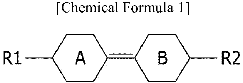
- a liquid crystal composition includes one or more compounds represented by Chemical Formula 1.
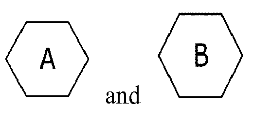
- Chemical Formula 1 are each independently a cyclohexane or tetrahydropyran.
- R1 and R2 are independently hydrogen, a C1 to C8 alkyl group, a C2 to C8 alkenyl group, or a C1 to C8 alkoxy group.
- one or more hydrogen in R1 and R2 may be substituted with F
- one or more -CH 2 - group in R1 and R2 may be substituted with -OCH 2 -, -CF 2 -, and -OCF 2 -
- one or more -CH 3 group group in R1 and R2 may be substituted with -CF 3 or -OCF 3 .
- one or more hydrogen in may be substituted with fluorine (F), or one or more -CH 2 - group in may be substituted with one of -O- or -CF 2 -.
- the compound represented by Chemical Formula 1 may be at least one selected from Chemical Formulas 1-1 to 1-9.
- the compound represented by Chemical Formula 1 may be present in an amount of about 1 wt% to about 40 wt% based on the entire weight of the liquid crystal composition.
- the liquid crystal composition may further include at least one compound selected from Chemical Formulas 2-1 to 2-8.
- R3 and R4 may be independently hydrogen, a C1 to C8 alkyl group, a C2 to C8 alkenyl group, or a C1 to C8 alkoxy group.
- one or more hydrogen in R3 and R4 may be substituted with F
- one or more -CH 2 - group in R3 and R4 may be substituted with one among -OCH 2 -, -CF 2 -, and -OCF 2 -
- one or more -CH 3 group in R3 and R4 may be substituted with -CF 3 or -OCF 3 .
- the compound selected from Chemical Formulas 2-1 to 2-8 may be present in an amount of about 2 wt% to about 40 wt% based on the entire weight of the liquid crystal composition.
- the liquid crystal composition may further include at least one compound selected from Chemical Formulas 3-1 to 3-12.
- R5 and R6 may be independently hydrogen, a C1 to C8 alkyl group, a C2 to C8 alkenyl group, or a C1 to C8 alkoxy group.
- At least one hydrogen in R5 and R6 may be substituted with fluorine.
- the compound of Chemical Formula 3-1 to 3-12 may be present in an amount of about 2 wt% to about 30 wt% based on the entire weight of the liquid crystal composition.
- a liquid crystal display includes a first insulation substrate including a pixel electrode; a second insulation substrate facing the first insulation substrate and including a common electrode; and a liquid crystal layer positioned between the first insulation substrate and the second insulation substrate, wherein the liquid crystal layer includes a liquid crystal composition including one or more compounds represented by Chemical Formula 1.
- Chemical Formula 1 are independently a cyclohexane or tetrahydropyran.
- R1 and R2 are independently hydrogen, a C1 to C8 alkyl group, a C2 to C8 alkenyl group, or a C1 to C8 alkoxy group.
- one or more hydrogen in R1 and R2 is substituted with F
- one or more -CH 2 - group in R1 and R2 is substituted with -OCH 2 -, -CF 2 -, or -OCF 2 -
- one or more -CH 3 group in R1 and R2 is substituted with -CF 3 or -OCF 3 .
- one or more hydrogen in is substituted with F, or one or more -CH 2 -group in is substituted with one of -O- or -CF 2 -.
- the compound represented by Chemical Formula 1 is at least one compound selected from Chemical Formulas 1-1 to 1-9.
- the compound represented by Chemical Formula 1 is present in an amount of about 1 wt% to about 40 wt% based upon the entire weight of the liquid crystal composition.
- the liquid crystal composition in the liquid crystal layer further includes at least one compound selected from Formulas 2-1 to 2-8.
- R3 and R4 are independently hydrogen, a C1 to C8 alkyl group, a C2 to C8 alkenyl group, or a C1 to C8 alkoxy group.
- one or more hydrogen in R3 and R4 is substituted with F
- one or more -CH 2 - group in R3 and R4 is substituted with one among -OCH 2 -, -CF 2 -, and -OCF 2 -
- one or more -CH 3 group in R3 and R4 is substituted with -CF 3 or -OCF 3 .
- compound selected from Chemical Formulas 2-1 to 2-8 is present in an amount of about 2 wt% to about 40 wt% based on the entire weight of the liquid crystal composition.
- the liquid crystal composition in the liquid crystal layer further includes at least one compound selected from Chemical Formulas 3-1 to 3-12.
- R5 and R6 are independently hydrogen, a C1 to C8 alkyl group, a C2 to C8 alkenyl group, or a C1 to C8 alkoxy group.
- At least one hydrogen in R5 and R6 is substituted with fluorine.
- the compound selected from Chemical Formulas 3-1 to 3-12 is present in an amount of about 2 wt% to about 30 wt% based on the entire weight of the liquid crystal composition.
- relative terms such as “lower” or “bottom” and “upper” or “top,” may be used herein to describe one element's relationship to another elements as illustrated in the Figures. It will be understood that relative terms are intended to encompass different orientations of the device in addition to the orientation depicted in the Figures. For example, if the device in one of the figures is turned over, elements described as being on the “lower” side of other elements would then be oriented on “upper” sides of the other elements. The term “lower,” can therefore, encompasses both an orientation of “lower” and “upper,” depending on the particular orientation of the figure.
- Embodiments are described herein with reference to cross section illustrations that are schematic illustrations of idealized embodiments. As such, variations from the shapes of the illustrations as a result, for example, of manufacturing techniques and/or tolerances, are to be expected. Thus, embodiments described herein should not be construed as limited to the particular shapes of regions as illustrated herein but are to include deviations in shapes that result, for example, from manufacturing. For example, a region illustrated or described as flat may, typically, have rough and/or nonlinear features. Moreover, sharp angles that are illustrated may be rounded. Thus, the regions illustrated in the figures are schematic in nature and their shapes are not intended to illustrate the precise shape of a region and are not intended to limit the scope of the present claims.
- a liquid crystal composition includes one or more compounds represented by Chemical Formula 1.
- Chemical Formula 1 are each independently cyclohexane or tetrahydropyran.
- R1 and R2 are independently hydrogen, a C1 to C8 alkyl group (e.g. a C1 to C4 alkyl group), a C2 to C8 alkenyl group (e.g. a C2 to C4 alkenyl group), or a C1 to C8 alkoxy group (e.g. a C1 to C4 alkoxy group).
- a C1 to C8 alkyl group e.g. a C1 to C4 alkyl group
- a C2 to C8 alkenyl group e.g. a C2 to C4 alkenyl group
- a C1 to C8 alkoxy group e.g. a C1 to C4 alkoxy group
- a hydrogen in R1 and R2 may be substituted with F
- a -CH 2 - group may be substituted with -OCH 2 -, -CF 2 -, or -OCF 2 -
- a -CH 3 group may be substituted with -CF 3 or -OCF 3 .
- (one or more) hydrogen included in of Chemical Formula 1 may be substituted with F, and (one or more) -CH 2 - group in may be substituted with one of -O- or -CF 2 -.
- one or more hydrogen in R1 and R2 may be substituted with F
- one or more -CH 2 - group in R1 and R2 may be substituted with -OCH 2 -, -CF 2 -, or -OCF 2 -
- one or more -CH 3 group in R1 and R2 may be substituted with -CF 3 or -OCF 3 .
- the compound of Chemical Formula 1 may be selected from Chemical Formulas 1-1 to Chemical Formula 1-9.
- a process of manufacturing the compound represented by Chemical Formula 1 may include the steps illustrated below.
- the liquid crystal composition may include about 1 wt% to about 40 wt% of the compound represented by Chemical Formula 1 based on the entire weight of the liquid crystal composition. In an embodiment, the liquid crystal composition may include about 5 wt% to about 35 wt% of the compound represented by Chemical Formula 1 based on the entire weight of the liquid crystal composition. In an embodiment, the liquid crystal composition may include about 10 wt% to about 30 wt% of the compound represented by Chemical Formula 1 based on the entire weight of the liquid crystal composition. In an embodiment, the liquid crystal composition may include about 15 wt% to about 25 wt% of the compound represented by Chemical Formula 1 based on the entire weight of the liquid crystal composition.
- each of the compounds represented by Chemical Formula 1 present in the liquid crystal composition is included in an amount of about 1 wt% to about 40 wt% (e.g. about 5 wt% to about 35 wt%, about 10 wt% to about 30 wt%, or about 15 wt% to about 25 wt%) based on the entire weight of the liquid crystal composition.
- the liquid crystal composition may additionally include at least one compound selected from Chemical Formulas 2-1 to 2-8.
- R3 and R4 are independently hydrogen, a C1 to C8 alkyl group (e.g. a C1 to C4 alkyl group), a C2 to C8 alkenyl group (e.g. a C2 to C4 alkenyl group), or a C1 to C8 alkoxy group ( e.g. a C1 to C4 alkoxy group).
- a C1 to C8 alkyl group e.g. a C1 to C4 alkyl group
- a C2 to C8 alkenyl group e.g. a C2 to C4 alkenyl group
- a C1 to C8 alkoxy group e.g. a C1 to C4 alkoxy group
- R3 and R4 may be substituted with F
- (one or more) -CH 2 - group in R3 and R4 may be substituted with -OCH 2 -, -CF 2 -, or -OCF 2 -
- (one or more) -CH 3 group in R3 and R4 may be substituted with -CF 3 or -OCF 3 .
- the compound of Chemical Formula 2-1 to 2-8 may be present in an amount of about 2 wt% to about 40 wt% based on the entire weight of the liquid crystal composition. In an embodiment, Chemical Formula 2-1 to 2-8 may be present in an amount of about 10 wt% to about 30 wt% based on the entire weight of the liquid crystal composition. In an embodiment, Chemical Formula 2-1 to 2-8 may be present in an amount of about 15 wt% to about 25 wt% based on the entire weight of the liquid crystal composition.
- each of the compounds of Chemical Formula 2-1 to 2-8 present in the liquid crystal composition is included in an amount of about 2 wt% to about 40 wt% ( e.g . about 10 wt% to about 30 wt% or about 15 wt% to about 25 wt%) based on the entire weight of the liquid crystal composition.
- the liquid crystal composition of the present invention may additionally include at least one compound selected from Chemical Formulas 3-1 to 3-12.
- R5 and R6 are independently hydrogen, a C1 to C8 alkyl group (e.g. a C1 to C4 alkyl group), a C2 to C8 alkenyl group (e.g. a C2 to C4 alkenyl group), or a C1 to C8 alkoxy group ( e.g. a C1 to C4 alkoxy group).
- a C1 to C8 alkyl group e.g. a C1 to C4 alkyl group
- a C2 to C8 alkenyl group e.g. a C2 to C4 alkenyl group
- a C1 to C8 alkoxy group e.g. a C1 to C4 alkoxy group
- At least one hydrogen in R5 and R6 may be substituted with fluorine.
- a content of the compound of Chemical Formula 3-1 to 3-12 may be about 2 wt% to about 30 wt% based on the entire weight of the liquid crystal composition.
- each of the compounds of Chemical Formula 3-1 to 3-12 present in the liquid crystal composition is included in an amount of about 2 wt% to about 30 wt% ( e.g . about 10 wt% to about 30 wt%, about 20 wt% to about 30 wt%, or about 20 wt% to about 25 wt%) based on the entire weight of the liquid crystal composition.
- liquid crystal composition of the present invention includes the compound represented by Chemical Formula 1.
- the compound represented by Chemical Formula 1 may be formed of two cyclohexane rings connected with a double bond and both having terminal groups. Since the double bond positioned between the two cyclohexane rings is covered by the surrounding hydrogen atoms, the reactivity of the compound is not high and a relatively stable state may be maintained.
- a Comparative Example is a compound having two cyclohexane rings connected by a single bond.
- the liquid crystal composition which includes the compound of Chemical Formula 1 in which two cyclohexane rings are connected by the double bond, was compared to a liquid crystal composition including a compound in which the two cyclohexane rings are connected by a single bond. It was surprisingly found that a liquid crystal composition including the compound of Chemical Formula 1 had improved low temperature stability and low viscosity, thereby improving response speed.
- Table 1 shows a comparison of the physical properties of the compound of the present invention (Embodiment) in which two cyclohexane rings are connected by a double bond and the compound of the Comparative Example in which two cyclohexane rings are connected by a single bond.
- the physical properties of the compounds (molecular weight, dipole moment D, refractive anisotropy ⁇ n, rotational viscosity ⁇ 1, and low temperature stability) were measured. (Table 1) Division Chemical Formula M.W.
- the low temperature stability was improved while the same level of reliability was maintained as compared to the compound having the cyclohexane core with the conventional single bond. That is, the physical properties are excellent and low temperature stability is improved, such that the content in the liquid crystal composition may be increased.
- Table 2 shows the composition of an Embodiment 1 of a liquid crystal composition.
- Table 2 Compound No. Structure of Liquid crystal molecule Content (%) 1 20 2 14 3 22 4 22 5 22
- Table 3 shows the composition of a Comparative Example 1 of a liquid crystal composition. (Table 3) Compound No. Structure of Liquid crystal molecule Content (%) 6 20 7 14 3 22 4 22 5 22
- Table 4 compares the physical properties of the liquid crystal composition of Embodiment 1 having the composition of Table 2 with the physical properties of the liquid crystal composition of Comparative Example 1 having the composition of Table 3.
- the physical properties that were measured include an isotropic phase transition temperature (Tni), a refractive anisotropy ( ⁇ n), a dielectric anisotropy ( ⁇ ), a rotational viscosity ⁇ 1, a low temperature stability (LTS), and a voltage holding rate (VHR).
- Tni isotropic phase transition temperature
- ⁇ n refractive anisotropy
- ⁇ dielectric anisotropy
- VHR voltage holding rate
- the liquid crystal composition according to the Embodiment 1 was equal to or better than the liquid crystal composition according to the Comparative Example 1 with respect to all physical properties except for Tni.
- the low temperature stability was significantly improved as compared to the liquid crystal composition of Comparative Example 1.
- the cyclohexane groups are connected with a single bond (compound Nos. 6 and 7 of Table 3).
- the low temperature stability of the compound is low, and therefore even when the liquid crystal composition is included in an excessive amount, since the low temperature stability is decreased, a sufficient amount of the compound may not be present in the liquid crystal composition.
- the cyclohexane groups are connected with a double bond (compound Nos. 1 and 2 of Table 2).
- This compound has excellent low temperature stability.
- Tables 2 to 4 when the Embodiment 1 liquid crystal composition including this compound is included in an excessive amount, the low temperature stability is even better than the liquid crystal composition of Comparative Example 1.
- the improved low temperature stability allows for easy storage and distribution of the liquid crystal composition, thereby improving its economic viability.
- the compounds 1 and 2 of Table 2 and the compounds 5 and 6 of Table 3 are compounds that decrease the viscosity of the liquid crystal composition and contribute to the reaction speed.
- the response speed of the liquid crystal and the rotational viscosity of the liquid crystal are related as follows. That is, if a cell gap d of the liquid crystal is increased, the response speed of the liquid crystal is increased, and if the rotational viscosity ⁇ 1 is increased, the response speed of the liquid crystal is increased. ⁇ off ⁇ ⁇ 1 d 2 K 33
- the compounds of the embodiment have a lower rotational viscosity than the compounds of the Comparative Example. Accordingly, the response speed of the liquid crystal may be decreased.
- the liquid crystal composition according to the embodiment of the present invention may include a greater range of the compound contributing to the reaction speed.
- the compound of Chemical Formula 1 of the present invention includes the cyclohexane groups connected with a double bond such that the low temperature stability is excellent, and the low temperature stability of the liquid crystal composition may be maintained even if an excessive amount of the compound is included.
- the liquid crystal composition according to the present invention includes the compound in which the cyclohexane groups are connected with a double bond such that the low temperature stability is excellent and the reaction speed is also improved as compared to the liquid crystal composition according to the conventional Comparative Example 1.
- the structure of the described liquid crystal display is only one example and the embodiment of the liquid crystal display may be clearly used without being limited to the case of a vertical alignment ("VA") mode liquid crystal display.
- VA vertical alignment
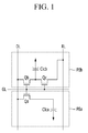
- FIG. 1 is an equivalent circuit diagram for one pixel of a liquid crystal display according to an embodiment of the present invention.
- one pixel PX of the liquid crystal display includes: a plurality of signal lines, including a gate line GL for transferring a gate signal, a data line DL for transferring a data signal, and a voltage division reference voltage line RL for transferring a voltage division reference voltage; first, second, and third switching elements Qa, Qb, and Qc; and first and second liquid crystal capacitors Clca and Clcb connected to the plurality of signal lines.
- the first and second switching elements Qa and Qb are connected to the gate line GL and the data line DL, respectively, and the third switching element Qc is connected to the output terminal of the second switching element Qb and to the voltage division reference voltage line RL.
- the first switching element Qa and the second switching element Qb are three-terminal elements, such as a thin film transistor. Control terminals thereof are connected to the gate line GL, input terminals thereof are connected to the data line DL, an output terminal of the first switching element Qa is connected to a first liquid crystal capacitor Clca, and an output terminal of the second switching element Qb is connected to a second liquid crystal capacitor Clcb and an input terminal of the third switching element Qc.
- the third switching element Qc is also a three-terminal element, such as a thin film transistor, and the control terminal thereof is connected to the gate line GL, the input terminal thereof is connected to the second liquid crystal capacitor Clcb, and an output terminal thereof is connected to the voltage division reference voltage line RL.
- the first switching element Qa, the second switching element Qb, and the third switching element Qc connected to the gate line GL are turned on. Accordingly, a data voltage applied to the data line DL is applied to a first subpixel electrode PEa and a second subpixel electrode PEb through the turned-on first switching element Qa and second switching element Qb.
- the data voltages applied to the first subpixel electrode PEa and the second subpixel electrode PEb are the same, and the first liquid crystal capacitor Clca and the second liquid crystal capacitor Clcb are charged to the same value as the difference between the common voltage and the data voltage.
- the voltage charged in the second liquid crystal capacitor Clcb is divided through the turned-on third switching element. Accordingly, the voltage value charged in the second liquid crystal capacitor Clcb is decreased by the difference between the common voltage and the voltage division reference voltage. That is, the voltage charged in the first liquid crystal capacitor Clca is higher than a voltage charged in the second liquid crystal capacitor Clcb.
- the voltage charged in the first liquid crystal capacitor Clca and the voltage charged in the second liquid crystal capacitor Clcb are different from each other. Since the voltage of the first liquid crystal capacitor Clca and the voltage of the second liquid crystal capacitor Clcb are different from each other, inclination angles of liquid crystal molecules in the first subpixel and the second subpixel become different from each other, thus luminance of the two subpixels also become different from each other. Accordingly, when the voltage of the first liquid crystal capacitor Clca and the voltage of the second liquid crystal capacitor Clcb are appropriately adjusted, an image viewed from the side may be as close as possible to an image viewed from the front, thereby improving side visibility.
- the liquid crystal display in order to make the voltage charged in the first liquid crystal capacitor Clca and the voltage charged in the second liquid crystal capacitor Clcb different from each other, the liquid crystal display includes the third switching element Qc connected to the second liquid crystal capacitor Clcb and the voltage division reference voltage line RL.
- the second liquid crystal capacitor Clcb may be connected to a step-down capacitor.
- the liquid crystal display includes the third switching element Qc including a first terminal connected to a step-down gate line, a second terminal connected to the second liquid crystal capacitor Clcb, and a third terminal connected to the step-down capacitor, and a portion of the amount of charge charged in the second liquid crystal capacitor Clcb is charged in the step-down capacitor, so that the charging voltages between the first liquid crystal capacitor Clcb and the second liquid crystal capacitor Clcb may be set differently.
- the first liquid crystal capacitor Clca and the second liquid crystal capacitor Clcb are connected to different data lines and receive different data voltages, thus the charging voltages between the first liquid crystal capacitor Clca and the second liquid crystal capacitor Clcb may be set differently.
- the charging voltages between the first liquid crystal capacitor Clca and the second liquid crystal capacitor Clcb may be set differently by various other methods.
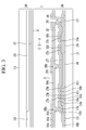
- FIG. 2 is a plan view of an embodiment of a liquid crystal display according to the present invention
- FIG. 3 is a cross-sectional view of the liquid crystal display of FIG. 2 taken along line III-III.
- FIG. 4 is a top plan view of an embodiment of a basic region of a pixel electrode in a lower panel according to the present invention.
- a gate conductor including a gate line 121 and a voltage division reference voltage line 131 are formed on an insulating substrate 110.
- the insulating substrate 110 is formed of transparent glass, plastics, or the like.
- the gate line 121 includes a first gate electrode 124a, a second gate electrode 124b, a third gate electrode 124c, and a wide end portion (not illustrated) for connection to another layer or an external driving circuit.
- the voltage division reference voltage line 131 includes first storage electrodes 135 and 136, and a reference electrode 137. Second storage electrodes 138 and 139, which are not connected to the voltage division reference voltage line 131, but which overlap the second subpixel electrode 191b, are positioned on the lower panel 100.
- a gate insulating layer 140 is formed on the gate line 121 and the voltage division reference voltage line 131.
- a first semiconductor 154a, a second semiconductor 154b, and a third semiconductor 154c are formed on the gate insulating layer 140.
- a plurality of ohmic contacts 163a, 165a, 163b, 165b, 163c, and 165c are formed on the semiconductors 154a, 154b, and 154c.
- a plurality of data lines 171 including a first source electrode 173a and a second source electrode 173b, and data conductors including a first drain electrode 175a, a second drain electrode 175b, a third source electrode 173c, and a third drain electrode 175c are formed on the ohmic contacts 163a, 165a, 163b, 165b, 163c, and 165c, and the gate insulating layer 140.
- the data conductors, as well as the semiconductors and the ohmic contacts positioned under the data conductors, may be simultaneously formed by using one mask.
- the data line 171 includes a wide end portion (not illustrated) for connection with another layer or an external driving circuit.
- the first gate electrode 124a, the first source electrode 173a, and the first drain electrode 175a form a first thin film transistor Qa together with the first semiconductor 154a, and a channel of the thin film transistor is formed on the semiconductor 154a between the first source electrode 173a and the first drain electrode 175a.
- the second gate electrode 124b, the second source electrode 173b, and the second drain electrode 175b form a second thin film transistor Qb together with the second semiconductor 154b, and a channel of the thin film transistor is formed on the semiconductor 154b between the second source electrode 173b and the second drain electrode 175b.
- the third gate electrode 124c, the third source electrode 173c, and the third drain electrode 175c form a third thin film transistor Qc together with the third semiconductor 154c, and a channel of the thin film transistor is formed on the semiconductor 154c between the third source electrode 173c and the third drain electrode 175c.
- the second drain electrode 175b is connected with the third source electrode 173c, and includes an extended portion 177 that widely extends.
- a first passivation layer 180p is formed on the data conductors 171, 173c, 175a, 175b, and 175c and exposed portions of the semiconductors 154a, 154b, and 154c.
- the first passivation layer 180p may include an inorganic insulating layer, such as a silicon nitride or a silicon oxide.
- the first passivation layer 180p may prevent a pigment of a color filter 230 from flowing into the exposed portions of the semiconductors 154a, 154b, and 154c.
- the color filter 230 is formed on the first passivation layer 180p.
- the color filter 230 extends in a vertical direction along two adjacent data lines.
- a first light blocking member 220 is positioned on the first passivation layer 180p, an edge of the color filter 230, and the data line 171.
- the color filter 230 may not be formed on the lower display panel 100, but rather may be on the upper display panel 200.
- a second passivation layer 180q is formed on the color filter 230.
- the second passivation layer 180q may include an inorganic insulating layer such as a silicon nitride or a silicon oxide.
- the second passivation layer 180q prevents lifting of the color filter 230 and reduces pollution of the liquid crystal layer 3 due to an organic material such as a solvent flowing from the color filter 230, thereby preventing defects such as afterimage, which may be generated when a screen is driven.
- a first contact hole 185a and a second contact hole 185b that expose the first drain electrode 175a and the second drain electrode 175b are formed in the first passivation layer 180p and the second passivation layer 180q.
- a third contact hole 185c that exposes a portion of the reference electrode 137 and a portion of the third drain electrode 175c is formed in the first passivation layer 180p, the second passivation layer 180q, and the gate insulating layer 140.
- the third contact hole 185c is covered by a connecting member 195.
- the connecting member 195 electrically connects the reference electrode 137 and the third drain electrode 175c exposed through the third contact hole 185c.
- a plurality of pixel electrodes 191 is formed on the second passivation layer 180q.
- Each of the pixel electrodes 191 includes a first sub-pixel electrode 191a and a second sub-pixel electrode 191b that are spaced apart from each other with the gate line 121 included therebetween.
- the sub-pixel electrodes 191a and 191b are adjacent to each other in a column direction with respect to the gate line 121.
- the pixel electrodes 191 may be formed of a transparent conductive material such as indium tin oxide ("ITO"), indium zinc oxide (“IZO”) or the like, or a reflective metal such as aluminum, silver, chromium, or an alloy thereof.
- ITO indium tin oxide
- IZO indium zinc oxide
- a reflective metal such as aluminum, silver, chromium, or an alloy thereof.
- the first sub-pixel electrode 191a and the second sub-pixel electrode 191b each include a basic electrode as illustrated in FIG. 4 or alternatively, at least one electrode modified based on the basic electrode.
- the first sub-pixel electrode 191a and the second sub-pixel electrode 191b are respectively physically and electrically connected to the first drain electrode 175a and the second drain electrode 175b via the first contact hole 185a and the second contact hole 185b, and receive a data voltage from the first drain electrode 175a and the second drain electrode 175b.
- a portion of the data voltage applied to the second drain electrode 175b is divided by the third source electrode 173c so that a voltage applied to the first sub-pixel electrode 191a is greater than a voltage applied to the second sub-pixel electrode 191b.
- Luminance of light that passes through the liquid crystal layer 3 is varied according to a direction of liquid crystal molecules that is determined as described above.
- a lower alignment layer 11 is coated on the pixel electrode 191.
- the overall shape of the basic electrode 199 is a quadrangle, and includes a cross-shaped stem having a transverse stem 193 and a longitudinal stem 192 that are crossed. Further, the basic electrode 199 is divided into a first subregion Da, a second subregion Db, a third subregion Dc, and a fourth subregion Dd by the horizontal stem portion 193 and the vertical stem portion 192, and each of the subregions Da to Dd includes a plurality of first fine branch portions 194a, a plurality of second fine branch portions 194b, a plurality of third fine branch portions 194c, and a plurality of fourth fine branch portions 194d.
- the first fine branch portions 194a extend obliquely in an upper left direction from the horizontal stem portion 193 or the vertical stem portion 192
- the second fine branch portions 194b extend obliquely in an upper right direction from the horizontal stem portion 193 or the vertical stem portion 192
- the third fine branch portions 194c extend in a lower left direction from the horizontal stem portion 193 or the vertical stem portion 192
- the fourth fine branch portions 194d extend obliquely in a lower right direction from the horizontal stem portion 193 or the vertical stem portion 192.
- the first to fourth fine branch portions 194a, 194b, 194c, and 194d form an angle of approximately 45° or 135° with gate lines 121a and 121b or the horizontal stem portion 193. Further, the fine branch portions 194a, 194b, 194c, and 194d of the two adjacent subregions Da, Db, Dc, and Dd may be positioned orthogonal to each other.
- the width of the fine branch portions 194a, 194b, 194c, and 194d may be in the range of about 2.5 to about 5.0 micrometers ( ⁇ m) and the gap between the adjacent fine branch portions 194a, 194b, 194c, and 194d in one of the subregions Da, Db, Dc, or Dd may be in the range of about 2.5 to about 5.0 ⁇ m.
- the widths of the fine branch portions 194a, 194b, 194c, and 194d may be increased to be closer to the horizontal stem portion 193 or the vertical stem portion 192, and a difference between the width of the widest portion and the width of the narrowest portion in one of the fine branch portions 194a, 194b, 194c, or 194d, may be in the range of about 0.2 to about 1.5 ⁇ m.
- the first subpixel electrode 191a and the second subpixel electrode 191b are connected to the first drain electrode 175a and the second drain electrode 175b through the first contact hole 185a and the second contact hole 185b, respectively, and receive the data voltage from the first drain electrode 175a and the second drain electrode 175b, respectively.
- sides of the first to the fourth fine branch portions 194a, 194b, 194c, and 194d distort the electric field and makes a horizontal component of the electric field that determines the inclination direction of the liquid crystal molecules 31.
- the horizontal component of the electric field is substantially horizontal to the sides of the first to fourth fine branch portions 194a, 194b, 194c, and 194d. Accordingly, as illustrated in FIG.
- the liquid crystal molecules 31 are inclined in a direction parallel to the longitudinal direction of the fine branch portions 194a, 194b, 194c, and 194d. Since one basic electrode 199 includes four subregions Da to Dd, in which longitudinal directions of the fine branch portions 194a, 194b, 194c, and 194d are different from each other, the liquid crystal molecules 31 are inclined in about four different directions, and four domains, in which the alignment direction of the liquid crystal molecules 31 differ from each other, are formed in the liquid crystal layer 3. As described above, when the inclination direction of the liquid crystal molecules is diversified, a reference viewing angle of the liquid crystal display is increased.
- a black matrix 220 is formed on the insulation substrate 210.
- the black matrix 220 is formed on the upper panel 220 to correspond to a region of the lower panel 100 in which the data lines are formed and a region in which transistors or the like are formed.
- An overcoat layer 250 is formed on the black matrix 220.
- the overcoat layer 250 may be omitted.
- the common electrode 270 is formed on the overcoat layer 250.
- An upper alignment layer 21 is formed on the common electrode 270.
- the liquid crystal layer 3 is formed between the lower panel 100 and the upper panel 200. Now, the liquid crystal layer 3 including an embodiment of the liquid crystal composition according to the present invention will be described.
- the liquid crystal layer 3 includes a liquid crystal composition including one or more compound represented by Chemical Formula 1.
- Chemical Formula 1 are independently a cyclohexane or tetrahydropyran.
- R1 and R2 are each independently hydrogen, a C1 to C8 alkyl group, a C2 to C8 alkenyl group, or a C1 to C8 alkoxy group.
- a hydrogen in R1 and R2 may be substituted with F, a -CH 2 - group may be substituted with -OCH 2 -, -CF 2 -, or -OCF 2 -, and a -CH 3 group may be substituted with -CF 3 or -OCF 3 . .
- (one or more) hydrogen in may be substituted with F
- (one or more) -CH 2 - group in may be substituted with one of -O- or -CF 2 -.
- one or more hydrogen in R1 and R2 may be substituted with F
- one or more -CH 2 - group in R1 and R2 may be substituted with -OCH 2 -, -CF 2 -, or -OCF 2 -
- one or more -CH 3 group in R1 and R2 may be substituted with -CF 3 or -OCF 3 .
- the compound of Chemical Formula 1 may be selected from Chemical Formula 1-1 to Chemical Formula 1-9.
- the compound of Chemical Formula 1 may be present in an amount of about 1 wt% to about 40 wt% based on the entire weight of the liquid crystal composition.
- the liquid crystal composition of the liquid crystal layer of the liquid crystal display may additionally include at least one compound selected from Chemical Formulas 2-1 to 2-8.
- R3 and R4 are independently hydrogen, a C1 to C8 alkyl group, a C2 to C8 alkenyl group, or a C1 to C8 alkoxy group.
- a hydrogen included in R3 and R4 may be substituted with F, a -CH 2 - group in R3 and R4 may be substituted with -OCH 2 -, -CF 2 -, or -OCF 2 -, and a -CH 3 group in R3 and R4 may be substituted with -CF 3 or -OCF 3 .
- the compound of Chemical Formula 2-1 to 2-8 may be present in an amount of about 2 wt% to about 40 wt% based on the entire weight of the liquid crystal composition.
- the liquid crystal composition of the liquid crystal layer may additionally include at least one compound selected from Chemical Formulas 3-1 to 3-12.
- R5 and R6 are independently hydrogen, a C1 to C8 alkyl group, a C2 to C8 alkenyl group, or a C1 to C8 alkoxy group.
- At least one hydrogen included in R5 and R6 may be substituted with fluorine.
- the compound selected from Chemical Formulas 3-1 to 3-12 may be present in an amount of about 2 wt% to about 30 wt% based on the entire weight of the liquid crystal composition.
- the rotational viscosity of the liquid crystal layer is low compared to the conventional liquid crystal display, thereby improving the response speed of the liquid crystal display.
- the liquid crystal display having the structure illustrated in FIG. 1 to FIG. 4 is only one example and the liquid crystal composition according to the present invention may be clearly applied to other liquid crystal displays, without being limited to only the vertical alignment (VA) mode liquid crystal display in which the pixel electrode is positioned in the first display panel and the common electrode is positioned in the second display panel.
- VA vertical alignment
Landscapes
- Chemical & Material Sciences (AREA)
- Organic Chemistry (AREA)
- Crystallography & Structural Chemistry (AREA)
- Engineering & Computer Science (AREA)
- Materials Engineering (AREA)
- Physics & Mathematics (AREA)
- Nonlinear Science (AREA)
- General Physics & Mathematics (AREA)
- Mathematical Physics (AREA)
- Optics & Photonics (AREA)
- Geometry (AREA)
- Liquid Crystal Substances (AREA)
- Liquid Crystal (AREA)
Abstract

R1 and R2 are each independently hydrogen, a C1 to C8 alkyl group, a C2 to C8 alkenyl group, or a C1 to C8 alkoxy group.
Description
- The present invention relates to a liquid crystal composition and a liquid crystal display device including the same.
- A liquid crystal display ("LCD") is a popular type of flat panel display. The liquid crystal display is capable of determining a direction of the liquid crystal molecules of the liquid crystal layer and controlling transmittance of light passing through the liquid crystal layer by applying a voltage to the field generating electrodes to generate an electric field in the liquid crystal layer.
- The liquid crystal layer allows the liquid crystal display to achieve a desired image by controlling the transmittance of light. In particular, various characteristics are desirable for the liquid crystal displays, such as, low-voltage driving, high voltage holding ratio ("VHR"), a wide viewing angle, a wide operation temperature range, and high-speed response.
- To obtain a high speed response characteristic for a liquid crystal display, it is desirable to improve the physical properties of the liquid crystal layer, such as, rotational viscosity, refractive index, and elastic coefficient.
- The present invention provides a liquid crystal composition capable of achieving a high speed response characteristic and low temperature stability, and a display device including the same.
- In embodiments, a liquid crystal composition includes one or more compounds represented by Chemical Formula 1.

- In Chemical Formula 1,

- In Chemical Formula 1, R1 and R2 are independently hydrogen, a C1 to C8 alkyl group, a C2 to C8 alkenyl group, or a C1 to C8 alkoxy group.
- In one embodiment, in the compound of Chemical Formula 1, one or more hydrogen in R1 and R2 may be substituted with F, one or more -CH2- group in R1 and R2 may be substituted with -OCH2-, -CF2-, and -OCF2-, and one or more -CH3 group group in R1 and R2 may be substituted with -CF3 or -OCF3.
- In an embodiment, in the compound of Chemical Formula 1, one or more hydrogen in

- In an embodiment, the compound represented by Chemical Formula 1 may be at least one selected from Chemical Formulas 1-1 to 1-9.


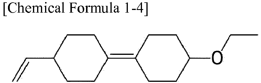

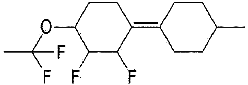


- In an embodiment, the compound represented by Chemical Formula 1 may be present in an amount of about 1 wt% to about 40 wt% based on the entire weight of the liquid crystal composition.
- In an embodiment, the liquid crystal composition may further include at least one compound selected from Chemical Formulas 2-1 to 2-8.


- In Chemical Formulas 2-1 to 2-8, R3 and R4 may be independently hydrogen, a C1 to C8 alkyl group, a C2 to C8 alkenyl group, or a C1 to C8 alkoxy group.
- In an embodiment, one or more hydrogen in R3 and R4 may be substituted with F, one or more -CH2- group in R3 and R4 may be substituted with one among -OCH2-, -CF2-, and -OCF2-, or one or more -CH3 group in R3 and R4 may be substituted with -CF3 or -OCF3.
- In an embodiment, the compound selected from Chemical Formulas 2-1 to 2-8 may be present in an amount of about 2 wt% to about 40 wt% based on the entire weight of the liquid crystal composition.
- In an embodiment, the liquid crystal composition may further include at least one compound selected from Chemical Formulas 3-1 to 3-12.


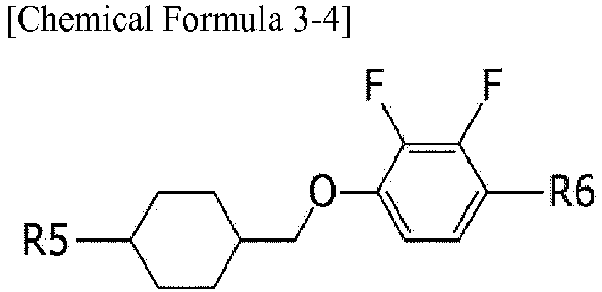


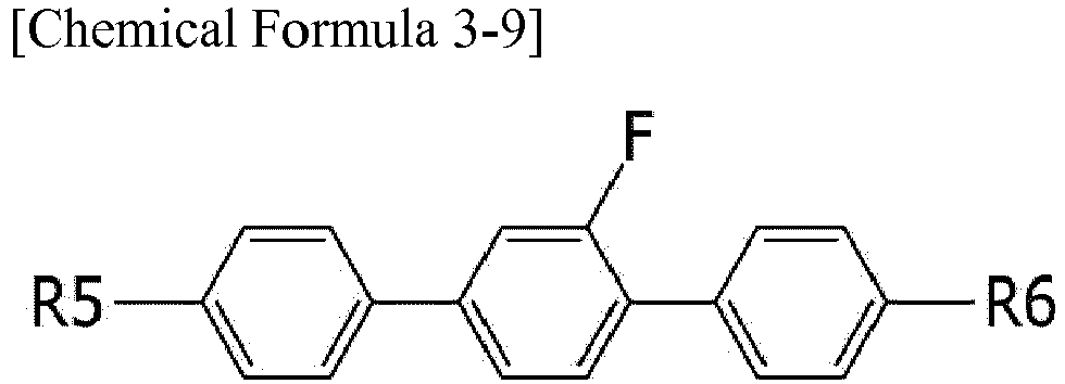


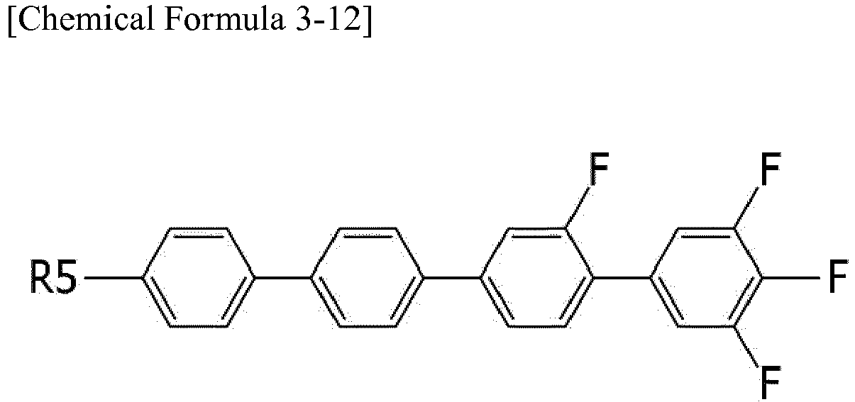
- In Chemical Formulas 3-1 to 3-12, R5 and R6 may be independently hydrogen, a C1 to C8 alkyl group, a C2 to C8 alkenyl group, or a C1 to C8 alkoxy group.
- In an embodiment, at least one hydrogen in R5 and R6 may be substituted with fluorine.
- In an embodiment, the compound of Chemical Formula 3-1 to 3-12 may be present in an amount of about 2 wt% to about 30 wt% based on the entire weight of the liquid crystal composition.
- In embodiments, a liquid crystal display includes a first insulation substrate including a pixel electrode; a second insulation substrate facing the first insulation substrate and including a common electrode; and a liquid crystal layer positioned between the first insulation substrate and the second insulation substrate, wherein the liquid crystal layer includes a liquid crystal composition including one or more compounds represented by Chemical Formula 1.

- In Chemical Formula 1,

- In Chemical Formula 1, R1 and R2 are independently hydrogen, a C1 to C8 alkyl group, a C2 to C8 alkenyl group, or a C1 to C8 alkoxy group.
- In an embodiment, in the compound of Chemical Formula 1, one or more hydrogen in R1 and R2 is substituted with F, one or more -CH2- group in R1 and R2 is substituted with -OCH2-, -CF2-, or -OCF2-, and one or more -CH3 group in R1 and R2 is substituted with -CF3 or -OCF3.
- In an embodiment, in the compound of Chemical Formula 1, one or more hydrogen in


- In an embodiment, the compound represented by Chemical Formula 1 is at least one compound selected from Chemical Formulas 1-1 to 1-9.


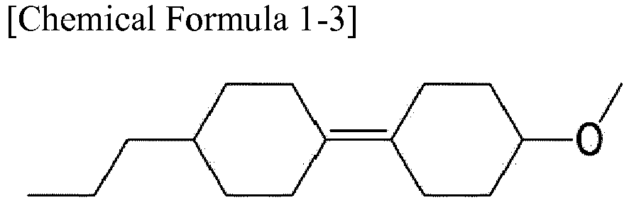


- In an embodiment, the compound represented by Chemical Formula 1 is present in an amount of about 1 wt% to about 40 wt% based upon the entire weight of the liquid crystal composition.
- In an embodiment, the liquid crystal composition in the liquid crystal layer further includes at least one compound selected from Formulas 2-1 to 2-8.


- In Chemical Formula 2-1 to 2-8, R3 and R4 are independently hydrogen, a C1 to C8 alkyl group, a C2 to C8 alkenyl group, or a C1 to C8 alkoxy group.
- In an embodiment, one or more hydrogen in R3 and R4 is substituted with F, one or more -CH2- group in R3 and R4 is substituted with one among -OCH2-, -CF2-, and -OCF2-, or one or more -CH3 group in R3 and R4 is substituted with -CF3 or -OCF3.
- In an exemplary embodiment, compound selected from Chemical Formulas 2-1 to 2-8 is present in an amount of about 2 wt% to about 40 wt% based on the entire weight of the liquid crystal composition.
- In an embodiment, the liquid crystal composition in the liquid crystal layer further includes at least one compound selected from Chemical Formulas 3-1 to 3-12.


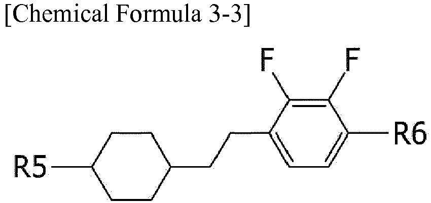


- In Chemical Formula 3-1 to 3-12, R5 and R6 are independently hydrogen, a C1 to C8 alkyl group, a C2 to C8 alkenyl group, or a C1 to C8 alkoxy group.
- In an embodiment, at least one hydrogen in R5 and R6 is substituted with fluorine.
- In an embodiment, the compound selected from Chemical Formulas 3-1 to 3-12 is present in an amount of about 2 wt% to about 30 wt% based on the entire weight of the liquid crystal composition.
At least some of the above and other features of the invention are set out in the claims. - The above and other aspects, advantages and features of this disclosure will become more apparent by describing in further detail embodiments thereof with reference to the accompanying drawings, in which:
-
FIG. 1 is an equivalent circuit diagram of one pixel of an embodiment of a liquid crystal display according to the present invention. -
FIG. 2 is a plan view of an embodiment of a liquid crystal display according to the present invention. -
FIG. 3 is a cross-sectional view of the liquid crystal display ofFIG. 2 taken along line III-III. -
FIG. 4 is a top plan view of an embodiment of a basic region of a pixel electrode in a lower panel according to the present invention. - The present invention will be described more fully hereinafter with reference to the accompanying drawings, in which various embodiments are shown. As those skilled in the art would realize, the described embodiments may be modified in various different ways, all without departing from the scope of the present invention. Rather, these embodiments are provided so that this disclosure will be thorough and complete, and will fully convey the scope of the invention to those skilled in the art. Like reference numerals refer to like elements throughout.
- In the drawings, the thickness of layers, films, panels, regions, etc., are exaggerated for clarity. Like reference numerals designate like elements throughout the specification. It will be understood that when an element such as a layer, film, region, or substrate is referred to as being "on" another element, it can be directly on the other element or intervening elements may also be present. In contrast, when an element is referred to as being "directly on" another element, there are no intervening elements present.
- It will be understood that, although the terms "first," "second," "third" etc. may be used herein to describe various elements, components, regions, layers and/or sections, these elements, components, regions, layers and/or sections should not be limited by these terms. These terms are only used to distinguish one element, component, region, layer or section from another element, component, region, layer or section. Thus, "a first element," "component," "region," "layer" or "section" discussed below could be termed a second element, component, region, layer or section without departing from the teachings herein.
- The terminology used herein is for the purpose of describing particular embodiments only and is not intended to be limiting. As used herein, the singular forms "a," "an," and "the" are intended to include the plural forms, including "at least one," unless the content clearly indicates otherwise. "Or" means "and/or." As used herein, the term "and/or" includes any and all combinations of one or more of the associated listed items. It will be further understood that the terms "comprises" and/or "comprising," or "includes" and/or "including" when used in this specification, specify the presence of stated features, regions, integers, steps, operations, elements, and/or components, but do not preclude the presence or addition of one or more other features, regions, integers, steps, operations, elements, components, and/or groups thereof.
- Furthermore, relative terms, such as "lower" or "bottom" and "upper" or "top," may be used herein to describe one element's relationship to another elements as illustrated in the Figures. It will be understood that relative terms are intended to encompass different orientations of the device in addition to the orientation depicted in the Figures. For example, if the device in one of the figures is turned over, elements described as being on the "lower" side of other elements would then be oriented on "upper" sides of the other elements. The term "lower," can therefore, encompasses both an orientation of "lower" and "upper," depending on the particular orientation of the figure. Similarly, if the device in one of the figures is turned over, elements described as "below" or "beneath" other elements would then be oriented "above" the other elements. The terms "below" or "beneath" can, therefore, encompass both an orientation of above and below.
- "About" or "approximately" as used herein is inclusive of the stated value and means within an acceptable range of deviation for the particular value as determined by one of ordinary skill in the art, considering the measurement in question and the error associated with measurement of the particular quantity (i.e., the limitations of the measurement system). For example, "about" can mean within one or more standard deviations, or within ± 30%, 20%, 10%, 5% of the stated value.
- Unless otherwise defined, all terms (including technical and scientific terms) used herein have the same meaning as commonly understood by one of ordinary skill in the art to which this disclosure belongs. It will be further understood that terms, such as those defined in commonly used dictionaries, should be interpreted as having a meaning that is consistent with their meaning in the context of the relevant art and the present disclosure, and will not be interpreted in an idealized or overly formal sense unless expressly so defined herein.
- Embodiments are described herein with reference to cross section illustrations that are schematic illustrations of idealized embodiments. As such, variations from the shapes of the illustrations as a result, for example, of manufacturing techniques and/or tolerances, are to be expected. Thus, embodiments described herein should not be construed as limited to the particular shapes of regions as illustrated herein but are to include deviations in shapes that result, for example, from manufacturing. For example, a region illustrated or described as flat may, typically, have rough and/or nonlinear features. Moreover, sharp angles that are illustrated may be rounded. Thus, the regions illustrated in the figures are schematic in nature and their shapes are not intended to illustrate the precise shape of a region and are not intended to limit the scope of the present claims.
- Embodiments of a liquid crystal composition and a liquid crystal display including the liquid crystal composition are described with reference to the accompanying drawings.
- In an embodiment, a liquid crystal composition includes one or more compounds represented by Chemical Formula 1.

- In Chemical Formula 1,

- In Chemical Formula 1, R1 and R2 are independently hydrogen, a C1 to C8 alkyl group (e.g. a C1 to C4 alkyl group), a C2 to C8 alkenyl group (e.g. a C2 to C4 alkenyl group), or a C1 to C8 alkoxy group (e.g. a C1 to C4 alkoxy group).
- In Chemical Formula 1, a hydrogen in R1 and R2 may be substituted with F, a -CH2- group may be substituted with -OCH2-, -CF2-, or -OCF2-, and a -CH3 group may be substituted with -CF3 or -OCF3.
- Also, (one or more) hydrogen included in


- In Chemical Formula 1, one or more hydrogen in R1 and R2 may be substituted with F, one or more -CH2- group in R1 and R2 may be substituted with -OCH2-, -CF2-, or -OCF2-, and one or more -CH3 group in R1 and R2 may be substituted with -CF3 or -OCF3.
- The compound of Chemical Formula 1 may be selected from Chemical Formulas 1-1 to Chemical Formula 1-9.




- A process of manufacturing the compound represented by Chemical Formula 1 may include the steps illustrated below.

- However, the above manufacturing process is only one possible example, and the compound of Chemical Formula 1 may also be manufactured by other manufacturing processes.
- In an embodiment, the liquid crystal composition may include about 1 wt% to about 40 wt% of the compound represented by Chemical Formula 1 based on the entire weight of the liquid crystal composition. In an embodiment, the liquid crystal composition may include about 5 wt% to about 35 wt% of the compound represented by Chemical Formula 1 based on the entire weight of the liquid crystal composition. In an embodiment, the liquid crystal composition may include about 10 wt% to about 30 wt% of the compound represented by Chemical Formula 1 based on the entire weight of the liquid crystal composition. In an embodiment, the liquid crystal composition may include about 15 wt% to about 25 wt% of the compound represented by Chemical Formula 1 based on the entire weight of the liquid crystal composition. In embodiments of the present invention in which the liquid crystal composition includes more than one compound represented by Chemical Formula 1, each of the compounds represented by Chemical Formula 1 present in the liquid crystal composition is included in an amount of about 1 wt% to about 40 wt% (e.g. about 5 wt% to about 35 wt%, about 10 wt% to about 30 wt%, or about 15 wt% to about 25 wt%) based on the entire weight of the liquid crystal composition.
- In one embodiment, the liquid crystal composition may additionally include at least one compound selected from Chemical Formulas 2-1 to 2-8.


- In Chemical Formulas 2-1 to 2-8, R3 and R4 are independently hydrogen, a C1 to C8 alkyl group (e.g. a C1 to C4 alkyl group), a C2 to C8 alkenyl group (e.g. a C2 to C4 alkenyl group), or a C1 to C8 alkoxy group (e.g. a C1 to C4 alkoxy group).
- In Chemical Formulas 2-1 to 2-8, at least one hydrogen in R3 and R4 may be substituted with F, (one or more) -CH2- group in R3 and R4 may be substituted with -OCH2-, -CF2-, or -OCF2-, and (one or more) -CH3 group in R3 and R4 may be substituted with -CF3 or -OCF3.
- Also, in the liquid crystal composition of the present invention, the compound of Chemical Formula 2-1 to 2-8 may be present in an amount of about 2 wt% to about 40 wt% based on the entire weight of the liquid crystal composition. In an embodiment, Chemical Formula 2-1 to 2-8 may be present in an amount of about 10 wt% to about 30 wt% based on the entire weight of the liquid crystal composition. In an embodiment, Chemical Formula 2-1 to 2-8 may be present in an amount of about 15 wt% to about 25 wt% based on the entire weight of the liquid crystal composition. In embodiments of the present invention in which the liquid crystal composition includes more than one compound of Chemical Formula 2-1 to 2-8, each of the compounds of Chemical Formula 2-1 to 2-8 present in the liquid crystal composition is included in an amount of about 2 wt% to about 40 wt% (e.g. about 10 wt% to about 30 wt% or about 15 wt% to about 25 wt%) based on the entire weight of the liquid crystal composition.The liquid crystal composition of the present invention may additionally include at least one compound selected from Chemical Formulas 3-1 to 3-12.

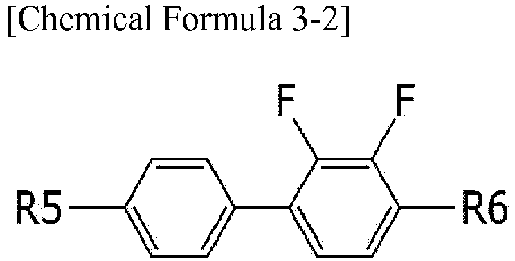
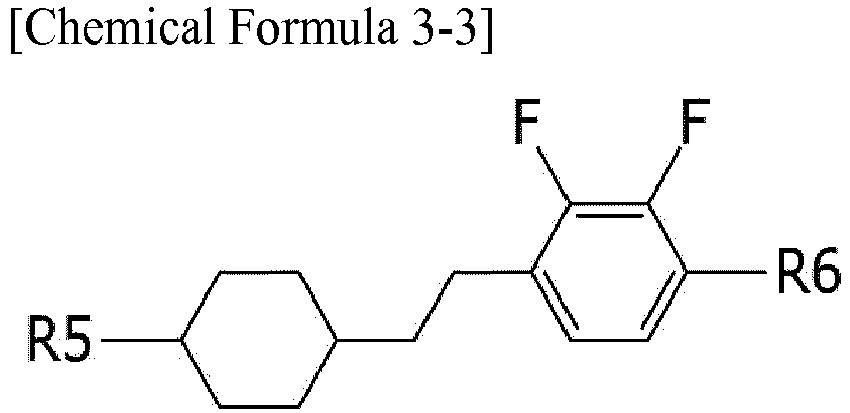


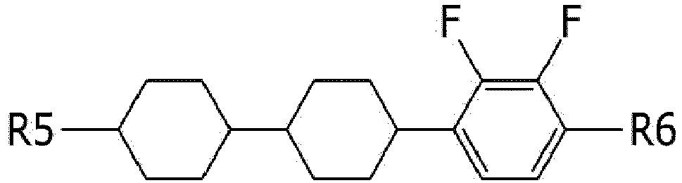


- In Chemical Formula 3-1 to 3-12, R5 and R6 are independently hydrogen, a C1 to C8 alkyl group (e.g. a C1 to C4 alkyl group), a C2 to C8 alkenyl group (e.g. a C2 to C4 alkenyl group), or a C1 to C8 alkoxy group (e.g. a C1 to C4 alkoxy group).
- Also, at least one hydrogen in R5 and R6 may be substituted with fluorine.
- In the liquid crystal composition of the present invention, a content of the compound of Chemical Formula 3-1 to 3-12 may be about 2 wt% to about 30 wt% based on the entire weight of the liquid crystal composition. In embodiments of the present invention in which the liquid crystal composition includes more than one compound of Chemical Formula 3-1 to 3-12, each of the compounds of Chemical Formula 3-1 to 3-12 present in the liquid crystal composition is included in an amount of about 2 wt% to about 30 wt% (e.g. about 10 wt% to about 30 wt%, about 20 wt% to about 30 wt%, or about 20 wt% to about 25 wt%) based on the entire weight of the liquid crystal composition.
- As described above, the liquid crystal composition of the present invention includes the compound represented by Chemical Formula 1.

- In this case, the compound represented by Chemical Formula 1 may be formed of two cyclohexane rings connected with a double bond and both having terminal groups. Since the double bond positioned between the two cyclohexane rings is covered by the surrounding hydrogen atoms, the reactivity of the compound is not high and a relatively stable state may be maintained.
- A Comparative Example, is a compound having two cyclohexane rings connected by a single bond. The liquid crystal composition which includes the compound of Chemical Formula 1 in which two cyclohexane rings are connected by the double bond, was compared to a liquid crystal composition including a compound in which the two cyclohexane rings are connected by a single bond. It was surprisingly found that a liquid crystal composition including the compound of Chemical Formula 1 had improved low temperature stability and low viscosity, thereby improving response speed.
- Table 1 shows a comparison of the physical properties of the compound of the present invention (Embodiment) in which two cyclohexane rings are connected by a double bond and the compound of the Comparative Example in which two cyclohexane rings are connected by a single bond. The physical properties of the compounds (molecular weight, dipole moment D, refractive anisotropy Δn, rotational viscosity γ1, and low temperature stability) were measured.
(Table 1) Division Chemical Formula M.W. Dipole moment (D) Δn γ1 (mPa s) Low temperature stability Comparative Example 
236.44 0.007 0.03 16 Δ 
234.43 0.223 0.04 16 ○ Embodiment 
234.43 0.008 0.04 15 ○ 
232.41 0.237 0.05 14 ⊚ * ⊚: very good, ○: good, Δ: poor - Referring to Table 1, for the liquid crystal composition including a compound having the cyclohexane core with the double bond (Embodiment), the low temperature stability was improved while the same level of reliability was maintained as compared to the compound having the cyclohexane core with the conventional single bond. That is, the physical properties are excellent and low temperature stability is improved, such that the content in the liquid crystal composition may be increased.
- Also, referring to Table 1, in the case of the liquid crystal composition of the Embodiment, it was also shown that the rotational viscosity was reduced as compared to the Comparative Example. The reduction of the rotational viscosity is configured to contribute to the response speed, and in the case of the liquid crystal composition, the rotational viscosity is reduced such that the response speed of the liquid crystal composition may be improved.
- Next, the physical properties of the liquid crystal composition according to the Comparative Example and the liquid crystal composition according to the Embodiment of the present invention are compared.
- Table 2 shows the composition of an Embodiment 1 of a liquid crystal composition.
(Table 2) Compound No. Structure of Liquid crystal molecule Content (%) 1 
20 2 
14 3 
22 4 
22 5 
22 - Table 3 shows the composition of a Comparative Example 1 of a liquid crystal composition.
(Table 3) Compound No. Structure of Liquid crystal molecule Content (%) 6 
20 7 
14 3 
22 4 
22 5 
22 - Table 4 compares the physical properties of the liquid crystal composition of Embodiment 1 having the composition of Table 2 with the physical properties of the liquid crystal composition of Comparative Example 1 having the composition of Table 3.
- The physical properties that were measured include an isotropic phase transition temperature (Tni), a refractive anisotropy (Δn), a dielectric anisotropy (Δε), a rotational viscosity γ1, a low temperature stability (LTS), and a voltage holding rate (VHR).
(Table 4) physical properties Tni (°C) Δn Δε γ1 (mPas) LTS (low temperature stability at -20°C) VHR (UV 5J) Embodiment 1 78 0.096 -5.1 157 Good 88.7 Comparative Example 1 84 0.095 -5 158 No good 88.5 - Referring to Table 4, it was confirmed that the liquid crystal composition according to the Embodiment 1 was equal to or better than the liquid crystal composition according to the Comparative Example 1 with respect to all physical properties except for Tni. In particular, in the liquid crystal composition according to Embodiment 1, it was confirmed that the low temperature stability was significantly improved as compared to the liquid crystal composition of Comparative Example 1.
- This is because the cyclohexane groups in compounds (compound Nos. 1 and 2 of Table 2) of the present invention are connected with a double bond, but the cyclohexane groups in the compounds (compound Nos. 6 and 7 of Table 3) of the Comparative Example 1 are connected with a single bond.
- That is, in the case of the conventional liquid crystal composition of Comparative Example 1, the cyclohexane groups are connected with a single bond (compound Nos. 6 and 7 of Table 3). In this case, the low temperature stability of the compound is low, and therefore even when the liquid crystal composition is included in an excessive amount, since the low temperature stability is decreased, a sufficient amount of the compound may not be present in the liquid crystal composition.
- However, in the Embodiment 1 of the liquid crystal composition, the cyclohexane groups are connected with a double bond (compound Nos. 1 and 2 of Table 2). This compound has excellent low temperature stability. Thus, as shown in Tables 2 to 4, when the Embodiment 1 liquid crystal composition including this compound is included in an excessive amount, the low temperature stability is even better than the liquid crystal composition of Comparative Example 1.
- As such, the improved low temperature stability allows for easy storage and distribution of the liquid crystal composition, thereby improving its economic viability.
- Also, the compounds 1 and 2 of Table 2 and the compounds 5 and 6 of Table 3, are compounds that decrease the viscosity of the liquid crystal composition and contribute to the reaction speed.
- The response speed of the liquid crystal and the rotational viscosity of the liquid crystal are related as follows. That is, if a cell gap d of the liquid crystal is increased, the response speed of the liquid crystal is increased, and if the rotational viscosity γ1 is increased, the response speed of the liquid crystal is increased.

- Accordingly, in the liquid crystal display with the same cell gap, to increase the response speed of the liquid crystal, it is important to decrease rotational viscosity.
- In this case, as shown in Table 1, the compounds of the embodiment have a lower rotational viscosity than the compounds of the Comparative Example. Accordingly, the response speed of the liquid crystal may be decreased.
- Also, as described above, the liquid crystal composition according to the embodiment of the present invention may include a greater range of the compound contributing to the reaction speed. As described above, it is for this reason that the compound of Chemical Formula 1 of the present invention includes the cyclohexane groups connected with a double bond such that the low temperature stability is excellent, and the low temperature stability of the liquid crystal composition may be maintained even if an excessive amount of the compound is included.
- That is, in an embodiment the liquid crystal composition according to the present invention includes the compound in which the cyclohexane groups are connected with a double bond such that the low temperature stability is excellent and the reaction speed is also improved as compared to the liquid crystal composition according to the conventional Comparative Example 1.
- Next, in an embodiment, a liquid crystal display applied with the liquid crystal composition according to the present invention will be described.
- However, the structure of the described liquid crystal display is only one example and the embodiment of the liquid crystal display may be clearly used without being limited to the case of a vertical alignment ("VA") mode liquid crystal display.
- First, an arrangement and a driving method of a signal line and a pixel of the liquid crystal display of the present invention will be described with reference to
FIG. 1. FIG. 1 is an equivalent circuit diagram for one pixel of a liquid crystal display according to an embodiment of the present invention. - Referring to
FIG. 1 , in an embodiment, one pixel PX of the liquid crystal display includes: a plurality of signal lines, including a gate line GL for transferring a gate signal, a data line DL for transferring a data signal, and a voltage division reference voltage line RL for transferring a voltage division reference voltage; first, second, and third switching elements Qa, Qb, and Qc; and first and second liquid crystal capacitors Clca and Clcb connected to the plurality of signal lines. - The first and second switching elements Qa and Qb are connected to the gate line GL and the data line DL, respectively, and the third switching element Qc is connected to the output terminal of the second switching element Qb and to the voltage division reference voltage line RL.
- The first switching element Qa and the second switching element Qb are three-terminal elements, such as a thin film transistor. Control terminals thereof are connected to the gate line GL, input terminals thereof are connected to the data line DL, an output terminal of the first switching element Qa is connected to a first liquid crystal capacitor Clca, and an output terminal of the second switching element Qb is connected to a second liquid crystal capacitor Clcb and an input terminal of the third switching element Qc.
- The third switching element Qc is also a three-terminal element, such as a thin film transistor, and the control terminal thereof is connected to the gate line GL, the input terminal thereof is connected to the second liquid crystal capacitor Clcb, and an output terminal thereof is connected to the voltage division reference voltage line RL.
- When a gate-on signal is applied to the gate line GL, the first switching element Qa, the second switching element Qb, and the third switching element Qc connected to the gate line GL are turned on. Accordingly, a data voltage applied to the data line DL is applied to a first subpixel electrode PEa and a second subpixel electrode PEb through the turned-on first switching element Qa and second switching element Qb. In this case, the data voltages applied to the first subpixel electrode PEa and the second subpixel electrode PEb are the same, and the first liquid crystal capacitor Clca and the second liquid crystal capacitor Clcb are charged to the same value as the difference between the common voltage and the data voltage. Similarly, the voltage charged in the second liquid crystal capacitor Clcb is divided through the turned-on third switching element. Accordingly, the voltage value charged in the second liquid crystal capacitor Clcb is decreased by the difference between the common voltage and the voltage division reference voltage. That is, the voltage charged in the first liquid crystal capacitor Clca is higher than a voltage charged in the second liquid crystal capacitor Clcb.
- As described above, the voltage charged in the first liquid crystal capacitor Clca and the voltage charged in the second liquid crystal capacitor Clcb are different from each other. Since the voltage of the first liquid crystal capacitor Clca and the voltage of the second liquid crystal capacitor Clcb are different from each other, inclination angles of liquid crystal molecules in the first subpixel and the second subpixel become different from each other, thus luminance of the two subpixels also become different from each other. Accordingly, when the voltage of the first liquid crystal capacitor Clca and the voltage of the second liquid crystal capacitor Clcb are appropriately adjusted, an image viewed from the side may be as close as possible to an image viewed from the front, thereby improving side visibility.
- In the illustrated embodiment (
FIG. 1 ), in order to make the voltage charged in the first liquid crystal capacitor Clca and the voltage charged in the second liquid crystal capacitor Clcb different from each other, the liquid crystal display includes the third switching element Qc connected to the second liquid crystal capacitor Clcb and the voltage division reference voltage line RL. However, in another embodiment of a liquid crystal display according to the present invention, the second liquid crystal capacitor Clcb may be connected to a step-down capacitor. In particular, the liquid crystal display includes the third switching element Qc including a first terminal connected to a step-down gate line, a second terminal connected to the second liquid crystal capacitor Clcb, and a third terminal connected to the step-down capacitor, and a portion of the amount of charge charged in the second liquid crystal capacitor Clcb is charged in the step-down capacitor, so that the charging voltages between the first liquid crystal capacitor Clcb and the second liquid crystal capacitor Clcb may be set differently. Further, in yet another embodiment of a liquid crystal display according to the present invention, the first liquid crystal capacitor Clca and the second liquid crystal capacitor Clcb are connected to different data lines and receive different data voltages, thus the charging voltages between the first liquid crystal capacitor Clca and the second liquid crystal capacitor Clcb may be set differently. In addition, the charging voltages between the first liquid crystal capacitor Clca and the second liquid crystal capacitor Clcb may be set differently by various other methods. - The arrangement of the first substrate and the second substrate of the liquid crystal display of the present invention will be described with reference to
FIG. 2 to FIG. 4 . -
FIG. 2 is a plan view of an embodiment of a liquid crystal display according to the present invention, andFIG. 3 is a cross-sectional view of the liquid crystal display ofFIG. 2 taken along line III-III.FIG. 4 is a top plan view of an embodiment of a basic region of a pixel electrode in a lower panel according to the present invention. - First, the
lower panel 100 will be described. - A gate conductor including a
gate line 121 and a voltage divisionreference voltage line 131 are formed on an insulatingsubstrate 110. The insulatingsubstrate 110 is formed of transparent glass, plastics, or the like. - The
gate line 121 includes afirst gate electrode 124a, asecond gate electrode 124b, athird gate electrode 124c, and a wide end portion (not illustrated) for connection to another layer or an external driving circuit. - The voltage division
reference voltage line 131 includesfirst storage electrodes reference electrode 137.Second storage electrodes reference voltage line 131, but which overlap thesecond subpixel electrode 191b, are positioned on thelower panel 100. - A
gate insulating layer 140 is formed on thegate line 121 and the voltage divisionreference voltage line 131. - A
first semiconductor 154a, asecond semiconductor 154b, and athird semiconductor 154c are formed on thegate insulating layer 140. - A plurality of
ohmic contacts semiconductors - A plurality of
data lines 171 including afirst source electrode 173a and asecond source electrode 173b, and data conductors including afirst drain electrode 175a, asecond drain electrode 175b, athird source electrode 173c, and athird drain electrode 175c are formed on theohmic contacts gate insulating layer 140. - The data conductors, as well as the semiconductors and the ohmic contacts positioned under the data conductors, may be simultaneously formed by using one mask.
- The
data line 171 includes a wide end portion (not illustrated) for connection with another layer or an external driving circuit. - The
first gate electrode 124a, thefirst source electrode 173a, and thefirst drain electrode 175a form a first thin film transistor Qa together with thefirst semiconductor 154a, and a channel of the thin film transistor is formed on thesemiconductor 154a between thefirst source electrode 173a and thefirst drain electrode 175a. Similarly, thesecond gate electrode 124b, thesecond source electrode 173b, and thesecond drain electrode 175b form a second thin film transistor Qb together with thesecond semiconductor 154b, and a channel of the thin film transistor is formed on thesemiconductor 154b between thesecond source electrode 173b and thesecond drain electrode 175b. Thethird gate electrode 124c, thethird source electrode 173c, and thethird drain electrode 175c form a third thin film transistor Qc together with thethird semiconductor 154c, and a channel of the thin film transistor is formed on thesemiconductor 154c between thethird source electrode 173c and thethird drain electrode 175c. - The
second drain electrode 175b is connected with thethird source electrode 173c, and includes anextended portion 177 that widely extends. - A
first passivation layer 180p is formed on thedata conductors semiconductors first passivation layer 180p may include an inorganic insulating layer, such as a silicon nitride or a silicon oxide. Thefirst passivation layer 180p may prevent a pigment of acolor filter 230 from flowing into the exposed portions of thesemiconductors - The
color filter 230 is formed on thefirst passivation layer 180p. Thecolor filter 230 extends in a vertical direction along two adjacent data lines. A firstlight blocking member 220 is positioned on thefirst passivation layer 180p, an edge of thecolor filter 230, and thedata line 171. - Alternatively, the
color filter 230 may not be formed on thelower display panel 100, but rather may be on theupper display panel 200. - A
second passivation layer 180q is formed on thecolor filter 230. Thesecond passivation layer 180q may include an inorganic insulating layer such as a silicon nitride or a silicon oxide. Thesecond passivation layer 180q prevents lifting of thecolor filter 230 and reduces pollution of theliquid crystal layer 3 due to an organic material such as a solvent flowing from thecolor filter 230, thereby preventing defects such as afterimage, which may be generated when a screen is driven. - A
first contact hole 185a and asecond contact hole 185b that expose thefirst drain electrode 175a and thesecond drain electrode 175b are formed in thefirst passivation layer 180p and thesecond passivation layer 180q. - A
third contact hole 185c that exposes a portion of thereference electrode 137 and a portion of thethird drain electrode 175c is formed in thefirst passivation layer 180p, thesecond passivation layer 180q, and thegate insulating layer 140. Thethird contact hole 185c is covered by a connectingmember 195. The connectingmember 195 electrically connects thereference electrode 137 and thethird drain electrode 175c exposed through thethird contact hole 185c. - A plurality of
pixel electrodes 191 is formed on thesecond passivation layer 180q. Each of thepixel electrodes 191 includes afirst sub-pixel electrode 191a and a secondsub-pixel electrode 191b that are spaced apart from each other with thegate line 121 included therebetween. Thesub-pixel electrodes gate line 121. Thepixel electrodes 191 may be formed of a transparent conductive material such as indium tin oxide ("ITO"), indium zinc oxide ("IZO") or the like, or a reflective metal such as aluminum, silver, chromium, or an alloy thereof. - The
first sub-pixel electrode 191a and the secondsub-pixel electrode 191b each include a basic electrode as illustrated inFIG. 4 or alternatively, at least one electrode modified based on the basic electrode. - The
first sub-pixel electrode 191a and the secondsub-pixel electrode 191b are respectively physically and electrically connected to thefirst drain electrode 175a and thesecond drain electrode 175b via thefirst contact hole 185a and thesecond contact hole 185b, and receive a data voltage from thefirst drain electrode 175a and thesecond drain electrode 175b. Here, a portion of the data voltage applied to thesecond drain electrode 175b is divided by thethird source electrode 173c so that a voltage applied to thefirst sub-pixel electrode 191a is greater than a voltage applied to the secondsub-pixel electrode 191b. - The
first sub-pixel electrode 191a and the secondsub-pixel electrode 191b, to which the data voltage is applied, generate an electrical field with thecommon electrode 270 of theupper display panel 200 so as to determine a direction of theliquid crystal molecules 31 of theliquid crystal layer 3 between the twoelectrodes liquid crystal layer 3 is varied according to a direction of liquid crystal molecules that is determined as described above. - A
lower alignment layer 11 is coated on thepixel electrode 191. - Next, a
basic electrode 199 will be described with reference toFIG. 4 . - As shown in
FIG. 4 , the overall shape of thebasic electrode 199 is a quadrangle, and includes a cross-shaped stem having atransverse stem 193 and alongitudinal stem 192 that are crossed. Further, thebasic electrode 199 is divided into a first subregion Da, a second subregion Db, a third subregion Dc, and a fourth subregion Dd by thehorizontal stem portion 193 and thevertical stem portion 192, and each of the subregions Da to Dd includes a plurality of firstfine branch portions 194a, a plurality of secondfine branch portions 194b, a plurality of thirdfine branch portions 194c, and a plurality of fourthfine branch portions 194d. - The first
fine branch portions 194a extend obliquely in an upper left direction from thehorizontal stem portion 193 or thevertical stem portion 192, and the secondfine branch portions 194b extend obliquely in an upper right direction from thehorizontal stem portion 193 or thevertical stem portion 192. Further, the thirdfine branch portions 194c extend in a lower left direction from thehorizontal stem portion 193 or thevertical stem portion 192, and the fourthfine branch portions 194d extend obliquely in a lower right direction from thehorizontal stem portion 193 or thevertical stem portion 192. - The first to fourth
fine branch portions horizontal stem portion 193. Further, thefine branch portions - The width of the
fine branch portions fine branch portions - According to another embodiment, the widths of the
fine branch portions horizontal stem portion 193 or thevertical stem portion 192, and a difference between the width of the widest portion and the width of the narrowest portion in one of thefine branch portions - The
first subpixel electrode 191a and thesecond subpixel electrode 191b are connected to thefirst drain electrode 175a and thesecond drain electrode 175b through thefirst contact hole 185a and thesecond contact hole 185b, respectively, and receive the data voltage from thefirst drain electrode 175a and thesecond drain electrode 175b, respectively. In this case, sides of the first to the fourthfine branch portions liquid crystal molecules 31. The horizontal component of the electric field is substantially horizontal to the sides of the first to fourthfine branch portions FIG. 4 , theliquid crystal molecules 31 are inclined in a direction parallel to the longitudinal direction of thefine branch portions basic electrode 199 includes four subregions Da to Dd, in which longitudinal directions of thefine branch portions liquid crystal molecules 31 are inclined in about four different directions, and four domains, in which the alignment direction of theliquid crystal molecules 31 differ from each other, are formed in theliquid crystal layer 3. As described above, when the inclination direction of the liquid crystal molecules is diversified, a reference viewing angle of the liquid crystal display is increased. - Hereinafter, the
upper panel 200 will be described. - Referring to
FIG. 2 andFIG. 3 , ablack matrix 220 is formed on theinsulation substrate 210. Theblack matrix 220 is formed on theupper panel 220 to correspond to a region of thelower panel 100 in which the data lines are formed and a region in which transistors or the like are formed. - An
overcoat layer 250 is formed on theblack matrix 220. Theovercoat layer 250 may be omitted. - The
common electrode 270 is formed on theovercoat layer 250. Anupper alignment layer 21 is formed on thecommon electrode 270. - The
liquid crystal layer 3 is formed between thelower panel 100 and theupper panel 200. Now, theliquid crystal layer 3 including an embodiment of the liquid crystal composition according to the present invention will be described. - The
liquid crystal layer 3 includes a liquid crystal composition including one or more compound represented by Chemical Formula 1.
- In Chemical Formula 1,

- In Chemical Formula 1, R1 and R2 are each independently hydrogen, a C1 to C8 alkyl group, a C2 to C8 alkenyl group, or a C1 to C8 alkoxy group.
- A hydrogen in R1 and R2 may be substituted with F, a -CH2- group may be substituted with -OCH2-, -CF2-, or -OCF2-, and a -CH3 group may be substituted with -CF3 or -OCF3. .
- Also, (one or more) hydrogen in


- In Chemical Formula 1, one or more hydrogen in R1 and R2 may be substituted with F, one or more -CH2- group in R1 and R2 may be substituted with -OCH2-, -CF2-, or -OCF2-, and one or more -CH3 group in R1 and R2 may be substituted with -CF3 or -OCF3.
- The compound of Chemical Formula 1 may be selected from Chemical Formula 1-1 to Chemical Formula 1-9.


- Also, in the liquid crystal composition of the liquid crystal layer of the present invention, the compound of Chemical Formula 1 may be present in an amount of about 1 wt% to about 40 wt% based on the entire weight of the liquid crystal composition.
- In an embodiment, the liquid crystal composition of the liquid crystal layer of the liquid crystal display may additionally include at least one compound selected from Chemical Formulas 2-1 to 2-8.
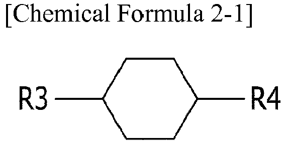


- In Chemical Formulas 2-1 to 2-8, R3 and R4 are independently hydrogen, a C1 to C8 alkyl group, a C2 to C8 alkenyl group, or a C1 to C8 alkoxy group.
- A hydrogen included in R3 and R4 may be substituted with F, a -CH2- group in R3 and R4 may be substituted with -OCH2-, -CF2-, or -OCF2-, and a -CH3 group in R3 and R4 may be substituted with -CF3 or -OCF3.
- Also, in the liquid crystal composition of the liquid crystal layer of the present invention, the compound of Chemical Formula 2-1 to 2-8 may be present in an amount of about 2 wt% to about 40 wt% based on the entire weight of the liquid crystal composition.
- In an embodiment, the liquid crystal composition of the liquid crystal layer may additionally include at least one compound selected from Chemical Formulas 3-1 to 3-12.


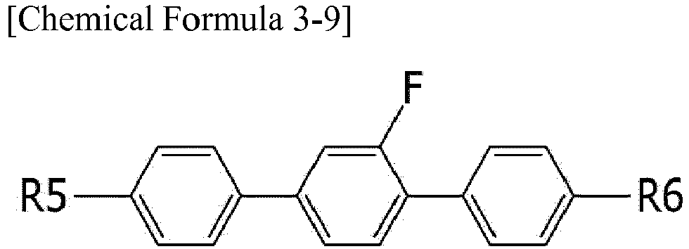


- In Chemical Formulas 3-1 to 3-12, R5 and R6 are independently hydrogen, a C1 to C8 alkyl group, a C2 to C8 alkenyl group, or a C1 to C8 alkoxy group.
- Also, at least one hydrogen included in R5 and R6 may be substituted with fluorine.
- In an embodiment, the compound selected from Chemical Formulas 3-1 to 3-12 may be present in an amount of about 2 wt% to about 30 wt% based on the entire weight of the liquid crystal composition.
- As such, for the liquid crystal display including the compound represented by Chemical Formula 1 within the liquid crystal layer, the rotational viscosity of the liquid crystal layer is low compared to the conventional liquid crystal display, thereby improving the response speed of the liquid crystal display.
- The liquid crystal display having the structure illustrated in
FIG. 1 to FIG. 4 is only one example and the liquid crystal composition according to the present invention may be clearly applied to other liquid crystal displays, without being limited to only the vertical alignment (VA) mode liquid crystal display in which the pixel electrode is positioned in the first display panel and the common electrode is positioned in the second display panel. - While this invention has been described in connection with what is presently considered to be practical embodiments, it is to be understood that the invention is not limited to the disclosed embodiments, but, on the contrary, is intended to cover various modifications and equivalent arrangements included within the scope of the appended claims.
Claims (15)
- A liquid crystal composition comprising one or more compounds represented by Chemical Formula 1:


R1 and R2 are independently a hydrogen, a C1 to C8 alkyl group, a C2 to C8 alkenyl group, or a C1 to C8 alkoxy group. - A liquid crystal composition according to claim 1, wherein:in the compound of Chemical Formula 1, one or more hydrogen in R1 and R2 is substituted with F, one or more -CH2- group in R1 and R2 is substituted with -OCH2-, -CF2-, or -OCF2-, and one or more -CH3 group in R1 and R2 is substituted with -CF3 or -OCF3, and optionally one or more hydrogen in

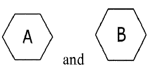
- A liquid crystal composition according to claim 1 or claim 2, wherein:the compound represented by Chemical Formula 1 is at least one compound selected from Chemical Formulas 1-1 to 1-9:


- A liquid crystal composition according to any one of claims 1 to 3, wherein:the compound represented by Chemical Formula 1 is present in an amount of about 1 wt% to about 40 wt% based on the entire weight of the liquid crystal composition.
- A liquid crystal composition according to any one of claims 1 to 4, wherein:the liquid crystal composition further comprises at least one compound selected from Chemical Formulas 2-1 to 2-8:
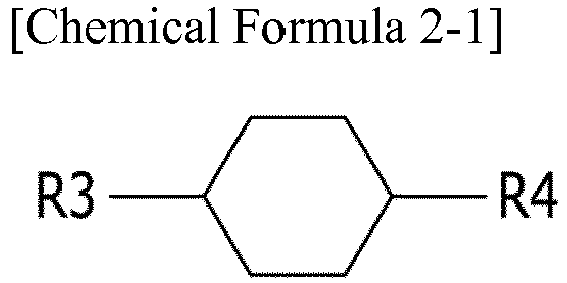

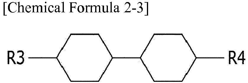
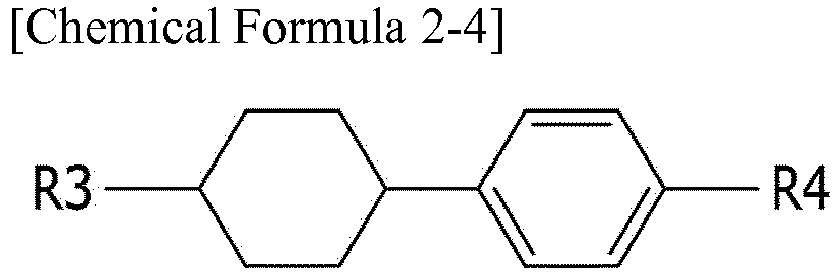


one or more hydrogen in R3 and R4 is substituted with F, one or more -CH2- group in R3 and R4 is substituted with -OCH2-, -CF2-, or -OCF2-, or one or more -CH3 group in R3 and R4 is substituted with -CF3 or -OCF3. - A liquid crystal composition according to claim 5, wherein:wherein the compound selected from Chemical Formulas 2-1 to 2-8 is present in an amount of about 2 wt% to about 40 wt%, based upon the entire weight of the liquid crystal composition.
- A liquid crystal composition according to any one of claims 1 to 6, wherein:the liquid crystal composition further comprises at least one compound selected from Chemical Formulas 3-1 to 3-12:


wherein at least one hydrogen in R5 and R6 is substituted with fluorine. - A liquid crystal composition according to claim 7, wherein:the compound selected from Chemical Formulas 3-1 to 3-12 is present in an amount of about 2 wt% to about 30 wt% based upon the entire liquid crystal composition.
- A liquid crystal display comprising:a first insulation substrate comprising a pixel electrode;a second insulation substrate facing the first insulation substrate and comprising a common electrode; anda liquid crystal layer positioned between the first insulation substrate and the second insulation substrate,wherein the liquid crystal layer comprises a liquid crystal composition comprising one or more compounds represented by Chemical Formula 1:
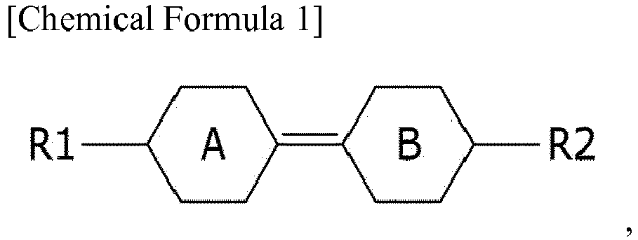

- A liquid crystal display according to claim 9, wherein:in the compound of Chemical Formula 1, one or more hydrogen in R1 and R2 is substituted with F, one or more -CH2- group in R1 and R2 is substituted -OCH2-, -CF2-, or -OCF2-, and one or more -CH3 group in R1 and R2 is substituted with -CF3 or -OCF3; and optionally one or more hydrogen in


- A liquid crystal display according to claim 9 or claim 10, wherein:the compound represented by Chemical Formula 1 is at least one compound selected from Chemical Formulas 1-1 to 1-9:


- A liquid crystal display according to any one of claims 9 to 11, wherein:the compound represented by Chemical Formula 1 is present in an amount of about 1 wt% to about 40 wt% based upon the entire weight of the liquid crystal composition.
- A liquid crystal display according to any one of claims 9 to 12, wherein:the liquid crystal layer further comprises at least one compound selected from Chemical Formulas 2-1 to 2-8:


one or more hydrogen in R3 and R4 is substituted with F, one or more -CH2- group in R3 and R4 is substituted with one among -OCH2-, -CF2-, or -OCF2-, or one or more -CH3 group in R3 and R4 is substituted with -CF3 or -OCF3. - A liquid crystal display according to claim 13, wherein:the compound selected from Chemical Formulas 2-1 to 2-8 is present in an amount of about 2 wt% to about 40 wt% based on the entire weight of the liquid crystal composition.
- A liquid crystal display according to any one of claims 9 to 14, wherein:the liquid crystal layer further comprises at least one compound selected from Chemical Formulas 3-1 to 3-12:


wherein at least one hydrogen in R5 and R6 is substituted with fluorine; and/or
wherein the compound of Chemical Formula 3-1 to 3-12 is present in an amount of about 2 wt% to about 30 wt% based upon the entire weight of the liquid crystal layer.
Applications Claiming Priority (1)
| Application Number | Priority Date | Filing Date | Title |
|---|---|---|---|
| KR1020150076079A KR102388345B1 (en) | 2015-05-29 | 2015-05-29 | Liquid crystal composition and liquid crystal display device comprising the same |
Publications (1)
| Publication Number | Publication Date |
|---|---|
| EP3098286A1 true EP3098286A1 (en) | 2016-11-30 |
Family
ID=56087171
Family Applications (1)
| Application Number | Title | Priority Date | Filing Date |
|---|---|---|---|
| EP16171801.0A Withdrawn EP3098286A1 (en) | 2015-05-29 | 2016-05-27 | Liquid crystal composition and liquid crystal display device comprising the same |
Country Status (5)
| Country | Link |
|---|---|
| US (1) | US10106739B2 (en) |
| EP (1) | EP3098286A1 (en) |
| JP (1) | JP6697325B2 (en) |
| KR (1) | KR102388345B1 (en) |
| CN (1) | CN106190172A (en) |
Citations (4)
| Publication number | Priority date | Publication date | Assignee | Title |
|---|---|---|---|---|
| JPH0769992A (en) * | 1993-08-31 | 1995-03-14 | Hitachi Chem Co Ltd | 4-(4-substituted cyclohexylidene)cyclohexanol derivative and its production |
| US20120261614A1 (en) * | 2011-04-18 | 2012-10-18 | Jnc Petrochemical Corporation | Liquid crystal composition and liquid crystal display device |
| EP2594548A1 (en) * | 2010-07-17 | 2013-05-22 | Organo Science Co. Ltd | Cyclohexane compound and liquid crystal composition containing said compound |
| EP2796922A1 (en) * | 2013-02-21 | 2014-10-29 | DIC Corporation | Liquid crystal display device |
Family Cites Families (14)
| Publication number | Priority date | Publication date | Assignee | Title |
|---|---|---|---|---|
| JPH0687778A (en) * | 1992-09-07 | 1994-03-29 | Hitachi Chem Co Ltd | 4-@(3754/24)4-substituted cyclohexylidene)cyclohexanol derivative and its production |
| WO1997027166A1 (en) * | 1996-01-23 | 1997-07-31 | Chisso Corporation | Benzyl ether derivatives, liquid crystal composition, and liquid crystal display |
| KR100716969B1 (en) | 2003-11-27 | 2007-05-10 | 삼성전자주식회사 | Vertically oriented liquid crystal compound and liquid crystal composition comprising the same |
| DE102005058541A1 (en) * | 2005-12-08 | 2007-06-14 | Merck Patent Gmbh | Liquid crystalline medium |
| KR101490474B1 (en) * | 2008-05-13 | 2015-02-05 | 삼성디스플레이 주식회사 | Liquid crystal composition, liquid crystal display using the same, and manufacturing method thereof |
| CN101928199B (en) * | 2010-08-04 | 2013-02-13 | 烟台万润精细化工股份有限公司 | Divinyl liquid crystal compound and preparation method thereof |
| KR101808888B1 (en) | 2010-10-04 | 2017-12-13 | 제이엔씨 주식회사 | Liquid crystal composition and liquid crystal display element |
| DE102011118210A1 (en) | 2010-11-27 | 2012-05-31 | Merck Patent Gmbh | Liquid crystalline medium |
| TWI550071B (en) | 2011-03-25 | 2016-09-21 | 捷恩智股份有限公司 | Orthoester compound,liquid crystal composition and liquid crystal display device |
| CN102337139A (en) | 2011-08-02 | 2012-02-01 | 江苏和成化学材料有限公司 | Liquid crystal composition and liquid crystal display comprising same |
| KR101921253B1 (en) * | 2012-05-09 | 2018-11-23 | 삼성디스플레이 주식회사 | Liquid crystal display |
| EP2725083B1 (en) * | 2012-10-24 | 2019-03-27 | Merck Patent GmbH | Liquid crystalline medium |
| CN103086848B (en) * | 2013-01-28 | 2014-09-03 | 烟台德润液晶材料有限公司 | Dicyclohexylalkyl ether terminal olefines liquid crystal compound and preparation method thereof |
| CN103998572B (en) * | 2013-03-26 | 2016-02-24 | Dic株式会社 | Liquid crystal composition and liquid crystal display element using same |
-
2015
- 2015-05-29 KR KR1020150076079A patent/KR102388345B1/en active Active
-
2016
- 2016-04-05 US US15/091,371 patent/US10106739B2/en active Active
- 2016-05-26 CN CN201610362632.1A patent/CN106190172A/en active Pending
- 2016-05-27 EP EP16171801.0A patent/EP3098286A1/en not_active Withdrawn
- 2016-05-30 JP JP2016106937A patent/JP6697325B2/en not_active Expired - Fee Related
Patent Citations (4)
| Publication number | Priority date | Publication date | Assignee | Title |
|---|---|---|---|---|
| JPH0769992A (en) * | 1993-08-31 | 1995-03-14 | Hitachi Chem Co Ltd | 4-(4-substituted cyclohexylidene)cyclohexanol derivative and its production |
| EP2594548A1 (en) * | 2010-07-17 | 2013-05-22 | Organo Science Co. Ltd | Cyclohexane compound and liquid crystal composition containing said compound |
| US20120261614A1 (en) * | 2011-04-18 | 2012-10-18 | Jnc Petrochemical Corporation | Liquid crystal composition and liquid crystal display device |
| EP2796922A1 (en) * | 2013-02-21 | 2014-10-29 | DIC Corporation | Liquid crystal display device |
Non-Patent Citations (1)
| Title |
|---|
| REDLOF, HORST; VOEGTLE, FRITZ; PUFF, HEINRICH; REUTER, HANS; WOLLER, PETRA: "Synthese neuer potentiell fluessigkristalliner Verbindungen auf Bicyclohexyliden-Basis - Kristallstruktur des (Z)-3,10-Diphenyldispiro[5.0.5.1]tridecans", JOURNAL OF CHEMICAL RESEARCH, vol. 10, 5 June 1984 (1984-06-05), pages 2910 - 2929, XP008181956, ISSN: 0308-2350 * |
Also Published As
| Publication number | Publication date |
|---|---|
| US10106739B2 (en) | 2018-10-23 |
| KR20160141235A (en) | 2016-12-08 |
| KR102388345B1 (en) | 2022-04-19 |
| CN106190172A (en) | 2016-12-07 |
| JP6697325B2 (en) | 2020-05-20 |
| US20160348002A1 (en) | 2016-12-01 |
| JP2017002285A (en) | 2017-01-05 |
Similar Documents
| Publication | Publication Date | Title |
|---|---|---|
| US10983402B2 (en) | Liquid crystal display device | |
| EP2829909B1 (en) | Curved liquid crystal display and manufacturing method thereof | |
| US9244309B2 (en) | Vertical alignment layer and liquid crystal display including the same | |
| CN101445732B (en) | Liquid crystal composition and liquid crystal display having same | |
| US8153208B2 (en) | Liquid crystal display, a method for manufacturing a liquid crystal display and a liquid crystal composition | |
| EP2921544B1 (en) | Liquid crystal composition and liquid crystal display device including the same | |
| KR20150030526A (en) | Liquid crystal display device | |
| EP3053990B1 (en) | Liquid crystal composition and liquid crystal display including the same | |
| US9416316B2 (en) | Liquid crystal composition and liquid crystal display comprising the same | |
| KR20120117952A (en) | Liquid crystal composition and liquid crystal display comprising the same | |
| KR102272215B1 (en) | Liquid crystal composition, liquid crystal display including the same, and manufacturing method thereof | |
| EP2437111A1 (en) | Liquid crystal panel, method for manufacturing same, and liquid crystal display device | |
| US20170031213A1 (en) | Liquid crystal display | |
| EP3091061A2 (en) | Liquid crystal composition and liquid crystal display including the same | |
| US9422477B2 (en) | Liquid crystal compositon and liquid crystal display including the same | |
| US20170015904A1 (en) | Liquid crystal composition and liquid crystal display including the same | |
| KR102199775B1 (en) | Liquid crystal composition and liquid crystal display comprising the same | |
| EP3098286A1 (en) | Liquid crystal composition and liquid crystal display device comprising the same | |
| US9605205B2 (en) | Liquid crystal composition and liquid crystal display including the same | |
| US9671648B2 (en) | Liquid crystal display and method of manufacturing the same | |
| EP3103856B1 (en) | Liquid crystal composition and liquid crystal display including the same |
Legal Events
| Date | Code | Title | Description |
|---|---|---|---|
| PUAI | Public reference made under article 153(3) epc to a published international application that has entered the european phase |
Free format text: ORIGINAL CODE: 0009012 |
|
| AK | Designated contracting states |
Kind code of ref document: A1 Designated state(s): AL AT BE BG CH CY CZ DE DK EE ES FI FR GB GR HR HU IE IS IT LI LT LU LV MC MK MT NL NO PL PT RO RS SE SI SK SM TR |
|
| AX | Request for extension of the european patent |
Extension state: BA ME |
|
| 17P | Request for examination filed |
Effective date: 20170308 |
|
| RBV | Designated contracting states (corrected) |
Designated state(s): AL AT BE BG CH CY CZ DE DK EE ES FI FR GB GR HR HU IE IS IT LI LT LU LV MC MK MT NL NO PL PT RO RS SE SI SK SM TR |
|
| 17Q | First examination report despatched |
Effective date: 20180803 |
|
| RIC1 | Information provided on ipc code assigned before grant |
Ipc: C09K 19/12 20060101ALI20190509BHEP Ipc: C07C 23/18 20060101ALI20190509BHEP Ipc: C07C 43/188 20060101ALI20190509BHEP Ipc: C07C 43/192 20060101ALI20190509BHEP Ipc: C09K 19/30 20060101ALI20190509BHEP Ipc: C07D 309/04 20060101AFI20190509BHEP Ipc: G02F 1/1343 20060101ALI20190509BHEP Ipc: C09K 19/34 20060101ALI20190509BHEP Ipc: C07C 22/00 20060101ALI20190509BHEP Ipc: C09K 19/06 20060101ALI20190509BHEP Ipc: C07C 13/28 20060101ALI20190509BHEP |
|
| STAA | Information on the status of an ep patent application or granted ep patent |
Free format text: STATUS: THE APPLICATION IS DEEMED TO BE WITHDRAWN |
|
| 18D | Application deemed to be withdrawn |
Effective date: 20191015 |