EP3093994A2 - Apparatus for performing multi-loop power control in an electronic device with aid of analog compensation and duty cycle selection, and associated method - Google Patents
Apparatus for performing multi-loop power control in an electronic device with aid of analog compensation and duty cycle selection, and associated method Download PDFInfo
- Publication number
- EP3093994A2 EP3093994A2 EP15193637.4A EP15193637A EP3093994A2 EP 3093994 A2 EP3093994 A2 EP 3093994A2 EP 15193637 A EP15193637 A EP 15193637A EP 3093994 A2 EP3093994 A2 EP 3093994A2
- Authority
- EP
- European Patent Office
- Prior art keywords
- signal
- amplifier
- electronic device
- power control
- error signal
- Prior art date
- Legal status (The legal status is an assumption and is not a legal conclusion. Google has not performed a legal analysis and makes no representation as to the accuracy of the status listed.)
- Granted
Links
Images


Classifications
-
- G—PHYSICS
- G05—CONTROLLING; REGULATING
- G05F—SYSTEMS FOR REGULATING ELECTRIC OR MAGNETIC VARIABLES
- G05F1/00—Automatic systems in which deviations of an electric quantity from one or more predetermined values are detected at the output of the system and fed back to a device within the system to restore the detected quantity to its predetermined value or values, i.e. retroactive systems
- G05F1/66—Regulating electric power
-
- H—ELECTRICITY
- H02—GENERATION; CONVERSION OR DISTRIBUTION OF ELECTRIC POWER
- H02J—ELECTRIC POWER NETWORKS; CIRCUIT ARRANGEMENTS OR SYSTEMS FOR SUPPLYING OR DISTRIBUTING ELECTRIC POWER; SYSTEMS FOR STORING ELECTRIC ENERGY
- H02J7/00—Circuit arrangements for charging or discharging batteries or for supplying loads from batteries
- H02J7/855—Circuit arrangements for charging or discharging batteries or for supplying loads from batteries with circuits adapted for supplying loads from the battery
-
- H—ELECTRICITY
- H02—GENERATION; CONVERSION OR DISTRIBUTION OF ELECTRIC POWER
- H02J—ELECTRIC POWER NETWORKS; CIRCUIT ARRANGEMENTS OR SYSTEMS FOR SUPPLYING OR DISTRIBUTING ELECTRIC POWER; SYSTEMS FOR STORING ELECTRIC ENERGY
- H02J7/00—Circuit arrangements for charging or discharging batteries or for supplying loads from batteries
-
- H—ELECTRICITY
- H02—GENERATION; CONVERSION OR DISTRIBUTION OF ELECTRIC POWER
- H02M—APPARATUS FOR CONVERSION BETWEEN AC AND AC, BETWEEN AC AND DC, OR BETWEEN DC AND DC, AND FOR USE WITH MAINS OR SIMILAR POWER SUPPLY SYSTEMS; CONVERSION OF DC OR AC INPUT POWER INTO SURGE OUTPUT POWER; CONTROL OR REGULATION THEREOF
- H02M3/00—Conversion of DC power input into DC power output
- H02M3/02—Conversion of DC power input into DC power output without intermediate conversion into AC
- H02M3/04—Conversion of DC power input into DC power output without intermediate conversion into AC by static converters
- H02M3/10—Conversion of DC power input into DC power output without intermediate conversion into AC by static converters using discharge tubes with control electrode or semiconductor devices with control electrode
- H02M3/145—Conversion of DC power input into DC power output without intermediate conversion into AC by static converters using discharge tubes with control electrode or semiconductor devices with control electrode using devices of a triode or transistor type requiring continuous application of a control signal
- H02M3/155—Conversion of DC power input into DC power output without intermediate conversion into AC by static converters using discharge tubes with control electrode or semiconductor devices with control electrode using devices of a triode or transistor type requiring continuous application of a control signal using semiconductor devices only
- H02M3/156—Conversion of DC power input into DC power output without intermediate conversion into AC by static converters using discharge tubes with control electrode or semiconductor devices with control electrode using devices of a triode or transistor type requiring continuous application of a control signal using semiconductor devices only with automatic control of output voltage or current, e.g. switching regulators
- H02M3/158—Conversion of DC power input into DC power output without intermediate conversion into AC by static converters using discharge tubes with control electrode or semiconductor devices with control electrode using devices of a triode or transistor type requiring continuous application of a control signal using semiconductor devices only with automatic control of output voltage or current, e.g. switching regulators including plural semiconductor devices as final control devices for a single load
-
- H—ELECTRICITY
- H03—ELECTRONIC CIRCUITRY
- H03F—AMPLIFIERS
- H03F3/00—Amplifiers with only discharge tubes or only semiconductor devices as amplifying elements
- H03F3/45—Differential amplifiers
- H03F3/45071—Differential amplifiers with semiconductor devices only
- H03F3/45076—Differential amplifiers with semiconductor devices only characterised by the way of implementation of the active amplifying circuit in the differential amplifier
- H03F3/45179—Differential amplifiers with semiconductor devices only characterised by the way of implementation of the active amplifying circuit in the differential amplifier using MOSFET transistors as the active amplifying circuit
-
- H—ELECTRICITY
- H04—ELECTRIC COMMUNICATION TECHNIQUE
- H04B—TRANSMISSION
- H04B1/00—Details of transmission systems, not covered by a single one of groups H04B3/00 - H04B13/00; Details of transmission systems not characterised by the medium used for transmission
- H04B1/38—Transceivers, i.e. devices in which transmitter and receiver form a structural unit and in which at least one part is used for functions of transmitting and receiving
- H04B1/3827—Portable transceivers
-
- H—ELECTRICITY
- H02—GENERATION; CONVERSION OR DISTRIBUTION OF ELECTRIC POWER
- H02J—ELECTRIC POWER NETWORKS; CIRCUIT ARRANGEMENTS OR SYSTEMS FOR SUPPLYING OR DISTRIBUTING ELECTRIC POWER; SYSTEMS FOR STORING ELECTRIC ENERGY
- H02J2207/00—Details of circuit arrangements for charging or discharging batteries or supplying loads from batteries
- H02J2207/20—Charging or discharging characterised by the power electronics converter
-
- H—ELECTRICITY
- H02—GENERATION; CONVERSION OR DISTRIBUTION OF ELECTRIC POWER
- H02J—ELECTRIC POWER NETWORKS; CIRCUIT ARRANGEMENTS OR SYSTEMS FOR SUPPLYING OR DISTRIBUTING ELECTRIC POWER; SYSTEMS FOR STORING ELECTRIC ENERGY
- H02J7/00—Circuit arrangements for charging or discharging batteries or for supplying loads from batteries
- H02J7/90—Regulation of charging or discharging current or voltage
-
- H—ELECTRICITY
- H03—ELECTRONIC CIRCUITRY
- H03F—AMPLIFIERS
- H03F2200/00—Indexing scheme relating to amplifiers
- H03F2200/351—Pulse width modulation being used in an amplifying circuit
-
- H—ELECTRICITY
- H03—ELECTRONIC CIRCUITRY
- H03F—AMPLIFIERS
- H03F2200/00—Indexing scheme relating to amplifiers
- H03F2200/471—Indexing scheme relating to amplifiers the voltage being sensed
-
- H—ELECTRICITY
- H03—ELECTRONIC CIRCUITRY
- H03F—AMPLIFIERS
- H03F2203/00—Indexing scheme relating to amplifiers with only discharge tubes or only semiconductor devices as amplifying elements covered by H03F3/00
- H03F2203/45—Indexing scheme relating to differential amplifiers
- H03F2203/45116—Feedback coupled to the input of the differential amplifier
-
- H—ELECTRICITY
- H03—ELECTRONIC CIRCUITRY
- H03K—PULSE TECHNIQUE
- H03K7/00—Modulating pulses with a continuously-variable modulating signal
- H03K7/08—Duration or width modulation ; Duty cycle modulation
Definitions
- the present invention relates to apparatus for performing multi-loop power control in an electronic device according to the pre-characterizing clauses of claims 1 and 11, and associated operational method thereof.
- the present invention aims at providing an apparatus for performing multi-loop power control in an electronic device, and an associated method, to keep high stability of the electronic device in each of various situations and/or to reduce the charging time of a charger within the electronic device.
- the disclosure features an apparatus for performing multi-loop power control in an electronic device, where the apparatus may comprise at least one portion (e.g. a portion or all) of the electronic device.
- the apparatus may comprise a first amplifier that is positioned in a first feedback loop of the electronic device and coupled to a power control terminal of the electronic device, a second amplifier that is positioned in a second feedback loop of the electronic device and coupled to the power control terminal, and a compensation circuit that is coupled to the first amplifier and the second amplifier.
- the first amplifier is arranged for selectively outputting a first error signal toward the power control terminal.
- the second amplifier is arranged for selectively outputting a second error signal toward the power control terminal.
- the compensation circuit is arranged for detecting the first error signal to generate a compensation signal corresponding to the first error signal and applying the compensation signal to the second error signal, to perform power control of the electronic device.
- the disclosure features a method for performing multi-loop power control in an electronic device, such as an operational method of the above apparatus.
- this method such as the operational method of the above apparatus may comprise: utilizing the first amplifier to selectively output the first error signal toward the power control terminal; utilizing the second amplifier to selectively output the second error signal toward the power control terminal; and applying the compensation signal corresponding to the first error signal to the second error signal, to perform power control of the electronic device.
- the disclosure features an apparatus for performing multi-loop power control in an electronic device, where the apparatus may comprise at least one portion (e.g. a portion or all) of the electronic device.
- the apparatus may comprise a first amplifier that is positioned in a first feedback loop of the electronic device, a second amplifier that is positioned in a second feedback loop of the electronic device, and a selection control circuit that is coupled to the first amplifier and the second amplifier.
- the first amplifier is arranged for selectively outputting a first error signal.
- the second amplifier is arranged for selectively outputting a second error signal.
- the selection control circuit is arranged for detecting a first pulse width modulation (PWM) signal corresponding to the first error signal and a second PWM signal corresponding to the second error signal to generate at least one detection result, and dynamically selecting one of the first PWM signal and the second PWM signal as a resultant PWM signal according to the at least one detection result, to perform power control of the electronic device.
- PWM pulse width modulation
- the disclosure features a method for performing multi-loop power control in an electronic device, such as an operational method of the above apparatus.
- this method such as the operational method of the above apparatus may comprise: utilizing the first amplifier to selectively output the first error signal; utilizing the second amplifier to selectively output the second error signal; and detecting the first PWM signal corresponding to the first error signal and the second PWM signal corresponding to the second error signal to generate the at least one detection result, and dynamically selecting the one of the first PWM signal and the second PWM signal as the resultant PWM signal according to the at least one detection result, to perform power control of the electronic device.
- the present invention apparatus and method can reduce the overlap effect (e.g. a non-sharp transition boundary effect) from an overlap between activation time periods of multiple feedback loops within the electronic device, and keep high stability of the electronic device in each of various situations. For example, in a situation where the multiple feedback loops are utilized for performing charging control of a charger within the electronic device in different charging phases, respectively, the present invention apparatus and method can reduce the charging time of the charger.
- the overlap effect e.g. a non-sharp transition boundary effect
- FIG. 1 illustrates an overlap effect from an overlap between activation time periods of multiple feedback loops of a conventional charger system according to the related art, where the horizontal axis represents the charging time, and the vertical axis represents the charging current.
- CC constant current
- CV constant voltage
- FIG. 2 illustrates another overlap effect from an overlap between activation time periods of multiple feedback loops of a conventional charger system according to the related art, where the horizontal axis represents the charging time, and the vertical axis represents the charging current.
- IBAT in FIG. 2 for brevity
- ICL ICL phase
- FIG. 2 illustrates another overlap effect from an overlap between activation time periods of multiple feedback loops of a conventional charger system according to the related art, where the horizontal axis represents the charging time, and the vertical axis represents the charging current.
- FIG. 3 is a diagram of an apparatus 100 for performing multi-loop power control in an electronic device according to an embodiment of the present invention, where the apparatus 100 may comprise at least one portion of the electronic device.
- the apparatus 100 may comprise a portion of the electronic device mentioned above, and more particularly, can be at least one hardware circuit such as at least one integrated circuit (IC) within the electronic device and associated circuits thereof.
- the apparatus 100 can be the whole of the electronic device mentioned above.
- the apparatus 100 may comprise a system comprising the electronic device mentioned above (e.g. a wireless communications system comprising the electronic device). Examples of the electronic device may include, but not limited to, a multifunctional mobile phone, a tablet, and a laptop computer.
- the apparatus 100 may comprise a first amplifier 112 (labeled “AMP” in FIG. 1 , for brevity) that is positioned in a first feedback loop 110 of the electronic device and coupled to a power control terminal 142 of the electronic device, a second amplifier 122 (labeled “AMP” in FIG. 1 , for brevity) that is positioned in a second feedback loop 120 of the electronic device and coupled to the power control terminal 142, and a compensation circuit 130 that is coupled to the first amplifier 112 and the second amplifier 122.
- AMP first amplifier 112
- AMP second amplifier
- the first feedback loop 110 may further comprise a diode coupled between the first amplifier 112 and the power control terminal 142 for controlling the current direction of a current between the first amplifier 112 and the power control terminal 142
- the second feedback loop 120 may further comprise a diode coupled between the second amplifier 122 and the power control terminal 142 for controlling the current direction of a current between the second amplifier 122 and the power control terminal 142.
- the power control terminal 142 may be positioned in a power control circuit 140 within the electronic device.
- the power control circuit 140 may comprise a current source coupled to the power control terminal 142, and may comprise a transistor such as a Metal Oxide Semiconductor Field Effect Transistor (MOSFET).
- MOSFET Metal Oxide Semiconductor Field Effect Transistor
- the first amplifier 112 is arranged for selectively outputting a first error signal toward the power control terminal 142.
- the second amplifier 122 is arranged for selectively outputting a second error signal toward the power control terminal 142.
- the compensation circuit 130 is arranged for detecting the first error signal to generate a compensation signal corresponding to the first error signal and applying the compensation signal to the second error signal, to perform power control of the electronic device.
- the power control terminal 142 may receive the first error signal as a feedback of the first feedback loop 110, to perform power control of the electronic device, and the power control terminal 142 may receive the second error signal as a feedback of the second feedback loop 120, to perform power control of the electronic device.
- the first amplifier 112 may have a first monitoring input terminal (e.g. a positive input terminal labeled "+” in this embodiment) for inputting a first monitoring signal FB1 and a first reference input terminal (e.g. a negative input terminal labeled "-'' in this embodiment) for inputting a first reference signal REF1
- the second amplifier 122 may have a second monitoring input terminal (e.g. a positive input terminal labeled "+” in this embodiment) for inputting a second monitoring signal FB2 and a second reference input terminal (e.g. a negative input terminal labeled "-" in this embodiment) for inputting a second reference signal REF2.
- the electronic device may utilize the first feedback loop 110 to monitor the first monitoring signal FB1 according to the first reference signal REF1, to perform power control of the electronic device.
- the electronic device may utilize the second feedback loop 120 to monitor the second monitoring signal FB2 according to the second reference signal REF2, to perform power control of the electronic device.
- the compensation signal may be equivalent to a product of the first error signal and a predetermined factor, where the predetermined factor is a non-zero factor.
- the predetermined factor may be equal to 100%.
- the strength of the compensation signal may be equal to that of the first error signal.
- the predetermined factor may be equal to any other predetermined value.
- the compensation circuit 130 may apply the compensation signal to the second error signal, to reduce influence of the first feedback loop 110 on the second feedback loop 120 during a time period in which the electronic device switches from power control of the second feedback loop 120 to power control of the first feedback loop 110.
- the first feedback loop 110 may be utilized for performing charging control in a constant voltage control phase such as the constant voltage (CV) phase mentioned above
- the second feedback loop 120 may be utilized for performing charging control in a constant current control phase such as the constant current (CC) phase mentioned above.
- the compensation circuit 130 may apply the compensation signal to the second error signal, to reduce influence of the first feedback loop 110 on the second feedback loop 120 during the time period in which the electronic device switches from the constant current control of the second feedback loop 120 to the constant voltage control of the first feedback loop 110.
- the compensation circuit 130 may apply the compensation signal to the second error signal, to remove influence of the first feedback loop 110 on the second feedback loop 120 during the time period in which the electronic device switches from the power control of the second feedback loop 120 to the power control of the first feedback loop 110.
- the compensation circuit 130 may comprise a detector that is coupled to the first amplifier 112, and may further comprise a compensator that is coupled to the detector and the second amplifier 122.
- the detector may be arranged for detecting the first error signal to generate a detection signal
- the compensator may be arranged for generating the compensation signal according to the detection signal and applying the compensation signal to the second error signal.
- the compensator may be arranged for applying a derivative of the compensation signal to the second error signal.
- At least one of the first amplifier 112 and the second amplifier 122 may be implemented with various types of circuits.
- at least one of the first amplifier 112 and the second amplifier 122 may comprise an output transconductance amplifier (OTA), where the OTA may be arranged for converting a voltage difference into a current error signal.
- OTA output transconductance amplifier
- one of the first amplifier 112 and the second amplifier 122, or each of the first amplifier 112 and the second amplifier 122) may comprise a current source, where this current source may be arranged for converting a current difference into a current error signal.
- at least one of the first amplifier 112 and the second amplifier 122 e.g. one of the first amplifier 112 and the second amplifier 122, or each of the first amplifier 112 and the second amplifier 122 may comprise an operational amplifier (OPAMP) and a voltage-to-current converter, where the OPAMP may be arranged for converting a voltage difference into a voltage error signal, and the voltage-to-current converter may be arranged for converting the voltage error signal into a current error signal.
- OPAMP operational amplifier
- the OPAMP may be arranged for converting a voltage difference into a voltage error signal
- the voltage-to-current converter may be arranged for converting the voltage error signal into a current error signal.
- the apparatus 100 may be applied to various types of power control circuits corresponding to various kinds of scenarios.
- the power control terminal 142 may be a control terminal of a charger within the electronic device, where the electronic device may selectively utilize the first feedback loop 110 to monitor a voltage of a battery charged by the charger in a constant voltage control phase, and may selectively utilize the second feedback loop 120 to monitor a charging current of the battery in a constant current control phase.
- the power control terminal 142 may be a control terminal of a regulating circuit within the electronic device, where the electronic device may selectively utilize the first feedback loop 110 to monitor an output voltage of the regulating circuit, and may selectively utilize the second feedback loop 120 to monitor a current passing through the regulating circuit. Additionally, in some of these embodiments, the power control terminal 142 may be a control terminal of a regulating circuit within the electronic device, where the electronic device may selectively utilize the first feedback loop 110 to monitor an output voltage that the regulating circuit applied to a load, and may selectively utilize the second feedback loop 120 to monitor a current that the regulating circuit draws from a power source of the regulating circuit.
- FIG. 4 illustrates an overlap effect removal scheme involved with the apparatus 100 shown in FIG. 3 according to an embodiment of the present invention.
- each of the first amplifier 112 and the second amplifier 122 may comprise an OTA such as that mentioned above.
- the power control terminal 142 may be the control terminal of the charger within the electronic device, where the electronic device may selectively utilize the first feedback loop 110 to monitor the voltage of the battery charged by the charger in the constant voltage control phase, and may selectively utilize the second feedback loop 120 to monitor the charging current of the battery in the constant current control phase.
- the relationship between the charging current and the charging time can be expressed with the curve 210.
- the compensation signal may be intentionally or unintentionally designed to be insufficient for correcting the overlap effect shown in FIG. 1 .
- the overlap effect removal scheme shown in FIG. 4 becomes an overlap effect reduction scheme in these embodiments.
- similar descriptions for these embodiments are not repeated in detail here.
- FIG. 5 illustrates an overlap effect removal scheme involved with the apparatus 100 shown in FIG. 3 according to another embodiment of the present invention.
- each of the first amplifier 112 and the second amplifier 122 may comprise an OTA such as that mentioned above.
- the power control terminal 142 may be the control terminal of the charger within the electronic device. Additionally, the relationship between the charging current and the charging time can be expressed with the curve 220.
- the two transitions are close to each other in the curve 210, rather than being far from each other.
- the overlap effect can be removed.
- the charging time of the charger of this embodiment is reduced since the overlap effect shown in FIG. 2 is removed.
- the horizontal line EOC represents the end-of-charging current
- the speed up time shown in FIG. 5 indicates that the charging time of the charger of this embodiment is shorter.
- the compensation signal may be intentionally or unintentionally designed to be insufficient for correcting the overlap effect shown in FIG. 2 .
- the overlap effect removal scheme shown in FIG. 5 becomes an overlap effect reduction scheme in these embodiments.
- similar descriptions for these embodiments are not repeated in detail here.
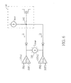
- FIG. 6 illustrates a control scheme involved with the apparatus 100 shown in FIG. 3 according to an embodiment of the present invention.
- each of the first amplifier 112 and the second amplifier 122 may comprise an OTA such as that mentioned above.
- the first amplifier 112 can be implemented with an OTA OTA1
- the second amplifier 122 can be implemented with an OTA OTA2.
- the compensation circuit 130 may comprise a current source 330 generating a compensation current I COMP corresponding to the detection signal mentioned above, where the compensation current I COMP can be taken as an example of the compensation signal mentioned above, the current I1 can be taken as an example of the first error signal, and the current I2 can be taken as an example of the second error signal.
- the current I BIAS of the current source in the power control circuit 140 may be equal to the summation of the current I1 corresponding to the first feedback loop 110 and the current I2 corresponding to the second feedback loop 120.
- the power control terminal 142 may be the control terminal of the charger within the electronic device.
- the apparatus 100 may control the compensation current I COMP to be equal to the current I1, to make the output current of the OTA OTA2 be equal to the current I BIAS , thereby the overlap effect can be removed.
- the compensation current I COMP may be equal to the current I1
- the output current of the OTA OTA2 may be equal to the current I BIAS , thereby the overlap effect can be removed.
- FIG. 7 illustrates a control scheme involved with the apparatus 100 shown in FIG. 3 according to another embodiment of the present invention.
- each of the first amplifier 112 and the second amplifier 122 may comprise an OTA such as that mentioned above.
- the first amplifier 112 can be implemented with the OTA OTA1
- the second amplifier 122 can be implemented with the OTA OTA2.
- the current detector 432 and the current compensator can be taken as examples of the detector and the compensator mentioned in some embodiments described above, respectively.
- the power control terminal 142 may be the control terminal of the charger within the electronic device. For brevity, similar descriptions for this embodiment are not repeated in detail here.
- FIG. 8 illustrates a control scheme involved with the apparatus 100 shown in FIG. 3 according to another embodiment of the present invention.
- each of the first amplifier 112 and the second amplifier 122 may comprise an OPAMP such as that mentioned above.
- the first amplifier 112 can be implemented with an OPAMP shown around the upper left corner of FIG. 8 , where the notation "CV" indicates that the first feedback loop 110 comprising this OPAMP can be utilized for performing charging control in the constant voltage control phase such as the constant voltage (CV) phase mentioned above.
- the second amplifier 122 can be implemented with an OPAMP shown around the lower left corner of FIG. 8 , where the notation "CC" indicates that the second feedback loop 120 comprising this OPAMP can be utilized for performing charging control in the constant current control phase such as the constant current (CC) phase mentioned above.
- the compensation circuit 130 may comprise some transistors such as the MOSFETs MA, MB, MC, MD, and NX, and may further comprises some current sources generating the currents I A , I B , and I C , respectively.
- some associated currents I CV , I CC , I CVO , I CCO , and I CVX are illustrated, where the current I CVX can be taken as an example of the compensation signal mentioned above, the current I CVO can be taken as an example of the first error signal, and the current I CCO can be taken as an example of the second error signal.
- the terminal COMP can be taken as an example of the power control terminal 142. For brevity, similar descriptions for this embodiment are not repeated in detail here.
- a method for performing multi-loop power control in an electronic device such as an operational method of the apparatus 100 shown in FIG. 1
- this method such as the operational method of the apparatus 100 may comprise: utilizing the first amplifier 112 to selectively output the first error signal toward the power control terminal 142; utilizing the second amplifier 122 to selectively output the second error signal toward the power control terminal 142; and applying the compensation signal corresponding to the first error signal to the second error signal, to perform power control of the electronic device.
- the apparatus 600 and the method thereof can reduce the overlap effect (e.g. the non-sharp transition boundary effect) from an overlap between activation time periods of multiple feedback loops within the electronic device. For brevity, similar descriptions for these embodiments are not repeated in detail here.
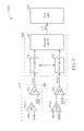
- FIG. 9 is a diagram of an apparatus 600 for performing multi-loop power control in an electronic device (e.g. the electronic device mentioned in the embodiment shown in FIG. 1 ) according to another embodiment of the present invention, where the apparatus 600 may comprise at least one portion of this electronic device.
- the apparatus 600 may comprise a portion of the electronic device mentioned above, and more particularly, can be at least one hardware circuit such as at least one IC within the electronic device and associated circuits thereof.
- the apparatus 600 can be the whole of the electronic device mentioned above.
- the apparatus 600 may comprise a system comprising the electronic device mentioned above (e.g. a wireless communications system comprising the electronic device). Examples of the electronic device may include, but not limited to, a multifunctional mobile phone, a tablet, and a laptop computer.
- the apparatus 600 may comprise a first amplifier that is positioned in a first feedback loop 610 of the electronic device, such as the first amplifier 112 positioned in the first feedback loop 110, and may further comprise a second amplifier that is positioned in a second feedback loop 620 of the electronic device, such as the second amplifier 122 positioned in the second feedback loop 120.
- a power control terminal such as the power control terminal 142.
- the apparatus 600 may comprise the OTA OTA1 and a comparator 614 that are positioned in the first feedback loop 610, and may comprise the OTA OTA2 and a comparator 624 that are positioned in the second feedback loop 620, where the OTA OTA1 can be taken as an example of the first amplifier of the apparatus 600, and the OTA OTA2 can be taken as an example of the second amplifier of the apparatus 600.
- the apparatus 600 may further comprise a selection control circuit 630 that is coupled to the first amplifier and the second amplifier of the apparatus 600 (more particularly, coupled to the OTAs OTA1 and OTA2 through the comparators 614 and 624, respectively), and a pulse width modulation (PWM) logic 640 (which can also be referred to as the PWM logic circuit).
- the selection control circuit 630 may comprise a plurality of count circuits such as two count circuits 631 and 632, and may further comprise a decision circuit 634 that is coupled to the plurality of count circuits such as the two count circuits 631 and 632.
- the first amplifier of the apparatus 600 may be arranged for selectively outputting a first error signal such as that mentioned above
- the second amplifier of the apparatus 600 e.g. the OTA OTA2
- the comparator 614 may compare the first error signal with a first periodic ramp signal to generate a first PWM signal duty1 corresponding to the first error signal
- the comparator 624 may compare the second error signal with a second periodic ramp signal to generate a second PWM signal duty2 corresponding to the second error signal.
- the first periodic ramp signal and the second periodic ramp signal are illustrated with some ramp waveforms, respectively. As shown in FIG.
- the selection control circuit 130 is arranged for detecting the first PWM signal duty1 and the second PWM signal duty2 to generate at least one detection result, and dynamically selecting one of the first PWM signal duty1 and the second PWM signal duty2 as a resultant PWM signal (labeled "true duty” in FIG. 9 , for better comprehension) according to the aforementioned at least one detection result, to perform power control of the electronic device.
- the count circuits 631 and 632 may count the first PWM signal duty1 and the second PWM signal duty2 to generate a first count result and a second count result, respectively, where the aforementioned at least one detection result may comprise the first count result and the second count result (e.g. the first count result and the second count result can be taken as examples of the aforementioned at least one detection result).
- the decision circuit 634 may determine whether one pulse within a pulse of the first PWM signal duty1 and a pulse of the second PWM signal duty2 appears earlier than another pulse within the pulse of the first PWM signal duty1 and the pulse of the second PWM signal duty2, in order to dynamically select the aforementioned one of the first PWM signal duty1 and the second PWM signal duty2 as the resultant PWM signal.
- the PWM logic 640 may perform power control according to the resultant PWM signal that is dynamically selected from the first PWM signal duty1 and the second PWM signal duty2 by the selection control circuit 130.
- the selection control circuit 630 may monitor a first duty cycle of the first PWM signal duty1 and a second duty cycle of the second PWM signal duty2, respectively, to generate the aforementioned at least one detection result.
- the aforementioned at least one detection result may comprise statistics data, such as the statistics data related to at least one of the first duty cycle and the second duty cycle.
- FIG. 10 illustrates a control scheme involved with the apparatus 600 shown in FIG. 9 according to an embodiment of the present invention.
- the decision circuit 634 may determine that the pulse of the second PWM signal duty2 appears earlier than the pulse of the first PWM signal duty1.
- the decision circuit 634 may determine that the pulse of the first PWM signal duty1 appears earlier than the pulse of the second PWM signal duty2.
- the decision circuit 634 may detect different situations such as those shown in FIG. 10 at different time points, respectively. For example, based on whether the situations (a) or (b) are detected and/or the occurrence patterns of the situations (a) and (b), the decision circuit 634 may dynamically select the aforementioned one of the first PWM signal duty1 and the second PWM signal duty2 as the resultant PWM signal.
- the statistics data may comprise whether one situation within the situations (a) and (b) has been continuously detected for A1 times, where the notation "A1" may represent a positive integer.
- the first PWM signal duty1 is originally selected as the resultant PWM signal by the decision circuit 634 at a time point.
- the decision circuit 634 may select the second PWM signal duty2 as the resultant PWM signal at another time point.
- the second PWM signal duty2 is originally selected as the resultant PWM signal by the decision circuit 634 at a time point.
- the decision circuit 634 may select the first PWM signal duty1 as the resultant PWM signal at another time point.
- the statistics data may comprise whether the occurrence pattern of the situation (a) complies with a predetermined pattern and/or whether the occurrence pattern of the situation (b) complies with a predetermined pattern.
- the notation "N2" represents a positive value that is less than or equal to one, and that the summation of the number of occurrence of the situation (a) and the number of occurrence of the situation (b) is equal to A2, where the notation "A2" may represent a positive integer.
- the first PWM signal duty1 is originally selected as the resultant PWM signal by the decision circuit 634 at a time point.
- the decision circuit 634 may select the second PWM signal duty2 as the resultant PWM signal at another time point.
- the second PWM signal duty2 is originally selected as the resultant PWM signal by the decision circuit 634 at a time point.
- the decision circuit 634 may select the first PWM signal duty1 as the resultant PWM signal at another time point. This is for illustrative purposes only, and is not meant to be a limitation of the present invention.
- the decision circuit 634 may select the second PWM signal duty2 as the resultant PWM signal at another time point.
- the decision circuit 634 may select the first PWM signal duty1 as the resultant PWM signal at another time point.
- the percentage of 50% in the aforementioned (50% * A3) times may vary. For example, the percentage of 50% may be increased. In another example, the percentage of 50% may be replaced by 100%. According some embodiments, the percentage of 50% in the aforementioned (50% * A3) times may be replaced by a predetermined programmable ratio.
- a method for performing multi-loop power control in an electronic device such as an operational method of the apparatus 600 shown in FIG. 9
- this method such as the operational method of the apparatus 600 may comprise: utilizing the first amplifier to selectively output the first error signal; utilizing the second amplifier to selectively output the second error signal; and detecting the first PWM signal duty1 corresponding to the first error signal and the second PWM signal duty2 corresponding to the second error signal to generate the at least one detection result, and dynamically selecting the one of the first PWM signal duty1 and the second PWM signal duty2 as the resultant PWM signal according to the at least one detection result, to perform power control of the electronic device.
- the apparatus 600 and the method thereof can keep high stability of the electronic device in each of various situations. For brevity, similar descriptions for these embodiments are not repeated in detail here.
Landscapes
- Engineering & Computer Science (AREA)
- Power Engineering (AREA)
- Computer Networks & Wireless Communication (AREA)
- Signal Processing (AREA)
- Physics & Mathematics (AREA)
- Electromagnetism (AREA)
- General Physics & Mathematics (AREA)
- Radar, Positioning & Navigation (AREA)
- Automation & Control Theory (AREA)
- Amplifiers (AREA)
- Dc-Dc Converters (AREA)
Abstract
Description
- The present invention relates to apparatus for performing multi-loop power control in an electronic device according to the pre-characterizing clauses of
claims - According to the related art, there are many problems in the conventional charger systems. For example, overlap effects between multiple feedback loops of the conventional charger systems may degrade the performance of the conventional charger systems, and each of the conventional charger systems cannot guarantee high stability in each of various situations. Thus, how to reduce (e.g. to remove) the overlap effects in order to guarantee the overall performance of the whole system has become an important issue to be solved.
- This in mind, the present invention aims at providing an apparatus for performing multi-loop power control in an electronic device, and an associated method, to keep high stability of the electronic device in each of various situations and/or to reduce the charging time of a charger within the electronic device.
- This is achieved by apparatus for performing multi-loop power control in an electronic device according to the pre-characterizing clauses of
claims - In one aspect, the disclosure features an apparatus for performing multi-loop power control in an electronic device, where the apparatus may comprise at least one portion (e.g. a portion or all) of the electronic device. For example, the apparatus may comprise a first amplifier that is positioned in a first feedback loop of the electronic device and coupled to a power control terminal of the electronic device, a second amplifier that is positioned in a second feedback loop of the electronic device and coupled to the power control terminal, and a compensation circuit that is coupled to the first amplifier and the second amplifier. The first amplifier is arranged for selectively outputting a first error signal toward the power control terminal. In addition, the second amplifier is arranged for selectively outputting a second error signal toward the power control terminal. Additionally, the compensation circuit is arranged for detecting the first error signal to generate a compensation signal corresponding to the first error signal and applying the compensation signal to the second error signal, to perform power control of the electronic device.
- In one aspect, the disclosure features a method for performing multi-loop power control in an electronic device, such as an operational method of the above apparatus. For example, this method such as the operational method of the above apparatus may comprise: utilizing the first amplifier to selectively output the first error signal toward the power control terminal; utilizing the second amplifier to selectively output the second error signal toward the power control terminal; and applying the compensation signal corresponding to the first error signal to the second error signal, to perform power control of the electronic device.
- In one aspect, the disclosure features an apparatus for performing multi-loop power control in an electronic device, where the apparatus may comprise at least one portion (e.g. a portion or all) of the electronic device. For example, the apparatus may comprise a first amplifier that is positioned in a first feedback loop of the electronic device, a second amplifier that is positioned in a second feedback loop of the electronic device, and a selection control circuit that is coupled to the first amplifier and the second amplifier. The first amplifier is arranged for selectively outputting a first error signal. In addition, the second amplifier is arranged for selectively outputting a second error signal. Additionally, the selection control circuit is arranged for detecting a first pulse width modulation (PWM) signal corresponding to the first error signal and a second PWM signal corresponding to the second error signal to generate at least one detection result, and dynamically selecting one of the first PWM signal and the second PWM signal as a resultant PWM signal according to the at least one detection result, to perform power control of the electronic device.
- In one aspect, the disclosure features a method for performing multi-loop power control in an electronic device, such as an operational method of the above apparatus. For example, this method such as the operational method of the above apparatus may comprise: utilizing the first amplifier to selectively output the first error signal; utilizing the second amplifier to selectively output the second error signal; and detecting the first PWM signal corresponding to the first error signal and the second PWM signal corresponding to the second error signal to generate the at least one detection result, and dynamically selecting the one of the first PWM signal and the second PWM signal as the resultant PWM signal according to the at least one detection result, to perform power control of the electronic device.
- It is an advantage of the present invention that the present invention apparatus and method can reduce the overlap effect (e.g. a non-sharp transition boundary effect) from an overlap between activation time periods of multiple feedback loops within the electronic device, and keep high stability of the electronic device in each of various situations. For example, in a situation where the multiple feedback loops are utilized for performing charging control of a charger within the electronic device in different charging phases, respectively, the present invention apparatus and method can reduce the charging time of the charger.
- In the following, the invention is further illustrated by way of example, taking reference to the accompanying drawings. Thereof
- FIG. 1
- illustrates an overlap effect from an overlap between activation time periods of multiple feedback loops of a conventional charger system according to the related art,
- FIG. 2
- illustrates another overlap effect from an overlap between activation time periods of multiple feedback loops of a conventional charger system according to the related art,
- FIG. 3
- is a diagram of an apparatus for performing multi-loop power control in an electronic device according to an embodiment of the present invention,
- FIG. 4
- illustrates overlap effect removal involved with the apparatus shown in
FIG. 3 according to an embodiment of the present invention, - FIG. 5
- illustrates overlap effect removal involved with the apparatus shown in
FIG. 3 according to another embodiment of the present invention, - FIG. 6
- illustrates a control scheme involved with the apparatus shown in
FIG. 3 according to an embodiment of the present invention, - FIG. 7
- illustrates a control scheme involved with the apparatus shown in
FIG. 3 according to another embodiment of the present invention, - FIG. 8
- illustrates a control scheme involved with the apparatus shown in
FIG. 3 according to another embodiment of the present invention, - FIG. 9
- is a diagram of an apparatus for performing multi-loop power control in an electronic device according to another embodiment of the present invention, and
- FIG. 10
- illustrates a control scheme involved with the apparatus shown in
FIG. 9 according to an embodiment of the present invention. - Certain terms are used throughout the following description and claims, which refer to particular components. As one skilled in the art will appreciate, electronic equipment manufacturers may refer to a component by different names. This document does not intend to distinguish between components that differ in name but not in function. In the following description and in the claims, the terms "include" and "comprise" are used in an open-ended fashion, and thus should be interpreted to mean "include, but not limited to ...". Also, the term "couple" is intended to mean either an indirect or direct electrical connection. Accordingly, if one device is coupled to another device, that connection may be through a direct electrical connection, or through an indirect electrical connection via other devices and connections.
-
FIG. 1 illustrates an overlap effect from an overlap between activation time periods of multiple feedback loops of a conventional charger system according to the related art, where the horizontal axis represents the charging time, and the vertical axis represents the charging current. As shown inFIG. 1 , when switching from a constant current (CC) phase (labeled "CC" inFIG. 1 for brevity) to a constant voltage (CV) phase (labeled "CV" inFIG. 1 for brevity), it is hard for the conventional charger system to prevent these multiple feedback loops from being active at the same time. As a result, one of these multiple feedback loops may affect another of these multiple feedback loops, and there are two transitions in the curve shown inFIG. 1 , rather than a single transition corresponding to a sharp boundary at the transition time point. In addition, the charging time of the conventional charger system is enlarged due to this overlap effect. -
FIG. 2 illustrates another overlap effect from an overlap between activation time periods of multiple feedback loops of a conventional charger system according to the related art, where the horizontal axis represents the charging time, and the vertical axis represents the charging current. As shown inFIG. 2 , when switching from an IBAT phase (labeled "IBAT" inFIG. 2 for brevity) to an ICL phase (labeled "ICL" inFIG. 2 for brevity), it is hard for the conventional charger system to prevent these multiple feedback loops from being active at the same time. As a result, one of these multiple feedback loops may affect another of these multiple feedback loops, and some charging characteristics of the conventional charger system are degraded. In addition, the charging time of the conventional charger system is enlarged due to this overlap effect. - As described above, each of the conventional charger systems cannot guarantee high stability in each of various situations.
-
FIG. 3 is a diagram of anapparatus 100 for performing multi-loop power control in an electronic device according to an embodiment of the present invention, where theapparatus 100 may comprise at least one portion of the electronic device. For example, theapparatus 100 may comprise a portion of the electronic device mentioned above, and more particularly, can be at least one hardware circuit such as at least one integrated circuit (IC) within the electronic device and associated circuits thereof. In another example, theapparatus 100 can be the whole of the electronic device mentioned above. In another example, theapparatus 100 may comprise a system comprising the electronic device mentioned above (e.g. a wireless communications system comprising the electronic device). Examples of the electronic device may include, but not limited to, a multifunctional mobile phone, a tablet, and a laptop computer. - As shown in
FIG. 3 , theapparatus 100 may comprise a first amplifier 112 (labeled "AMP" inFIG. 1 , for brevity) that is positioned in afirst feedback loop 110 of the electronic device and coupled to apower control terminal 142 of the electronic device, a second amplifier 122 (labeled "AMP" inFIG. 1 , for brevity) that is positioned in a second feedback loop 120 of the electronic device and coupled to thepower control terminal 142, and acompensation circuit 130 that is coupled to thefirst amplifier 112 and thesecond amplifier 122. For example, thefirst feedback loop 110 may further comprise a diode coupled between thefirst amplifier 112 and thepower control terminal 142 for controlling the current direction of a current between thefirst amplifier 112 and thepower control terminal 142, and the second feedback loop 120 may further comprise a diode coupled between thesecond amplifier 122 and thepower control terminal 142 for controlling the current direction of a current between thesecond amplifier 122 and thepower control terminal 142. This is for illustrative purposes only, and is not meant to be a limitation of the present invention. In addition, thepower control terminal 142 may be positioned in apower control circuit 140 within the electronic device. For example, thepower control circuit 140 may comprise a current source coupled to thepower control terminal 142, and may comprise a transistor such as a Metal Oxide Semiconductor Field Effect Transistor (MOSFET). This is for illustrative purposes only, and is not meant to be a limitation of the present invention. - According to this embodiment, the
first amplifier 112 is arranged for selectively outputting a first error signal toward thepower control terminal 142. In addition, thesecond amplifier 122 is arranged for selectively outputting a second error signal toward thepower control terminal 142. Additionally, thecompensation circuit 130 is arranged for detecting the first error signal to generate a compensation signal corresponding to the first error signal and applying the compensation signal to the second error signal, to perform power control of the electronic device. For example, thepower control terminal 142 may receive the first error signal as a feedback of thefirst feedback loop 110, to perform power control of the electronic device, and thepower control terminal 142 may receive the second error signal as a feedback of the second feedback loop 120, to perform power control of the electronic device. - In the embodiment shown in
FIG. 1 , thefirst amplifier 112 may have a first monitoring input terminal (e.g. a positive input terminal labeled "+" in this embodiment) for inputting a first monitoring signal FB1 and a first reference input terminal (e.g. a negative input terminal labeled "-'' in this embodiment) for inputting a first reference signal REF1, and thesecond amplifier 122 may have a second monitoring input terminal (e.g. a positive input terminal labeled "+" in this embodiment) for inputting a second monitoring signal FB2 and a second reference input terminal (e.g. a negative input terminal labeled "-" in this embodiment) for inputting a second reference signal REF2. For example, the electronic device may utilize thefirst feedback loop 110 to monitor the first monitoring signal FB1 according to the first reference signal REF1, to perform power control of the electronic device. In another example, the electronic device may utilize the second feedback loop 120 to monitor the second monitoring signal FB2 according to the second reference signal REF2, to perform power control of the electronic device. - According to some embodiments, the compensation signal may be equivalent to a product of the first error signal and a predetermined factor, where the predetermined factor is a non-zero factor. For example, the predetermined factor may be equal to 100%. As a result, the strength of the compensation signal may be equal to that of the first error signal. This is for illustrative purposes only, and is not meant to be a limitation of the present invention. In some examples, the predetermined factor may be equal to any other predetermined value.
- According to some embodiments, the
compensation circuit 130 may apply the compensation signal to the second error signal, to reduce influence of thefirst feedback loop 110 on the second feedback loop 120 during a time period in which the electronic device switches from power control of the second feedback loop 120 to power control of thefirst feedback loop 110. For example, thefirst feedback loop 110 may be utilized for performing charging control in a constant voltage control phase such as the constant voltage (CV) phase mentioned above, and the second feedback loop 120 may be utilized for performing charging control in a constant current control phase such as the constant current (CC) phase mentioned above. When switching from the constant current control phase to the constant voltage control phase, thecompensation circuit 130 may apply the compensation signal to the second error signal, to reduce influence of thefirst feedback loop 110 on the second feedback loop 120 during the time period in which the electronic device switches from the constant current control of the second feedback loop 120 to the constant voltage control of thefirst feedback loop 110. This is for illustrative purposes only, and is not meant to be a limitation of the present invention. According to some embodiments, thecompensation circuit 130 may apply the compensation signal to the second error signal, to remove influence of thefirst feedback loop 110 on the second feedback loop 120 during the time period in which the electronic device switches from the power control of the second feedback loop 120 to the power control of thefirst feedback loop 110. - According to some embodiments, the
compensation circuit 130 may comprise a detector that is coupled to thefirst amplifier 112, and may further comprise a compensator that is coupled to the detector and thesecond amplifier 122. For example, the detector may be arranged for detecting the first error signal to generate a detection signal, and the compensator may be arranged for generating the compensation signal according to the detection signal and applying the compensation signal to the second error signal. This is for illustrative purposes only, and is not meant to be a limitation of the present invention. In some examples, the compensator may be arranged for applying a derivative of the compensation signal to the second error signal. - According to some embodiments, at least one of the
first amplifier 112 and the second amplifier 122 (e.g. one of thefirst amplifier 112 and thesecond amplifier 122, or each of thefirst amplifier 112 and the second amplifier 122) may be implemented with various types of circuits. For example, in some of these embodiments, at least one of thefirst amplifier 112 and the second amplifier 122 (e.g. one of thefirst amplifier 112 and thesecond amplifier 122, or each of thefirst amplifier 112 and the second amplifier 122) may comprise an output transconductance amplifier (OTA), where the OTA may be arranged for converting a voltage difference into a current error signal. In addition, in some of these embodiments, at least one of thefirst amplifier 112 and the second amplifier 122 (e.g. one of thefirst amplifier 112 and thesecond amplifier 122, or each of thefirst amplifier 112 and the second amplifier 122) may comprise a current source, where this current source may be arranged for converting a current difference into a current error signal. Additionally, in some of these embodiments, at least one of thefirst amplifier 112 and the second amplifier 122 (e.g. one of thefirst amplifier 112 and thesecond amplifier 122, or each of thefirst amplifier 112 and the second amplifier 122) may comprise an operational amplifier (OPAMP) and a voltage-to-current converter, where the OPAMP may be arranged for converting a voltage difference into a voltage error signal, and the voltage-to-current converter may be arranged for converting the voltage error signal into a current error signal. - According to some embodiments, the
apparatus 100 may be applied to various types of power control circuits corresponding to various kinds of scenarios. For example, in some of these embodiments, thepower control terminal 142 may be a control terminal of a charger within the electronic device, where the electronic device may selectively utilize thefirst feedback loop 110 to monitor a voltage of a battery charged by the charger in a constant voltage control phase, and may selectively utilize the second feedback loop 120 to monitor a charging current of the battery in a constant current control phase. In addition, in some of these embodiments, thepower control terminal 142 may be a control terminal of a regulating circuit within the electronic device, where the electronic device may selectively utilize thefirst feedback loop 110 to monitor an output voltage of the regulating circuit, and may selectively utilize the second feedback loop 120 to monitor a current passing through the regulating circuit. Additionally, in some of these embodiments, thepower control terminal 142 may be a control terminal of a regulating circuit within the electronic device, where the electronic device may selectively utilize thefirst feedback loop 110 to monitor an output voltage that the regulating circuit applied to a load, and may selectively utilize the second feedback loop 120 to monitor a current that the regulating circuit draws from a power source of the regulating circuit. -
FIG. 4 illustrates an overlap effect removal scheme involved with theapparatus 100 shown inFIG. 3 according to an embodiment of the present invention. For example, each of thefirst amplifier 112 and thesecond amplifier 122 may comprise an OTA such as that mentioned above. In addition, thepower control terminal 142 may be the control terminal of the charger within the electronic device, where the electronic device may selectively utilize thefirst feedback loop 110 to monitor the voltage of the battery charged by the charger in the constant voltage control phase, and may selectively utilize the second feedback loop 120 to monitor the charging current of the battery in the constant current control phase. Additionally, the relationship between the charging current and the charging time can be expressed with thecurve 210. - In comparison with the curve 205 (e.g. the curve shown in
FIG. 1 ), there is a single transition in thecurve 210, rather than two transitions, where the single transition corresponds to a sharp boundary at the transition time point. As a result, the overlap effect can be removed. In addition, in comparison with the conventional charger system having the overlap effect shown inFIG. 1 , the charging time of the charger of this embodiment is reduced since the overlap effect shown inFIG. 1 is removed. Suppose that the horizontal line EOC represents the end-of-charging current, the speed up time shown inFIG. 4 indicates that the charging time of the charger of this embodiment is shorter. - According to some embodiments, the compensation signal may be intentionally or unintentionally designed to be insufficient for correcting the overlap effect shown in
FIG. 1 . As a result, the overlap effect removal scheme shown inFIG. 4 becomes an overlap effect reduction scheme in these embodiments. For brevity, similar descriptions for these embodiments are not repeated in detail here. -
FIG. 5 illustrates an overlap effect removal scheme involved with theapparatus 100 shown inFIG. 3 according to another embodiment of the present invention. For example, each of thefirst amplifier 112 and thesecond amplifier 122 may comprise an OTA such as that mentioned above. In addition, thepower control terminal 142 may be the control terminal of the charger within the electronic device. Additionally, the relationship between the charging current and the charging time can be expressed with thecurve 220. - In comparison with the curve 215 (e.g. the curve shown in
FIG. 2 ), the two transitions are close to each other in thecurve 210, rather than being far from each other. As a result, the overlap effect can be removed. In addition, in comparison with the conventional charger system having the overlap effect shown inFIG. 2 , the charging time of the charger of this embodiment is reduced since the overlap effect shown inFIG. 2 is removed. Suppose that the horizontal line EOC represents the end-of-charging current, the speed up time shown inFIG. 5 indicates that the charging time of the charger of this embodiment is shorter. - According to some embodiments, the compensation signal may be intentionally or unintentionally designed to be insufficient for correcting the overlap effect shown in
FIG. 2 . As a result, the overlap effect removal scheme shown inFIG. 5 becomes an overlap effect reduction scheme in these embodiments. For brevity, similar descriptions for these embodiments are not repeated in detail here. -
FIG. 6 illustrates a control scheme involved with theapparatus 100 shown inFIG. 3 according to an embodiment of the present invention. For example, each of thefirst amplifier 112 and thesecond amplifier 122 may comprise an OTA such as that mentioned above. More particularly, thefirst amplifier 112 can be implemented with an OTA OTA1, and thesecond amplifier 122 can be implemented with an OTA OTA2. In addition, thecompensation circuit 130 may comprise acurrent source 330 generating a compensation current ICOMP corresponding to the detection signal mentioned above, where the compensation current ICOMP can be taken as an example of the compensation signal mentioned above, the current I1 can be taken as an example of the first error signal, and the current I2 can be taken as an example of the second error signal. For example, the current IBIAS of the current source in thepower control circuit 140 may be equal to the summation of the current I1 corresponding to thefirst feedback loop 110 and the current I2 corresponding to the second feedback loop 120. Additionally, thepower control terminal 142 may be the control terminal of the charger within the electronic device. - According to this embodiment, the
apparatus 100 may control the compensation current ICOMP to be equal to the current I1, to make the output current of the OTA OTA2 be equal to the current IBIAS, thereby the overlap effect can be removed. For brevity, similar descriptions for this embodiment are not repeated in detail here. -
FIG. 7 illustrates a control scheme involved with theapparatus 100 shown inFIG. 3 according to another embodiment of the present invention. For example, each of thefirst amplifier 112 and thesecond amplifier 122 may comprise an OTA such as that mentioned above. More particularly, thefirst amplifier 112 can be implemented with the OTA OTA1, and thesecond amplifier 122 can be implemented with the OTA OTA2. In addition, thecurrent detector 432 and the current compensator can be taken as examples of the detector and the compensator mentioned in some embodiments described above, respectively. Additionally, thepower control terminal 142 may be the control terminal of the charger within the electronic device. For brevity, similar descriptions for this embodiment are not repeated in detail here. -
FIG. 8 illustrates a control scheme involved with theapparatus 100 shown inFIG. 3 according to another embodiment of the present invention. For example, each of thefirst amplifier 112 and thesecond amplifier 122 may comprise an OPAMP such as that mentioned above. More particularly, thefirst amplifier 112 can be implemented with an OPAMP shown around the upper left corner ofFIG. 8 , where the notation "CV" indicates that thefirst feedback loop 110 comprising this OPAMP can be utilized for performing charging control in the constant voltage control phase such as the constant voltage (CV) phase mentioned above. In addition, thesecond amplifier 122 can be implemented with an OPAMP shown around the lower left corner ofFIG. 8 , where the notation "CC" indicates that the second feedback loop 120 comprising this OPAMP can be utilized for performing charging control in the constant current control phase such as the constant current (CC) phase mentioned above. - As shown in
FIG. 8 , thecompensation circuit 130 may comprise some transistors such as the MOSFETs MA, MB, MC, MD, and NX, and may further comprises some current sources generating the currents IA, IB, and IC, respectively. For better comprehension, some associated currents ICV, ICC, ICVO, ICCO, and ICVX are illustrated, where the current ICVX can be taken as an example of the compensation signal mentioned above, the current ICVO can be taken as an example of the first error signal, and the current ICCO can be taken as an example of the second error signal. For example, the current IA of the current source shown around the upper right corner ofFIG. 8 may be equal to the summation of the current ICV corresponding to thefirst feedback loop 110 and the current ICC corresponding to the second feedback loop 120. Additionally, the terminal COMP can be taken as an example of thepower control terminal 142. For brevity, similar descriptions for this embodiment are not repeated in detail here. - According some embodiments, such as the embodiment shown in
FIG. 1 and the subsequent embodiments thereof, a method for performing multi-loop power control in an electronic device, such as an operational method of theapparatus 100 shown inFIG. 1 , is provided. For example, this method such as the operational method of theapparatus 100 may comprise: utilizing thefirst amplifier 112 to selectively output the first error signal toward thepower control terminal 142; utilizing thesecond amplifier 122 to selectively output the second error signal toward thepower control terminal 142; and applying the compensation signal corresponding to the first error signal to the second error signal, to perform power control of the electronic device. It is an advantage of the present invention that theapparatus 600 and the method thereof can reduce the overlap effect (e.g. the non-sharp transition boundary effect) from an overlap between activation time periods of multiple feedback loops within the electronic device. For brevity, similar descriptions for these embodiments are not repeated in detail here. -
FIG. 9 is a diagram of anapparatus 600 for performing multi-loop power control in an electronic device (e.g. the electronic device mentioned in the embodiment shown inFIG. 1 ) according to another embodiment of the present invention, where theapparatus 600 may comprise at least one portion of this electronic device. For example, theapparatus 600 may comprise a portion of the electronic device mentioned above, and more particularly, can be at least one hardware circuit such as at least one IC within the electronic device and associated circuits thereof. In another example, theapparatus 600 can be the whole of the electronic device mentioned above. In another example, theapparatus 600 may comprise a system comprising the electronic device mentioned above (e.g. a wireless communications system comprising the electronic device). Examples of the electronic device may include, but not limited to, a multifunctional mobile phone, a tablet, and a laptop computer. - According to this embodiment, the
apparatus 600 may comprise a first amplifier that is positioned in afirst feedback loop 610 of the electronic device, such as thefirst amplifier 112 positioned in thefirst feedback loop 110, and may further comprise a second amplifier that is positioned in asecond feedback loop 620 of the electronic device, such as thesecond amplifier 122 positioned in the second feedback loop 120. However, it is unnecessary that the first amplifier and the second amplifier of theapparatus 600 are coupled to a power control terminal such as thepower control terminal 142. As shown inFIG. 9 , theapparatus 600 may comprise the OTA OTA1 and acomparator 614 that are positioned in thefirst feedback loop 610, and may comprise the OTA OTA2 and acomparator 624 that are positioned in thesecond feedback loop 620, where the OTA OTA1 can be taken as an example of the first amplifier of theapparatus 600, and the OTA OTA2 can be taken as an example of the second amplifier of theapparatus 600. In addition, theapparatus 600 may further comprise aselection control circuit 630 that is coupled to the first amplifier and the second amplifier of the apparatus 600 (more particularly, coupled to the OTAs OTA1 and OTA2 through thecomparators selection control circuit 630 may comprise a plurality of count circuits such as twocount circuits count circuits - The first amplifier of the apparatus 600 (e.g. the OTA OTA1) may be arranged for selectively outputting a first error signal such as that mentioned above, and the second amplifier of the apparatus 600 (e.g. the OTA OTA2) may be arranged for selectively outputting a second error signal such as that mentioned above. For example, the
comparator 614 may compare the first error signal with a first periodic ramp signal to generate a first PWM signal duty1 corresponding to the first error signal, and thecomparator 624 may compare the second error signal with a second periodic ramp signal to generate a second PWM signal duty2 corresponding to the second error signal. For better comprehension the first periodic ramp signal and the second periodic ramp signal are illustrated with some ramp waveforms, respectively. As shown inFIG. 9 , theselection control circuit 130 is arranged for detecting the first PWM signal duty1 and the second PWM signal duty2 to generate at least one detection result, and dynamically selecting one of the first PWM signal duty1 and the second PWM signal duty2 as a resultant PWM signal (labeled "true duty" inFIG. 9 , for better comprehension) according to the aforementioned at least one detection result, to perform power control of the electronic device. - For example, the
count circuits PWM logic 640 may perform power control according to the resultant PWM signal that is dynamically selected from the first PWM signal duty1 and the second PWM signal duty2 by theselection control circuit 130. - According to some embodiments, the
selection control circuit 630 may monitor a first duty cycle of the first PWM signal duty1 and a second duty cycle of the second PWM signal duty2, respectively, to generate the aforementioned at least one detection result. For example, the aforementioned at least one detection result may comprise statistics data, such as the statistics data related to at least one of the first duty cycle and the second duty cycle. -
FIG. 10 illustrates a control scheme involved with theapparatus 600 shown inFIG. 9 according to an embodiment of the present invention. In a situation (a) where the rising edge of the pulse of the second PWM signal duty2 appears earlier than the rising edge of the pulse of the first PWM signal duty1, the decision circuit 634 may determine that the pulse of the second PWM signal duty2 appears earlier than the pulse of the first PWM signal duty1. In a situation (b) where the rising edge of the pulse of the first PWM signal duty1 appears earlier than the rising edge of the pulse of the second PWM signal duty2, the decision circuit 634 may determine that the pulse of the first PWM signal duty1 appears earlier than the pulse of the second PWM signal duty2. Please note that multiple pulses of the first PWM signal duty1 and multiple pulses of the second PWM signal duty2 may be detected at different time points, and the first count result and the second count result may be respectively updated (more particularly, increased) as time goes by, and therefore, the decision circuit 634 may detect different situations such as those shown inFIG. 10 at different time points, respectively. For example, based on whether the situations (a) or (b) are detected and/or the occurrence patterns of the situations (a) and (b), the decision circuit 634 may dynamically select the aforementioned one of the first PWM signal duty1 and the second PWM signal duty2 as the resultant PWM signal. - According some embodiments, the statistics data may comprise whether one situation within the situations (a) and (b) has been continuously detected for A1 times, where the notation "A1" may represent a positive integer. For example, the first PWM signal duty1 is originally selected as the resultant PWM signal by the decision circuit 634 at a time point. When the situation (a) has been continuously detected for A1 times, the decision circuit 634 may select the second PWM signal duty2 as the resultant PWM signal at another time point. In another example, the second PWM signal duty2 is originally selected as the resultant PWM signal by the decision circuit 634 at a time point. When the situation (b) has been continuously detected for A1 times, the decision circuit 634 may select the first PWM signal duty1 as the resultant PWM signal at another time point. This is for illustrative purposes only, and is not meant to be a limitation of the present invention. According some embodiments, it is unnecessary that whether the situation (a) has been continuously detected for A1 times and whether the situation (b) has been continuously detected for A1 times should be determined. According some embodiments, the statistics data may comprise whether the occurrence pattern of the situation (a) complies with a predetermined pattern and/or whether the occurrence pattern of the situation (b) complies with a predetermined pattern.
- According some embodiments, suppose that the notation "N2" represents a positive value that is less than or equal to one, and that the summation of the number of occurrence of the situation (a) and the number of occurrence of the situation (b) is equal to A2, where the notation "A2" may represent a positive integer. For example, the first PWM signal duty1 is originally selected as the resultant PWM signal by the decision circuit 634 at a time point. During the A2 times detections, when the situation (a) has been detected for (N2 * A2) times, the decision circuit 634 may select the second PWM signal duty2 as the resultant PWM signal at another time point. In another example, the second PWM signal duty2 is originally selected as the resultant PWM signal by the decision circuit 634 at a time point. During the A2 times detections, when the situation (b) has been detected for (N2 * A2) times, the decision circuit 634 may select the first PWM signal duty1 as the resultant PWM signal at another time point. This is for illustrative purposes only, and is not meant to be a limitation of the present invention.
- According some embodiments, suppose that the summation of the number of occurrence of the situation (a) and the number of occurrence of the situation (b) is equal to A3, where the notation "A3" may represent a positive integer. For example, no matter whether the first PWM signal duty1 or the second PWM signal duty2 is originally selected as the resultant PWM signal by the decision circuit 634 at a time point, during the A3 times detections, when the situation (a) has been detected for over (50% * A3) times (e.g. for N3 times, where A3 > N3 > (50% * A3)), the decision circuit 634 may select the second PWM signal duty2 as the resultant PWM signal at another time point. In another example, no matter whether the first PWM signal duty1 or the second PWM signal duty2 is originally selected as the resultant PWM signal by the decision circuit 634 at a time point, during the A3 times detections, when the situation (b) has been detected for over (50% * A3) times (e.g. for N4 times, where A4 > N4 > (50% * A3)), the decision circuit 634 may select the first PWM signal duty1 as the resultant PWM signal at another time point. This is for illustrative purposes only, and is not meant to be a limitation of the present invention. According some embodiments, the percentage of 50% in the aforementioned (50% * A3) times may vary. For example, the percentage of 50% may be increased. In another example, the percentage of 50% may be replaced by 100%. According some embodiments, the percentage of 50% in the aforementioned (50% * A3) times may be replaced by a predetermined programmable ratio.
- According some embodiments, such as the embodiment shown in
FIG. 9 and the subsequent embodiments thereof, a method for performing multi-loop power control in an electronic device, such as an operational method of theapparatus 600 shown inFIG. 9 , is provided. For example, this method such as the operational method of theapparatus 600 may comprise: utilizing the first amplifier to selectively output the first error signal; utilizing the second amplifier to selectively output the second error signal; and detecting the first PWM signal duty1 corresponding to the first error signal and the second PWM signal duty2 corresponding to the second error signal to generate the at least one detection result, and dynamically selecting the one of the first PWM signal duty1 and the second PWM signal duty2 as the resultant PWM signal according to the at least one detection result, to perform power control of the electronic device. It is an advantage of the present invention that theapparatus 600 and the method thereof can keep high stability of the electronic device in each of various situations. For brevity, similar descriptions for these embodiments are not repeated in detail here. - All combinations and sub-combinations of above-described features also belong to the invention.
Claims (15)
- An apparatus (100) for performing multi-loop power control in an electronic device, characterized in that the apparatus comprises:a first amplifier (112, OTA1), positioned in a first feedback loop (110) of the electronic device and coupled to a power control terminal (142, COMP) of the electronic device, arranged for selectively outputting a first error signal toward the power control terminal;a second amplifier (122, OTA2), positioned in a second feedback loop (120) of the electronic device and coupled to the power control terminal (142, COMP), arranged for selectively outputting a second error signal toward the power control terminal; anda compensation circuit (130), coupled to the first amplifier and the second amplifier, arranged for detecting the first error signal to generate a compensation signal corresponding to the first error signal and applying the compensation signal to the second error signal, to perform power control of the electronic device.
- The apparatus of claim 1, characterized in that the first amplifier (112, OTA1) has a first monitoring input terminal for inputting a first monitoring signal and a first reference input terminal for inputting a first reference signal, and the second amplifier (122, OTA2) has a second monitoring input terminal for inputting a second monitoring signal and a second reference input terminal for inputting a second reference signal.
- The apparatus of claim 2, characterized in that the electronic device utilizes the first feedback loop (110) to monitor the first monitoring signal according to the first reference signal, to perform power control of the electronic device.
- The apparatus of claim 2, characterized in that the electronic device utilizes the second feedback loop (120) to monitor the second monitoring signal according to the second reference signal, to perform power control of the electronic device.
- The apparatus of claim 1, characterized in that the power control terminal (142, COMP) receives the first error signal as a feedback of the first feedback loop (110), to perform power control of the electronic device; and the power control terminal (142, COMP) receives the second error signal as a feedback of the second feedback loop (120), to perform power control of the electronic device.
- The apparatus of claim 1, characterized in that the compensation signal is equivalent to a product of the first error signal and a predetermined factor, wherein the predetermined factor is a non-zero factor.
- The apparatus of claim 1, characterized in that the compensation circuit (130) applies the compensation signal to the second error signal, to reduce influence of the first feedback loop (110) on the second feedback loop (120) during a time period in which the electronic device switches from power control of the second feedback loop to power control of the first feedback loop.
- The apparatus of claim 1, characterized in that the compensation circuit (130) comprises:a detector (432), coupled to the first amplifier (112, OTA1), arranged for detecting the first error signal to generate a detection signal; anda compensator (434), coupled to the detector and the second amplifier (122, OTA2), arranged for generating the compensation signal according to the detection signal and applying the compensation signal or a derivative thereof to the second error signal.
- The apparatus of claim 1, characterized in that at least one of the first amplifier (112, OTA1) and the second amplifier (122, OTA2) comprises:an output transconductance amplifier (OTA) (OTA1, OTA2), arranged for converting a voltage difference into a current error signal.
- An operational method of the apparatus of claim 1, characterized in that the operational method comprises:utilizing the first amplifier (112, OTA1) to selectively output the first error signal toward the power control terminal;utilizing the second amplifier (122, OTA2) to selectively output the second error signal toward the power control terminal; andapplying the compensation signal corresponding to the first error signal to the second error signal, to perform power control of the electronic device.
- An apparatus (600) for performing multi-loop power control in an electronic device, characterized in that the apparatus comprises:a first amplifier (OTA1), positioned in a first feedback loop of the electronic device, arranged for selectively outputting a first error signal;a second amplifier (OTA2), positioned in a second feedback loop of the electronic device, arranged for selectively outputting a second error signal; anda selection control circuit (630), coupled to the first amplifier and the second amplifier, arranged for detecting a first pulse width modulation (PWM) signal corresponding to the first error signal and a second PWM signal corresponding to the second error signal to generate at least one detection result, and dynamically selecting one of the first PWM signal and the second PWM signal as a resultant PWM signal according to the at least one detection result, to perform power control of the electronic device.
- The apparatus of claim 11, characterized in that the selection control circuit monitors a first duty cycle of the first PWM signal and a second duty cycle of the second PWM signal, respectively, to generate the at least one detection result.
- The apparatus of claim 12, characterized in that the at least one detection result comprises statistics data, the statistics data related to at least one of the first duty cycle and the second duty cycle.
- The apparatus of claim 11, characterized in that the selection control circuit comprises:a plurality of count circuits (631, 632), arranged for counting the first PWM signal and the second PWM signal to generate a first count result and a second count result, respectively, wherein the at least one detection result comprises the first count result and the second count result; anda decision circuit (634), coupled to the plurality of count circuits, arranged for determining, according to the first count result and the second count result, whether one pulse within a pulse of the first PWM signal and a pulse of the second PWM signal appears earlier than another pulse within the pulse of the first PWM signal and the pulse of the second PWM signal, in order to dynamically select the one of the first PWM signal and the second PWM signal as the resultant PWM signal.
- An operational method of the apparatus of claim 11, characterized in that the operational method comprises:utilizing the first amplifier (OTA1) to selectively output the first error signal;utilizing the second amplifier (OTA2) to selectively output the second error signal; anddetecting the first PWM signal corresponding to the first error signal and the second PWM signal corresponding to the second error signal to generate the at least one detection result, and dynamically selecting the one of the first PWM signal and the second PWM signal as the resultant PWM signal according to the at least one detection result, to perform power control of the electronic device.
Applications Claiming Priority (2)
| Application Number | Priority Date | Filing Date | Title |
|---|---|---|---|
| US201562161886P | 2015-05-15 | 2015-05-15 | |
| US14/923,403 US9831697B2 (en) | 2015-05-15 | 2015-10-26 | Apparatus for performing multi-loop power control in an electronic device with aid of analog compensation and duty cycle selection, and associated method |
Publications (3)
| Publication Number | Publication Date |
|---|---|
| EP3093994A2 true EP3093994A2 (en) | 2016-11-16 |
| EP3093994A3 EP3093994A3 (en) | 2017-01-25 |
| EP3093994B1 EP3093994B1 (en) | 2018-01-03 |
Family
ID=54477936
Family Applications (1)
| Application Number | Title | Priority Date | Filing Date |
|---|---|---|---|
| EP15193637.4A Active EP3093994B1 (en) | 2015-05-15 | 2015-11-09 | Apparatus for performing multi-loop power control in an electronic device with aid of analog compensation and duty cycle selection, and associated method |
Country Status (3)
| Country | Link |
|---|---|
| US (1) | US9831697B2 (en) |
| EP (1) | EP3093994B1 (en) |
| CN (1) | CN106155168B (en) |
Cited By (1)
| Publication number | Priority date | Publication date | Assignee | Title |
|---|---|---|---|---|
| CN113406427A (en) * | 2021-07-23 | 2021-09-17 | 中国振华集团永光电子有限公司(国营第八七三厂) | Constant-power aging circuit for output end of photoelectric coupler |
Families Citing this family (3)
| Publication number | Priority date | Publication date | Assignee | Title |
|---|---|---|---|---|
| CN108631619B (en) * | 2018-05-14 | 2021-02-05 | 深圳市全爆款科技有限公司 | Adapter control circuit and adapter |
| US11394297B2 (en) | 2020-11-30 | 2022-07-19 | Dialog Semiconductor (Uk) Limited | Preventing inter-loop interference in a multi-feedback loop system |
| US11349391B1 (en) * | 2020-11-30 | 2022-05-31 | Dialog Semiconductor (Uk) Limited | Adaptive error amplifier clamping in a multi-feedback loop system |
Family Cites Families (12)
| Publication number | Priority date | Publication date | Assignee | Title |
|---|---|---|---|---|
| US6100667A (en) | 1999-01-21 | 2000-08-08 | National Semiconductor Corporation | Current-to-voltage transition control of a battery charger |
| EP1049229B1 (en) | 1999-04-29 | 2005-12-21 | STMicroelectronics S.r.l. | DC-DC converter usable as a battery charger, and method for charging a battery |
| US7498690B2 (en) | 2004-12-01 | 2009-03-03 | Texas Instruments Incorporated | System and method for regulating power in a multiple-output switching converter |
| US7626362B2 (en) * | 2005-09-30 | 2009-12-01 | International Components Corporation | Rapid charge lithium ion battery charger |
| US8154268B2 (en) * | 2007-12-03 | 2012-04-10 | Intersil Americas Inc. | Switching regulator with balanced control configuration with filtering and referencing to eliminate compensation |
| EP2466738B1 (en) | 2010-12-20 | 2018-04-04 | ams AG | Voltage converter and method for voltage conversion |
| US9077198B2 (en) | 2011-12-30 | 2015-07-07 | Thomas Szepesi | Battery charging method and circuit |
| US20130181522A1 (en) * | 2012-01-17 | 2013-07-18 | Richtek Technology Corporation, R.O.C. | Power Management Control Circuit |
| CN103066666B (en) | 2013-01-22 | 2015-08-26 | 矽力杰半导体技术(杭州)有限公司 | A kind of booster type battery charging management system and control method thereof |
| US9490644B2 (en) | 2013-09-09 | 2016-11-08 | Apple Inc. | Reconfigurable compensator with large-signal stabilizing network |
| US9276477B2 (en) * | 2013-11-21 | 2016-03-01 | Stmicroelectronics International N.V. | DC-DC converter with enhanced automatic switching between CCM and DCM operating modes |
| US10177646B2 (en) * | 2014-06-13 | 2019-01-08 | City University Of Hong Kong | Power factor correction circuit for a power electronic system |
-
2015
- 2015-10-26 US US14/923,403 patent/US9831697B2/en active Active
- 2015-11-09 EP EP15193637.4A patent/EP3093994B1/en active Active
-
2016
- 2016-03-09 CN CN201610133721.9A patent/CN106155168B/en active Active
Non-Patent Citations (1)
| Title |
|---|
| None |
Cited By (2)
| Publication number | Priority date | Publication date | Assignee | Title |
|---|---|---|---|---|
| CN113406427A (en) * | 2021-07-23 | 2021-09-17 | 中国振华集团永光电子有限公司(国营第八七三厂) | Constant-power aging circuit for output end of photoelectric coupler |
| CN113406427B (en) * | 2021-07-23 | 2024-04-26 | 中国振华集团永光电子有限公司(国营第八七三厂) | Constant-power aging circuit for output end of photoelectric coupler |
Also Published As
| Publication number | Publication date |
|---|---|
| CN106155168A (en) | 2016-11-23 |
| EP3093994B1 (en) | 2018-01-03 |
| CN106155168B (en) | 2017-09-29 |
| EP3093994A3 (en) | 2017-01-25 |
| US9831697B2 (en) | 2017-11-28 |
| US20160336778A1 (en) | 2016-11-17 |
Similar Documents
| Publication | Publication Date | Title |
|---|---|---|
| US20130328534A1 (en) | Method of controlling a power converting device and related circuit | |
| JP6414593B2 (en) | Multi-phase DC / DC converter and multi-phase DC / DC converter system | |
| EP4145159A1 (en) | Trans-inductance multi-phase power converters, monitoring and management | |
| EP3093994B1 (en) | Apparatus for performing multi-loop power control in an electronic device with aid of analog compensation and duty cycle selection, and associated method | |
| US8947148B2 (en) | Hybrid analog/digital point-of-load controller | |
| US11283358B2 (en) | Controller for a multi-phase converter and fault detection method thereof | |
| CN104731146A (en) | Switching regulator and electronic apparatus | |
| US11689103B2 (en) | Power supply monitoring and switching frequency control | |
| US9252655B2 (en) | Phase shift circuit and power factor correction circuit including the same | |
| US9231470B2 (en) | Control circuit, time calculating unit, and operating method for control circuit | |
| CN109256945B (en) | PWM control scheme for providing minimum ON time | |
| KR100769869B1 (en) | Control circuit for dc-dc converter and control method therefor | |
| US20170317488A1 (en) | Over-current protection in multiphase dc-dc switching regulators | |
| US10381820B2 (en) | Undervoltage protection circuit and overvoltage protection circuit | |
| US9270165B2 (en) | Phase shift circuit and power factor correction circuit including the same | |
| US9166468B2 (en) | Voltage regulator circuit with soft-start function | |
| EP3987640B1 (en) | Switching converter with multiple drive stages and related modes | |
| EP2757677A2 (en) | Multilevel inverter | |
| CN105471284A (en) | power conversion device and over-power protection method thereof | |
| US20220390973A1 (en) | Apparatus and method of performing load transient frequency detection for dynamically managing controllable circuit in voltage regulator | |
| US10090762B2 (en) | Direct current (DC) voltage converter operation mode transition | |
| US12368390B2 (en) | Power converter and multi-level power conversion system | |
| CN104811164B (en) | Triangular wave generating circuit with clock signal synchronization | |
| EP4254757A1 (en) | Controller apparatus and control method for power supply circuit apparatus, and power supply circuit apparatus | |
| US20250219536A1 (en) | Power converter and power controller |
Legal Events
| Date | Code | Title | Description |
|---|---|---|---|
| PUAI | Public reference made under article 153(3) epc to a published international application that has entered the european phase |
Free format text: ORIGINAL CODE: 0009012 |
|
| AK | Designated contracting states |
Kind code of ref document: A2 Designated state(s): AL AT BE BG CH CY CZ DE DK EE ES FI FR GB GR HR HU IE IS IT LI LT LU LV MC MK MT NL NO PL PT RO RS SE SI SK SM TR |
|
| AX | Request for extension of the european patent |
Extension state: BA ME |
|
| PUAL | Search report despatched |
Free format text: ORIGINAL CODE: 0009013 |
|
| AK | Designated contracting states |
Kind code of ref document: A3 Designated state(s): AL AT BE BG CH CY CZ DE DK EE ES FI FR GB GR HR HU IE IS IT LI LT LU LV MC MK MT NL NO PL PT RO RS SE SI SK SM TR |
|
| AX | Request for extension of the european patent |
Extension state: BA ME |
|
| RIC1 | Information provided on ipc code assigned before grant |
Ipc: H03K 7/00 20060101AFI20161221BHEP Ipc: H03K 7/08 20060101ALI20161221BHEP Ipc: H02J 7/00 20060101ALN20161221BHEP |
|
| 17P | Request for examination filed |
Effective date: 20170308 |
|
| RBV | Designated contracting states (corrected) |
Designated state(s): AL AT BE BG CH CY CZ DE DK EE ES FI FR GB GR HR HU IE IS IT LI LT LU LV MC MK MT NL NO PL PT RO RS SE SI SK SM TR |
|
| GRAP | Despatch of communication of intention to grant a patent |
Free format text: ORIGINAL CODE: EPIDOSNIGR1 |
|
| RIC1 | Information provided on ipc code assigned before grant |
Ipc: H02J 7/00 20060101ALN20170710BHEP Ipc: H03K 7/08 20060101ALI20170710BHEP Ipc: H03K 7/00 20060101AFI20170710BHEP |
|
| INTG | Intention to grant announced |
Effective date: 20170807 |
|
| GRAS | Grant fee paid |
Free format text: ORIGINAL CODE: EPIDOSNIGR3 |
|
| GRAA | (expected) grant |
Free format text: ORIGINAL CODE: 0009210 |
|
| AK | Designated contracting states |
Kind code of ref document: B1 Designated state(s): AL AT BE BG CH CY CZ DE DK EE ES FI FR GB GR HR HU IE IS IT LI LT LU LV MC MK MT NL NO PL PT RO RS SE SI SK SM TR |
|
| REG | Reference to a national code |
Ref country code: GB Ref legal event code: FG4D |
|
| REG | Reference to a national code |
Ref country code: CH Ref legal event code: EP Ref country code: AT Ref legal event code: REF Ref document number: 961145 Country of ref document: AT Kind code of ref document: T Effective date: 20180115 |
|
| REG | Reference to a national code |
Ref country code: IE Ref legal event code: FG4D |
|
| REG | Reference to a national code |
Ref country code: DE Ref legal event code: R096 Ref document number: 602015007147 Country of ref document: DE |
|
| REG | Reference to a national code |
Ref country code: NL Ref legal event code: MP Effective date: 20180103 |
|
| REG | Reference to a national code |
Ref country code: LT Ref legal event code: MG4D |
|
| REG | Reference to a national code |
Ref country code: AT Ref legal event code: MK05 Ref document number: 961145 Country of ref document: AT Kind code of ref document: T Effective date: 20180103 |
|
| PG25 | Lapsed in a contracting state [announced via postgrant information from national office to epo] |
Ref country code: NL Free format text: LAPSE BECAUSE OF FAILURE TO SUBMIT A TRANSLATION OF THE DESCRIPTION OR TO PAY THE FEE WITHIN THE PRESCRIBED TIME-LIMIT Effective date: 20180103 |
|
| PG25 | Lapsed in a contracting state [announced via postgrant information from national office to epo] |
Ref country code: HR Free format text: LAPSE BECAUSE OF FAILURE TO SUBMIT A TRANSLATION OF THE DESCRIPTION OR TO PAY THE FEE WITHIN THE PRESCRIBED TIME-LIMIT Effective date: 20180103 Ref country code: CY Free format text: LAPSE BECAUSE OF FAILURE TO SUBMIT A TRANSLATION OF THE DESCRIPTION OR TO PAY THE FEE WITHIN THE PRESCRIBED TIME-LIMIT Effective date: 20180103 Ref country code: LT Free format text: LAPSE BECAUSE OF FAILURE TO SUBMIT A TRANSLATION OF THE DESCRIPTION OR TO PAY THE FEE WITHIN THE PRESCRIBED TIME-LIMIT Effective date: 20180103 Ref country code: FI Free format text: LAPSE BECAUSE OF FAILURE TO SUBMIT A TRANSLATION OF THE DESCRIPTION OR TO PAY THE FEE WITHIN THE PRESCRIBED TIME-LIMIT Effective date: 20180103 Ref country code: NO Free format text: LAPSE BECAUSE OF FAILURE TO SUBMIT A TRANSLATION OF THE DESCRIPTION OR TO PAY THE FEE WITHIN THE PRESCRIBED TIME-LIMIT Effective date: 20180403 Ref country code: ES Free format text: LAPSE BECAUSE OF FAILURE TO SUBMIT A TRANSLATION OF THE DESCRIPTION OR TO PAY THE FEE WITHIN THE PRESCRIBED TIME-LIMIT Effective date: 20180103 |
|
| PG25 | Lapsed in a contracting state [announced via postgrant information from national office to epo] |
Ref country code: AT Free format text: LAPSE BECAUSE OF FAILURE TO SUBMIT A TRANSLATION OF THE DESCRIPTION OR TO PAY THE FEE WITHIN THE PRESCRIBED TIME-LIMIT Effective date: 20180103 Ref country code: LV Free format text: LAPSE BECAUSE OF FAILURE TO SUBMIT A TRANSLATION OF THE DESCRIPTION OR TO PAY THE FEE WITHIN THE PRESCRIBED TIME-LIMIT Effective date: 20180103 Ref country code: RS Free format text: LAPSE BECAUSE OF FAILURE TO SUBMIT A TRANSLATION OF THE DESCRIPTION OR TO PAY THE FEE WITHIN THE PRESCRIBED TIME-LIMIT Effective date: 20180103 Ref country code: SE Free format text: LAPSE BECAUSE OF FAILURE TO SUBMIT A TRANSLATION OF THE DESCRIPTION OR TO PAY THE FEE WITHIN THE PRESCRIBED TIME-LIMIT Effective date: 20180103 Ref country code: BG Free format text: LAPSE BECAUSE OF FAILURE TO SUBMIT A TRANSLATION OF THE DESCRIPTION OR TO PAY THE FEE WITHIN THE PRESCRIBED TIME-LIMIT Effective date: 20180403 Ref country code: IS Free format text: LAPSE BECAUSE OF FAILURE TO SUBMIT A TRANSLATION OF THE DESCRIPTION OR TO PAY THE FEE WITHIN THE PRESCRIBED TIME-LIMIT Effective date: 20180503 Ref country code: GR Free format text: LAPSE BECAUSE OF FAILURE TO SUBMIT A TRANSLATION OF THE DESCRIPTION OR TO PAY THE FEE WITHIN THE PRESCRIBED TIME-LIMIT Effective date: 20180404 Ref country code: PL Free format text: LAPSE BECAUSE OF FAILURE TO SUBMIT A TRANSLATION OF THE DESCRIPTION OR TO PAY THE FEE WITHIN THE PRESCRIBED TIME-LIMIT Effective date: 20180103 |
|
| REG | Reference to a national code |
Ref country code: DE Ref legal event code: R097 Ref document number: 602015007147 Country of ref document: DE |
|
| PG25 | Lapsed in a contracting state [announced via postgrant information from national office to epo] |
Ref country code: EE Free format text: LAPSE BECAUSE OF FAILURE TO SUBMIT A TRANSLATION OF THE DESCRIPTION OR TO PAY THE FEE WITHIN THE PRESCRIBED TIME-LIMIT Effective date: 20180103 Ref country code: IT Free format text: LAPSE BECAUSE OF FAILURE TO SUBMIT A TRANSLATION OF THE DESCRIPTION OR TO PAY THE FEE WITHIN THE PRESCRIBED TIME-LIMIT Effective date: 20180103 Ref country code: AL Free format text: LAPSE BECAUSE OF FAILURE TO SUBMIT A TRANSLATION OF THE DESCRIPTION OR TO PAY THE FEE WITHIN THE PRESCRIBED TIME-LIMIT Effective date: 20180103 |
|
| PLBE | No opposition filed within time limit |
Free format text: ORIGINAL CODE: 0009261 |
|
| STAA | Information on the status of an ep patent application or granted ep patent |
Free format text: STATUS: NO OPPOSITION FILED WITHIN TIME LIMIT |
|
| PG25 | Lapsed in a contracting state [announced via postgrant information from national office to epo] |
Ref country code: SK Free format text: LAPSE BECAUSE OF FAILURE TO SUBMIT A TRANSLATION OF THE DESCRIPTION OR TO PAY THE FEE WITHIN THE PRESCRIBED TIME-LIMIT Effective date: 20180103 Ref country code: SM Free format text: LAPSE BECAUSE OF FAILURE TO SUBMIT A TRANSLATION OF THE DESCRIPTION OR TO PAY THE FEE WITHIN THE PRESCRIBED TIME-LIMIT Effective date: 20180103 Ref country code: DK Free format text: LAPSE BECAUSE OF FAILURE TO SUBMIT A TRANSLATION OF THE DESCRIPTION OR TO PAY THE FEE WITHIN THE PRESCRIBED TIME-LIMIT Effective date: 20180103 Ref country code: CZ Free format text: LAPSE BECAUSE OF FAILURE TO SUBMIT A TRANSLATION OF THE DESCRIPTION OR TO PAY THE FEE WITHIN THE PRESCRIBED TIME-LIMIT Effective date: 20180103 |
|
| 26N | No opposition filed |
Effective date: 20181005 |
|
| PG25 | Lapsed in a contracting state [announced via postgrant information from national office to epo] |
Ref country code: SI Free format text: LAPSE BECAUSE OF FAILURE TO SUBMIT A TRANSLATION OF THE DESCRIPTION OR TO PAY THE FEE WITHIN THE PRESCRIBED TIME-LIMIT Effective date: 20180103 |
|
| REG | Reference to a national code |
Ref country code: CH Ref legal event code: PL |
|
| PG25 | Lapsed in a contracting state [announced via postgrant information from national office to epo] |
Ref country code: LU Free format text: LAPSE BECAUSE OF NON-PAYMENT OF DUE FEES Effective date: 20181109 Ref country code: MC Free format text: LAPSE BECAUSE OF FAILURE TO SUBMIT A TRANSLATION OF THE DESCRIPTION OR TO PAY THE FEE WITHIN THE PRESCRIBED TIME-LIMIT Effective date: 20180103 |
|
| REG | Reference to a national code |
Ref country code: BE Ref legal event code: MM Effective date: 20181130 |
|
| REG | Reference to a national code |
Ref country code: IE Ref legal event code: MM4A |
|
| PG25 | Lapsed in a contracting state [announced via postgrant information from national office to epo] |
Ref country code: CH Free format text: LAPSE BECAUSE OF NON-PAYMENT OF DUE FEES Effective date: 20181130 Ref country code: LI Free format text: LAPSE BECAUSE OF NON-PAYMENT OF DUE FEES Effective date: 20181130 |
|
| PG25 | Lapsed in a contracting state [announced via postgrant information from national office to epo] |
Ref country code: IE Free format text: LAPSE BECAUSE OF NON-PAYMENT OF DUE FEES Effective date: 20181109 |
|
| PG25 | Lapsed in a contracting state [announced via postgrant information from national office to epo] |
Ref country code: BE Free format text: LAPSE BECAUSE OF NON-PAYMENT OF DUE FEES Effective date: 20181130 |
|
| PG25 | Lapsed in a contracting state [announced via postgrant information from national office to epo] |
Ref country code: MT Free format text: LAPSE BECAUSE OF NON-PAYMENT OF DUE FEES Effective date: 20181109 |
|
| PG25 | Lapsed in a contracting state [announced via postgrant information from national office to epo] |
Ref country code: TR Free format text: LAPSE BECAUSE OF FAILURE TO SUBMIT A TRANSLATION OF THE DESCRIPTION OR TO PAY THE FEE WITHIN THE PRESCRIBED TIME-LIMIT Effective date: 20180103 |
|
| PG25 | Lapsed in a contracting state [announced via postgrant information from national office to epo] |
Ref country code: PT Free format text: LAPSE BECAUSE OF FAILURE TO SUBMIT A TRANSLATION OF THE DESCRIPTION OR TO PAY THE FEE WITHIN THE PRESCRIBED TIME-LIMIT Effective date: 20180103 |
|
| PG25 | Lapsed in a contracting state [announced via postgrant information from national office to epo] |
Ref country code: MK Free format text: LAPSE BECAUSE OF NON-PAYMENT OF DUE FEES Effective date: 20180103 Ref country code: RO Free format text: LAPSE BECAUSE OF FAILURE TO SUBMIT A TRANSLATION OF THE DESCRIPTION OR TO PAY THE FEE WITHIN THE PRESCRIBED TIME-LIMIT Effective date: 20180103 Ref country code: HU Free format text: LAPSE BECAUSE OF FAILURE TO SUBMIT A TRANSLATION OF THE DESCRIPTION OR TO PAY THE FEE WITHIN THE PRESCRIBED TIME-LIMIT; INVALID AB INITIO Effective date: 20151109 |
|
| P01 | Opt-out of the competence of the unified patent court (upc) registered |
Effective date: 20230607 |
|
| PGFP | Annual fee paid to national office [announced via postgrant information from national office to epo] |
Ref country code: GB Payment date: 20250918 Year of fee payment: 11 |
|
| PGFP | Annual fee paid to national office [announced via postgrant information from national office to epo] |
Ref country code: FR Payment date: 20250908 Year of fee payment: 11 |
|
| PGFP | Annual fee paid to national office [announced via postgrant information from national office to epo] |
Ref country code: DE Payment date: 20250916 Year of fee payment: 11 |