EP3093989A1 - Inductor capacitor tank for resonator - Google Patents
Inductor capacitor tank for resonator Download PDFInfo
- Publication number
- EP3093989A1 EP3093989A1 EP16158392.7A EP16158392A EP3093989A1 EP 3093989 A1 EP3093989 A1 EP 3093989A1 EP 16158392 A EP16158392 A EP 16158392A EP 3093989 A1 EP3093989 A1 EP 3093989A1
- Authority
- EP
- European Patent Office
- Prior art keywords
- inductor
- terminal
- point
- tank
- sub
- Prior art date
- Legal status (The legal status is an assumption and is not a legal conclusion. Google has not performed a legal analysis and makes no representation as to the accuracy of the status listed.)
- Granted
Links
Images


Classifications
-
- H—ELECTRICITY
- H03—ELECTRONIC CIRCUITRY
- H03H—IMPEDANCE NETWORKS, e.g. RESONANT CIRCUITS; RESONATORS
- H03H7/00—Multiple-port networks comprising only passive electrical elements as network components
- H03H7/01—Frequency selective two-port networks
- H03H7/0115—Frequency selective two-port networks comprising only inductors and capacitors
-
- H—ELECTRICITY
- H03—ELECTRONIC CIRCUITRY
- H03B—GENERATION OF OSCILLATIONS, DIRECTLY OR BY FREQUENCY-CHANGING, BY CIRCUITS EMPLOYING ACTIVE ELEMENTS WHICH OPERATE IN A NON-SWITCHING MANNER; GENERATION OF NOISE BY SUCH CIRCUITS
- H03B5/00—Generation of oscillations using amplifier with regenerative feedback from output to input
- H03B5/18—Generation of oscillations using amplifier with regenerative feedback from output to input with frequency-determining element comprising distributed inductance and capacitance
-
- H—ELECTRICITY
- H03—ELECTRONIC CIRCUITRY
- H03H—IMPEDANCE NETWORKS, e.g. RESONANT CIRCUITS; RESONATORS
- H03H5/00—One-port networks comprising only passive electrical elements as network components
- H03H5/12—One-port networks comprising only passive electrical elements as network components with at least one voltage- or current-dependent element
-
- H—ELECTRICITY
- H01—ELECTRIC ELEMENTS
- H01F—MAGNETS; INDUCTANCES; TRANSFORMERS; SELECTION OF MATERIALS FOR THEIR MAGNETIC PROPERTIES
- H01F17/00—Fixed inductances of the signal type
- H01F17/0006—Printed inductances
-
- H—ELECTRICITY
- H01—ELECTRIC ELEMENTS
- H01F—MAGNETS; INDUCTANCES; TRANSFORMERS; SELECTION OF MATERIALS FOR THEIR MAGNETIC PROPERTIES
- H01F17/00—Fixed inductances of the signal type
- H01F17/0006—Printed inductances
- H01F2017/0073—Printed inductances with a special conductive pattern, e.g. flat spiral
Definitions
- the present invention relates to an inductor capacitor (LC) tank for a resonator according to the pre-characterizing clauses of claims 1 and 12.
- LC inductor capacitor
- the present invention aims at providing an LC tank for a resonator that can solve the prior art issues.
- the disclosure features an inductor capacitor (LC) tank, where the LC tank includes a first inductor and a first tunable capacitive array.
- the first inductor has a first terminal and a second terminal
- the first tunable capacitive array has a first terminal and a second terminal.
- the first tunable capacitive array that may comprise a plurality of tunable capacitive units which are independently controllable (e.g.
- the tunable capacitive units can be independently controlled) is at a path branching from a first point between the first terminal and the second terminal of the first inductor, the first terminal of the first tunable capacitive array is coupled to the first point, and the second terminal of the first tunable capacitive array and the second terminal of the first inductor are coupled to a reference voltage.
- the above LC tank may further comprise a second tunable capacitive array at another path branching from a second point between the first terminal of the first inductor and the first point, wherein the second tunable capacitive array has a first terminal and a second terminal, the first terminal of the second tunable capacitive array is coupled to the second point, and the second terminal of the second tunable capacitive array is coupled to the reference voltage or another reference voltage.
- the second tunable capacitive array is arranged to perform a calibration process, using a frequency tuning relationship between the first tunable capacitive array and the second tunable capacitive array.
- the second tunable capacitive array is arranged to tune an oscillation frequency of the LC tank.
- a ratio of a differentiation of an oscillation frequency with respect to a capacitance of the second tunable capacitive array to a differentiation of an oscillation frequency with respect to a capacitance of the first tunable capacitive array is a power of 2.
- the above LC tank may further comprise a second inductor having a first terminal and a second terminal, wherein the second terminal of the second inductor is coupled to the second terminal of the first inductor.
- the above LC tank may further comprise a second tunable capacitive array at another path branching from a second point between the first terminal and the second terminal of the second inductor, wherein the second tunable capacitive array has a first terminal and a second terminal, the first terminal of the second tunable capacitive array is coupled to the second point, and the second terminal of the second tunable capacitive array is coupled to the reference voltage or another reference voltage.
- the LC tank may further comprise a first capacitive element, having three terminals, wherein a first terminal of the three terminals is coupled to the first terminal of the first inductor, a second terminal of the three terminals is coupled to the first terminal of the second inductor, and a third terminal of the three terminals is coupled to yet another reference voltage or left floating.
- a portion of the second inductor from the second terminal of the second inductor to the second point forms a first sub-inductor
- another portion of the second inductor from the second point to the first terminal of the second inductor forms a second sub-inductor
- an inductance of the first sub-inductor is less than an inductance of the second sub-inductor.
- the second inductor may be a spiral coil, and a distance from the second terminal of the second inductor to the second point is less than a distance from the second point to the first terminal of the second inductor, wherein the distances are measured along sub-coils of the spiral coil.
- the LC tank may further comprise a third tunable capacitive array at another path branching from a third point between the first terminal of the second inductor and the second point, wherein the third tunable capacitive array has a first terminal and a second terminal, the first terminal of the third tunable capacitive array is coupled to the third point, and the second terminal of the third tunable capacitive array is coupled to the reference voltage.
- the third tunable capacitive array is arranged to perform a calibration process.
- the third tunable capacitive array is arranged to tune an oscillation frequency of the LC tank.
- a ratio of a differentiation of an oscillation frequency with respect to a capacitance of the third tunable capacitive array to a differentiation of an oscillation frequency with respect to a capacitance of the second tunable capacitive array is a power of 2.
- the disclosure features an inductor capacitor (LC) tank, where the LC tank includes a first inductor, a second inductor and a tunable capacitive array.
- the first inductor has a first terminal and a second terminal.
- the second inductor has a first terminal and a second terminal.
- the tunable capacitive array has a first terminal and a second terminal.
- the tunable capacitive array is at a path branching from a first point between the first terminal and the second terminal of the first inductor to a second point between the first terminal and the second terminal of the second inductor, the first terminal of the tunable capacitive array is coupled to the first point, and the second terminal of the tunable capacitive array is coupled to the second point.
- the above LC tank may further comprise a first capacitive element, having a first terminal, a second terminal and a third terminal, wherein the first terminal of the first capacitive element is coupled to the first terminal of the first inductor, the second terminal of the first capacitive element is coupled to the first terminal of the second inductor, and the first capacitive element has a third terminal that is coupled to a reference voltage or left floating.
- the above LC tank may further comprise a second tunable capacitive array, having a first terminal and a second terminal, wherein the second tunable capacitive array is at another path branching from a third point between the first point and the first terminal of the first inductor to a fourth point between the second point and the first terminal of the second inductor, the first terminal of the second tunable capacitive array is coupled to the third point, and the second terminal of the second tunable capacitive array is coupled to the fourth point.
- a second tunable capacitive array having a first terminal and a second terminal, wherein the second tunable capacitive array is at another path branching from a third point between the first point and the first terminal of the first inductor to a fourth point between the second point and the first terminal of the second inductor, the first terminal of the second tunable capacitive array is coupled to the third point, and the second terminal of the second tunable capacitive array is coupled to the fourth point.
- the LC tank may further comprise a first capacitive element, having a first terminal, a second terminal and a third terminal, wherein the first terminal of the first capacitive element is coupled to the first terminal of the first inductor, the second terminal of the first capacitive element is coupled to the first terminal of the second inductor, and the first capacitive element has a third terminal that is coupled to a reference voltage or left floating.
- a portion of the first inductor from the second terminal of the first inductor to the first point forms a first sub-inductor
- another portion of the first inductor from the first point to the third point forms a second sub-inductor
- yet another portion of the first inductor from the third point to the first terminal of the first inductor forms a third sub-inductor
- an inductance of the first sub-inductor is less than a summation of an inductance of the second sub-inductor and an inductance of the third sub-inductor
- a portion of the second inductor from the second terminal of the second inductor to the second point forms a fourth sub-inductor
- another portion of the second inductor from the second point to the fourth point forms a fifth sub-inductor
- yet another portion of the second inductor from the fourth point to the first terminal of the second inductor forms a sixth sub-inductor
- an inductance of the fourth sub-inductor is less than a summation of an inductance of
- the first inductor is a spiral coil, and a first distance from the second terminal of the first inductor to the first point is less than a second distance from the first point to the first terminal of the first inductor, wherein the first distance and the second distance are measured along sub-coils of the spiral coil; and the second inductor is the other spiral coil, and a third distance from the second terminal of the second inductor to the second point is less than a fourth distance from the second point to the first terminal of the second inductor, wherein the third distance and the fourth distance are measured along sub-coils of the other spiral coil.
- the present invention can provide an LC tank which has immunity to process variation that can also be accurately tuned and efficiently calibrated.
- FIG. 1 is a diagram illustrating an LC tank according to a first embodiment of the present invention.
- the single-ended multi-order LC tank 100 comprises an inductor L and switchable capacitive elements C 1 and C 2 .
- capacitor devices may be placed in each switchable capacitive element of the switchable capacitive elements C 1 and C 2 .
- the capacitor devices can be switched on or off via switches depending on a provided data word. Note that the number of devices is not limited in this invention.
- the switchable capacitive elements C1 and C2 may be replaced by analog tunable capacitors of other designs.
- the switchable capacitive element C 2 is coupled between a terminal N1 of the inductor L and a reference voltage, e.g. a ground voltage.
- the switchable capacitive element C 1 is coupled between a point VxP on the inductor L and the reference voltage, wherein the point VxP may be arbitrarily selected according to design specifications, and the inductor L is separated into two series sub-inductors L 1 and L 2 .
- an inductance (hereinafter, L) of the inductor L equals the sum of the inductances (hereinafter, L 1 and L 2 ) of the inductors L 1 and L 2 .
- the point VxP may be any point on the inductor L other than the terminal N1 and another terminal N2.
- L 1 is smaller than L 2 ; however, L 1 ⁇ L 2 is not a limitation of the invention.
- the terminal N2 is coupled to the reference voltage.
- the LC tank 100 is capable of operating with different system standards by controlling the switchable capacitive element C 2 , although this may be an optional feature in some applications. Hence, the switchable capacitive element C 2 is not essential to the invention.
- the concept of the invention is to use the switchable capacitive element C 1 to tune the LC tank 100 by a certain frequency step size; the advantages are described later.
- the oscillation frequency f osc is not sensitive to a unit adjustment ⁇ C 1 of the switchable capacitive element C 1 , since the impedance obtained by looking into the point VxP is less than the impedance obtained by looking into the terminal N1.
- FIG. 2 is a chart illustrating a difference of oscillation frequency f osc to C 1 over a difference of oscillation frequency f osc to C 2 versus ⁇ .
- ⁇ is small
- the switchable capacitive element C 2 is not limited to be of a small size: this is a major advantage of the invention, since variations in the semiconductor manufacturing process become more critical with a small sized capacitive element than with a larger one.
- FIG. 3 is a diagram illustrating an LC tank 200 according to another embodiment of the present invention.
- the LC tank 200 may comprise a portion of the components of the LC tank 100 shown in FIG. 1 and some of the associated connections in the LC tank 100.
- the LC tank 200 may comprise the inductor L that may be separated into the two series sub-inductors L 1 and L 2 .
- the LC tank 200 may further comprise a tunable capacitive array C1 and a capacitive element C2, where the tunable capacitive array C1 (labeled "Cap Array" in FIG. 3 , for brevity) may comprise a plurality of tunable capacitive units which are independently controllable (e.g.
- each tunable capacitive unit of the plurality of tunable capacitive units can be a switchable capacitor unit, and therefore the tunable capacitive array C1 can be a switchable capacitor array.
- the tunable capacitive array C1 of this embodiment can be a capacitor array which is constructed by a plurality of switchable capacitor units C1(1), C1(2), ..., and C1(n) (e.g. the notation "n" may represent a positive integer, such as a positive integer that is greater than one), wherein the capacitance of the switchable capacitor units C1(1), C1(2), ..., and C1(n) can be controlled independently.
- the switchable capacitive element C 2 shown in FIG. 1 can be replaced by the capacitive element C2 in this embodiment, while the tunable capacitive array C1 of this embodiment can be taken as an example of the switchable capacitive elements C 1 shown in FIG. 1 .
- the delta frequency (e.g. the frequency difference) per unit capacitance change can be very uniform over the control codes.
- FIG. 4 illustrates a relationship between the differential non-linearity (labeled “DNL” in FIG. 4 , for brevity) and the control codes (labeled “Code” in FIG. 4 , for brevity) according to an embodiment of the present invention.
- the differential non-linearity over the control codes can be as small as 0.05LSB, i.e. 5% of the equivalent amount corresponding to the least significant bit (LSB).
- FIG. 5 is a diagram illustrating an LC tank according to a second embodiment of the present invention.
- the differential multi-order LC tank 300 comprises two inductors LP and LN and switchable capacitive elements C 1 and C 2 .
- capacitor devices may be placed in each switchable capacitive element C 1 and C 2 .
- the capacitor devices can be switched on or off via switches depending on a provided data word. Note that the number of devices is not limited in this invention.
- the switchable capacitive elements C 1 and C 2 may be replaced by analog capacitors in other designs.
- the switchable capacitive element C 2 is coupled between a terminal N1 of the inductor LP and a terminal N3 of the inductor LN.
- the switchable capacitive element C 1 is coupled between a point VxP on the inductor LP and a point VxN on the inductor LN, wherein the points VxP and VxN may be arbitrarily selected according to design specifications.
- the inductor LP is separated into two series sub-inductors L 1 and L 2 by the point VxP, and the inductor LN is separated into two series sub-inductors L 3 and L 4 by the point VxN.
- an inductance (hereinafter, LP) of the inductor LP equals the sum of the inductances (hereinafter, L 1 and L 2 ) of the inductors L 1 and L 2 ; and an inductance (hereinafter, LN) of the inductor LN equals the sum of the inductances (hereinafter, L 3 and L 4 ) of the inductors L 3 and L 4 .
- the point VxP may be any point on the inductor LP other than the terminal N1 and another terminal N2; the point VxN may be any point on the inductor LN other than the terminal N3 and another terminal N4.
- L 1 is smaller than L 2
- L 3 is smaller than L 4 ; however, L 1 ⁇ L 2 and L 3 ⁇ L 4 is not a limitation of the invention.
- the terminal N2 is coupled to the terminal N4.
- the LC tank 300 is capable of operating with different system standards by controlling the switchable capacitive element C 2 , although this may be an optional feature in some applications. Hence, the switchable capacitive element C 2 is not essential to the invention.
- the concept of the LC tank 300 is similar to the LC tank 100 except that the LC tank 300 is for differential architecture. Those skilled in the art should readily understand the operation of the LC tank 300 after reading the descriptions pertaining to the LC tanks 100 and 200. Details are omitted here for brevity.
- the switchable capacitive element C 1 of the LC tank 300 may be replaced by two switchable capacitive elements C 3 and C 4 as shown in FIG. 6 according to a third embodiment of the present invention.
- the switchable capacitive elements C 3 and C 4 can be adjusted independently.
- the LC tank 400 may be adjusted asymmetrically for certain usage, for instance, to offset the inherent mismatch of the LC tank 400.
- Those skilled in the art should readily understand the operation of the LC tank 400 after reading the descriptions regarding the LC tanks 100, 200, and 300. Details are omitted here for brevity.
- implementation of the switchable capacitive element C 2 in the architecture shown in FIG. 6 may vary.
- the switchable capacitive element C 2 of the LC tank 400 may be replaced by two switchable capacitive elements C 5 and C 6 , and the associated connections of the two switchable capacitive elements C 5 and C 6 may be similar to that of the two switchable capacitive elements C 3 and C 4 shown in FIG. 6 , respectively, e.g. the switchable capacitive element C 5 may be coupled between the terminal N1 and a reference voltage such as the ground voltage and the switchable capacitive element C 6 may be coupled between the terminal N3 and a reference voltage such as the ground voltage.
- one of the switchable capacitive elements C 5 and C 6 may be removed from the LC tank of the above embodiments.
- the switchable capacitive element C 2 of the LC tank 400 may be replaced by the two switchable capacitive elements C 5 and C 6 , where the two switchable capacitive elements C 5 and C 6 may be connected in series between the terminals N1 and N3, e.g. the switchable capacitive element C 5 may be coupled between the terminal N1 and the switchable capacitive element C 6 and the switchable capacitive element C 6 may be coupled between the terminal N3 and the switchable capacitive element C 5 .
- At least one portion (e.g. a portion or all) of the switchable capacitive elements C 5 and C 6 may be replaced by non-switchable capacitive element(s).
- the capacitive element C2 shown in FIG. 3 can be taken as an example of the non-switchable capacitive element(s) described above.
- FIG. 7 shows a topology of a portion of the LC tank of the present invention.
- the left half of the coil 502 may represent the inductor LP shown in FIG. 5 and FIG. 6
- the right half of the coil 504 may represent the inductor LN shown in FIG. 5 and FIG. 6 .
- the inductors form an octagonal geometry as a whole.
- the ports (the terminals N1 and N3) of the inductors are located in the same corner of the octagonal shape. In other embodiments, the inductors may have other polygonal shapes.
- the point VxP is located at the center point on the left coil 502, i.e. the inductor LP, and the left coil 502 is separated into two parts, i.e.
- the upper inductor L 1 and the bottom inductor L 2 have substantially the same length in FIG. 7 , but this is not a limitation of the invention.
- the point VxN is located at the center point on the right coil 504, i.e. the inductor LN, and the right coil 504 is separated into two parts, i.e. the upper inductor L 3 and the bottom inductor L 4 .
- the upper inductor L 3 and the bottom inductor L 4 have substantially the same length in FIG. 7 , but this is not a limitation of the invention.
- the two ports and the points VxP and VxN are further connected to capacitors, which are not shown in FIG. 7 .
- FIG. 8 is a diagram illustrating an LC tank according to a fourth embodiment of the present invention.
- the differential multi-order LC tank 600 comprises two inductors LP and LN and switchable capacitive elements C 2 , C C and C M .
- capacitor devices may be placed in each switchable capacitive element C 2 , C C and C M .
- the capacitor devices can be switched on or off via switches depending on a provided data word. Note that the number of devices is not limited in this invention.
- the switchable capacitive elements C 2 , C C and C M may be replaced by analog capacitors in other designs.
- the switchable capacitive element C 2 is coupled between a terminal N1 of the inductor LP and a terminal N3 of the inductor LN.
- the switchable capacitive element C C is coupled between a point VxP2 on the inductor LP and a point VxN2 on the inductor LN, wherein the points VxP2 and VxN2 may be arbitrarily selected according to design specifications.
- the switchable capacitive element C M is coupled between a point VxP on the inductor LP and a point VxN on the inductor LN, wherein the points VxP and VxN may be arbitrarily selected according to design specifications.
- the inductor LP is separated into three series sub-inductors L 1 , L 2 and L 3 by the points VxP and VxP2, and the inductor LN is separated into three series sub-inductors L 4 , L 5 and L 6 by the points VxN and VxN2.
- an inductance (hereinafter, LP) of the inductor LP equals the sum of the inductances (hereinafter, L 1 , L 2 and L 3 ) of the inductors L 1 , L 2 and L 3 ; and an inductance (hereinafter, LN) of the inductor LN equals the sum of the inductances (hereinafter, L 4 , L 5 and L 6 ) of the inductors L 4 , L 5 and L 6 .
- the points VxP and VxP2 may be any point on the inductor LP other than the terminal N1 and another terminal N2; the points VxN and VxN2 may be any point on the inductor LN other than the terminal N3 and another terminal N4.
- L 1 is smaller than a sum of L 2 and L 3
- L 4 is smaller than a sum of L 5 and L 6 ; however, L 1 ⁇ L 2 + L 3 and L 4 ⁇ L 5 +L 6 is not a limitation of the invention.
- the terminal N2 is coupled to the terminal N4.
- the LC tank 600 is capable of operating with different system standards by controlling the switchable capacitive element C 2 , although this may be an optional feature in some applications. Hence, the switchable capacitive element C 2 is not essential to the invention.
- the concept of the LC tank 600 is similar to the LC tank 300 except that the LC tank 600 has one more switchable capacitive element. According to equations (2), (4) and Table 1 illustrated above, the switchable capacitive element C C corresponds to a greater ⁇ f osc ⁇ C 1 / ⁇ f osc ⁇ C 2 compared to the switchable capacitive element C M .
- the ⁇ f osc ⁇ C 1 / ⁇ f osc ⁇ C 2 corresponding to the switchable capacitive element C C , is four times greater than the ⁇ f osc ⁇ C 1 / ⁇ f osc ⁇ C 2 corresponding to the switchable capacitive element C M in a certain tuning range.
- the switchable capacitive element C C may be utilized for the calibration process and the switchable capacitive element C M may be utilized for frequency tuning.
- the calibration result can be easily utilized to model the behavior of the switchable capacitive element C M by a mapping relationship which can be predicted in advance. In this way, when the LC tank 600 is required to be calibrated for a specific tuning range, the process will be much more efficient by using the switchable capacitive element C C instead of the switchable capacitive element C M .
- the switchable capacitive element C C can also be used to jointly tune frequency with the switchable capacitive element C M .
- the ⁇ f osc ⁇ C 1 / ⁇ f osc ⁇ C 2 corresponding to the switchable capacitive element C C , is 2 k times greater than the ⁇ f osc ⁇ C 1 / ⁇ f osc ⁇ C 2 corresponding to the switchable capacitive element C M in a certain tuning range.
- the 1 st -k th bits of the data word provided to the LC tank 600 may be sent to the switchable capacitive element C M ; and the bits greater than the k th bit of the data word may be sent to the switchable capacitive element C C .
- both the switchable capacitive element C M and the switchable capacitive element C C can be shrunk to a smaller size.
- the disclosed LC tank 600 not only has immunity to variations in the manufacturing process, but also has fast calibration ability.
- the switchable capacitive element C C may be designed as the switchable capacitive elements C 3 and C 4 shown in FIG. 6 , as can the switchable capacitive elements C M , in order to adjust the LC tank 400 asymmetrically for certain usage, as mentioned above.
- FIG. 9 shows another topology of a portion of the LC tank of the present invention.
- a first and a second coupled windings are formed, respectively, by a first spiral coil 702 and a second spiral coil 704 supported by a semiconductor substrate, wherein the first and second coils 702 and 704 are interlaced.
- the first spiral coil 702 represents the inductor LP shown in FIG. 8
- the second spiral coil 704 represents the inductor LN shown in FIG. 8 .
- the inductors form an octagonal geometry as a whole.
- the ports (the terminals N1 and N3) of the inductors are located in the same corner of the octagonal shape. In other embodiments, the inductors may have other polygonal shapes.
- the points VxP and VxP2 are located at different points on the first spiral coil 702 corresponding to the inductor LP, and the first spiral coil 702 is separated into three parts, i.e. the inductors L 1 , L 2 and L 3 .
- position of the points VxP and VxP2 are not limited in the invention.
- the points VxN and VxN2 are located at different points on the second spiral coil 704 corresponding to the inductor LN, and the inductor LN is separated into three parts, i.e. the inductors L 4 , L 5 and L 6 .
- position of the points VxN and VxN2 are not limited in the invention.
- the two ports and the points VxP, VxP2, VxN and VxN2 are further connected to capacitors, which are not shown in FIG. 9 .
- inventive concept can be applied by a semiconductor manufacturer to any integrated circuit. It is further envisaged that, for example, a semiconductor manufacturer may employ the inventive concept in the design of a stand-alone device, or application-specific integrated circuit (ASIC) and/or any other sub-system element.
- ASIC application-specific integrated circuit
Landscapes
- Engineering & Computer Science (AREA)
- Power Engineering (AREA)
- Inductance-Capacitance Distribution Constants And Capacitance-Resistance Oscillators (AREA)
Abstract
Description
- The present invention relates to an inductor capacitor (LC) tank for a resonator according to the pre-characterizing clauses of
claims 1 and 12. - In designing a coil-based LC tank for a resonator set, such as an LC voltage-controlled oscillator (VCO) or an LC digital-controlled oscillator (DCO), variations in the semiconductor manufacturing process is always a concern, and, over the years, a number of designs have been used to improve the yield rate; however, some of these schemes suffer from component variations, and others are difficult to be controlled since the behavior of frequency fine-tuning is not a linear curve. Thus, how to design an LC tank which has immunity to process variation that can also be accurately tuned and efficiently calibrated has become an important issue to be solved.
- This in mind, the present invention aims at providing an LC tank for a resonator that can solve the prior art issues.
- This is achieved by an LC tank according to the pre-characterizing clauses of
claims 1 and 12. The dependent claims pertain to corresponding further developments and improvements. - In one aspect, the disclosure features an inductor capacitor (LC) tank, where the LC tank includes a first inductor and a first tunable capacitive array. The first inductor has a first terminal and a second terminal, and the first tunable capacitive array has a first terminal and a second terminal. The first tunable capacitive array that may comprise a plurality of tunable capacitive units which are independently controllable (e.g. the tunable capacitive units can be independently controlled) is at a path branching from a first point between the first terminal and the second terminal of the first inductor, the first terminal of the first tunable capacitive array is coupled to the first point, and the second terminal of the first tunable capacitive array and the second terminal of the first inductor are coupled to a reference voltage.
- According to another aspect, the above LC tank may further comprise a second tunable capacitive array at another path branching from a second point between the first terminal of the first inductor and the first point, wherein the second tunable capacitive array has a first terminal and a second terminal, the first terminal of the second tunable capacitive array is coupled to the second point, and the second terminal of the second tunable capacitive array is coupled to the reference voltage or another reference voltage. For example, the second tunable capacitive array is arranged to perform a calibration process, using a frequency tuning relationship between the first tunable capacitive array and the second tunable capacitive array. For example, the second tunable capacitive array is arranged to tune an oscillation frequency of the LC tank. For example, a ratio of a differentiation of an oscillation frequency with respect to a capacitance of the second tunable capacitive array to a differentiation of an oscillation frequency with respect to a capacitance of the first tunable capacitive array is a power of 2.
- According to yet another aspect, the above LC tank may further comprise a second inductor having a first terminal and a second terminal, wherein the second terminal of the second inductor is coupled to the second terminal of the first inductor. In addition, the above LC tank may further comprise a second tunable capacitive array at another path branching from a second point between the first terminal and the second terminal of the second inductor, wherein the second tunable capacitive array has a first terminal and a second terminal, the first terminal of the second tunable capacitive array is coupled to the second point, and the second terminal of the second tunable capacitive array is coupled to the reference voltage or another reference voltage.
- In some examples, the LC tank may further comprise a first capacitive element, having three terminals, wherein a first terminal of the three terminals is coupled to the first terminal of the first inductor, a second terminal of the three terminals is coupled to the first terminal of the second inductor, and a third terminal of the three terminals is coupled to yet another reference voltage or left floating. For example, a portion of the second inductor from the second terminal of the second inductor to the second point forms a first sub-inductor, another portion of the second inductor from the second point to the first terminal of the second inductor forms a second sub-inductor, and an inductance of the first sub-inductor is less than an inductance of the second sub-inductor. For example, the second inductor may be a spiral coil, and a distance from the second terminal of the second inductor to the second point is less than a distance from the second point to the first terminal of the second inductor, wherein the distances are measured along sub-coils of the spiral coil.
- In some examples, the LC tank may further comprise a third tunable capacitive array at another path branching from a third point between the first terminal of the second inductor and the second point, wherein the third tunable capacitive array has a first terminal and a second terminal, the first terminal of the third tunable capacitive array is coupled to the third point, and the second terminal of the third tunable capacitive array is coupled to the reference voltage. For example, the third tunable capacitive array is arranged to perform a calibration process. For example, the third tunable capacitive array is arranged to tune an oscillation frequency of the LC tank. For example, a ratio of a differentiation of an oscillation frequency with respect to a capacitance of the third tunable capacitive array to a differentiation of an oscillation frequency with respect to a capacitance of the second tunable capacitive array is a power of 2.
- In one aspect, the disclosure features an inductor capacitor (LC) tank, where the LC tank includes a first inductor, a second inductor and a tunable capacitive array. The first inductor has a first terminal and a second terminal. The second inductor has a first terminal and a second terminal. The tunable capacitive array has a first terminal and a second terminal. The tunable capacitive array is at a path branching from a first point between the first terminal and the second terminal of the first inductor to a second point between the first terminal and the second terminal of the second inductor, the first terminal of the tunable capacitive array is coupled to the first point, and the second terminal of the tunable capacitive array is coupled to the second point.
- According to another aspect, the above LC tank may further comprise a first capacitive element, having a first terminal, a second terminal and a third terminal, wherein the first terminal of the first capacitive element is coupled to the first terminal of the first inductor, the second terminal of the first capacitive element is coupled to the first terminal of the second inductor, and the first capacitive element has a third terminal that is coupled to a reference voltage or left floating.
- According to yet another aspect, the above LC tank may further comprise a second tunable capacitive array, having a first terminal and a second terminal, wherein the second tunable capacitive array is at another path branching from a third point between the first point and the first terminal of the first inductor to a fourth point between the second point and the first terminal of the second inductor, the first terminal of the second tunable capacitive array is coupled to the third point, and the second terminal of the second tunable capacitive array is coupled to the fourth point.
- In some examples, the LC tank may further comprise a first capacitive element, having a first terminal, a second terminal and a third terminal, wherein the first terminal of the first capacitive element is coupled to the first terminal of the first inductor, the second terminal of the first capacitive element is coupled to the first terminal of the second inductor, and the first capacitive element has a third terminal that is coupled to a reference voltage or left floating. For example, a portion of the first inductor from the second terminal of the first inductor to the first point forms a first sub-inductor, another portion of the first inductor from the first point to the third point forms a second sub-inductor, yet another portion of the first inductor from the third point to the first terminal of the first inductor forms a third sub-inductor, and an inductance of the first sub-inductor is less than a summation of an inductance of the second sub-inductor and an inductance of the third sub-inductor; and a portion of the second inductor from the second terminal of the second inductor to the second point forms a fourth sub-inductor, another portion of the second inductor from the second point to the fourth point forms a fifth sub-inductor, yet another portion of the second inductor from the fourth point to the first terminal of the second inductor forms a sixth sub-inductor, and an inductance of the fourth sub-inductor is less than a summation of an inductance of the fifth sub-inductor and an inductance of the sixth sub-inductor. For example, the first inductor is a spiral coil, and a first distance from the second terminal of the first inductor to the first point is less than a second distance from the first point to the first terminal of the first inductor, wherein the first distance and the second distance are measured along sub-coils of the spiral coil; and the second inductor is the other spiral coil, and a third distance from the second terminal of the second inductor to the second point is less than a fourth distance from the second point to the first terminal of the second inductor, wherein the third distance and the fourth distance are measured along sub-coils of the other spiral coil.
- It is an advantage of the present invention that the present invention can provide an LC tank which has immunity to process variation that can also be accurately tuned and efficiently calibrated.
- In the following, the invention is further illustrated by way of example, taking reference to the accompanying drawings. Thereof
- FIG. 1
- is a diagram illustrating an inductor capacitor (LC) tank according to a first embodiment of the present invention,
- FIG. 2
- is a chart illustrating a difference of oscillation frequency to C1 over a difference of oscillation frequency to C2 versus α,
- FIG. 3
- is a diagram illustrating an LC tank according to another embodiment of the present invention,
- FIG. 4
- illustrates a relationship between the differential non-linearity (DNL) and the control codes according to an embodiment of the present invention,
- FIG. 5
- is a diagram illustrating an LC tank according to a second embodiment of the present invention,
- FIG. 6
- is a diagram illustrating an LC tank according to a third embodiment of the present invention,
- FIG. 7
- shows a topology of a portion of the LC tank of the present invention,
- FIG. 8
- is a diagram illustrating an LC tank according to a fourth embodiment of the present invention, and
- FIG. 9
- shows another topology of a portion of the LC tank of the present invention.
- Certain terms are used throughout the description and following claims to refer to particular components. As one skilled in the art will appreciate, manufacturers may refer to a component by different names. This document does not intend to distinguish between components that differ in name but not function. In the following description and in the claims, the terms "include" and "comprise" are used in an open-ended fashion, and thus should be interpreted to mean "include, but not limited to ...". Also, the term "couple" is intended to mean either an indirect or direct electrical connection. Accordingly, if one device is electrically connected to another device, that connection may be through a direct electrical connection, or through an indirect electrical connection via other devices and connections.
-
FIG. 1 is a diagram illustrating an LC tank according to a first embodiment of the present invention. The single-endedmulti-order LC tank 100 comprises an inductor L and switchable capacitive elements C1 and C2. Specifically, capacitor devices may be placed in each switchable capacitive element of the switchable capacitive elements C1 and C2. The capacitor devices can be switched on or off via switches depending on a provided data word. Note that the number of devices is not limited in this invention. Moreover, the switchable capacitive elements C1 and C2 may be replaced by analog tunable capacitors of other designs. The switchable capacitive element C2 is coupled between a terminal N1 of the inductor L and a reference voltage, e.g. a ground voltage. The switchable capacitive element C1 is coupled between a point VxP on the inductor L and the reference voltage, wherein the point VxP may be arbitrarily selected according to design specifications, and the inductor L is separated into two series sub-inductors L1 and L2. Note that an inductance (hereinafter, L) of the inductor L equals the sum of the inductances (hereinafter, L1 and L2) of the inductors L1 and L2. In practice, the point VxP may be any point on the inductor L other than the terminal N1 and another terminal N2. Preferably L1 is smaller than L2; however, L1 < L2 is not a limitation of the invention. The terminal N2 is coupled to the reference voltage. - The
LC tank 100 is capable of operating with different system standards by controlling the switchable capacitive element C2, although this may be an optional feature in some applications. Hence, the switchable capacitive element C2 is not essential to the invention. The concept of the invention is to use the switchable capacitive element C1 to tune theLC tank 100 by a certain frequency step size; the advantages are described later. When the capacitance (hereinafter, C2) of the switchable capacitive element C2 is greater than the capacitance (hereinafter, C1) of C1, the oscillation frequency fosc can be represented as follows:
- If L1=αL and L2=(1-α)L, then a ratio of a differentiation of the oscillation frequency fosc with respect to C1 to a differentiation of the oscillation frequency fosc with respect to C2 will be obtained:


-
FIG. 2 is a chart illustrating a difference of oscillation frequency fosc to C1 over a difference of oscillation frequency fosc to C2 versus α. As shown in the figure, when α is small,
Table 1 α C1/C2 simulated calculated 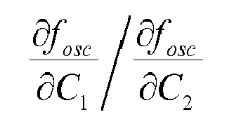

0.5 0.2 0.270 0.276 0.5 1 0.369 0.381 0.125 0.2 0.0183 0.0163 0.125 1 0.0215 0.0196 - In Table 1 shown above, different
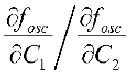
LC tank 100 has a better immunity to device variations. -
FIG. 3 is a diagram illustrating anLC tank 200 according to another embodiment of the present invention. TheLC tank 200 may comprise a portion of the components of theLC tank 100 shown inFIG. 1 and some of the associated connections in theLC tank 100. For example, theLC tank 200 may comprise the inductor L that may be separated into the two series sub-inductors L1 and L2. In addition, theLC tank 200 may further comprise a tunable capacitive array C1 and a capacitive element C2, where the tunable capacitive array C1 (labeled "Cap Array" inFIG. 3 , for brevity) may comprise a plurality of tunable capacitive units which are independently controllable (e.g. the tunable capacitive units can be independently controlled). For example, each tunable capacitive unit of the plurality of tunable capacitive units can be a switchable capacitor unit, and therefore the tunable capacitive array C1 can be a switchable capacitor array. - As shown in
FIG. 3 , the tunable capacitive array C1 of this embodiment can be a capacitor array which is constructed by a plurality of switchable capacitor units C1(1), C1(2), ..., and C1(n) (e.g. the notation "n" may represent a positive integer, such as a positive integer that is greater than one), wherein the capacitance of the switchable capacitor units C1(1), C1(2), ..., and C1(n) can be controlled independently. In addition, the switchable capacitive element C2 shown inFIG. 1 can be replaced by the capacitive element C2 in this embodiment, while the tunable capacitive array C1 of this embodiment can be taken as an example of the switchable capacitive elements C1 shown inFIG. 1 . In some embodiments (e.g. the embodiment shown inFIG. 3 ), if the tunable capacitive array C1 such as the aforementioned switchable capacitor array is designed to have identical switchable capacitor units, the delta frequency (e.g. the frequency difference) per unit capacitance change can be very uniform over the control codes. -
FIG. 4 illustrates a relationship between the differential non-linearity (labeled "DNL" inFIG. 4 , for brevity) and the control codes (labeled "Code" inFIG. 4 , for brevity) according to an embodiment of the present invention. As shown inFIG. 4 , the differential non-linearity over the control codes can be as small as 0.05LSB, i.e. 5% of the equivalent amount corresponding to the least significant bit (LSB). -
FIG. 5 is a diagram illustrating an LC tank according to a second embodiment of the present invention. The differentialmulti-order LC tank 300 comprises two inductors LP and LN and switchable capacitive elements C1 and C2. Specifically, capacitor devices may be placed in each switchable capacitive element C1 and C2. The capacitor devices can be switched on or off via switches depending on a provided data word. Note that the number of devices is not limited in this invention. Moreover, the switchable capacitive elements C1 and C2 may be replaced by analog capacitors in other designs. The switchable capacitive element C2 is coupled between a terminal N1 of the inductor LP and a terminal N3 of the inductor LN. The switchable capacitive element C1 is coupled between a point VxP on the inductor LP and a point VxN on the inductor LN, wherein the points VxP and VxN may be arbitrarily selected according to design specifications. The inductor LP is separated into two series sub-inductors L1 and L2 by the point VxP, and the inductor LN is separated into two series sub-inductors L3 and L4 by the point VxN. Note that an inductance (hereinafter, LP) of the inductor LP equals the sum of the inductances (hereinafter, L1 and L2) of the inductors L1 and L2; and an inductance (hereinafter, LN) of the inductor LN equals the sum of the inductances (hereinafter, L3 and L4) of the inductors L3 and L4. In practice, the point VxP may be any point on the inductor LP other than the terminal N1 and another terminal N2; the point VxN may be any point on the inductor LN other than the terminal N3 and another terminal N4. Preferably, L1 is smaller than L2, and L3 is smaller than L4; however, L1<L2 and L3<L4 is not a limitation of the invention. The terminal N2 is coupled to the terminal N4. - The
LC tank 300 is capable of operating with different system standards by controlling the switchable capacitive element C2, although this may be an optional feature in some applications. Hence, the switchable capacitive element C2 is not essential to the invention. The concept of theLC tank 300 is similar to theLC tank 100 except that theLC tank 300 is for differential architecture. Those skilled in the art should readily understand the operation of theLC tank 300 after reading the descriptions pertaining to theLC tanks - The switchable capacitive element C1 of the
LC tank 300 may be replaced by two switchable capacitive elements C3 and C4 as shown inFIG. 6 according to a third embodiment of the present invention. InFIG. 6 , the switchable capacitive elements C3 and C4 can be adjusted independently. To put it another way, theLC tank 400 may be adjusted asymmetrically for certain usage, for instance, to offset the inherent mismatch of theLC tank 400. Those skilled in the art should readily understand the operation of theLC tank 400 after reading the descriptions regarding theLC tanks - According to some embodiments, implementation of the switchable capacitive element C2 in the architecture shown in
FIG. 6 may vary. For example, the switchable capacitive element C2 of theLC tank 400 may be replaced by two switchable capacitive elements C5 and C6, and the associated connections of the two switchable capacitive elements C5 and C6 may be similar to that of the two switchable capacitive elements C3 and C4 shown inFIG. 6 , respectively, e.g. the switchable capacitive element C5 may be coupled between the terminal N1 and a reference voltage such as the ground voltage and the switchable capacitive element C6 may be coupled between the terminal N3 and a reference voltage such as the ground voltage. This is for illustrative purposes only, and is not meant to be a limitation of the present invention. According to some other embodiments of the present invention, one of the switchable capacitive elements C5 and C6 may be removed from the LC tank of the above embodiments. According to some other embodiments of the present invention, the switchable capacitive element C2 of theLC tank 400 may be replaced by the two switchable capacitive elements C5 and C6, where the two switchable capacitive elements C5 and C6 may be connected in series between the terminals N1 and N3, e.g. the switchable capacitive element C5 may be coupled between the terminal N1 and the switchable capacitive element C6 and the switchable capacitive element C6 may be coupled between the terminal N3 and the switchable capacitive element C5. - According to some embodiments of the present invention, at least one portion (e.g. a portion or all) of the switchable capacitive elements C5 and C6 may be replaced by non-switchable capacitive element(s). For example, in the LC tank of these embodiments, the capacitive element C2 shown in
FIG. 3 can be taken as an example of the non-switchable capacitive element(s) described above. -
FIG. 7 shows a topology of a portion of the LC tank of the present invention. The left half of thecoil 502 may represent the inductor LP shown inFIG. 5 andFIG. 6 , and the right half of thecoil 504 may represent the inductor LN shown inFIG. 5 andFIG. 6 . The inductors form an octagonal geometry as a whole. The ports (the terminals N1 and N3) of the inductors are located in the same corner of the octagonal shape. In other embodiments, the inductors may have other polygonal shapes. In more detail, the point VxP is located at the center point on theleft coil 502, i.e. the inductor LP, and theleft coil 502 is separated into two parts, i.e. the upper inductor L1 and the bottom inductor L2. Note that the upper inductor L1 and the bottom inductor L2 have substantially the same length inFIG. 7 , but this is not a limitation of the invention. Similarly, the point VxN is located at the center point on theright coil 504, i.e. the inductor LN, and theright coil 504 is separated into two parts, i.e. the upper inductor L3 and the bottom inductor L4. Note that the upper inductor L3 and the bottom inductor L4 have substantially the same length inFIG. 7 , but this is not a limitation of the invention. The two ports and the points VxP and VxN are further connected to capacitors, which are not shown inFIG. 7 . -
FIG. 8 is a diagram illustrating an LC tank according to a fourth embodiment of the present invention. The differentialmulti-order LC tank 600 comprises two inductors LP and LN and switchable capacitive elements C2, CC and CM. Specifically, capacitor devices may be placed in each switchable capacitive element C2, CC and CM. The capacitor devices can be switched on or off via switches depending on a provided data word. Note that the number of devices is not limited in this invention. Moreover, the switchable capacitive elements C2, CC and CM may be replaced by analog capacitors in other designs. The switchable capacitive element C2 is coupled between a terminal N1 of the inductor LP and a terminal N3 of the inductor LN. The switchable capacitive element CC is coupled between a point VxP2 on the inductor LP and a point VxN2 on the inductor LN, wherein the points VxP2 and VxN2 may be arbitrarily selected according to design specifications. The switchable capacitive element CM is coupled between a point VxP on the inductor LP and a point VxN on the inductor LN, wherein the points VxP and VxN may be arbitrarily selected according to design specifications. The inductor LP is separated into three series sub-inductors L1, L2 and L3 by the points VxP and VxP2, and the inductor LN is separated into three series sub-inductors L4, L5 and L6 by the points VxN and VxN2. Note that an inductance (hereinafter, LP) of the inductor LP equals the sum of the inductances (hereinafter, L1, L2 and L3) of the inductors L1, L2 and L3; and an inductance (hereinafter, LN) of the inductor LN equals the sum of the inductances (hereinafter, L4, L5 and L6) of the inductors L4, L5 and L6. In practice, the points VxP and VxP2 may be any point on the inductor LP other than the terminal N1 and another terminal N2; the points VxN and VxN2 may be any point on the inductor LN other than the terminal N3 and another terminal N4. Preferably, L1 is smaller than a sum of L2 and L3, and L4 is smaller than a sum of L5 and L6; however, L1<L2+ L3 and L4<L5+L6 is not a limitation of the invention. The terminal N2 is coupled to the terminal N4. - The
LC tank 600 is capable of operating with different system standards by controlling the switchable capacitive element C2, although this may be an optional feature in some applications. Hence, the switchable capacitive element C2 is not essential to the invention. The concept of theLC tank 600 is similar to theLC tank 300 except that theLC tank 600 has one more switchable capacitive element. According to equations (2), (4) and Table 1 illustrated above, the switchable capacitive element CC corresponds to a greater
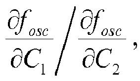

LC tank 600 is required to be calibrated for a specific tuning range, the process will be much more efficient by using the switchable capacitive element CC instead of the switchable capacitive element CM. - In another example, the switchable capacitive element CC can also be used to jointly tune frequency with the switchable capacitive element CM. For instance, the


LC tank 600 may be sent to the switchable capacitive element CM; and the bits greater than the kth bit of the data word may be sent to the switchable capacitive element CC. In this way, both the switchable capacitive element CM and the switchable capacitive element CC can be shrunk to a smaller size. In summary, the disclosedLC tank 600 not only has immunity to variations in the manufacturing process, but also has fast calibration ability. Note that the switchable capacitive element CC may be designed as the switchable capacitive elements C3 and C4 shown inFIG. 6 , as can the switchable capacitive elements CM, in order to adjust theLC tank 400 asymmetrically for certain usage, as mentioned above. -
FIG. 9 shows another topology of a portion of the LC tank of the present invention. InFIG. 9 , a first and a second coupled windings are formed, respectively, by afirst spiral coil 702 and asecond spiral coil 704 supported by a semiconductor substrate, wherein the first andsecond coils first spiral coil 702 represents the inductor LP shown inFIG. 8 , and thesecond spiral coil 704 represents the inductor LN shown inFIG. 8 . The inductors form an octagonal geometry as a whole. The ports (the terminals N1 and N3) of the inductors are located in the same corner of the octagonal shape. In other embodiments, the inductors may have other polygonal shapes. In more detail, the points VxP and VxP2 are located at different points on thefirst spiral coil 702 corresponding to the inductor LP, and thefirst spiral coil 702 is separated into three parts, i.e. the inductors L1, L2 and L3. Note that position of the points VxP and VxP2 are not limited in the invention. Similarly, the points VxN and VxN2 are located at different points on thesecond spiral coil 704 corresponding to the inductor LN, and the inductor LN is separated into three parts, i.e. the inductors L4, L5 and L6. Note that position of the points VxN and VxN2 are not limited in the invention. The two ports and the points VxP, VxP2, VxN and VxN2 are further connected to capacitors, which are not shown inFIG. 9 . - In particular, it is envisaged that the aforementioned inventive concept can be applied by a semiconductor manufacturer to any integrated circuit. It is further envisaged that, for example, a semiconductor manufacturer may employ the inventive concept in the design of a stand-alone device, or application-specific integrated circuit (ASIC) and/or any other sub-system element.
- Although the present invention has been described in connection with some embodiments, it is not intended to be limited to the specific form herein. Rather, the scope of the present invention is limited only by the accompanying claims. Additionally, although a feature may appear to be described in connection with particular embodiments, one skilled in the art would recognize that various features of the described embodiments may be combined in accordance with the invention. In the claims, the term 'comprising' does not exclude the presence of other elements or steps.
- Furthermore, although individually listed, a plurality of means, elements or method steps may be implemented by, for example, a single unit or processor or controller. Additionally, although individual features may be included in different claims, these may possibly be advantageously combined, and the inclusion in different claims does not imply that a combination of features is not feasible and/or advantageous. Also, the inclusion of a feature in one category of claims does not imply a limitation to this category, but rather indicates that the feature is equally applicable to other claim categories, as appropriate. In addition, singular references do not exclude a plurality. Thus, references to 'a', 'an', 'first', 'second', etc. do not preclude a plurality.
- In light of the above, an improved LC tank for a resonator has been described, wherein the aforementioned disadvantages of prior art arrangements have been substantially alleviated.
- All combinations and sub-combinations of above-described features also belong to the invention.
Claims (15)
- An inductor capacitor (LC) tank (100, 200, 400), characterized in that the LC tank comprises:a first inductor (L, LP), having a first terminal (N1) and a second terminal (N2); anda first tunable capacitive array (C1, C1, C3), having a first terminal and a second terminal;wherein the first tunable capacitive array (C1, C1, C3), comprising a plurality of tunable capacitive units (C1(1), C1(2), ..., C1(n)) which are independently controllable, is at a path branching from a first point (VxP) between the first terminal (N1) and the second terminal (N2, N4) of the first inductor (L, LP), the first terminal of the first tunable capacitive array (C1, C1, C3) is coupled to the first point (VxP), and the second terminal of the first tunable capacitive array (C1, C1, C3) and the second terminal (N2) of the first inductor (L, LP) are coupled to a reference voltage.
- The LC tank of claim 1, characterized in that the first tunable capacitive array (C1, C1, C3) is controlled by digital signals.
- The LC tank of claim 1, characterized in that the first tunable capacitive array (C1, C1, C3) is arranged to tune an oscillation frequency of the LC tank.
- The LC tank of claim 1, characterized in that the LC tank further comprises:a first capacitive element (C2, C2) at another path branching from the first terminal (N1) of the first inductor (L, LP), wherein the first capacitive element (C2, C2) has a first terminal coupled to the first terminal (N1) of the first inductor (L, LP) and a second terminal coupled to the reference voltage or another reference voltage.
- The LC tank of claims 1 or 4, characterized in that a portion (L1) of the first inductor (L, LP) from the second terminal (N2) of the first inductor (L, LP) to the first point (VxP) forms a first sub-inductor (L1), another portion (L2) of the first inductor (L, LP) from the first point (VxP) to the first terminal (N1) of the first inductor (L, LP) forms a second sub-inductor (L2), and an inductance of the first sub-inductor (L1) is less than an inductance of the second sub-inductor (L2).
- The LC tank of claims 1 or 4, characterized in that the first inductor (L, LP) is a spiral coil, and a distance from the second terminal (N2) of the first inductor (L, LP) to the first point (VxP) is less than a distance from the first point (VxP) to the first terminal (N1) of the first inductor (L, LP), wherein the distances are measured along sub-coils of the spiral coil.
- The LC tank of claim 1, characterized in that the LC tank further comprises:a second inductor (LN) having a first terminal (N3) and a second terminal (N4), wherein the second terminal (N4) of the second inductor (LN) is coupled to the second terminal(N2) of the first inductor (LP).
- The LC tank of claim 7, characterized in that the LC tank further comprises:a second tunable capacitive array (C4) at another path branching from a second point (VxN) between the first terminal (N3) and the second terminal (N4) of the second inductor (LN), wherein the second tunable capacitive array (C4) has a first terminal and a second terminal, the first terminal of the second tunable capacitive array (C4) is coupled to the second point (VxN), and the second terminal of the second tunable capacitive array (C4) is coupled to the reference voltage or another reference voltage.
- The LC tank of claim 8, characterized in that the second tunable capacitive array (C4) is arranged to tune an oscillation frequency of the LC tank.
- The LC tank of claim 8, characterized in that a portion (L3) of the second inductor (LN) from the second terminal (N4) of the second inductor (LN) to the second point (VxN) forms a first sub-inductor (L3), another portion (L4) of the second inductor (LN) from the second point (VxN) to the first terminal (N3) of the second inductor (LN) forms a second sub-inductor (L4), and an inductance of the first sub-inductor (L3) is less than an inductance of the second sub-inductor (L4).
- The LC tank of claim 8, characterized in that the second inductor (LN) is a spiral coil, and a distance from the second terminal (N4) of the second inductor (LN) to the second point (VxN) is less than a distance from the second point (VxN) to the first terminal (N3) of the second inductor (LN), wherein the distances are measured along sub-coils of the spiral coil.
- An inductor capacitor (LC) tank (300, 600), characterized in that the LC tank comprises:a first inductor (LP), having a first terminal (N1) and a second terminal (N2);a second inductor (LN), having a first terminal (N3) and a second terminal (N4), wherein the second terminal (N4) of the second inductor (LN) and the second terminal (N2) of the first inductor (LP) are coupled to each other; anda first tunable capacitive array (C1, CM), having a first terminal and a second terminal;wherein the first tunable capacitive array (C1, CM) is at a path branching from a first point (VxP) between the first terminal (N1) and the second terminal (N2) of the first inductor (LP) to a second point (VxN) between the first terminal (N3) and the second terminal (N4) of the second inductor (LN), the first terminal of the first tunable capacitive array (C1, CM) is coupled to the first point (VxP), and the second terminal of the first tunable capacitive array (C1, CM) is coupled to the second point (VxN).
- The LC tank of claim 12, characterized in that a portion (L1) of the first inductor (LP) from the second terminal (N2) of the first inductor (LP) to the first point (VxP) forms a first sub-inductor (L1), another portion (L2) of the first inductor (LP) from the first point (VxP) to the first terminal (N1) of the first inductor (LP) forms a second sub-inductor (L2), and an inductance of the first sub-inductor (L1) is less than an inductance of the second sub-inductor (L2); and a portion (L3) of the second inductor (LN) from the second terminal (N4) of the second inductor (LN) to the second point (VxN) forms a third sub-inductor (L3), another portion (L4) of the second inductor (LN) from the second point (VxN) to the first terminal (N3) of the second inductor (LN) forms a fourth sub-inductor (L4), and an inductance of the third sub-inductor (L3) is less than an inductance of the fourth sub-inductor (L4).
- The LC tank of claim 12, characterized in that the first inductor (LP) is a spiral coil, and a first distance from the second terminal (N2) of the first inductor (LP) to the first point (VxP) is less than a second distance from the first point (VxP) to the first terminal (N1) of the first inductor (LP), wherein the first distance and the second distance are measured along sub-coils of the spiral coil; and the second inductor (LN) is another spiral coil, and a third distance from the second terminal (N4) of the second inductor (LN) to the second point (VxN) is less than a fourth distance from the second point (VxN) to the first terminal (N3) of the second inductor (LN), wherein the third distance and the fourth distance are measured along sub-coils of the spiral coil.
- The LC tank of claim 12, characterized in that the LC tank further comprises:a second tunable capacitive array (CC), having a first terminal and a second terminal, wherein the second tunable capacitive array (CC) is at another path branching from a third point (VxP2) between the first point (VxP) and the first terminal (N1) of the first inductor (LP) to a fourth point (VxN2) between the second point (VxN)and the first terminal (N3) of the second inductor (LN), the first terminal of the second tunable capacitive array (CC) is coupled to the third point (VxP2), and the second terminal of the second tunable capacitive array (CC) is coupled to the fourth point (VxN2).
Applications Claiming Priority (2)
| Application Number | Priority Date | Filing Date | Title |
|---|---|---|---|
| US201562161850P | 2015-05-14 | 2015-05-14 | |
| US15/050,436 US9948265B2 (en) | 2015-05-14 | 2016-02-22 | Inductor capacitor tank for resonator |
Publications (2)
| Publication Number | Publication Date |
|---|---|
| EP3093989A1 true EP3093989A1 (en) | 2016-11-16 |
| EP3093989B1 EP3093989B1 (en) | 2018-05-16 |
Family
ID=55453094
Family Applications (1)
| Application Number | Title | Priority Date | Filing Date |
|---|---|---|---|
| EP16158392.7A Active EP3093989B1 (en) | 2015-05-14 | 2016-03-03 | Inductor capacitor tank for resonator |
Country Status (3)
| Country | Link |
|---|---|
| US (1) | US9948265B2 (en) |
| EP (1) | EP3093989B1 (en) |
| CN (1) | CN106160667B (en) |
Families Citing this family (9)
| Publication number | Priority date | Publication date | Assignee | Title |
|---|---|---|---|---|
| US20190189342A1 (en) * | 2017-12-20 | 2019-06-20 | National Chung Shan Institute Of Science And Technology | Variable inductor and integrated circuit using the variable inductor |
| US12488931B2 (en) * | 2019-09-11 | 2025-12-02 | Realtek Semiconductor Corporation | Inductor device |
| US12062480B2 (en) * | 2019-09-11 | 2024-08-13 | Realtek Semiconductor Corporation | Inductor device |
| US11869700B2 (en) * | 2019-09-11 | 2024-01-09 | Realtek Semiconductor Corporation | Inductor device |
| US12548707B2 (en) * | 2019-09-11 | 2026-02-10 | Realtek Semiconductor Corporation | Inductor device |
| US11901399B2 (en) | 2019-09-11 | 2024-02-13 | Realtek Semiconductor Corporation | Enhanced sensing coil for semiconductor device |
| WO2022015758A1 (en) | 2020-07-14 | 2022-01-20 | Cornell University | A tunable resonator |
| US11658647B2 (en) * | 2020-08-19 | 2023-05-23 | Intrinsix Corp. | Adjustable delay line devices and methods thereof |
| CN115966369B (en) * | 2021-10-13 | 2026-01-27 | 瑞昱半导体股份有限公司 | Inductance device |
Citations (5)
| Publication number | Priority date | Publication date | Assignee | Title |
|---|---|---|---|---|
| EP1858155A1 (en) * | 2006-05-17 | 2007-11-21 | ATMEL Duisburg GmbH | Integrated resonator circuit |
| US20100052817A1 (en) * | 2008-09-03 | 2010-03-04 | Siqi Fan | Integrated Circuit Inductor with Transverse Interfaces |
| EP2355340A1 (en) * | 2010-02-04 | 2011-08-10 | Hittite Microwave Corporation | Wideband analog lowpass filter |
| US20140285299A1 (en) * | 2013-03-15 | 2014-09-25 | Wispry, Inc. | Tuning systems, devices and methods |
| US20150097637A1 (en) * | 2013-10-09 | 2015-04-09 | Analog Devices, Inc. | Programmable filter |
Family Cites Families (7)
| Publication number | Priority date | Publication date | Assignee | Title |
|---|---|---|---|---|
| KR20080072642A (en) * | 2005-10-31 | 2008-08-06 | 엠케이에스 인스트루먼츠, 인코포레이티드 | High frequency power delivery system |
| US8565709B2 (en) * | 2010-12-30 | 2013-10-22 | Apple Inc. | Digital signal filter |
| US9313053B2 (en) * | 2012-05-15 | 2016-04-12 | Broadcom Corporation | Filter circuitry |
| US9118335B2 (en) | 2012-09-16 | 2015-08-25 | Technische Universiteit Delft | High resolution millimeter wave digitally controlled oscillator with reconfigurable distributed metal capacitor passive resonators |
| US9270248B2 (en) * | 2012-10-12 | 2016-02-23 | Infineon Technologies Ag | Impedance matching network with improved quality factor and method for matching an impedance |
| US9276547B2 (en) * | 2013-06-28 | 2016-03-01 | Peregrine Semiconductor Corporation | Systems and methods of stacking LC tanks for wide tuning range and high voltage swing |
| US9667217B2 (en) * | 2015-04-17 | 2017-05-30 | Peregrine Semiconductor Corporation | High performance integrated tunable impedance matching network with coupled merged inductors |
-
2016
- 2016-02-22 US US15/050,436 patent/US9948265B2/en active Active
- 2016-03-03 EP EP16158392.7A patent/EP3093989B1/en active Active
- 2016-05-10 CN CN201610303974.6A patent/CN106160667B/en active Active
Patent Citations (5)
| Publication number | Priority date | Publication date | Assignee | Title |
|---|---|---|---|---|
| EP1858155A1 (en) * | 2006-05-17 | 2007-11-21 | ATMEL Duisburg GmbH | Integrated resonator circuit |
| US20100052817A1 (en) * | 2008-09-03 | 2010-03-04 | Siqi Fan | Integrated Circuit Inductor with Transverse Interfaces |
| EP2355340A1 (en) * | 2010-02-04 | 2011-08-10 | Hittite Microwave Corporation | Wideband analog lowpass filter |
| US20140285299A1 (en) * | 2013-03-15 | 2014-09-25 | Wispry, Inc. | Tuning systems, devices and methods |
| US20150097637A1 (en) * | 2013-10-09 | 2015-04-09 | Analog Devices, Inc. | Programmable filter |
Also Published As
| Publication number | Publication date |
|---|---|
| CN106160667A (en) | 2016-11-23 |
| CN106160667B (en) | 2019-04-02 |
| US20160336914A1 (en) | 2016-11-17 |
| EP3093989B1 (en) | 2018-05-16 |
| US9948265B2 (en) | 2018-04-17 |
Similar Documents
| Publication | Publication Date | Title |
|---|---|---|
| EP3093989B1 (en) | Inductor capacitor tank for resonator | |
| CN105190880B (en) | Circuit and method for multi-mode filter | |
| JP3877597B2 (en) | Multi-terminal MOS varactor | |
| US5952893A (en) | Integrated circuit inductors for use with electronic oscillators | |
| US10862424B2 (en) | Parallel-based switching inductor device | |
| US20050052272A1 (en) | Inductive component | |
| US8072280B2 (en) | Voltage-controlled oscillator | |
| CN102938644B (en) | Numerically-controlled oscillator | |
| US9589916B2 (en) | Inductively coupled transformer with tunable impedance match network | |
| US20160191009A1 (en) | Tunable resonator | |
| US7915968B2 (en) | Digitally controlled oscillator (DCO) | |
| US9071193B1 (en) | System and method for augmenting frequency tuning resolution in L-C oscillation circuit | |
| US9425736B2 (en) | Variable capacitor structure | |
| US20190229677A1 (en) | Semiconductor Device and Method | |
| US20040061563A1 (en) | Oscillator | |
| CN104993794A (en) | High-precision digital control LC oscillator employing inductive tap | |
| EP2434639A1 (en) | LC oscillator with switchable capacitive array | |
| CN110350870B (en) | Class-F2 voltage-controlled oscillator | |
| US7782160B2 (en) | Central frequency adjustment device and adjustable inductor layout using trimmable wire | |
| KR100441985B1 (en) | High frequency integrated circuit and integrated high frequency semiconductor device | |
| US5959503A (en) | Voltage controlled oscillator tuning by metal lid aperture selection | |
| US6060759A (en) | Method and apparatus for creating improved inductors for use with electronic oscillators | |
| US11196382B1 (en) | Oscillator with inductor and programmable capacitor bank | |
| JP2021090184A (en) | SELF-CALIBRATED Soc | |
| EP4525301A2 (en) | Inductive-capacitive voltage-controlled oscillator with increased common-mode impedance |
Legal Events
| Date | Code | Title | Description |
|---|---|---|---|
| PUAI | Public reference made under article 153(3) epc to a published international application that has entered the european phase |
Free format text: ORIGINAL CODE: 0009012 |
|
| AK | Designated contracting states |
Kind code of ref document: A1 Designated state(s): AL AT BE BG CH CY CZ DE DK EE ES FI FR GB GR HR HU IE IS IT LI LT LU LV MC MK MT NL NO PL PT RO RS SE SI SK SM TR |
|
| AX | Request for extension of the european patent |
Extension state: BA ME |
|
| 17P | Request for examination filed |
Effective date: 20170426 |
|
| RBV | Designated contracting states (corrected) |
Designated state(s): AL AT BE BG CH CY CZ DE DK EE ES FI FR GB GR HR HU IE IS IT LI LT LU LV MC MK MT NL NO PL PT RO RS SE SI SK SM TR |
|
| STAA | Information on the status of an ep patent application or granted ep patent |
Free format text: STATUS: REQUEST FOR EXAMINATION WAS MADE |
|
| STAA | Information on the status of an ep patent application or granted ep patent |
Free format text: STATUS: EXAMINATION IS IN PROGRESS |
|
| 17Q | First examination report despatched |
Effective date: 20170629 |
|
| GRAP | Despatch of communication of intention to grant a patent |
Free format text: ORIGINAL CODE: EPIDOSNIGR1 |
|
| STAA | Information on the status of an ep patent application or granted ep patent |
Free format text: STATUS: GRANT OF PATENT IS INTENDED |
|
| INTG | Intention to grant announced |
Effective date: 20180124 |
|
| GRAS | Grant fee paid |
Free format text: ORIGINAL CODE: EPIDOSNIGR3 |
|
| GRAA | (expected) grant |
Free format text: ORIGINAL CODE: 0009210 |
|
| STAA | Information on the status of an ep patent application or granted ep patent |
Free format text: STATUS: THE PATENT HAS BEEN GRANTED |
|
| AK | Designated contracting states |
Kind code of ref document: B1 Designated state(s): AL AT BE BG CH CY CZ DE DK EE ES FI FR GB GR HR HU IE IS IT LI LT LU LV MC MK MT NL NO PL PT RO RS SE SI SK SM TR |
|
| REG | Reference to a national code |
Ref country code: GB Ref legal event code: FG4D |
|
| REG | Reference to a national code |
Ref country code: CH Ref legal event code: EP |
|
| REG | Reference to a national code |
Ref country code: IE Ref legal event code: FG4D |
|
| REG | Reference to a national code |
Ref country code: DE Ref legal event code: R096 Ref document number: 602016003034 Country of ref document: DE |
|
| REG | Reference to a national code |
Ref country code: AT Ref legal event code: REF Ref document number: 1000456 Country of ref document: AT Kind code of ref document: T Effective date: 20180615 |
|
| REG | Reference to a national code |
Ref country code: NL Ref legal event code: MP Effective date: 20180516 |
|
| REG | Reference to a national code |
Ref country code: LT Ref legal event code: MG4D |
|
| PG25 | Lapsed in a contracting state [announced via postgrant information from national office to epo] |
Ref country code: NO Free format text: LAPSE BECAUSE OF FAILURE TO SUBMIT A TRANSLATION OF THE DESCRIPTION OR TO PAY THE FEE WITHIN THE PRESCRIBED TIME-LIMIT Effective date: 20180816 Ref country code: ES Free format text: LAPSE BECAUSE OF FAILURE TO SUBMIT A TRANSLATION OF THE DESCRIPTION OR TO PAY THE FEE WITHIN THE PRESCRIBED TIME-LIMIT Effective date: 20180516 Ref country code: LT Free format text: LAPSE BECAUSE OF FAILURE TO SUBMIT A TRANSLATION OF THE DESCRIPTION OR TO PAY THE FEE WITHIN THE PRESCRIBED TIME-LIMIT Effective date: 20180516 Ref country code: SE Free format text: LAPSE BECAUSE OF FAILURE TO SUBMIT A TRANSLATION OF THE DESCRIPTION OR TO PAY THE FEE WITHIN THE PRESCRIBED TIME-LIMIT Effective date: 20180516 Ref country code: FI Free format text: LAPSE BECAUSE OF FAILURE TO SUBMIT A TRANSLATION OF THE DESCRIPTION OR TO PAY THE FEE WITHIN THE PRESCRIBED TIME-LIMIT Effective date: 20180516 Ref country code: BG Free format text: LAPSE BECAUSE OF FAILURE TO SUBMIT A TRANSLATION OF THE DESCRIPTION OR TO PAY THE FEE WITHIN THE PRESCRIBED TIME-LIMIT Effective date: 20180816 |
|
| PG25 | Lapsed in a contracting state [announced via postgrant information from national office to epo] |
Ref country code: RS Free format text: LAPSE BECAUSE OF FAILURE TO SUBMIT A TRANSLATION OF THE DESCRIPTION OR TO PAY THE FEE WITHIN THE PRESCRIBED TIME-LIMIT Effective date: 20180516 Ref country code: NL Free format text: LAPSE BECAUSE OF FAILURE TO SUBMIT A TRANSLATION OF THE DESCRIPTION OR TO PAY THE FEE WITHIN THE PRESCRIBED TIME-LIMIT Effective date: 20180516 Ref country code: LV Free format text: LAPSE BECAUSE OF FAILURE TO SUBMIT A TRANSLATION OF THE DESCRIPTION OR TO PAY THE FEE WITHIN THE PRESCRIBED TIME-LIMIT Effective date: 20180516 Ref country code: GR Free format text: LAPSE BECAUSE OF FAILURE TO SUBMIT A TRANSLATION OF THE DESCRIPTION OR TO PAY THE FEE WITHIN THE PRESCRIBED TIME-LIMIT Effective date: 20180817 Ref country code: HR Free format text: LAPSE BECAUSE OF FAILURE TO SUBMIT A TRANSLATION OF THE DESCRIPTION OR TO PAY THE FEE WITHIN THE PRESCRIBED TIME-LIMIT Effective date: 20180516 |
|
| REG | Reference to a national code |
Ref country code: AT Ref legal event code: MK05 Ref document number: 1000456 Country of ref document: AT Kind code of ref document: T Effective date: 20180516 |
|
| PG25 | Lapsed in a contracting state [announced via postgrant information from national office to epo] |
Ref country code: RO Free format text: LAPSE BECAUSE OF FAILURE TO SUBMIT A TRANSLATION OF THE DESCRIPTION OR TO PAY THE FEE WITHIN THE PRESCRIBED TIME-LIMIT Effective date: 20180516 Ref country code: SK Free format text: LAPSE BECAUSE OF FAILURE TO SUBMIT A TRANSLATION OF THE DESCRIPTION OR TO PAY THE FEE WITHIN THE PRESCRIBED TIME-LIMIT Effective date: 20180516 Ref country code: EE Free format text: LAPSE BECAUSE OF FAILURE TO SUBMIT A TRANSLATION OF THE DESCRIPTION OR TO PAY THE FEE WITHIN THE PRESCRIBED TIME-LIMIT Effective date: 20180516 Ref country code: DK Free format text: LAPSE BECAUSE OF FAILURE TO SUBMIT A TRANSLATION OF THE DESCRIPTION OR TO PAY THE FEE WITHIN THE PRESCRIBED TIME-LIMIT Effective date: 20180516 Ref country code: AT Free format text: LAPSE BECAUSE OF FAILURE TO SUBMIT A TRANSLATION OF THE DESCRIPTION OR TO PAY THE FEE WITHIN THE PRESCRIBED TIME-LIMIT Effective date: 20180516 Ref country code: PL Free format text: LAPSE BECAUSE OF FAILURE TO SUBMIT A TRANSLATION OF THE DESCRIPTION OR TO PAY THE FEE WITHIN THE PRESCRIBED TIME-LIMIT Effective date: 20180516 Ref country code: CZ Free format text: LAPSE BECAUSE OF FAILURE TO SUBMIT A TRANSLATION OF THE DESCRIPTION OR TO PAY THE FEE WITHIN THE PRESCRIBED TIME-LIMIT Effective date: 20180516 |
|
| REG | Reference to a national code |
Ref country code: DE Ref legal event code: R097 Ref document number: 602016003034 Country of ref document: DE |
|
| PG25 | Lapsed in a contracting state [announced via postgrant information from national office to epo] |
Ref country code: IT Free format text: LAPSE BECAUSE OF FAILURE TO SUBMIT A TRANSLATION OF THE DESCRIPTION OR TO PAY THE FEE WITHIN THE PRESCRIBED TIME-LIMIT Effective date: 20180516 Ref country code: SM Free format text: LAPSE BECAUSE OF FAILURE TO SUBMIT A TRANSLATION OF THE DESCRIPTION OR TO PAY THE FEE WITHIN THE PRESCRIBED TIME-LIMIT Effective date: 20180516 |
|
| PLBE | No opposition filed within time limit |
Free format text: ORIGINAL CODE: 0009261 |
|
| STAA | Information on the status of an ep patent application or granted ep patent |
Free format text: STATUS: NO OPPOSITION FILED WITHIN TIME LIMIT |
|
| 26N | No opposition filed |
Effective date: 20190219 |
|
| PG25 | Lapsed in a contracting state [announced via postgrant information from national office to epo] |
Ref country code: SI Free format text: LAPSE BECAUSE OF FAILURE TO SUBMIT A TRANSLATION OF THE DESCRIPTION OR TO PAY THE FEE WITHIN THE PRESCRIBED TIME-LIMIT Effective date: 20180516 |
|
| PG25 | Lapsed in a contracting state [announced via postgrant information from national office to epo] |
Ref country code: MC Free format text: LAPSE BECAUSE OF FAILURE TO SUBMIT A TRANSLATION OF THE DESCRIPTION OR TO PAY THE FEE WITHIN THE PRESCRIBED TIME-LIMIT Effective date: 20180516 |
|
| REG | Reference to a national code |
Ref country code: CH Ref legal event code: PL |
|
| PG25 | Lapsed in a contracting state [announced via postgrant information from national office to epo] |
Ref country code: AL Free format text: LAPSE BECAUSE OF FAILURE TO SUBMIT A TRANSLATION OF THE DESCRIPTION OR TO PAY THE FEE WITHIN THE PRESCRIBED TIME-LIMIT Effective date: 20180516 Ref country code: LU Free format text: LAPSE BECAUSE OF NON-PAYMENT OF DUE FEES Effective date: 20190303 |
|
| REG | Reference to a national code |
Ref country code: BE Ref legal event code: MM Effective date: 20190331 |
|
| PG25 | Lapsed in a contracting state [announced via postgrant information from national office to epo] |
Ref country code: IE Free format text: LAPSE BECAUSE OF NON-PAYMENT OF DUE FEES Effective date: 20190303 Ref country code: LI Free format text: LAPSE BECAUSE OF NON-PAYMENT OF DUE FEES Effective date: 20190331 Ref country code: CH Free format text: LAPSE BECAUSE OF NON-PAYMENT OF DUE FEES Effective date: 20190331 |
|
| PG25 | Lapsed in a contracting state [announced via postgrant information from national office to epo] |
Ref country code: BE Free format text: LAPSE BECAUSE OF NON-PAYMENT OF DUE FEES Effective date: 20190331 |
|
| PG25 | Lapsed in a contracting state [announced via postgrant information from national office to epo] |
Ref country code: TR Free format text: LAPSE BECAUSE OF FAILURE TO SUBMIT A TRANSLATION OF THE DESCRIPTION OR TO PAY THE FEE WITHIN THE PRESCRIBED TIME-LIMIT Effective date: 20180516 |
|
| PG25 | Lapsed in a contracting state [announced via postgrant information from national office to epo] |
Ref country code: PT Free format text: LAPSE BECAUSE OF FAILURE TO SUBMIT A TRANSLATION OF THE DESCRIPTION OR TO PAY THE FEE WITHIN THE PRESCRIBED TIME-LIMIT Effective date: 20180917 Ref country code: MT Free format text: LAPSE BECAUSE OF NON-PAYMENT OF DUE FEES Effective date: 20190303 |
|
| PG25 | Lapsed in a contracting state [announced via postgrant information from national office to epo] |
Ref country code: CY Free format text: LAPSE BECAUSE OF FAILURE TO SUBMIT A TRANSLATION OF THE DESCRIPTION OR TO PAY THE FEE WITHIN THE PRESCRIBED TIME-LIMIT Effective date: 20180516 |
|
| PG25 | Lapsed in a contracting state [announced via postgrant information from national office to epo] |
Ref country code: IS Free format text: LAPSE BECAUSE OF FAILURE TO SUBMIT A TRANSLATION OF THE DESCRIPTION OR TO PAY THE FEE WITHIN THE PRESCRIBED TIME-LIMIT Effective date: 20180916 |
|
| PG25 | Lapsed in a contracting state [announced via postgrant information from national office to epo] |
Ref country code: HU Free format text: LAPSE BECAUSE OF FAILURE TO SUBMIT A TRANSLATION OF THE DESCRIPTION OR TO PAY THE FEE WITHIN THE PRESCRIBED TIME-LIMIT; INVALID AB INITIO Effective date: 20160303 |
|
| PG25 | Lapsed in a contracting state [announced via postgrant information from national office to epo] |
Ref country code: MK Free format text: LAPSE BECAUSE OF FAILURE TO SUBMIT A TRANSLATION OF THE DESCRIPTION OR TO PAY THE FEE WITHIN THE PRESCRIBED TIME-LIMIT Effective date: 20180516 |
|
| P01 | Opt-out of the competence of the unified patent court (upc) registered |
Effective date: 20230607 |
|
| PGFP | Annual fee paid to national office [announced via postgrant information from national office to epo] |
Ref country code: FR Payment date: 20251231 Year of fee payment: 11 |
|
| PGFP | Annual fee paid to national office [announced via postgrant information from national office to epo] |
Ref country code: GB Payment date: 20260106 Year of fee payment: 11 |
|
| PGFP | Annual fee paid to national office [announced via postgrant information from national office to epo] |
Ref country code: DE Payment date: 20260102 Year of fee payment: 11 |