EP3093948A2 - Voltage regulation in wireless power receiver - Google Patents
Voltage regulation in wireless power receiver Download PDFInfo
- Publication number
- EP3093948A2 EP3093948A2 EP16164774.8A EP16164774A EP3093948A2 EP 3093948 A2 EP3093948 A2 EP 3093948A2 EP 16164774 A EP16164774 A EP 16164774A EP 3093948 A2 EP3093948 A2 EP 3093948A2
- Authority
- EP
- European Patent Office
- Prior art keywords
- voltage
- output
- range
- rectifier
- capacitor
- Prior art date
- Legal status (The legal status is an assumption and is not a legal conclusion. Google has not performed a legal analysis and makes no representation as to the accuracy of the status listed.)
- Pending
Links
Images



Classifications
-
- B—PERFORMING OPERATIONS; TRANSPORTING
- B60—VEHICLES IN GENERAL
- B60L—PROPULSION OF ELECTRICALLY-PROPELLED VEHICLES; SUPPLYING ELECTRIC POWER FOR AUXILIARY EQUIPMENT OF ELECTRICALLY-PROPELLED VEHICLES; ELECTRODYNAMIC BRAKE SYSTEMS FOR VEHICLES IN GENERAL; MAGNETIC SUSPENSION OR LEVITATION FOR VEHICLES; MONITORING OPERATING VARIABLES OF ELECTRICALLY-PROPELLED VEHICLES; ELECTRIC SAFETY DEVICES FOR ELECTRICALLY-PROPELLED VEHICLES
- B60L3/00—Electric devices on electrically-propelled vehicles for safety purposes; Monitoring operating variables, e.g. speed, deceleration or energy consumption
-
- H—ELECTRICITY
- H02—GENERATION; CONVERSION OR DISTRIBUTION OF ELECTRIC POWER
- H02J—ELECTRIC POWER NETWORKS; CIRCUIT ARRANGEMENTS OR SYSTEMS FOR SUPPLYING OR DISTRIBUTING ELECTRIC POWER; SYSTEMS FOR STORING ELECTRIC ENERGY
- H02J50/00—Circuit arrangements or systems for wireless supply or distribution of electric power
- H02J50/10—Circuit arrangements or systems for wireless supply or distribution of electric power using inductive coupling
- H02J50/12—Circuit arrangements or systems for wireless supply or distribution of electric power using inductive coupling of the resonant type
-
- B—PERFORMING OPERATIONS; TRANSPORTING
- B60—VEHICLES IN GENERAL
- B60L—PROPULSION OF ELECTRICALLY-PROPELLED VEHICLES; SUPPLYING ELECTRIC POWER FOR AUXILIARY EQUIPMENT OF ELECTRICALLY-PROPELLED VEHICLES; ELECTRODYNAMIC BRAKE SYSTEMS FOR VEHICLES IN GENERAL; MAGNETIC SUSPENSION OR LEVITATION FOR VEHICLES; MONITORING OPERATING VARIABLES OF ELECTRICALLY-PROPELLED VEHICLES; ELECTRIC SAFETY DEVICES FOR ELECTRICALLY-PROPELLED VEHICLES
- B60L1/00—Supplying electric power to auxiliary equipment of vehicles
-
- H—ELECTRICITY
- H01—ELECTRIC ELEMENTS
- H01F—MAGNETS; INDUCTANCES; TRANSFORMERS; SELECTION OF MATERIALS FOR THEIR MAGNETIC PROPERTIES
- H01F27/00—Details of transformers or inductances, in general
- H01F27/08—Cooling; Ventilating
- H01F27/10—Liquid cooling
- H01F27/16—Water cooling
-
- H—ELECTRICITY
- H02—GENERATION; CONVERSION OR DISTRIBUTION OF ELECTRIC POWER
- H02J—ELECTRIC POWER NETWORKS; CIRCUIT ARRANGEMENTS OR SYSTEMS FOR SUPPLYING OR DISTRIBUTING ELECTRIC POWER; SYSTEMS FOR STORING ELECTRIC ENERGY
- H02J1/00—Circuit arrangements for DC mains or DC distribution networks
- H02J1/10—Parallel operation of DC sources
-
- H—ELECTRICITY
- H02—GENERATION; CONVERSION OR DISTRIBUTION OF ELECTRIC POWER
- H02J—ELECTRIC POWER NETWORKS; CIRCUIT ARRANGEMENTS OR SYSTEMS FOR SUPPLYING OR DISTRIBUTING ELECTRIC POWER; SYSTEMS FOR STORING ELECTRIC ENERGY
- H02J7/00—Circuit arrangements for charging or discharging batteries or for supplying loads from batteries
- H02J7/14—Circuit arrangements for charging or discharging batteries or for supplying loads from batteries for charging batteries from dynamo-electric generators driven at varying speed, e.g. on vehicle
- H02J7/16—Regulation of the charging current or voltage by variation of field
-
- H—ELECTRICITY
- H04—ELECTRIC COMMUNICATION TECHNIQUE
- H04B—TRANSMISSION
- H04B15/00—Suppression or limitation of noise or interference
-
- H—ELECTRICITY
- H04—ELECTRIC COMMUNICATION TECHNIQUE
- H04B—TRANSMISSION
- H04B3/00—Line transmission systems
Definitions
- This disclosure relates generally to techniques for wireless charging. Specifically, this disclosure relates to regulation of voltage in wireless power systems.
- a basic wireless charging system may include a wireless power transmitter unit (PTU) and a wireless power receiving unit (PRU).
- PTU wireless power transmitter unit
- PRU wireless power receiving unit
- a PTU may include a transmit (Tx) coil
- a PRU may include receive (Rx) coil.
- Magnetic resonance wireless charging may employ a magnetic coupling between the Tx coil and the Rx coil.
- wireless power received may vary causing issues with efficiency in wireless charging systems.
- variations of voltage may violate wireless charging standard specifications.
- the present disclosure relates generally to techniques for wireless charging.
- the techniques described herein include a wireless power rectifier and voltage compensation logic to reduce voltage variation of output voltage from the rectifier.
- voltage variations may generate inefficiencies in wireless charging. For example, spatial freedom of placement of a device under charge having a receiver (Rx) coil may result in a potentially large rectified receiver voltage (Vrect) variation. Variations in Vrect may constrain designs by requiring stringent field uniformity in some cases.
- Voltage compensation logic includes one or more electric circuit components, modules, or integrated components configured to reduce variation in voltage.
- voltage compensation logic may be configured to reduce variation of Vrect at a wireless charging component such as a wireless charging receiving coil.
- voltage compensation logic may include one or more of capacitors in a feedback loop configured to reduce variations in Vrect, amplifiers, resistors, and the like.
- I_compensate compensated current source
- the techniques discussed herein may be implemented using a wireless charging standard protocol, such as the specification provided by Alliance For Wireless Power (A4WP) version 1.2.1, May 07, 2014.
- a wireless power Rx coil may be a component in a power receiving unit (PRU), while a wireless power transmission (Tx) coil may be a component in a power transmitting unit (PTU), as discussed in more detail below.
- a wireless power Rx coil may be a component in a power receiving unit (PRU), while a wireless power transmission (Tx) coil may be a component in a power transmitting unit (PTU), as discussed in more detail below.
- a wireless power Rx coil may be a component in a power receiving unit (PRU)
- Tx wireless power transmission
- PTU power transmitting unit
- the techniques described herein may be implemented using any other wireless charging standard protocol where applicable.
- Fig. 1 is block diagram of a PTU to provide power to a PRU, wherein a magnetic component protrudes from the PTU.
- a PTU 102 may couple to a PRU 104 via magnetic inductive coupling between resonators 106, and108, as indicated by the arrow 110.
- the resonator 106 may be referred to herein as a Tx coil 106 of the PTU 102.
- the resonator 108 may be referred to herein as an Rx coil 108 of the PRU 104.
- the PRU 104 may include logic 112.
- the logic 112 may be referred to herein as voltage compensation logic 112.
- the voltage compensation logic 112 may be configured as an integrated component of a rectifier 114, as a separate component of the rectifier 114, or any combination thereof. In any case, the voltage compensation logic 112 may be configured to reduce variations in Vrect. In other words, the voltage compensation logic 112 may be configured to reduce variations in rectified voltage output by the rectifier 114.
- the voltage compensation logic 112 may be composed of one or more components, such as electronic circuit components, as discussed in more detail below in regard to Fig. 2 and Fig. 5 . For example, the voltage compensation logic 112 may be implemented as a current source to introduce limits on Vrect variation.
- the voltage compensation logic 112 may be implemented using a voltage controlled capacitor in parallel with the Rx coil 108. Additional details are discussed in more detail below in regard to Fig. 2 and Fig. 5 , as well as throughout the present description, Figures, and claims.
- the PRU 104 may include a controller 116 configured to detect current received at the Rx coil 108 resulting from an inductive coupling between the Tx coil 106 and the Rx coil 108.
- the controller 114 may be configured to initiate load modulations to communicate a wireless data broadcast.
- the wireless broadcast may be carried out by a wireless data transmission component such as a Bluetooth Low Energy (BLE) module 118.
- BLE Bluetooth Low Energy
- the wireless data transmission component may be integrated as operations of the controller 116, a load modulation circuit 120, a direct current to direct current (DC2DC) converter 122, or any combination thereof, wherein the data transmission may be indicated by patterns in the load modulation.
- DC2DC direct current to direct current
- the DC2DC converter 122 provides a DC output to a battery 124, or another current/power consuming component.
- the DC2DC converter 122 may convert DC received as a result of the inductive coupling of the Tx coil 106, the Rx coil 108, and the rectifier 114.
- the PTU 102 may include a BLE module 126 configured to communicate with the BLE module 118.
- the PTU 102 may also include a current sensor 128, a controller 130, a power amplifier 132, a DC2DC converter 134, an oscillator 136, and a matching network 138.
- the current sensor 128 may be an ampere meter, a volt meter, or any other sensor configured to sense load variations occurring due to inductive coupling between the PTU 102 and another object, such as the PRU 104.
- the current sensor 128 may provide an indication of load change to the controller 130 of the PTU 102.
- the controller 130 may power on the power amplifier 132 configured to receive direct current (DC) from the DC2DC converter 134, and to amplify and oscillate the current.
- An oscillator 136 may oscillate the power provided at a given frequency and a matching network 138 may be used to match the amplified oscillation provided to the resonator 106 of the PTU 102.
- Fig. 1 The block diagram of Fig. 1 is not intended to indicate that the PTU 102 and/or the PRU 104 are to include all of the components shown in Fig. 1 . Further, the PTU 102 and/or the PRU 104 may include any number of additional components not shown in Fig. 1 , depending on the details of the specific implementation.
- Fig. 2 is an illustration of logic configured to reduce variations of rectifier voltage.
- the logic generally indicated at 200, is one implementation of the voltage compensation logic 112 of Fig. 1 .
- a voltage controlled capacitor 202 may be coupled in parallel to an Rx coil, such as the Rx coil 108 of Fig. 1 .
- the Rx coil 108 may be configured to be inductively coupled to a Tx coil, such as the Tx coil 106 of Fig. 1 , as illustrated by the coupling Z 21 204of Fig. 2 .
- a rectifier such as the rectifier 114 of Fig. 1 , may output a voltage indicated by Vrect 208 in Fig. 2 .
- a voltage divider indicated at the dashed circle 206, may be configured to sample Vrect 208 and to reduce Vrect 208 to a fraction so that Vrect 208 is comparable to a reference voltage (Vref) 210.
- a difference amplifier 212 may be configured to detect a difference between Vref 210 and the divided voltage level of Vrect 208.
- a bias voltage indicated at 214 may be adjusted based on the detected difference. The bias voltage 214 is proportional to the difference between the Vref 210 and the Vrect 208. The bias voltage 214 may drive the voltage controlled capacitor 202 to change the capacitance of the voltage controlled capacitor 202.
- the voltage divider 206 and Vref 210 may be chosen such that as Vrect 208 increases above a predefined value for the Vref 210, the bias voltage 214 supplied to the voltage controlled capacitor 202 increases.
- An increase in voltage supplied by the bias voltage 214 to the voltage controlled capacitor 202 may reduce the capacitance of the voltage controlled capacitor 202, and therefore a reduction of output voltage, such as the Vrect 208 may result.
- the voltage controlled capacitor 202 may thereby introduce a continuous limit to voltage values occurring at Vrect 208.
- Vrect 208 may enable compliance with standards specifications for wireless charging, such as limitations to voltage ranges implemented by A4WP discussed above during Long Beacon Extension Requests (LEBRs) wherein a PRU, such as the PRU 104 may be limited to load variations of .5 watts and 1.1 watts as discussed in more detail below in regard to Fig. 5 .
- LBRs Long Beacon Extension Requests
- the voltage controlled capacitor 202 may be capacitor bank comprising a plurality of capacitors having discrete capacitance value capabilities.
- an increase of Vrect 208 may trigger appropriate values in the capacitor bank to reduce net capacitance of the capacitor bank, thereby reducing voltage including Vrect 208.
- the difference amplifier 212 may be replaced with a comparator that provides input to a microcontroller, or an interrupt driven adjustable voltage source configured to adjust capacitance as appropriate.
- a combination of fixed and variable capacitors may also be used to tailor a capacitive range of a variable capacitor to a larger total capacitance adjustment.
- a capacitor 216 may also be included in the logic 200 wherein the capacitor 216 is in series with the Rx coil 108.
- the capacitor 216 may be a tunable capacitor, such as the voltage controlled capacitor 202. In this scenario, a finer granularity of voltage regulation may be approached than if the capacitor 216 was not tunable.
- the configuration of the capacitor 216 and the voltage controlled capacitor 202 may be based on an operating set voltage at a minimum Z 21 204 inductive coupling.
- Fig. 3 is a graph illustrating changes in voltage in terms of capacitance. As discussed above, changes in capacitance may result in changes in voltage. As illustrated in Fig. 3 , as capacitance increases at 302, a bias voltage decreases at 304. Further, as capacitance decreases at 302, voltage increases at 304.
- the techniques described herein include capacitance-based voltage compensation logic, according to one aspect.
- Fig. 4 is a graph illustrating changes in rectifier voltage in terms of magnetic coupling (represented by Z 21 in ohms on the horizontal axis) between a wireless transmitter and a wireless receiver.
- Z 21 in ohms on the horizontal axis
- a rectifier voltage variation in Vrect 208 may result.
- the voltage of Vrect 208 varies widely as the coupling in Z 21 204 also varies.
- the capacitance is tunable, as Z 21 increases the Vrect 208 may be maintained at the same level.
- Fig. 5 is an illustration of logic configured to reduce variations of rectifier power using a compensated current source that may be changed as a function of Vrect.
- one design challenge may include delivering load modulation signals within a predefined range.
- power (Prect) of load modulation may be required to be between .5 watts (W) and 1.1 W.
- I_compensate compensated current source
- the logic, generally indicated at 500, is one implementation of the voltage compensation logic 112 of Fig. 1 .
- the logic 500 may be referred to herein as current source-based voltage compensation logic 500.
- the logic 500 includes a first amplifier 502, a second amplifier 504, communicatively coupled to a rectified voltage (Vrect) 506.
- the first amplifier 502 may be configured to receive an input reference voltage (Vref) 508.
- the Vrect 506 and Vref 508 may be similar to the Vrect 208 and the Vref 210 of Fig. 2 , respectively.
- the example logic 500 may be implemented alone, or in any combination with the logic 200 of Fig. 2 .
- the first amplifier 502 may be configured to drive a current "/" on a first resistor (R1) 510 having a resistance "R".
- Vref 508 is equal to 5 volts (V)
- the current / may be equal to .5 Volts/R.
- the current / may generate a voltage of Vrect-5V on a negative input of the second amplifier 504, as indicated at 512.
- Vx represents the difference in voltage between the rectified voltage Vrect and the voltage Vx at the external pin 514 of the logic 500.
- the behavior of Vx may be a function of an output signal of the second amplifier 504.
- a voltage divider generally indicated at 516, may generate a fraction (4Vx/5) of the voltage Vx on a positive input to the second amplifier, as indicated at 518.
- I Load Vrect ⁇ Vx
- Fig. 5 implements specific values such as 50 ohm on R5, Vrect-5 on input line 512, 4Vx/5 on input line 518, a Vref of .5 V, and the like, any values may be used to produce a desired limit on Vrect 506.
- the techniques described herein implement current source-based voltage compensation logic 500. In some cases, the current source-based compensation logic 500 may be used to restrict Vrect during certain modes of operation.
- the A4WP standards specification includes an initialization flow wherein a PTU, such as the PTU 102 of Fig. 1 , sends a periodic power beacon (long beacon) that may occur for 100 milliseconds.
- a PRU such as the PRU 104 of Fig. 1
- the LBER signal may include two modulation pulses at 100 hertz (Hz).
- the PRU 104 may be required to sink at least .5 Watts of power, and not more than 1.1 Watts. Therefore, the techniques described herein may be useful for limiting voltage, and therefore power, during such load modulation processes.
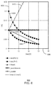
- Fig. 6 is a graph illustrating changes in voltage at the rectifier in terms of current.
- the techniques described herein may be implemented to limit a range of rectified voltage, such as the Vrect 506 of Fig. 5 , based on a supplied current, as indicated at 602.
- Fig. 6 illustrates limiting a range of Vrect 506 between an upper limit 604 associated with an upper limit current, and a lower limit 606 associated with a lower limit current.
- the slope of the line 608 may be adjusted to fit within any desired limit, and the techniques described herein may be implemented with a different higher limit than the 604 and a different lower limit 606.
- Vrect 506 is illustrated in an alternate implementation using a fixed load resistor. As illustrated at 610, the range of voltages within the limits 604 and 606 may be relatively small when compared to the line 608. Further, a digital controlled variable load resistor that may be implement by a set of fixed resistors may require additional components such as an analog to digital converter to sample Vrect, and using a digital portion of the analog to digital converter to tune a digital controlled load resistor for a specific value to meet the limits, as well as a microcontroller to implement the process. In contrast, the techniques described herein include a current source-based compensation logic, such as the current source-based compensation logic 500 of Fig. 5 that may be implemented with relative simplicity.
- Fig. 7 is a time line illustrating changes in voltage at the rectifier in terms of current enabled by a current source.
- the current source-based compensation logic 500 of Fig. 5 may be used to drop a voltage level of rectified voltage, such as the Vx at the external pin 514 of Fig. 5 .
- the Vrect 506 will drop to the desired voltage.
- Vx at the external pin 514 will drop to 1.25 x (Vrect-5) as indicated at 704.
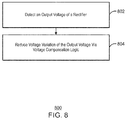
- Fig. 8 is a flow diagram of a method for reducing voltage variation in a rectifier of wireless charging apparatus.
- the method 800 may include detecting an output voltage of a rectifier.
- the method 800 may include reducing a voltage variation of the output voltage via voltage compensation logic.
- reducing voltage variation of the output voltage via voltage comprises driving a voltage controlled capacitor in parallel with a wireless power receiving coil. In some cases, wherein reducing voltage variation of the output voltage via voltage comprises initiating a current source configured to limit a voltage range of the rectifier within a predefined range. In some cases, wherein reducing voltage variation of the output voltage via voltage comprises combination of driving the voltage controlled capacitor and initiating the current source configured to limit a voltage range of the rectifier within a predefined range.
- Limiting the voltage range generates a limit in power range at the rectifier during load modulation of the wireless power receiver.
- Limiting the voltage range via the current source may include generating a first voltage associated with a lower limit of the voltage range at a first amplifier, generating a second voltage associated with a higher limit of the voltage range at a voltage divider, receiving the first voltage and the second voltage at a second amplifier, and providing, from the second amplifier, an equalized output voltage within the predefined range based on the first voltage and the second voltage.
- Reducing the voltage variation via voltage controlled capacitors may include detecting a difference between a reference voltage and a voltage associated with the output from the rectifier, and adjusting a bias voltage output from the difference amplifier to be provided to the voltage controlled capacitor based on the detected difference.
- the bias voltage output from the difference amplifier may be within a predefined continuous range, or may be at discrete levels.
- reducing voltage variation of the output voltage via voltage controlled capacitors may include detecting a difference between a reference voltage and a voltage associated with output from the rectifier, and triggering an associated value in a capacitor bank to reduce capacitance of the voltage controlled capacitor.
- the voltage controlled capacitor is a first voltage controlled capacitor among a second voltage capacitor.
- the second voltage capacitor may be in series with the receiver coil.
- the method may further include configuring the first and second voltage capacitor to provide a minimum operating voltage to the rectifier.
- Example 1 is an apparatus for voltage regulation in a wireless power receiver.
- the wireless charging device may include a rectifier comprising an output voltage, and a means for voltage compensation to reduce voltage variation of the output voltage from the rectifier.
- Example 2 includes the apparatus of example 1.
- the means for voltage compensation may include a voltage controlled capacitor in parallel with a wireless power receiving coil.
- Example 3 includes the apparatus of any combination of examples 1-2.
- the means for voltage compensation generates a compensated current source configured to limit a power range of the rectifier within a predefined range.
- Example 4 includes the apparatus of any combination of examples 1-3.
- limiting the power range is a function of voltage range during load modulation of the wireless power receiver.
- Example 5 includes the apparatus of any combination of examples 1-4.
- the current source may include a first amplifier to generate a first voltage associated with a lower limit of the voltage range, a voltage divider to generate a second voltage associated with a higher limit of the voltage range, a second amplifier to: receive the first voltage and the second voltage, and supply an equalized output voltage within the predefined range based on the first voltage and the second voltage.
- Example 6 includes the apparatus of any combination of examples 1-5.
- the voltage comparison logic may include a voltage controlled capacitor, a difference amplifier configured to: detect a difference between a reference voltage and a voltage associated with the output from the rectifier, and adjust a bias voltage output from the difference amplifier supplied to the voltage controlled capacitor based on the detected difference.
- Example 7 includes the apparatus of any combination of examples 1-6.
- the bias voltage output from the difference amplifier is within a predefined continuous range.
- Example 8 includes the apparatus of any combination of examples 1-7.
- the voltage controlled capacitor is a first voltage controlled capacitor.
- This example includes a second voltage controlled capacitor in series with the receiver coil, and wherein the first voltage controlled capacitor and the second voltage controlled capacitor are configured to supply a minimum operating voltage to the rectifier.
- Example 9 includes the apparatus of any combination of examples 1-8.
- the voltage comparison logic may include a difference amplifier configured to: detect a difference between a reference voltage and a voltage associated with output from the rectifier, and trigger an associated value in a capacitor bank to reduce capacitance of the voltage controlled capacitor.
- Example 10 includes the apparatus of any combination of examples 1-9.
- a bias voltage output from the difference amplifier is within a predefined range of discrete voltages.
- Example 11 is a method for voltage regulation in a wireless power receiver.
- the wireless charging device may include detecting an output voltage of a rectifier, and reducing voltage variation of the output voltage via voltage compensation logic.
- Example 12 includes the method of example 11.
- reducing voltage variation of the output voltage via voltage may include driving a voltage controlled capacitor in parallel with a wireless power receiving coil.
- Example 13 includes the method of any combination of examples 11-12. This example includes limiting a power range of the rectifier within a predefined range as a function of rectified voltage.
- Example 14 includes the method of any combination of examples 11-13.
- the power range is limited during load modulation of the wireless power receiver.
- Example 15 includes the method of any combination of examples 11-14.
- limiting the voltage range via the current source may include generating a first voltage associated with a lower limit of the voltage range at a first amplifier, generating a second voltage associated with a higher limit of the voltage range at a voltage divider, receiving the first voltage and the second voltage at a second amplifier, and providing, from the second amplifier, an equalized output voltage within the predefined range based on the first voltage and the second voltage.
- Example 16 includes the method of any combination of examples 11-15.
- reducing voltage variation of the output voltage via voltage controlled capacitors may include detecting a difference between a reference voltage and a voltage associated with the output from the rectifier, and adjusting a bias voltage output from the difference amplifier to be provided to the voltage controlled capacitor based on the detected difference.
- Example 17 includes the method of any combination of examples 11-16.
- the bias voltage output from the difference amplifier is within a predefined continuous range.
- Example 18 includes the method of any combination of examples 11-17.
- the voltage controlled capacitor is a first voltage controlled capacitor among a second voltage capacitor, the second voltage capacitor in series with the receiver coil, the method further comprising configuring the first and second voltage capacitor to provide a minimum operating voltage to the rectifier.
- Example 19 includes the method of any combination of examples 11-18.
- T reducing voltage variation of the output voltage via voltage controlled capacitors may include detecting a difference between a reference voltage and a voltage associated with output from the rectifier, and triggering an associated value in a capacitor bank to reduce capacitance of the voltage controlled capacitor.
- Example 20 includes the method of any combination of examples 11-19.
- a bias voltage output from the difference amplifier is within a predefined range of discrete voltages.
- Example 21 is a system for wireless charging.
- the wireless charging device may include a rectifier comprising an output voltage, and voltage compensation logic to reduce voltage variation of the output voltage from the rectifier.
- Example 22 includes the system of example 21.
- the means for voltage compensation may include a voltage controlled capacitor in parallel with a wireless power receiving coil.
- Example 23 includes the system of any combination of examples 21-22.
- the means for voltage compensation generates a compensated current source configured to limit a power range of the rectifier within a predefined range.
- Example 24 includes the system of any combination of examples 21 - 23.
- limiting the power range is a function of voltage range during load modulation of the wireless power receiver.
- Example 25 includes the system of any combination of examples 21 - 24.
- the current source may include a first amplifier to generate a first voltage associated with a lower limit of the voltage range, a voltage divider to generate a second voltage associated with a higher limit of the voltage range, a second amplifier to: receive the first voltage and the second voltage, and supply an equalized output voltage within the predefined range based on the first voltage and the second voltage.
- Example 26 includes the system of any combination of examples 21 - 25.
- the voltage comparison logic may include a voltage controlled capacitor, a difference amplifier configured to: detect a difference between a reference voltage and a voltage associated with the output from the rectifier, and adjust a bias voltage output from the difference amplifier supplied to the voltage controlled capacitor based on the detected difference.
- Example 27 includes the system of any combination of examples 21 - 26.
- the bias voltage output from the difference amplifier is within a predefined continuous range.
- Example 28 includes the system of any combination of examples 21 - 27.
- the voltage controlled capacitor is a first voltage controlled capacitor.
- This example includes a second voltage controlled capacitor in series with the receiver coil, and wherein the first voltage controlled capacitor and the second voltage controlled capacitor are configured to supply a minimum operating voltage to the rectifier.
- Example 29 includes the system of any combination of examples 21 - 28.
- the voltage comparison logic may include a difference amplifier configured to: detect a difference between a reference voltage and a voltage associated with output from the rectifier, and trigger an associated value in a capacitor bank to reduce capacitance of the voltage controlled capacitor.
- Example 30 includes the system of any combination of examples 21 - 29.
- a bias voltage output from the difference amplifier is within a predefined range of discrete voltages.
- Example 31 is an apparatus for voltage regulation in a wireless power receiver.
- the wireless charging device may include a rectifier comprising an output voltage, and a means for voltage compensation to reduce voltage variation of the output voltage from the rectifier.
- Example 32 includes the apparatus of example 31.
- the means for voltage compensation may include a voltage controlled capacitor in parallel with a wireless power receiving coil.
- Example 33 includes the apparatus of any combination of examples 31-32.
- the means for voltage compensation generates a compensated current source configured to limit a power range of the rectifier within a predefined range.
- Example 34 includes the apparatus of any combination of examples 31-33.
- limiting the power range is a function of voltage range during load modulation of the wireless power receiver.
- Example 35 includes the apparatus of any combination of examples 31-34.
- the current source may include a first amplifier to generate a first voltage associated with a lower limit of the voltage range, a voltage divider to generate a second voltage associated with a higher limit of the voltage range, a second amplifier to: receive the first voltage and the second voltage, and supply an equalized output voltage within the predefined range based on the first voltage and the second voltage.
- Example 36 includes the apparatus of any combination of examples 31-35.
- the voltage comparison logic may include a voltage controlled capacitor, a difference amplifier configured to: detect a difference between a reference voltage and a voltage associated with the output from the rectifier, and adjust a bias voltage output from the difference amplifier supplied to the voltage controlled capacitor based on the detected difference.
- Example 37 includes the apparatus of any combination of examples 31-36.
- the bias voltage output from the difference amplifier is within a predefined continuous range.
- Example 38 includes the apparatus of any combination of examples 31-37.
- the voltage controlled capacitor is a first voltage controlled capacitor.
- This example includes a second voltage controlled capacitor in series with the receiver coil, and wherein the first voltage controlled capacitor and the second voltage controlled capacitor are configured to supply a minimum operating voltage to the rectifier.
- Example 39 includes the apparatus of any combination of examples 31-38.
- the voltage comparison logic may include a difference amplifier configured to: detect a difference between a reference voltage and a voltage associated with output from the rectifier, and trigger an associated value in a capacitor bank to reduce capacitance of the voltage controlled capacitor.
- Example 40 includes the apparatus of any combination of examples 31-39.
- a bias voltage output from the difference amplifier is within a predefined range of discrete voltages.
- Example 41 is a method for voltage regulation in a wireless power receiver.
- the wireless charging device may include detecting an output voltage of a rectifier, and reducing voltage variation of the output voltage via voltage compensation logic.
- Example 42 includes the method of example 41.
- reducing voltage variation of the output voltage via voltage may include driving a voltage controlled capacitor in parallel with a wireless power receiving coil.
- Example 43 includes the method of any combination of examples 41 - 42. This example includes limiting a power range of the rectifier within a predefined range as a function of rectified voltage.
- Example 44 includes the method of any combination of examples 41 - 43.
- the power range is limited during load modulation of the wireless power receiver.
- Example 45 includes the method of any combination of examples 41 - 44.
- limiting the voltage range via the current source may include generating a first voltage associated with a lower limit of the voltage range at a first amplifier, generating a second voltage associated with a higher limit of the voltage range at a voltage divider, receiving the first voltage and the second voltage at a second amplifier, and providing, from the second amplifier, an equalized output voltage within the predefined range based on the first voltage and the second voltage.
- Example 46 includes the method of any combination of examples 41 - 45.
- reducing voltage variation of the output voltage via voltage controlled capacitors may include detecting a difference between a reference voltage and a voltage associated with the output from the rectifier, and adjusting a bias voltage output from the difference amplifier to be provided to the voltage controlled capacitor based on the detected difference.
- Example 47 includes the method of any combination of examples 41 - 46.
- the bias voltage output from the difference amplifier is within a predefined continuous range.
- Example 48 includes the method of any combination of examples 41 - 47.
- the voltage controlled capacitor is a first voltage controlled capacitor among a second voltage capacitor, the second voltage capacitor in series with the receiver coil, the method further comprising configuring the first and second voltage capacitor to provide a minimum operating voltage to the rectifier.
- Example 49 includes the method of any combination of examples 41 - 48.
- T reducing voltage variation of the output voltage via voltage controlled capacitors may include detecting a difference between a reference voltage and a voltage associated with output from the rectifier, and triggering an associated value in a capacitor bank to reduce capacitance of the voltage controlled capacitor.
- Example 50 includes the method of any combination of examples 41 - 49.
- a bias voltage output from the difference amplifier is within a predefined range of discrete voltages.
- the elements in some cases may each have a same reference number or a different reference number to suggest that the elements represented could be different and/or similar.
- an element may be flexible enough to have different implementations and work with some or all of the systems shown or described herein.
- the various elements shown in the figures may be the same or different. Which one is referred to as a first element and which is called a second element is arbitrary.
Landscapes
- Engineering & Computer Science (AREA)
- Power Engineering (AREA)
- Computer Networks & Wireless Communication (AREA)
- Life Sciences & Earth Sciences (AREA)
- Sustainable Development (AREA)
- Sustainable Energy (AREA)
- Transportation (AREA)
- Mechanical Engineering (AREA)
- Charge And Discharge Circuits For Batteries Or The Like (AREA)
- Rectifiers (AREA)
- Dc-Dc Converters (AREA)
Abstract
Description
- This disclosure relates generally to techniques for wireless charging. Specifically, this disclosure relates to regulation of voltage in wireless power systems.
- A basic wireless charging system may include a wireless power transmitter unit (PTU) and a wireless power receiving unit (PRU). For example, a PTU may include a transmit (Tx) coil, and a PRU may include receive (Rx) coil. Magnetic resonance wireless charging may employ a magnetic coupling between the Tx coil and the Rx coil. In some cases, wireless power received may vary causing issues with efficiency in wireless charging systems. In some cases, variations of voltage may violate wireless charging standard specifications.
-
-
Fig. 1 is block diagram of a PTU to provide power to a PRU, wherein the includes logic configured to reduce variations in voltage; -
Fig. 2 is an illustration of logic configured to reduce variations of rectifier voltage; -
Fig. 3 is a graph illustrating changes in voltage in terms of capacitance; -
Fig. 4 is a graph illustrating changes in rectifier voltage in terms of resistance in a magnetic coupling between a wireless transmitter and a wireless receiver; -
Fig. 5 is an illustration of logic configured to reduce variations of rectifier power using a compensated current source that may change as a function of rectified voltage; -
Fig. 6 is a graph illustrating changes in voltage at the rectifier in terms of current; -
Fig. 7 is a time line illustrating changes in voltage at the rectifier in terms of current enabled by a current source; and -
Fig. 8 is a flow diagram of a method for reducing voltage variation in a rectifier of wireless charging apparatus. - The same numbers are used throughout the disclosure and the figures to reference like components and features. Numbers in the 100 series refer to features originally found in
Fig. 1 ; numbers in the 200 series refer to features originally found inFig. 2 ; and so on. - The present disclosure relates generally to techniques for wireless charging. Specifically, the techniques described herein include a wireless power rectifier and voltage compensation logic to reduce voltage variation of output voltage from the rectifier. As discussed above, voltage variations may generate inefficiencies in wireless charging. For example, spatial freedom of placement of a device under charge having a receiver (Rx) coil may result in a potentially large rectified receiver voltage (Vrect) variation. Variations in Vrect may constrain designs by requiring stringent field uniformity in some cases.
- Voltage compensation logic, as referred to herein, includes one or more electric circuit components, modules, or integrated components configured to reduce variation in voltage. Specifically, voltage compensation logic may be configured to reduce variation of Vrect at a wireless charging component such as a wireless charging receiving coil. As discussed in more detail below, voltage compensation logic may include one or more of capacitors in a feedback loop configured to reduce variations in Vrect, amplifiers, resistors, and the like.
- In some cases, large variation on Vrect may present different design challenges, as discussed below in regard to
Fig. 2 - Fig. 4 . One design challenge may include delivering load modulation signals within a predefined range. For example, in some cases power (Prect) of load modulation may be required to be between .5 watts (W) and 1.1 W. Therefore, in some cases, the voltage compensation logic and techniques discussed herein may generate a compensated current source (I_compensate) that may be used to toggle load modulation signaling on Vrect (for any Vrect, for example Vrect = 4Volts-20Volts), wherein .5W<Prect = Vrect*I_compensate < 1.1W, as discussed in more detail below in regard toFigs. 5-7 . - In some cases, the techniques discussed herein may be implemented using a wireless charging standard protocol, such as the specification provided by Alliance For Wireless Power (A4WP) version 1.2.1, May 07, 2014. A wireless power Rx coil may be a component in a power receiving unit (PRU), while a wireless power transmission (Tx) coil may be a component in a power transmitting unit (PTU), as discussed in more detail below. However, the techniques described herein may be implemented using any other wireless charging standard protocol where applicable.
-
Fig. 1 is block diagram of a PTU to provide power to a PRU, wherein a magnetic component protrudes from the PTU. A PTU 102 may couple to a PRU 104 via magnetic inductive coupling betweenresonators 106, and108, as indicated by thearrow 110. Theresonator 106 may be referred to herein as aTx coil 106 of thePTU 102. Theresonator 108 may be referred to herein as anRx coil 108 of the PRU 104. - As illustrated in
Fig. 1 , the PRU 104 may includelogic 112. Thelogic 112 may be referred to herein asvoltage compensation logic 112. Thevoltage compensation logic 112 may be configured as an integrated component of arectifier 114, as a separate component of therectifier 114, or any combination thereof. In any case, thevoltage compensation logic 112 may be configured to reduce variations in Vrect. In other words, thevoltage compensation logic 112 may be configured to reduce variations in rectified voltage output by therectifier 114. Thevoltage compensation logic 112 may be composed of one or more components, such as electronic circuit components, as discussed in more detail below in regard toFig. 2 andFig. 5 . For example, thevoltage compensation logic 112 may be implemented as a current source to introduce limits on Vrect variation. As another example, thevoltage compensation logic 112 may be implemented using a voltage controlled capacitor in parallel with theRx coil 108. Additional details are discussed in more detail below in regard toFig. 2 andFig. 5 , as well as throughout the present description, Figures, and claims. - In
Fig. 1 , the PRU 104 may include acontroller 116 configured to detect current received at theRx coil 108 resulting from an inductive coupling between theTx coil 106 and theRx coil 108. In some cases, thecontroller 114 may be configured to initiate load modulations to communicate a wireless data broadcast. - In some cases, the wireless broadcast may be carried out by a wireless data transmission component such as a Bluetooth Low Energy (BLE)
module 118. In some cases, the wireless data transmission component may be integrated as operations of thecontroller 116, aload modulation circuit 120, a direct current to direct current (DC2DC)converter 122, or any combination thereof, wherein the data transmission may be indicated by patterns in the load modulation. - As illustrated in
Fig. 1 , theDC2DC converter 122 provides a DC output to abattery 124, or another current/power consuming component. TheDC2DC converter 122 may convert DC received as a result of the inductive coupling of theTx coil 106, theRx coil 108, and therectifier 114. - The
PTU 102 may include aBLE module 126 configured to communicate with theBLE module 118. ThePTU 102 may also include acurrent sensor 128, acontroller 130, apower amplifier 132, aDC2DC converter 134, anoscillator 136, and amatching network 138. Thecurrent sensor 128 may be an ampere meter, a volt meter, or any other sensor configured to sense load variations occurring due to inductive coupling between thePTU 102 and another object, such as the PRU 104. Thecurrent sensor 128 may provide an indication of load change to thecontroller 130 of thePTU 102. Thecontroller 130 may power on thepower amplifier 132 configured to receive direct current (DC) from theDC2DC converter 134, and to amplify and oscillate the current. Anoscillator 136 may oscillate the power provided at a given frequency and amatching network 138 may be used to match the amplified oscillation provided to theresonator 106 of thePTU 102. - The block diagram of
Fig. 1 is not intended to indicate that thePTU 102 and/or thePRU 104 are to include all of the components shown inFig. 1 . Further, thePTU 102 and/or thePRU 104 may include any number of additional components not shown inFig. 1 , depending on the details of the specific implementation. -
Fig. 2 is an illustration of logic configured to reduce variations of rectifier voltage. The logic, generally indicated at 200, is one implementation of thevoltage compensation logic 112 ofFig. 1 . InFig. 2 a voltage controlledcapacitor 202 may be coupled in parallel to an Rx coil, such as theRx coil 108 ofFig. 1 . TheRx coil 108 may be configured to be inductively coupled to a Tx coil, such as theTx coil 106 ofFig. 1 , as illustrated by the coupling Z21 204ofFig. 2 . A rectifier, such as therectifier 114 ofFig. 1 , may output a voltage indicated byVrect 208 inFig. 2 . - A voltage divider, indicated at the dashed
circle 206, may be configured to sampleVrect 208 and to reduceVrect 208 to a fraction so thatVrect 208 is comparable to a reference voltage (Vref) 210. A difference amplifier 212 may be configured to detect a difference betweenVref 210 and the divided voltage level ofVrect 208. A bias voltage indicated at 214 may be adjusted based on the detected difference. Thebias voltage 214 is proportional to the difference between theVref 210 and theVrect 208. Thebias voltage 214 may drive the voltage controlledcapacitor 202 to change the capacitance of the voltage controlledcapacitor 202. - The
voltage divider 206 andVref 210 may be chosen such that asVrect 208 increases above a predefined value for theVref 210, thebias voltage 214 supplied to the voltage controlledcapacitor 202 increases. An increase in voltage supplied by thebias voltage 214 to the voltage controlledcapacitor 202 may reduce the capacitance of the voltage controlledcapacitor 202, and therefore a reduction of output voltage, such as theVrect 208 may result. The voltage controlledcapacitor 202 may thereby introduce a continuous limit to voltage values occurring atVrect 208. The limitation of the voltage range ofVrect 208 may enable compliance with standards specifications for wireless charging, such as limitations to voltage ranges implemented by A4WP discussed above during Long Beacon Extension Requests (LEBRs) wherein a PRU, such as thePRU 104 may be limited to load variations of .5 watts and 1.1 watts as discussed in more detail below in regard toFig. 5 . - In some cases, the voltage controlled
capacitor 202 may be capacitor bank comprising a plurality of capacitors having discrete capacitance value capabilities. In this scenario, an increase ofVrect 208 may trigger appropriate values in the capacitor bank to reduce net capacitance of the capacitor bank, thereby reducingvoltage including Vrect 208. - It may be useful to note variations of the implementation of
Fig. 2 . For example, the difference amplifier 212 may be replaced with a comparator that provides input to a microcontroller, or an interrupt driven adjustable voltage source configured to adjust capacitance as appropriate. A combination of fixed and variable capacitors may also be used to tailor a capacitive range of a variable capacitor to a larger total capacitance adjustment. - As illustrated in
Fig. 1 , acapacitor 216 may also be included in thelogic 200 wherein thecapacitor 216 is in series with theRx coil 108. In some cases, thecapacitor 216 may be a tunable capacitor, such as the voltage controlledcapacitor 202. In this scenario, a finer granularity of voltage regulation may be approached than if thecapacitor 216 was not tunable. The configuration of thecapacitor 216 and the voltage controlledcapacitor 202 may be based on an operating set voltage at aminimum Z 21 204 inductive coupling. -
Fig. 3 is a graph illustrating changes in voltage in terms of capacitance. As discussed above, changes in capacitance may result in changes in voltage. As illustrated inFig. 3 , as capacitance increases at 302, a bias voltage decreases at 304. Further, as capacitance decreases at 302, voltage increases at 304. The techniques described herein include capacitance-based voltage compensation logic, according to one aspect. -
Fig. 4 is a graph illustrating changes in rectifier voltage in terms of magnetic coupling (represented by Z21 in ohms on the horizontal axis) between a wireless transmitter and a wireless receiver. As discussed above, when variation of coupling occurs, such as variation ofZ 21 204 ofFig. 2 , a rectifier voltage variation inVrect 208 may result. As indicated atline 402, the voltage ofVrect 208 varies widely as the coupling inZ 21 204 also varies. However, when the capacitance is tunable, as Z21 increases theVrect 208 may be maintained at the same level. -
Fig. 5 is an illustration of logic configured to reduce variations of rectifier power using a compensated current source that may be changed as a function of Vrect. As discussed above, in some cases, one design challenge may include delivering load modulation signals within a predefined range. For example, in some cases power (Prect) of load modulation may be required to be between .5 watts (W) and 1.1 W. Therefore, in some cases, the voltage compensation logic and techniques discussed herein may generate a compensated current source (I_compensate) that may be used to toggle load modulation signaling on Vrect (for any Vrect, for example Vrect = 4Volts-20Volts), wherein .5W<Prect = Vrect*I_compensate < 1.1W, as discussed in more detail below in regard toFigs. 5-7 . - The logic, generally indicated at 500, is one implementation of the
voltage compensation logic 112 ofFig. 1 . Thelogic 500 may be referred to herein as current source-basedvoltage compensation logic 500. InFig. 5 , thelogic 500 includes afirst amplifier 502, asecond amplifier 504, communicatively coupled to a rectified voltage (Vrect) 506. Thefirst amplifier 502 may be configured to receive an input reference voltage (Vref) 508. TheVrect 506 andVref 508 may be similar to theVrect 208 and theVref 210 ofFig. 2 , respectively. Theexample logic 500 may be implemented alone, or in any combination with thelogic 200 ofFig. 2 . - As illustrated in
Fig. 5 , thefirst amplifier 502 may be configured to drive a current "/" on a first resistor (R1) 510 having a resistance "R". In the example illustrated inFig. 5 ,Vref 508 is equal to 5 volts (V), and the current / may be equal to .5 Volts/R. The current / may generate a voltage of Vrect-5V on a negative input of thesecond amplifier 504, as indicated at 512. Thelogic 500 may include anexternal pin 514. Voltage on the external pin may be indicated by "Vx." The voltage Vx may be determined byEquation 1 below:
- In Eq. 1, "VR5" represents the difference in voltage between the rectified voltage Vrect and the voltage Vx at the
external pin 514 of thelogic 500. The behavior of Vx may be a function of an output signal of thesecond amplifier 504. A voltage divider, generally indicated at 516, may generate a fraction (4Vx/5) of the voltage Vx on a positive input to the second amplifier, as indicated at 518. Thesecond amplifier 504 may be configured to equalize the voltage on the positive line at 518 and the voltage on thenegative line 512 as illustrated inEquation 2 below:

- In the example illustrated in
Fig. 5 , placing resistor R5 equal to 50 Ohm, a current load Iload will result, as illustrated in Equation 4 below:
- Although
Fig. 5 implements specific values such as 50 ohm on R5, Vrect-5 oninput line 512, 4Vx/5 oninput line 518, a Vref of .5 V, and the like, any values may be used to produce a desired limit onVrect 506. The techniques described herein implement current source-basedvoltage compensation logic 500. In some cases, the current source-basedcompensation logic 500 may be used to restrict Vrect during certain modes of operation. - For example, the A4WP standards specification includes an initialization flow wherein a PTU, such as the
PTU 102 ofFig. 1 , sends a periodic power beacon (long beacon) that may occur for 100 milliseconds. During the long beacon, a PRU, such as thePRU 104 ofFig. 1 , may respond with a BLE advertisement signal, or a Long Beacon Extension Request (LBER) signal based on a load modulation signature. The LBER signal may include two modulation pulses at 100 hertz (Hz). During a positive edge of the load modulation pulse, thePRU 104 may be required to sink at least .5 Watts of power, and not more than 1.1 Watts. Therefore, the techniques described herein may be useful for limiting voltage, and therefore power, during such load modulation processes. -
Fig. 6 is a graph illustrating changes in voltage at the rectifier in terms of current. As discussed above, the techniques described herein may be implemented to limit a range of rectified voltage, such as theVrect 506 ofFig. 5 , based on a supplied current, as indicated at 602. As one example,Fig. 6 illustrates limiting a range ofVrect 506 between anupper limit 604 associated with an upper limit current, and alower limit 606 associated with a lower limit current. A resulting current 608 may be represented by Equation 4 below:
line 608 may be adjusted to fit within any desired limit, and the techniques described herein may be implemented with a different higher limit than the 604 and a differentlower limit 606. At 610,Vrect 506 is illustrated in an alternate implementation using a fixed load resistor. As illustrated at 610, the range of voltages within thelimits line 608. Further, a digital controlled variable load resistor that may be implement by a set of fixed resistors may require additional components such as an analog to digital converter to sample Vrect, and using a digital portion of the analog to digital converter to tune a digital controlled load resistor for a specific value to meet the limits, as well as a microcontroller to implement the process. In contrast, the techniques described herein include a current source-based compensation logic, such as the current source-basedcompensation logic 500 ofFig. 5 that may be implemented with relative simplicity. -
Fig. 7 is a time line illustrating changes in voltage at the rectifier in terms of current enabled by a current source. As discussed above, the current source-basedcompensation logic 500 ofFig. 5 may be used to drop a voltage level of rectified voltage, such as the Vx at theexternal pin 514 ofFig. 5 . When thesecond amplifier 504 ofFig. 5 is enabled at 702, theVrect 506 will drop to the desired voltage. In this example, Vx at theexternal pin 514 will drop to 1.25 x (Vrect-5) as indicated at 704. -
Fig. 8 is a flow diagram of a method for reducing voltage variation in a rectifier of wireless charging apparatus. At 802, themethod 800 may include detecting an output voltage of a rectifier. Atblock 804, themethod 800 may include reducing a voltage variation of the output voltage via voltage compensation logic. - In some cases, reducing voltage variation of the output voltage via voltage comprises driving a voltage controlled capacitor in parallel with a wireless power receiving coil. In some cases, wherein reducing voltage variation of the output voltage via voltage comprises initiating a current source configured to limit a voltage range of the rectifier within a predefined range. In some cases, wherein reducing voltage variation of the output voltage via voltage comprises combination of driving the voltage controlled capacitor and initiating the current source configured to limit a voltage range of the rectifier within a predefined range.
- Further, in some cases limiting the voltage range generates a limit in power range at the rectifier during load modulation of the wireless power receiver. Limiting the voltage range via the current source may include generating a first voltage associated with a lower limit of the voltage range at a first amplifier, generating a second voltage associated with a higher limit of the voltage range at a voltage divider, receiving the first voltage and the second voltage at a second amplifier, and providing, from the second amplifier, an equalized output voltage within the predefined range based on the first voltage and the second voltage.
- Reducing the voltage variation via voltage controlled capacitors may include detecting a difference between a reference voltage and a voltage associated with the output from the rectifier, and adjusting a bias voltage output from the difference amplifier to be provided to the voltage controlled capacitor based on the detected difference. The bias voltage output from the difference amplifier may be within a predefined continuous range, or may be at discrete levels. In the latter case, reducing voltage variation of the output voltage via voltage controlled capacitors may include detecting a difference between a reference voltage and a voltage associated with output from the rectifier, and triggering an associated value in a capacitor bank to reduce capacitance of the voltage controlled capacitor.
- Further, in some cases, the voltage controlled capacitor is a first voltage controlled capacitor among a second voltage capacitor. The second voltage capacitor may be in series with the receiver coil. The method may further include configuring the first and second voltage capacitor to provide a minimum operating voltage to the rectifier.
- Example 1 is an apparatus for voltage regulation in a wireless power receiver. In this example, the wireless charging device may include a rectifier comprising an output voltage, and a means for voltage compensation to reduce voltage variation of the output voltage from the rectifier.
- Example 2 includes the apparatus of example 1. In this example, the means for voltage compensation may include a voltage controlled capacitor in parallel with a wireless power receiving coil.
- Example 3 includes the apparatus of any combination of examples 1-2. In this example, the means for voltage compensation generates a compensated current source configured to limit a power range of the rectifier within a predefined range.
- Example 4 includes the apparatus of any combination of examples 1-3. In this example limiting the power range is a function of voltage range during load modulation of the wireless power receiver.
- Example 5 includes the apparatus of any combination of examples 1-4. In this example, the current source may include a first amplifier to generate a first voltage associated with a lower limit of the voltage range, a voltage divider to generate a second voltage associated with a higher limit of the voltage range, a second amplifier to: receive the first voltage and the second voltage, and supply an equalized output voltage within the predefined range based on the first voltage and the second voltage.
- Example 6 includes the apparatus of any combination of examples 1-5. In this example, the voltage comparison logic may include a voltage controlled capacitor, a difference amplifier configured to: detect a difference between a reference voltage and a voltage associated with the output from the rectifier, and adjust a bias voltage output from the difference amplifier supplied to the voltage controlled capacitor based on the detected difference.
- Example 7 includes the apparatus of any combination of examples 1-6. In this example, the bias voltage output from the difference amplifier is within a predefined continuous range.
- Example 8 includes the apparatus of any combination of examples 1-7. In this example, the voltage controlled capacitor is a first voltage controlled capacitor. This example includes a second voltage controlled capacitor in series with the receiver coil, and wherein the first voltage controlled capacitor and the second voltage controlled capacitor are configured to supply a minimum operating voltage to the rectifier.
- Example 9 includes the apparatus of any combination of examples 1-8. In this example, the voltage comparison logic may include a difference amplifier configured to: detect a difference between a reference voltage and a voltage associated with output from the rectifier, and trigger an associated value in a capacitor bank to reduce capacitance of the voltage controlled capacitor.
- Example 10 includes the apparatus of any combination of examples 1-9. In this example a bias voltage output from the difference amplifier is within a predefined range of discrete voltages.
- Example 11 is a method for voltage regulation in a wireless power receiver. In this example, the wireless charging device may include detecting an output voltage of a rectifier, and reducing voltage variation of the output voltage via voltage compensation logic.
- Example 12 includes the method of example 11. In this example reducing voltage variation of the output voltage via voltage may include driving a voltage controlled capacitor in parallel with a wireless power receiving coil.
- Example 13 includes the method of any combination of examples 11-12. This example includes limiting a power range of the rectifier within a predefined range as a function of rectified voltage.
- Example 14 includes the method of any combination of examples 11-13. In this example, the power range is limited during load modulation of the wireless power receiver.
- Example 15 includes the method of any combination of examples 11-14. In this example limiting the voltage range via the current source may include generating a first voltage associated with a lower limit of the voltage range at a first amplifier, generating a second voltage associated with a higher limit of the voltage range at a voltage divider, receiving the first voltage and the second voltage at a second amplifier, and providing, from the second amplifier, an equalized output voltage within the predefined range based on the first voltage and the second voltage.
- Example 16 includes the method of any combination of examples 11-15. In this example reducing voltage variation of the output voltage via voltage controlled capacitors may include detecting a difference between a reference voltage and a voltage associated with the output from the rectifier, and adjusting a bias voltage output from the difference amplifier to be provided to the voltage controlled capacitor based on the detected difference.
- Example 17 includes the method of any combination of examples 11-16. In this example, the bias voltage output from the difference amplifier is within a predefined continuous range.
- Example 18 includes the method of any combination of examples 11-17. In this example, the voltage controlled capacitor is a first voltage controlled capacitor among a second voltage capacitor, the second voltage capacitor in series with the receiver coil, the method further comprising configuring the first and second voltage capacitor to provide a minimum operating voltage to the rectifier.
- Example 19 includes the method of any combination of examples 11-18. T reducing voltage variation of the output voltage via voltage controlled capacitors may include detecting a difference between a reference voltage and a voltage associated with output from the rectifier, and triggering an associated value in a capacitor bank to reduce capacitance of the voltage controlled capacitor.
- Example 20 includes the method of any combination of examples 11-19. In this example a bias voltage output from the difference amplifier is within a predefined range of discrete voltages.
- Example 21 is a system for wireless charging. In this example, the wireless charging device may include a rectifier comprising an output voltage, and voltage compensation logic to reduce voltage variation of the output voltage from the rectifier.
- Example 22 includes the system of example 21. In this example, the means for voltage compensation may include a voltage controlled capacitor in parallel with a wireless power receiving coil.
- Example 23 includes the system of any combination of examples 21-22. In this example, the means for voltage compensation generates a compensated current source configured to limit a power range of the rectifier within a predefined range.
- Example 24 includes the system of any combination of examples 21 - 23. In this example limiting the power range is a function of voltage range during load modulation of the wireless power receiver.
- Example 25 includes the system of any combination of examples 21 - 24. In this example, the current source may include a first amplifier to generate a first voltage associated with a lower limit of the voltage range, a voltage divider to generate a second voltage associated with a higher limit of the voltage range, a second amplifier to: receive the first voltage and the second voltage, and supply an equalized output voltage within the predefined range based on the first voltage and the second voltage.
- Example 26 includes the system of any combination of examples 21 - 25. In this example, the voltage comparison logic may include a voltage controlled capacitor, a difference amplifier configured to: detect a difference between a reference voltage and a voltage associated with the output from the rectifier, and adjust a bias voltage output from the difference amplifier supplied to the voltage controlled capacitor based on the detected difference.
- Example 27 includes the system of any combination of examples 21 - 26. In this example, the bias voltage output from the difference amplifier is within a predefined continuous range.
- Example 28 includes the system of any combination of examples 21 - 27. In this example, the voltage controlled capacitor is a first voltage controlled capacitor. This example includes a second voltage controlled capacitor in series with the receiver coil, and wherein the first voltage controlled capacitor and the second voltage controlled capacitor are configured to supply a minimum operating voltage to the rectifier.
- Example 29 includes the system of any combination of examples 21 - 28. In this example, the voltage comparison logic may include a difference amplifier configured to: detect a difference between a reference voltage and a voltage associated with output from the rectifier, and trigger an associated value in a capacitor bank to reduce capacitance of the voltage controlled capacitor.
- Example 30 includes the system of any combination of examples 21 - 29. In this example a bias voltage output from the difference amplifier is within a predefined range of discrete voltages.
- Example 31 is an apparatus for voltage regulation in a wireless power receiver. In this example, the wireless charging device may include a rectifier comprising an output voltage, and a means for voltage compensation to reduce voltage variation of the output voltage from the rectifier.
- Example 32 includes the apparatus of example 31. In this example, the means for voltage compensation may include a voltage controlled capacitor in parallel with a wireless power receiving coil.
- Example 33 includes the apparatus of any combination of examples 31-32. In this example, the means for voltage compensation generates a compensated current source configured to limit a power range of the rectifier within a predefined range.
- Example 34 includes the apparatus of any combination of examples 31-33. In this example limiting the power range is a function of voltage range during load modulation of the wireless power receiver.
- Example 35 includes the apparatus of any combination of examples 31-34. In this example, the current source may include a first amplifier to generate a first voltage associated with a lower limit of the voltage range, a voltage divider to generate a second voltage associated with a higher limit of the voltage range, a second amplifier to: receive the first voltage and the second voltage, and supply an equalized output voltage within the predefined range based on the first voltage and the second voltage.
- Example 36 includes the apparatus of any combination of examples 31-35. In this example, the voltage comparison logic may include a voltage controlled capacitor, a difference amplifier configured to: detect a difference between a reference voltage and a voltage associated with the output from the rectifier, and adjust a bias voltage output from the difference amplifier supplied to the voltage controlled capacitor based on the detected difference.
- Example 37 includes the apparatus of any combination of examples 31-36. In this example, the bias voltage output from the difference amplifier is within a predefined continuous range.
- Example 38 includes the apparatus of any combination of examples 31-37. In this example, the voltage controlled capacitor is a first voltage controlled capacitor. This example includes a second voltage controlled capacitor in series with the receiver coil, and wherein the first voltage controlled capacitor and the second voltage controlled capacitor are configured to supply a minimum operating voltage to the rectifier.
- Example 39 includes the apparatus of any combination of examples 31-38. In this example, the voltage comparison logic may include a difference amplifier configured to: detect a difference between a reference voltage and a voltage associated with output from the rectifier, and trigger an associated value in a capacitor bank to reduce capacitance of the voltage controlled capacitor.
- Example 40 includes the apparatus of any combination of examples 31-39. In this example a bias voltage output from the difference amplifier is within a predefined range of discrete voltages.
- Example 41 is a method for voltage regulation in a wireless power receiver. In this example, the wireless charging device may include detecting an output voltage of a rectifier, and reducing voltage variation of the output voltage via voltage compensation logic.
- Example 42 includes the method of example 41. In this example reducing voltage variation of the output voltage via voltage may include driving a voltage controlled capacitor in parallel with a wireless power receiving coil.
- Example 43 includes the method of any combination of examples 41 - 42. This example includes limiting a power range of the rectifier within a predefined range as a function of rectified voltage.
- Example 44 includes the method of any combination of examples 41 - 43. In this example, the power range is limited during load modulation of the wireless power receiver.
- Example 45 includes the method of any combination of examples 41 - 44. In this example limiting the voltage range via the current source may include generating a first voltage associated with a lower limit of the voltage range at a first amplifier, generating a second voltage associated with a higher limit of the voltage range at a voltage divider, receiving the first voltage and the second voltage at a second amplifier, and providing, from the second amplifier, an equalized output voltage within the predefined range based on the first voltage and the second voltage.
- Example 46 includes the method of any combination of examples 41 - 45. In this example reducing voltage variation of the output voltage via voltage controlled capacitors may include detecting a difference between a reference voltage and a voltage associated with the output from the rectifier, and adjusting a bias voltage output from the difference amplifier to be provided to the voltage controlled capacitor based on the detected difference.
- Example 47 includes the method of any combination of examples 41 - 46. In this example, the bias voltage output from the difference amplifier is within a predefined continuous range.
- Example 48 includes the method of any combination of examples 41 - 47. In this example, the voltage controlled capacitor is a first voltage controlled capacitor among a second voltage capacitor, the second voltage capacitor in series with the receiver coil, the method further comprising configuring the first and second voltage capacitor to provide a minimum operating voltage to the rectifier.
- Example 49 includes the method of any combination of examples 41 - 48. T reducing voltage variation of the output voltage via voltage controlled capacitors may include detecting a difference between a reference voltage and a voltage associated with output from the rectifier, and triggering an associated value in a capacitor bank to reduce capacitance of the voltage controlled capacitor.
- Example 50 includes the method of any combination of examples 41 - 49. In this example a bias voltage output from the difference amplifier is within a predefined range of discrete voltages.
- Not all components, features, structures, characteristics, etc. described and illustrated herein need be included in a particular aspect or aspects. If the specification states a component, feature, structure, or characteristic "may", "might", "can" or "could" be included, for example, that particular component, feature, structure, or characteristic is not required to be included. If the specification or claim refers to "a" or "an" element, that does not mean there is only one of the element. If the specification or claims refer to "an additional" element, that does not preclude there being more than one of the additional element.
- It is to be noted that, although some aspects have been described in reference to particular implementations, other implementations are possible according to some aspects. Additionally, the arrangement and/or order of circuit elements or other features illustrated in the drawings and/or described herein need not be arranged in the particular way illustrated and described. Many other arrangements are possible according to some aspects.
- In each system shown in a figure, the elements in some cases may each have a same reference number or a different reference number to suggest that the elements represented could be different and/or similar. However, an element may be flexible enough to have different implementations and work with some or all of the systems shown or described herein. The various elements shown in the figures may be the same or different. Which one is referred to as a first element and which is called a second element is arbitrary.
- It is to be understood that specifics in the aforementioned examples may be used anywhere in one or more aspects. For instance, all optional features of the computing device described above may also be implemented with respect to either of the methods or the computer-readable medium described herein. Furthermore, although flow diagrams and/or state diagrams may have been used herein to describe aspects, the techniques are not limited to those diagrams or to corresponding descriptions herein. For example, flow need not move through each illustrated box or state or in exactly the same order as illustrated and described herein.
- The present techniques are not restricted to the particular details listed herein. Indeed, those skilled in the art having the benefit of this disclosure will appreciate that many other variations from the foregoing description and drawings may be made within the scope of the present techniques. Accordingly, it is the following claims including any amendments thereto that define the scope of the present techniques.
Claims (15)
- An apparatus for voltage regulation in a wireless power receiver, comprising:a rectifier comprising an output voltage; anda means for voltage compensation to reduce voltage variation of the output voltage from the rectifier.
- The apparatus of claim 1, wherein the means for voltage compensation comprises a voltage controlled capacitor in parallel with a wireless power receiving coil.
- The apparatus of any combination of claims 1-2, wherein the means for voltage compensation generates a compensated current source configured to limit a power range of the rectifier within a predefined range.
- The apparatus of claim 3, wherein limiting the power range is a function of voltage range during load modulation of the wireless power receiver.
- The apparatus of claim 3, wherein the current source comprises:a first amplifier to generate a first voltage associated with a lower limit of the voltage range;a voltage divider to generate a second voltage associated with a higher limit of the voltage range;a second amplifier to:receive the first voltage and the second voltage; andsupply an equalized output voltage within the predefined range based on the first voltage and the second voltage.
- The apparatus of any combination of claims 1-2, wherein the voltage comparison logic comprises:a voltage controlled capacitor;a difference amplifier configured to:detect a difference between a reference voltage and a voltage associated with the output from the rectifier; andadjust a bias voltage output from the difference amplifier supplied to the voltage controlled capacitor based on the detected difference.
- The apparatus of claim 6, wherein the bias voltage output from the difference amplifier is within a predefined continuous range.
- The apparatus of claim 6, wherein the voltage controlled capacitor is a first voltage controlled capacitor, further comprising a second voltage controlled capacitor in series with the receiver coil, and wherein the first voltage controlled capacitor and the second voltage controlled capacitor are configured to supply a minimum operating voltage to the rectifier.
- The apparatus of any combination of claims 1-2, wherein the voltage comparison logic comprises a difference amplifier configured to:detect a difference between a reference voltage and a voltage associated with output from the rectifier; andtrigger an associated value in a capacitor bank to reduce capacitance of the voltage controlled capacitor.
- The apparatus of claim 9, wherein a bias voltage output from the difference amplifier is within a predefined range of discrete voltages.
- A method for voltage regulation in a wireless power receiver, comprising:detecting an output voltage of a rectifier; andreducing voltage variation of the output voltage via voltage compensation logic.
- The method of claim 11, wherein reducing voltage variation of the output voltage via voltage comprises driving a voltage controlled capacitor in parallel with a wireless power receiving coil.
- The method of any combination of claims 11-12, further comprising limiting a power range of the rectifier within a predefined range as a function of rectified voltage, wherein the power range is limited during load modulation of the wireless power receiver.
- The method of claim 13, wherein limiting the voltage range via the current source comprises:generating a first voltage associated with a lower limit of the voltage range at a first amplifier;generating a second voltage associated with a higher limit of the voltage range at a voltage divider;receiving the first voltage and the second voltage at a second amplifier; andproviding, from the second amplifier, an equalized output voltage within the predefined range based on the first voltage and the second voltage.
- The method of any combination of claims 11-12, wherein reducing voltage variation of the output voltage via voltage controlled capacitors comprises:detecting a difference between a reference voltage and a voltage associated with the output from the rectifier; andadjusting a bias voltage output from the difference amplifier to be provided to the voltage controlled capacitor based on the detected difference; wherein the bias voltage output from the difference amplifier is within a predefined continuous range; and wherein the voltage controlled capacitor is a first voltage controlled capacitor among a second voltage capacitor, the second voltage capacitor in series with the receiver coil, the method further comprising configuring the first and second voltage capacitor to provide a minimum operating voltage to the rectifier.
Applications Claiming Priority (1)
| Application Number | Priority Date | Filing Date | Title |
|---|---|---|---|
| US14/712,144 US9774211B2 (en) | 2015-05-14 | 2015-05-14 | Voltage regulation in wireless power |
Publications (2)
| Publication Number | Publication Date |
|---|---|
| EP3093948A2 true EP3093948A2 (en) | 2016-11-16 |
| EP3093948A3 EP3093948A3 (en) | 2017-01-11 |
Family
ID=55750338
Family Applications (1)
| Application Number | Title | Priority Date | Filing Date |
|---|---|---|---|
| EP16164774.8A Pending EP3093948A3 (en) | 2015-05-14 | 2016-04-11 | Voltage regulation in wireless power receiver |
Country Status (3)
| Country | Link |
|---|---|
| US (1) | US9774211B2 (en) |
| EP (1) | EP3093948A3 (en) |
| CN (2) | CN106160257B (en) |
Families Citing this family (4)
| Publication number | Priority date | Publication date | Assignee | Title |
|---|---|---|---|---|
| US11368038B2 (en) * | 2019-08-06 | 2022-06-21 | Microsoft Technology Licensing, Llc | Adaptive wireless charging receiver loading |
| CN111900871B (en) * | 2020-07-22 | 2023-03-24 | 湖南华鑫晶造电气科技有限公司 | Switch hybrid resonance circuit and switch hybrid resonator |
| JP7673670B2 (en) * | 2022-03-02 | 2025-05-09 | 豊田合成株式会社 | Powered Device |
| US12526011B2 (en) * | 2023-12-14 | 2026-01-13 | Renesas Electronics America Inc. | Runtime antenna matching for near field communication wireless power transfer |
Citations (2)
| Publication number | Priority date | Publication date | Assignee | Title |
|---|---|---|---|---|
| US20100056098A1 (en) * | 2008-08-29 | 2010-03-04 | Sony Corporation | Contactless receiver, resonant circuit, and variable capacitance element |
| US20120119569A1 (en) * | 2008-09-27 | 2012-05-17 | Aristeidis Karalis | Multi-resonator wireless energy transfer inside vehicles |
Family Cites Families (19)
| Publication number | Priority date | Publication date | Assignee | Title |
|---|---|---|---|---|
| US5642267A (en) * | 1996-01-16 | 1997-06-24 | California Institute Of Technology | Single-stage, unity power factor switching converter with voltage bidirectional switch and fast output regulation |
| US6134130A (en) * | 1999-07-19 | 2000-10-17 | Motorola, Inc. | Power reception circuits for a device receiving an AC power signal |
| NZ337716A (en) | 1999-09-09 | 2002-10-25 | Auckland Uniservices Ltd | Series resonant inductive pickup where power can be regulated by time-regulated opening and closing a switch |
| JP4901284B2 (en) * | 2006-04-21 | 2012-03-21 | ルネサスエレクトロニクス株式会社 | Semiconductor integrated circuit device and non-contact type electronic device using the same |
| JP5066982B2 (en) * | 2007-04-02 | 2012-11-07 | ソニー株式会社 | Control device |
| US20120242159A1 (en) * | 2008-09-27 | 2012-09-27 | Herbert Toby Lou | Multi-resonator wireless energy transfer for appliances |
| US8482268B2 (en) * | 2010-09-16 | 2013-07-09 | System General Corporation | Correction circuit of a switching-current sample for power converters in both CCM and DCM operation |
| US10141770B2 (en) * | 2011-01-18 | 2018-11-27 | Mojo Mobility, Inc. | Powering and/or charging with a plurality of protocols |
| NZ593946A (en) | 2011-07-07 | 2014-05-30 | Powerbyproxi Ltd | An inductively coupled power transfer receiver |
| EP2807663A4 (en) * | 2012-01-23 | 2015-06-24 | Univ Utah State | TWO-SIDED CONTROL FOR A WIRELESS RECHARGEABLE TERMINAL |
| US9379629B2 (en) * | 2012-07-16 | 2016-06-28 | Power Systems Technologies, Ltd. | Magnetic device and power converter employing the same |
| US10176933B2 (en) * | 2012-10-25 | 2019-01-08 | Purdue Research Foundation | Super-capacitor and arrangement for miniature implantable medical devices |
| US20140191568A1 (en) * | 2013-01-04 | 2014-07-10 | Mojo Mobility, Inc. | System and method for powering or charging multiple receivers wirelessly with a power transmitter |
| KR102042685B1 (en) * | 2013-03-14 | 2019-11-11 | 삼성전자주식회사 | Wireless power transmission apparatus and wireless power reception apparatus |
| JP2014225962A (en) | 2013-05-16 | 2014-12-04 | ソニー株式会社 | Detector, power supply system and control method of detector |
| US20150029768A1 (en) * | 2013-07-25 | 2015-01-29 | Bourns, Inc. | Non-isolated AC to DC power device |
| US10199865B2 (en) * | 2014-04-16 | 2019-02-05 | Integrated Device Technology, Inc. | High efficiency wireless power system |
| US10122220B2 (en) * | 2014-06-18 | 2018-11-06 | WIPQTUS Inc. | Wireless power system for portable devices under rotational misalignment |
| US9929595B2 (en) * | 2014-08-25 | 2018-03-27 | NuVolta Technologies | Wireless power transfer system and method |
-
2015
- 2015-05-14 US US14/712,144 patent/US9774211B2/en active Active
-
2016
- 2016-04-11 EP EP16164774.8A patent/EP3093948A3/en active Pending
- 2016-04-14 CN CN201610230338.5A patent/CN106160257B/en active Active
- 2016-04-14 CN CN201810320137.3A patent/CN108521176B/en active Active
Patent Citations (2)
| Publication number | Priority date | Publication date | Assignee | Title |
|---|---|---|---|---|
| US20100056098A1 (en) * | 2008-08-29 | 2010-03-04 | Sony Corporation | Contactless receiver, resonant circuit, and variable capacitance element |
| US20120119569A1 (en) * | 2008-09-27 | 2012-05-17 | Aristeidis Karalis | Multi-resonator wireless energy transfer inside vehicles |
Also Published As
| Publication number | Publication date |
|---|---|
| US9774211B2 (en) | 2017-09-26 |
| US20160336757A1 (en) | 2016-11-17 |
| CN106160257A (en) | 2016-11-23 |
| CN106160257B (en) | 2019-10-18 |
| CN108521176B (en) | 2022-03-08 |
| EP3093948A3 (en) | 2017-01-11 |
| CN108521176A (en) | 2018-09-11 |
Similar Documents
| Publication | Publication Date | Title |
|---|---|---|
| US10164477B2 (en) | Controllers for wireless power systems having safety functionality | |
| US10270168B2 (en) | Non-contact communication apparatus, antenna circuit, antenna drive apparatus, non-contact feeding apparatus, electronic device, tuning method, discovery method, and programs for achieving those methods | |
| US9774211B2 (en) | Voltage regulation in wireless power | |
| KR20160017560A (en) | Magnetic resonance wireless power transmitting apparatus for tuning resonance frequency | |
| EP3010148A1 (en) | Automatic impedance adjustment | |
| WO2012092177A2 (en) | Dynamic tuning for wireless charging system | |
| US11588356B2 (en) | Wireless power transfer system and devices | |
| EP3182608A1 (en) | Dynamic transmitter signal envelope shaping control for nfc or rfid devices | |
| US20210075272A1 (en) | Coil configuration in a wireless power transmitter | |
| US10116168B2 (en) | Wireless power transmitter device and wireless power receiver device | |
| EP3185397A1 (en) | Reactance shift detection in a wireless power transmitter | |
| WO2016028166A1 (en) | Inductive power transmitter | |
| CN106168823A (en) | There is the voltage regulator of series connection and the loop-powered field device of current source | |
| US10038324B2 (en) | Methods, circuits and articles of manufacture for controlling wireless power transfer responsive to controller circuit states | |
| CN110323845B (en) | Non-contact emitter | |
| US10263450B2 (en) | Power regulation in wireless charging | |
| KR101901706B1 (en) | Power amplifying apparatus with spurious reduction function | |
| US20150362973A1 (en) | Electronic device and method for recognizing output power of power supply thereof | |
| JP2016039647A (en) | Non-contact power transmission device | |
| US20170126072A1 (en) | Method for adjusting output power for induction type power supply system and related supplying-end module | |
| KR102266465B1 (en) | Apparatus and method for controlling differential signals of wireless power transmitter | |
| US9310818B2 (en) | Voltage converter and regulating circuit control chip | |
| US10998773B2 (en) | Method for inductive energy transmission | |
| CN117178456A (en) | Method and device for wireless charging | |
| CN104980049A (en) | Power feedback device and power feedback method |
Legal Events
| Date | Code | Title | Description |
|---|---|---|---|
| PUAI | Public reference made under article 153(3) epc to a published international application that has entered the european phase |
Free format text: ORIGINAL CODE: 0009012 |
|
| 17P | Request for examination filed |
Effective date: 20160411 |
|
| AK | Designated contracting states |
Kind code of ref document: A2 Designated state(s): AL AT BE BG CH CY CZ DE DK EE ES FI FR GB GR HR HU IE IS IT LI LT LU LV MC MK MT NL NO PL PT RO RS SE SI SK SM TR |
|
| AX | Request for extension of the european patent |
Extension state: BA ME |
|
| PUAL | Search report despatched |
Free format text: ORIGINAL CODE: 0009013 |
|
| AK | Designated contracting states |
Kind code of ref document: A3 Designated state(s): AL AT BE BG CH CY CZ DE DK EE ES FI FR GB GR HR HU IE IS IT LI LT LU LV MC MK MT NL NO PL PT RO RS SE SI SK SM TR |
|
| AX | Request for extension of the european patent |
Extension state: BA ME |
|
| RIC1 | Information provided on ipc code assigned before grant |
Ipc: H02J 50/12 20160101ALI20161207BHEP Ipc: H02J 7/02 20160101AFI20161207BHEP |
|
| STAA | Information on the status of an ep patent application or granted ep patent |
Free format text: STATUS: EXAMINATION IS IN PROGRESS |
|
| 17Q | First examination report despatched |
Effective date: 20171013 |